EP3683852A1 - Organic electroluminescent element - Google Patents
Organic electroluminescent element Download PDFInfo
- Publication number
- EP3683852A1 EP3683852A1 EP18855786.2A EP18855786A EP3683852A1 EP 3683852 A1 EP3683852 A1 EP 3683852A1 EP 18855786 A EP18855786 A EP 18855786A EP 3683852 A1 EP3683852 A1 EP 3683852A1
- Authority
- EP
- European Patent Office
- Prior art keywords
- group
- substituted
- unsubstituted
- compound
- organic
- Prior art date
- Legal status (The legal status is an assumption and is not a legal conclusion. Google has not performed a legal analysis and makes no representation as to the accuracy of the status listed.)
- Granted
Links
- 0 CC=C(C=C(C)*)N Chemical compound CC=C(C=C(C)*)N 0.000 description 2
Images


Classifications
-
- H—ELECTRICITY
- H10—SEMICONDUCTOR DEVICES; ELECTRIC SOLID-STATE DEVICES NOT OTHERWISE PROVIDED FOR
- H10K—ORGANIC ELECTRIC SOLID-STATE DEVICES
- H10K85/00—Organic materials used in the body or electrodes of devices covered by this subclass
- H10K85/60—Organic compounds having low molecular weight
- H10K85/615—Polycyclic condensed aromatic hydrocarbons, e.g. anthracene
- H10K85/626—Polycyclic condensed aromatic hydrocarbons, e.g. anthracene containing more than one polycyclic condensed aromatic rings, e.g. bis-anthracene
-
- H—ELECTRICITY
- H10—SEMICONDUCTOR DEVICES; ELECTRIC SOLID-STATE DEVICES NOT OTHERWISE PROVIDED FOR
- H10K—ORGANIC ELECTRIC SOLID-STATE DEVICES
- H10K85/00—Organic materials used in the body or electrodes of devices covered by this subclass
- H10K85/60—Organic compounds having low molecular weight
- H10K85/631—Amine compounds having at least two aryl rest on at least one amine-nitrogen atom, e.g. triphenylamine
- H10K85/633—Amine compounds having at least two aryl rest on at least one amine-nitrogen atom, e.g. triphenylamine comprising polycyclic condensed aromatic hydrocarbons as substituents on the nitrogen atom
-
- C—CHEMISTRY; METALLURGY
- C07—ORGANIC CHEMISTRY
- C07C—ACYCLIC OR CARBOCYCLIC COMPOUNDS
- C07C211/00—Compounds containing amino groups bound to a carbon skeleton
- C07C211/43—Compounds containing amino groups bound to a carbon skeleton having amino groups bound to carbon atoms of six-membered aromatic rings of the carbon skeleton
- C07C211/54—Compounds containing amino groups bound to a carbon skeleton having amino groups bound to carbon atoms of six-membered aromatic rings of the carbon skeleton having amino groups bound to two or three six-membered aromatic rings
-
- C—CHEMISTRY; METALLURGY
- C07—ORGANIC CHEMISTRY
- C07C—ACYCLIC OR CARBOCYCLIC COMPOUNDS
- C07C211/00—Compounds containing amino groups bound to a carbon skeleton
- C07C211/43—Compounds containing amino groups bound to a carbon skeleton having amino groups bound to carbon atoms of six-membered aromatic rings of the carbon skeleton
- C07C211/57—Compounds containing amino groups bound to a carbon skeleton having amino groups bound to carbon atoms of six-membered aromatic rings of the carbon skeleton having amino groups bound to carbon atoms of six-membered aromatic rings being part of condensed ring systems of the carbon skeleton
- C07C211/58—Naphthylamines; N-substituted derivatives thereof
-
- C—CHEMISTRY; METALLURGY
- C07—ORGANIC CHEMISTRY
- C07D—HETEROCYCLIC COMPOUNDS
- C07D209/00—Heterocyclic compounds containing five-membered rings, condensed with other rings, with one nitrogen atom as the only ring hetero atom
- C07D209/56—Ring systems containing three or more rings
- C07D209/80—[b, c]- or [b, d]-condensed
- C07D209/82—Carbazoles; Hydrogenated carbazoles
-
- C—CHEMISTRY; METALLURGY
- C07—ORGANIC CHEMISTRY
- C07D—HETEROCYCLIC COMPOUNDS
- C07D263/00—Heterocyclic compounds containing 1,3-oxazole or hydrogenated 1,3-oxazole rings
- C07D263/52—Heterocyclic compounds containing 1,3-oxazole or hydrogenated 1,3-oxazole rings condensed with carbocyclic rings or ring systems
- C07D263/54—Benzoxazoles; Hydrogenated benzoxazoles
- C07D263/56—Benzoxazoles; Hydrogenated benzoxazoles with only hydrogen atoms, hydrocarbon or substituted hydrocarbon radicals, directly attached in position 2
- C07D263/57—Aryl or substituted aryl radicals
-
- C—CHEMISTRY; METALLURGY
- C07—ORGANIC CHEMISTRY
- C07D—HETEROCYCLIC COMPOUNDS
- C07D277/00—Heterocyclic compounds containing 1,3-thiazole or hydrogenated 1,3-thiazole rings
- C07D277/60—Heterocyclic compounds containing 1,3-thiazole or hydrogenated 1,3-thiazole rings condensed with carbocyclic rings or ring systems
- C07D277/62—Benzothiazoles
- C07D277/64—Benzothiazoles with only hydrocarbon or substituted hydrocarbon radicals attached in position 2
- C07D277/66—Benzothiazoles with only hydrocarbon or substituted hydrocarbon radicals attached in position 2 with aromatic rings or ring systems directly attached in position 2
-
- C—CHEMISTRY; METALLURGY
- C07—ORGANIC CHEMISTRY
- C07D—HETEROCYCLIC COMPOUNDS
- C07D307/00—Heterocyclic compounds containing five-membered rings having one oxygen atom as the only ring hetero atom
- C07D307/77—Heterocyclic compounds containing five-membered rings having one oxygen atom as the only ring hetero atom ortho- or peri-condensed with carbocyclic rings or ring systems
- C07D307/91—Dibenzofurans; Hydrogenated dibenzofurans
-
- C—CHEMISTRY; METALLURGY
- C07—ORGANIC CHEMISTRY
- C07D—HETEROCYCLIC COMPOUNDS
- C07D333/00—Heterocyclic compounds containing five-membered rings having one sulfur atom as the only ring hetero atom
- C07D333/50—Heterocyclic compounds containing five-membered rings having one sulfur atom as the only ring hetero atom condensed with carbocyclic rings or ring systems
- C07D333/76—Dibenzothiophenes
-
- C—CHEMISTRY; METALLURGY
- C07—ORGANIC CHEMISTRY
- C07D—HETEROCYCLIC COMPOUNDS
- C07D413/00—Heterocyclic compounds containing two or more hetero rings, at least one ring having nitrogen and oxygen atoms as the only ring hetero atoms
- C07D413/02—Heterocyclic compounds containing two or more hetero rings, at least one ring having nitrogen and oxygen atoms as the only ring hetero atoms containing two hetero rings
- C07D413/04—Heterocyclic compounds containing two or more hetero rings, at least one ring having nitrogen and oxygen atoms as the only ring hetero atoms containing two hetero rings directly linked by a ring-member-to-ring-member bond
-
- C—CHEMISTRY; METALLURGY
- C07—ORGANIC CHEMISTRY
- C07D—HETEROCYCLIC COMPOUNDS
- C07D413/00—Heterocyclic compounds containing two or more hetero rings, at least one ring having nitrogen and oxygen atoms as the only ring hetero atoms
- C07D413/02—Heterocyclic compounds containing two or more hetero rings, at least one ring having nitrogen and oxygen atoms as the only ring hetero atoms containing two hetero rings
- C07D413/10—Heterocyclic compounds containing two or more hetero rings, at least one ring having nitrogen and oxygen atoms as the only ring hetero atoms containing two hetero rings linked by a carbon chain containing aromatic rings
-
- C—CHEMISTRY; METALLURGY
- C07—ORGANIC CHEMISTRY
- C07D—HETEROCYCLIC COMPOUNDS
- C07D413/00—Heterocyclic compounds containing two or more hetero rings, at least one ring having nitrogen and oxygen atoms as the only ring hetero atoms
- C07D413/14—Heterocyclic compounds containing two or more hetero rings, at least one ring having nitrogen and oxygen atoms as the only ring hetero atoms containing three or more hetero rings
-
- C—CHEMISTRY; METALLURGY
- C07—ORGANIC CHEMISTRY
- C07D—HETEROCYCLIC COMPOUNDS
- C07D417/00—Heterocyclic compounds containing two or more hetero rings, at least one ring having nitrogen and sulfur atoms as the only ring hetero atoms, not provided for by group C07D415/00
- C07D417/02—Heterocyclic compounds containing two or more hetero rings, at least one ring having nitrogen and sulfur atoms as the only ring hetero atoms, not provided for by group C07D415/00 containing two hetero rings
- C07D417/04—Heterocyclic compounds containing two or more hetero rings, at least one ring having nitrogen and sulfur atoms as the only ring hetero atoms, not provided for by group C07D415/00 containing two hetero rings directly linked by a ring-member-to-ring-member bond
-
- C—CHEMISTRY; METALLURGY
- C07—ORGANIC CHEMISTRY
- C07D—HETEROCYCLIC COMPOUNDS
- C07D417/00—Heterocyclic compounds containing two or more hetero rings, at least one ring having nitrogen and sulfur atoms as the only ring hetero atoms, not provided for by group C07D415/00
- C07D417/02—Heterocyclic compounds containing two or more hetero rings, at least one ring having nitrogen and sulfur atoms as the only ring hetero atoms, not provided for by group C07D415/00 containing two hetero rings
- C07D417/10—Heterocyclic compounds containing two or more hetero rings, at least one ring having nitrogen and sulfur atoms as the only ring hetero atoms, not provided for by group C07D415/00 containing two hetero rings linked by a carbon chain containing aromatic rings
-
- C—CHEMISTRY; METALLURGY
- C07—ORGANIC CHEMISTRY
- C07D—HETEROCYCLIC COMPOUNDS
- C07D417/00—Heterocyclic compounds containing two or more hetero rings, at least one ring having nitrogen and sulfur atoms as the only ring hetero atoms, not provided for by group C07D415/00
- C07D417/14—Heterocyclic compounds containing two or more hetero rings, at least one ring having nitrogen and sulfur atoms as the only ring hetero atoms, not provided for by group C07D415/00 containing three or more hetero rings
-
- H—ELECTRICITY
- H10—SEMICONDUCTOR DEVICES; ELECTRIC SOLID-STATE DEVICES NOT OTHERWISE PROVIDED FOR
- H10K—ORGANIC ELECTRIC SOLID-STATE DEVICES
- H10K30/00—Organic devices sensitive to infrared radiation, light, electromagnetic radiation of shorter wavelength or corpuscular radiation
- H10K30/30—Organic devices sensitive to infrared radiation, light, electromagnetic radiation of shorter wavelength or corpuscular radiation comprising bulk heterojunctions, e.g. interpenetrating networks of donor and acceptor material domains
- H10K30/353—Organic devices sensitive to infrared radiation, light, electromagnetic radiation of shorter wavelength or corpuscular radiation comprising bulk heterojunctions, e.g. interpenetrating networks of donor and acceptor material domains comprising blocking layers, e.g. exciton blocking layers
-
- H—ELECTRICITY
- H10—SEMICONDUCTOR DEVICES; ELECTRIC SOLID-STATE DEVICES NOT OTHERWISE PROVIDED FOR
- H10K—ORGANIC ELECTRIC SOLID-STATE DEVICES
- H10K50/00—Organic light-emitting devices
- H10K50/10—OLEDs or polymer light-emitting diodes [PLED]
- H10K50/14—Carrier transporting layers
- H10K50/15—Hole transporting layers
-
- H—ELECTRICITY
- H10—SEMICONDUCTOR DEVICES; ELECTRIC SOLID-STATE DEVICES NOT OTHERWISE PROVIDED FOR
- H10K—ORGANIC ELECTRIC SOLID-STATE DEVICES
- H10K50/00—Organic light-emitting devices
- H10K50/10—OLEDs or polymer light-emitting diodes [PLED]
- H10K50/14—Carrier transporting layers
- H10K50/16—Electron transporting layers
-
- H—ELECTRICITY
- H10—SEMICONDUCTOR DEVICES; ELECTRIC SOLID-STATE DEVICES NOT OTHERWISE PROVIDED FOR
- H10K—ORGANIC ELECTRIC SOLID-STATE DEVICES
- H10K85/00—Organic materials used in the body or electrodes of devices covered by this subclass
- H10K85/60—Organic compounds having low molecular weight
- H10K85/615—Polycyclic condensed aromatic hydrocarbons, e.g. anthracene
-
- H—ELECTRICITY
- H10—SEMICONDUCTOR DEVICES; ELECTRIC SOLID-STATE DEVICES NOT OTHERWISE PROVIDED FOR
- H10K—ORGANIC ELECTRIC SOLID-STATE DEVICES
- H10K85/00—Organic materials used in the body or electrodes of devices covered by this subclass
- H10K85/60—Organic compounds having low molecular weight
- H10K85/615—Polycyclic condensed aromatic hydrocarbons, e.g. anthracene
- H10K85/622—Polycyclic condensed aromatic hydrocarbons, e.g. anthracene containing four rings, e.g. pyrene
-
- H—ELECTRICITY
- H10—SEMICONDUCTOR DEVICES; ELECTRIC SOLID-STATE DEVICES NOT OTHERWISE PROVIDED FOR
- H10K—ORGANIC ELECTRIC SOLID-STATE DEVICES
- H10K85/00—Organic materials used in the body or electrodes of devices covered by this subclass
- H10K85/60—Organic compounds having low molecular weight
- H10K85/631—Amine compounds having at least two aryl rest on at least one amine-nitrogen atom, e.g. triphenylamine
-
- H—ELECTRICITY
- H10—SEMICONDUCTOR DEVICES; ELECTRIC SOLID-STATE DEVICES NOT OTHERWISE PROVIDED FOR
- H10K—ORGANIC ELECTRIC SOLID-STATE DEVICES
- H10K85/00—Organic materials used in the body or electrodes of devices covered by this subclass
- H10K85/60—Organic compounds having low molecular weight
- H10K85/649—Aromatic compounds comprising a hetero atom
- H10K85/654—Aromatic compounds comprising a hetero atom comprising only nitrogen as heteroatom
-
- H—ELECTRICITY
- H10—SEMICONDUCTOR DEVICES; ELECTRIC SOLID-STATE DEVICES NOT OTHERWISE PROVIDED FOR
- H10K—ORGANIC ELECTRIC SOLID-STATE DEVICES
- H10K85/00—Organic materials used in the body or electrodes of devices covered by this subclass
- H10K85/60—Organic compounds having low molecular weight
- H10K85/649—Aromatic compounds comprising a hetero atom
- H10K85/656—Aromatic compounds comprising a hetero atom comprising two or more different heteroatoms per ring
-
- H—ELECTRICITY
- H10—SEMICONDUCTOR DEVICES; ELECTRIC SOLID-STATE DEVICES NOT OTHERWISE PROVIDED FOR
- H10K—ORGANIC ELECTRIC SOLID-STATE DEVICES
- H10K85/00—Organic materials used in the body or electrodes of devices covered by this subclass
- H10K85/60—Organic compounds having low molecular weight
- H10K85/649—Aromatic compounds comprising a hetero atom
- H10K85/657—Polycyclic condensed heteroaromatic hydrocarbons
-
- H—ELECTRICITY
- H10—SEMICONDUCTOR DEVICES; ELECTRIC SOLID-STATE DEVICES NOT OTHERWISE PROVIDED FOR
- H10K—ORGANIC ELECTRIC SOLID-STATE DEVICES
- H10K85/00—Organic materials used in the body or electrodes of devices covered by this subclass
- H10K85/60—Organic compounds having low molecular weight
- H10K85/649—Aromatic compounds comprising a hetero atom
- H10K85/657—Polycyclic condensed heteroaromatic hydrocarbons
- H10K85/6572—Polycyclic condensed heteroaromatic hydrocarbons comprising only nitrogen in the heteroaromatic polycondensed ring system, e.g. phenanthroline or carbazole
-
- H—ELECTRICITY
- H10—SEMICONDUCTOR DEVICES; ELECTRIC SOLID-STATE DEVICES NOT OTHERWISE PROVIDED FOR
- H10K—ORGANIC ELECTRIC SOLID-STATE DEVICES
- H10K85/00—Organic materials used in the body or electrodes of devices covered by this subclass
- H10K85/60—Organic compounds having low molecular weight
- H10K85/649—Aromatic compounds comprising a hetero atom
- H10K85/657—Polycyclic condensed heteroaromatic hydrocarbons
- H10K85/6574—Polycyclic condensed heteroaromatic hydrocarbons comprising only oxygen in the heteroaromatic polycondensed ring system, e.g. cumarine dyes
-
- H—ELECTRICITY
- H10—SEMICONDUCTOR DEVICES; ELECTRIC SOLID-STATE DEVICES NOT OTHERWISE PROVIDED FOR
- H10K—ORGANIC ELECTRIC SOLID-STATE DEVICES
- H10K85/00—Organic materials used in the body or electrodes of devices covered by this subclass
- H10K85/60—Organic compounds having low molecular weight
- H10K85/649—Aromatic compounds comprising a hetero atom
- H10K85/657—Polycyclic condensed heteroaromatic hydrocarbons
- H10K85/6576—Polycyclic condensed heteroaromatic hydrocarbons comprising only sulfur in the heteroaromatic polycondensed ring system, e.g. benzothiophene
-
- H—ELECTRICITY
- H10—SEMICONDUCTOR DEVICES; ELECTRIC SOLID-STATE DEVICES NOT OTHERWISE PROVIDED FOR
- H10K—ORGANIC ELECTRIC SOLID-STATE DEVICES
- H10K50/00—Organic light-emitting devices
- H10K50/10—OLEDs or polymer light-emitting diodes [PLED]
- H10K50/17—Carrier injection layers
-
- H—ELECTRICITY
- H10—SEMICONDUCTOR DEVICES; ELECTRIC SOLID-STATE DEVICES NOT OTHERWISE PROVIDED FOR
- H10K—ORGANIC ELECTRIC SOLID-STATE DEVICES
- H10K50/00—Organic light-emitting devices
- H10K50/10—OLEDs or polymer light-emitting diodes [PLED]
- H10K50/18—Carrier blocking layers
- H10K50/181—Electron blocking layers
-
- Y—GENERAL TAGGING OF NEW TECHNOLOGICAL DEVELOPMENTS; GENERAL TAGGING OF CROSS-SECTIONAL TECHNOLOGIES SPANNING OVER SEVERAL SECTIONS OF THE IPC; TECHNICAL SUBJECTS COVERED BY FORMER USPC CROSS-REFERENCE ART COLLECTIONS [XRACs] AND DIGESTS
- Y02—TECHNOLOGIES OR APPLICATIONS FOR MITIGATION OR ADAPTATION AGAINST CLIMATE CHANGE
- Y02E—REDUCTION OF GREENHOUSE GAS [GHG] EMISSIONS, RELATED TO ENERGY GENERATION, TRANSMISSION OR DISTRIBUTION
- Y02E10/00—Energy generation through renewable energy sources
- Y02E10/50—Photovoltaic [PV] energy
- Y02E10/549—Organic PV cells
Definitions
- the present invention relates to an organic electroluminescence device that is a self-light-emitting device suitable for various display devices, and specifically to an organic electroluminescence device (hereinafter, referred to as organic EL device in some cases) that uses a specific arylamine compound and a specific compound having a benzoazole ring structure.
- the organic EL device is a self-light-emitting device, it is brighter than the liquid crystal device and excellent in visibility, and capable of performing clear display, and thus, active research has been done thereon.
- C.W.Tang et al. (Eastman Kodak Company) have developed a stacked structural device in which various roles are assigned to the materials, and put an organic EL device using an organic material to practical use. They have stacked a phosphor capable of transporting electrons and an organic material capable of transporting holes, and injected both charges into a phosphor layer to emit light, thereby achieving high luminance of 1000 cd/m 2 or more with a voltage of 10 V or less (see, for example, Patent Literature 1 and Patent Literature 2).
- Non-Patent Literature 2 For the purpose of further improving the light emission efficiency, attempts have been made to use a triplet exciton and utilization of a phosphorescent compound is being considered (see, for example, Non-Patent Literature 2).
- the light-emitting layer can also be prepared by doping a charge transport compound generally called a host material with a fluorescent compound, a phosphorescent compound, or a material emitting delayed fluorescence.
- a charge transport compound generally called a host material with a fluorescent compound, a phosphorescent compound, or a material emitting delayed fluorescence.
- high light emission efficiency can be achieved by confining, in the light-emitting layer, the excitons generated in the light-emitting layer, without leaking them to the transport layer. Therefore, the role played by the hole transport material is important, and a hole transport material having a high hole injection property, a high mobility of holes, a high electron blocking property, and a high durability to electrons is desired.
- the heat resistance and amorphous property of the material are also important.
- thermal decomposition occurs even at a low temperature due to heat generated at the time of driving the device, and the material is degraded.
- crystallization of the thin film occurs even in a short time, and the device is degraded. Therefore, the material to be used is desired to have a high heat resistance and an excellent amorphous property.
- NPD N, N'-diphenyl-N, N'-di (a-naphthyl) benzidine (NPD) and various aromatic amine derivatives have been known as hole transport materials that have been used for an organic EL device (see, for example, Patent Literature 1 and Patent Literature 2).
- NPD has favorable hole transport performance, it has a glass transition point(Tg) as low as 96°C as an index of heat resistance, and the device characteristics are degraded due to crystallization under high-temperature conditions (see, for example, Non-Patent Literature 4).
- Patent Literature 1 and Patent Literature 2 compounds having excellent mobility of holes, i.e., 10 -3 cm 2 /Vs or more, have been known (see, for example, Patent Literature1 and Patent Literature 2).
- Patent Literature1 and Patent Literature 2 compounds having excellent mobility of holes, i.e., 10 -3 cm 2 /Vs or more, have been known (see, for example, Patent Literature1 and Patent Literature 2).
- these compounds have an insufficient electron blocking property, some of electrons pass through the light-emitting layer and improvement in light emission efficiency cannot be expected.
- a material that has a higher electron blocking properties and higher heat resistance, and is stable in a thin film state has been demanded.
- Patent Literature 3 an aromatic amine derivative having high durability (see, for example, Patent Literature 3) has been reported, it is used as a charge transport material to be used for an electrophotographic photoreceptor, and there has been no example of using it for an organic EL device.
- a carrier-balanced device with high efficiency, a low driving voltage, and a long lifetime which is achieved by combining materials excellent in hole/electron injection/transport performance, stability in a thin film state, and durability, has been demanded.
- Examples of the physical properties that an organic EL device to be provided by the present invention should have include (1) having high light emission efficiency and high power efficiency, (2) having a low light emission start voltage, (3) having a low practical driving voltage, and particularly (4) having a long lifetime.
- an arylamine-based material has excellent hole injection/transport performance and durability, and is stable in a thin film state. Further, they have focused also on that a benzoazole derivative has excellent electron injection/transport performance and durability, and is stable in a thin film state.
- the present inventors have found that selecting, as a material for a hole transport layer, an arylamine compound having a specific structure makes it possible to efficiently transport holes injected from the anode side. Further, they have found also that selecting, as a material for an electron transport layer, a benzoazole derivative having a specific structure makes it possible to efficiently inject/transport electrons to a light-emitting layer.
- the following organic EL device is provided.
- Ar 13 to Ar 16 may be the same or different from each other, and represent a substituted or unsubstituted aromatic hydrocarbon group, a substituted or unsubstituted aromatic heterocyclic group, or a substituted or unsubstituted fused polycyclic aromatic group.
- aromatic hydrocarbon group aromatic heterocyclic group
- fused polycyclic aromatic group represented by Ar 1 to Ar 8 in the general formulae (1) and (1a)
- a phenyl group a biphenylyl group, a terphenylyl group, a naphthyl group, an anthracenyl group, a phenanthrenyl group, a fluorenyl group, an indenyl group, a pyrenyl group, a perylenyl group, a fluoranthenyl group, a triphenylenyl group, a pyridyl group, a pyrimidinyl group, a triazinyl group, a furil group,
- Ar 3 and Ar 4 may form a ring with a single bond or may be bonded to each other via a substituted or unsubstituted methylene group, an oxygen atom, or a sulfur atom to form a ring, and Ar 3 or Ar 4 may form a ring with a benzene ring to which an Ar 3 Ar 4 -N group is bonded, with a single bond or may be bonded to each other via a substituted or unsubstituted methylene group, an oxygen atom, or a sulfur atom to form a ring.
- a substituted group in the "substituted aromatic hydrocarbon group”, “substituted aromatic heterocyclic group”, or “substituted fused polycyclic aromatic group” represented by Ar 1 to Ar 8 in the general formulae (1) and (1a) include a deuterium atom, a cyano group, a nitro group; a halogen atom such as a fluorine atom, a chlorine atom, a bromine atom, and an iodine atom; a linear or branched alkyl group having 1 to 6 carbon atoms such as a methyl group, an ethyl group, an n-propyl group, an isopropyl group, an n-butyl group, an isobutyl group, a tert-butyl group, an n-pentyl group, an isopentyl group, a neopentyl group, and an n-hexyl group; a linear or branched alkyl
- aromatic hydrocarbon group in the "substituted or unsubstituted aromatic hydrocarbon group", “substituted or unsubstituted aromatic heterocyclic group”, or “substituted or unsubstituted fused polycyclic aromatic group” represented by Ar 9 to Ar 12 , Y 1 , and Y 2 in the general formulae (2) and (3) is selected from, specifically, the group consisting of an aryl group having 6 to 30 carbon atoms and a heteroaryl group having 2 to 20 carbo atoms in addition to a phenyl group, a biphenylyl group, a terphenylyl group, a naphthyl group, an anthracenyl group, a phenanthrenyl group, a fluorenyl group, a spirobifluorenyl group, an indenyl group, a pyrenyl group, a peryl
- alkyl group in the "substituted or unsubstituted alkyl group” represented by Ar 9 to Ar 12 , Y 1 , and Y 2 in the general formulae (2) and (3) include a methyl group, an ethyl group, an n-propyl group, an isopropyl group, an n-butyl group, an isobutyl group, a tert-butyl group, an n-pentyl group, an isopentyl group, a neopentyl group, an n-hexyl group, a cyclopentyl group, a cyclohexyl group, a 1-adamantyl group, a 2-adamantyl group, a vinyl group, an allyl group, an isopropenyl group, and a 2-buthenyl group.
- Examples of the "substituted group” in the "substituted aromatic hydrocarbon group”, “substituted aromatic heterocyclic group”, “substituted fused polycyclic aromatic group”, or “substituted alkyl group” represented by Ar 9 to Ar 12 , Y 1 , and Y 2 in the general formulae (2) and (3) include the similar ones as described for the "substituted group” in the "substituted aromatic hydrocarbon group”, “substituted aromatic heterocyclic group”, or “substituted fused polycyclic aromatic group” represented by Ar 1 to Ar 8 in the general formulae (1) and (1a), and aspects similar to those of the "substituted group” in the "substituted aromatic hydrocarbon group", “substituted aromatic heterocyclic group", or “substituted fused polycyclic aromatic group” can be taken.
- aromatic hydrocarbon group aromatic heterocyclic group
- fused polycyclic aromatic group represented by Ar 13 to Ar 16 in the general formulae (4)
- a phenyl group a biphenylyl group, a terphenylyl group, a naphthyl group, an anthracenyl group, a phenanthrenyl group, a fluorenyl group, an indenyl group, a pyrenyl group, a perylenyl group, a fluoranthenyl group, a triphenylenyl group, a pyridyl group, a pyrimidinyl group, a triazinyl group, a furil group, a
- Examples of the "substituted group" in the "substituted aromatic hydrocarbon group”, “substituted aromatic heterocyclic group”, or “substituted fused polycyclic aromatic group” represented by Ar 13 to Ar 16 in the general formula (4) include the similar ones as described for the "substituted group” in the "substituted aromatic hydrocarbon group", “substituted aromatic heterocyclic group", or “substituted fused polycyclic aromatic group” represented by Ar 1 to Ar 8 in the general formulae (1) and (1a), and aspects similar to those of the "substituted group” in the "substituted aromatic hydrocarbon group", "substituted aromatic heterocyclic group", or “substituted fused polycyclic aromatic group” can be taken.
- the arylamine compound that is represented by the general formula (1) and is suitably used for the organic EL device according to the present invention can be used as a constituent material of a hole injection layer or a hole transport layer of an organic EL device.
- the arylamine compound represented by the general formula (1) has a high mobility of holes, and is a favorable compound as a material for a hole injection layer or a hole transport layer.
- a compound that has a benzoazole ring structure is represented by the general formula (2), and is suitably used for the organic EL device according to the present invention can be used as a constituent material of an electron transport layer of an organic EL device.
- This compound is favorable as a material of an electron transport layer because it has excellent electron injection/transport performance.
- an arylamine compound having a specific structure and a compound having a benzoazole ring structure with a specific structure as materials for an organic EL device excellent in hole/electron injection/transport performance, stability in a thin film sate, and durability are combined in consideration of carrier balance, the hole transport efficiency from the hole transport layer to the light-emitting layer and the electron transport efficiency from the electron transport layer to the light-emitting layer are improved (further, carrier balance is further refined in an aspect in which a material of a hole transport layer and a material of an electron blocking layer are combined so that holes can be injected/transported to the light-emitting layer more efficiently by using an arylamine compound having a specific structure as a material of the electron blocking layer) as compared with the existing organic EL device, thereby improving the light emission efficiency and reducing the driving voltage.
- the organic EL device according to the present invention is capable of realizing
- the organic EL device according to the present invention is capable of efficiently injecting/transporting holes from the hole transport layer to the light-emitting layer and improving the efficiency of injecting/transporting electrons from the electron transport layer to the light-emitting layer by having selected a specific arylamine compound capable of effectively expressing the role of injecting/transporting holes and having selected a compound having a specific benzoazole ring structure capable of effectively expressing the role of injecting/transporting electrons, thereby making it possible to realizing an organic EL device that has excellent hole/electron injection/transport performance, stability in a thin film state, and durability and has high efficiency, a low driving voltage, and a long lifetime.
- Compounds 1-1 to 1-44 are shown in Fig. 1 to Fig. 3 as specific examples of favorable compounds among the arylamine compounds represented by the general formula (1), which are favorably used for the organic EL element according to the present invention.
- the present invention is not limited to these compounds.
- Compounds 4-1 to 4-201 are shown in Fig. 22 to Fig. 35 as specific examples of favorable compounds among the arylamine compounds represented by the general formula (4), which are favorably used for the organic EL element according to the present invention.
- the present invention is not limited to these compounds.
- Purification of compounds represented by the general formulae (1) to (4) was carried out by purification by column chromatography, adsorption purification with silica gel, activated carbon, activated clay, or the like, recrystallization with a solvent, a crystallization method, or the like, and finally purification by sublimation purification or the like was performed. Identification of the compounds was performed by NMR analysis. As physical property values, a glass transition point (Tg) and a work function were measured. The glass transition point (Tg) is an index of stability in a thin film state. The work function is an index of a hole transport property.
- the melting point and the glass transition point (Tg) were measured with a powder using a high sensitivity differential scanning calorimeter (DSC3100SA manufactured by Bruker AXS GmbH).
- the work function was obtained by preparing a thin film of 100 nm on an ITO substrate and using an ionization potential measuring apparatus (PYS-202 manufactured by Sumitomo Heavy Industries, Ltd.).
- Examples of the structure of the organic EL device according to the present invention include those including an anode, a hole injection layer, a hole transport layer, a light-emitting layer, an electron transport layer, an electron injection layer, and a cathode in the stated order on a substrate, those including an electron blocking layer between the hole transport layer and the light-emitting layer, and those including a hole blocking layer between the light-emitting layer and the electron transport layer.
- several organic layers can be omitted or combined.
- the hole injection layer and the hole transport layer may be combined or the electron injection layer and the electron transport layer may be combined.
- two or more organic layers having the same function can be stacked.
- two hole transport layers may be stacked, two light-emitting layers may be stacked, or two electron transport layers may be stacked.
- an electrode material having a large work function such as ITO and gold is used.
- a starburst type triphenylamine derivative materials such as various triphenylamine tetramers; a porphyrin compound typified by copper phthalocyanine; an acceptor heterocyclic compound such as hexacyanoazatriphenylene, a coating type polymer material, or the like in addition to the arylamine compounds represented by the general formulae (1) and (1a) can be used. These materials can be formed into a thin film by a known method such as a spin coat method and an ink jet method in addition to a vapor deposition method.
- the arylamine compounds represented by the general formulae (1) and (1a) are used. These materials may be deposited alone. However, any of the materials may be mixed with another material and used as a single deposited layer. Further, a stacked structure of layers deposited alone, layers mixed and deposited, or at least one layer deposited alone and at least one layer mixed and deposited may be achieved. These materials can be formed into a thin film by a known method such as a spin coat method and an ink jet method in addition to a vapor deposition method.
- the hole injection layer or the hole transport layer those obtained by P-doping a material typically used for the layer with trisbromophenylamine hexachloroantimony, a radialene derivative (see, for example, Patent Literature 6), or the like, a polymer compound having, as a partial structure, the structure of a benzidine derivative such as TPD, or the like can be used.
- a benzidine derivative such as N,N'-diphenyl-N,N'-di(m-tolyl)benzidine (TPD), N,N'-diphenyl-N,N'-di( ⁇ -naphthyl)benzidine (NPD), and N,N,N',N'-tetrabiphenylylbenzidine, an arylamine compound having two triphenylamine structures in the molecule, each of which is bonded via a single bond or a divalent group containing no hetero atom, such as 1,1-bis[4-(di-4-tolylamino)phenyl]cyclohexane (TAPC), an arylamine compound having four triphenylamine structures in the molecule, each of which is bonded via a single bond or a divalent group containing no hetero atom, various triphenylamine trimers, or the like, in addition to the arylamine compounds represented
- TPD N,N'-diphenyl-N,
- a coating polymer material such as poly(3,4-ethylenedioxythiophene) (PEDOT)/poly(styrene sulfonate) (PSS) can be used.
- PEDOT poly(3,4-ethylenedioxythiophene)
- PSS poly(styrene sulfonate)
- an arylamine compound having four triphenylamine structures in the molecule, each of which is bonded via a single bond or a divalent group containing no hetero atom an arylamine compound having two triphenylamine structures in the molecule, each of which is bonded via a single bond or a divalent group containing no hetero atom, a compound having an electron blocking property, such as a carbazol derivative such as 4,4',4"-tri(N-carbazolyl) triphenylamine (TCTA), 9,9-bis[4-(carbazol-9-yl)phenyl]fluorene, 1,3-bis(carbazol-9-yl)benzene (mCP), and 2,2-bis(4-carbazol-9-ylphenyl)adamantane (Ad-Cz), and a compound having a triphenylsilyl group and a triarylamine structure typified by 9-[4-(
- These materials may be deposited alone. However, any of the materials may be mixed with another material and used as a single deposited layer. Further, a stacked structure of layers deposited alone, layers mixed and deposited, or at least one layer deposited alone and at least one layer mixed and deposited may be achieved. These materials can be formed into a thin film by a known method such as a spin coat method and an ink jet method in addition to a vapor deposition method.
- the light-emitting layer of the organic EL device for the light-emitting layer of the organic EL device according to the present invention, various metal complexes, an anthracene derivative a bis-styryl benzene derivative, a pyrene derivative, an oxazole derivative, a polyparaphenylene vinylene derivative, or the like, in addition to a metal complex of a quinolinol derivative including Alq 3 , can be used.
- the light-emitting layer may be formed of a host material and a dopant material. As the host material, an anthracene derivative is favorably used.
- a heterocyclic compound having an indole ring as a partial structure of the fused ring a heterocyclic compound having a carbazol ring as a partial structure of the fused ring, a carbazol derivative, a thiazole derivative, a benzimidazole derivative, a polydialkylfluorene derivative, or the like can be used.
- a dopant material a pyrene derivative and an amine derivative having a fluorene ring as a partial structure of the fused ring are favorably used.
- quinacridone, coumarin, rubrene, perylene, and derivatives thereof, a benzopyran derivative, an indenophenanthrene derivative, a rhodamine derivative, an aminostyryl derivative, or the like can be used. These materials may be deposited alone. However, any of the materials may be mixed with another material and used as a single deposited layer. Further, a stacked structure of layers deposited alone, layers mixed and deposited, or at least one layer deposited alone and at least one layer mixed and deposited may be achieved.
- a phosphorescent material can be used as the light-emitting material.
- a phosphorescent material of a metal complex such as iridium and platinum can be used.
- a green phosphorescent material such as Ir(ppy) 3
- a blue phosphorescent material such as FIrpic and FIr6, a red phosphorescent material such as Btp 2 Ir (acac), or the like is used.
- a carbazol derivative such as 4,4'-di(N-carbazolyl) biphenyl (CBP), TCTA, and mCP can be used.
- p-bis(triphenylsilyl)benzene UHH2
- 2,2',2"-(1,3,5-phenylene)-tris(1-phenyl-1H-benzimidazole) TPBI
- an organic EL device having high performance can be prepared.
- the host material In order to avoid concentration quenching, it is favorable to dope the host material with the phosphorescent material by co-deposition in the range of 1 to 30 weight percent with respect to the entire light-emitting layer.
- a material emitting delayed fluorescence such as a CDCB derivative including PIC-TRZ, CC2TA, PXZ-TRZ, and 4CzIPN can be used (see, for example, Non-Patent Literature 3).
- These materials can be formed into a thin film by a known method such as a spin coat method and an ink jet method in addition to a vapor deposition method.
- a compound having a hole blocking effect such as various rare earth complexes, a triazole derivative, a triazine derivative, and an oxadiazole derivative, in addition to a phenanthroline derivative such as bathocuproin (BCP) and metal complex of a quinolinol derivative such as aluminum (III) bis (2-methyl-8-quinolinate) -4-phenylphenolate (BAlq), can be used.
- BCP bathocuproin
- BAlq metal complex of a quinolinol derivative
- These materials may double as the material of the electron transport layer. These materials may be deposited alone. However, any of the materials may be mixed with another material and used as a single deposited layer.
- a stacked structure of layers deposited alone, layers mixed and deposited, or at least one layer deposited alone and at least one layer mixed and deposited may be achieved.
- These materials can be formed into a thin film by a known method such as a spin coat method and an ink jet method in addition to a vapor deposition method.
- a compound having a benzoazole ring structure which is represented by the general formula (2) or (3), is used. These materials may be deposited alone. However, any of the materials may be mixed with another material and used as a single deposited layer. Further, a stacked structure of layers deposited alone, layers mixed and deposited, or at least one layer deposited alone and at least one layer mixed and deposited may be achieved. These materials can be formed into a thin film by a known method such as a spin coat method and an ink jet method in addition to a vapor deposition method.
- a metal complex of a quinolinol derivative including Alq 3 and BAlq various metal complexes, a triazole derivative, a triazine derivative, an oxadiazole derivative, a pyridine derivative, a pyrimidine derivative, a benzimidazole derivative, a thiadiazole derivative, an anthracene derivative, a carbodiimide derivative, a quinoxaline derivative, a pyridoindole derivative, a phenanthroline derivative, a silole derivative, or the like, in addition to the compounds having a benzoazole ring structure, which are represented by the general formulae (2) and (3), can be used.
- These materials may be deposited alone. However, any of the materials may be mixed with another material and used as a single deposited layer. Further, a stacked structure of layers deposited alone, layers mixed and deposited, or at least one layer deposited alone and at least one layer mixed and deposited may be achieved. These materials can be formed into a thin film by a known method such as a spin coat method and an ink jet method in addition to a vapor deposition method.
- an alkali metal salt such as lithium fluoride and cesium fluoride, an alkaline earth metal salt such as magnesium fluoride, a metal oxide such as an aluminum oxide, a metal such as ytterbium (Yb), samarium (Sm), calcium (Ca), strontium (Sr), and cesium (Cs), or the like can be used.
- Yb ytterbium
- Sm samarium
- Ca calcium
- Cs cesium
- an electrode material having a low work function such as aluminum
- an alloy having a lower work function such as a magnesium silver alloy, a magnesium indium alloy, and an aluminum magnesium alloy, or the like is used as the electrode material.
- the structure of the obtained white powder was identified using NMR.
- the structure of the obtained white powder was identified using NMR.
- the structure of the obtained white powder was identified using NMR.
- the melting point and the glass transition point of the arylamine compound represented by the general formula (1) were measured using a high sensitivity differential scanning calorimeter (DSC3100S manufactured by Bruker AXS GmbH).
- the arylamine compound represented by the general formula (1) has the glass transition point of 100°C or more, which indicates that it is stable in a thin film state.
- the arylamine compound represented by the general formula (1) was used to prepare a vapor deposition film having a film thickness of 100 nm on an ITO substrate, and the work function thereof was measured by an ionization potential measuring apparatus (PYS-202 manufactured by Sumitomo Heavy Industries, Ltd.). Work Function Compound of Example 1 5.57 eV Compound of Example 2 5.62 eV Compound of Example 3 5.59 eV
- the arylamine compound represented by the general formula (1) has favorable hole transport performance because it has a more favorable energy level than the work function that a general hole transport material such as NPD and TPD has, which is 5.4 eV.
- the structure of the obtained white powder was identified using NMR.
- the structure of the obtained white powder was identified using NMR.
- the melting point and the glass transition point of the benzoazole compound represented by the general formula (2) were measured using a high sensitivity differential scanning calorimeter (DSC3100SA manufactured by Bruker AXS GmbH).
- the benzoazole compound represented by the general formula (2) has the glass transition point of 100°C or more, which indicates that it is stable in a thin film state.
- the benzoazole compound represented by the general formula (2) was used to prepare a vapor deposition film having a film thickness of 100 nm on an ITO substrate, and the work function thereof was measured by an ionization potential measuring apparatus (PYS-202 manufactured by Sumitomo Heavy Industries, Ltd.). Work Function Compound of Example 6 6.34 eV Compound of Example 7 6.43 eV
- the compound having a benzoazole ring structure represented by the general formula (2) has a value of work function larger than 5.4 eV that is a value of work function of a general hole transport material such as NPD and TPD and has large hole blocking performance.
- the organic EL device was prepared by depositing a hole injection layer 3, a hole transport layer 4, an electron blocking layer 5, a light-emitting layer 6, an electron transport layer 7, an electron injection layer 8, and a cathode (aluminum electrode) 9 in the stated order on a transparent anode 2, which has been formed on a glass substrate 1 as an ITO electrode in advance, as shown in Fig. 36 .
- the glass substrate 1 on which ITO having a film thickness of 50 nm was formed was dried for 10 minutes on a hot plate heated to 200°C. After that, UV ozone treatment was performed for 15 minutes, and then, the ITO-attached glass substrate was mounted in a vacuum deposition machine. The pressure in the vacuum deposition machine was reduced to 0.001 Pa or less.
- a film of an electron acceptor (Acceptor-1) having the following structural formula and the Compound (1-7) according to Example 1 was formed, as the hole injection layer 3, to have a film thickness of 10 nm and cover the transparent anode 2 by binary deposition at a deposition rate in which the ratio of the deposition rates of (Acceptor-1) and the Compound (1-7) was 3:97.
- the hole transport layer 4 a film of the Compound (1-7) according to the Example 1 was formed on the hole injection layer 3 to have a film thickness of 50 nm.
- a film of the Compound (4-158) having the following structural formula was formed, as the electron blocking layer 5, on the hole transport layer 4 to have a film thickness of 5 nm.
- a film of a Compound (EMD-1) having the following structural formula and a Compound (EMH-1) having the following structural formula was formed, as the light-emitting layer 6, on the electron blocking layer 5 to have a film thickness of 20 nm by binary deposition at a deposition rate in which the ratio of the deposition rates of (EMD-1) and (EMH-1) was 5:95.
- a film of the Compound (2-1) according to Example 6 and a Compound (ETM-1) having the following structural formula was formed on the light-emitting layer 6, as the electron transport layer 7 to have a film thickness of 30 nm by binary deposition at a deposition rate in which the ratio of the deposition rates of Compound (2-1) and the Compound (ETM-1) was 50:50.
- a film of lithium fluoride was formed, as the electron injection layer 8, on the electron transport layer 7 to have a film thickness of 1 nm. Finally, aluminum was deposited to have a thickness of 100 nm to form the cathode 9.
- the characteristics of the prepared organic EL device were measured at room temperature in the atmosphere. The measurement results of the light-emitting characteristics when a direct current voltage was applied to the prepared organic EL device were collectively shown in Table 1.
- An organic EL device was prepared in similar conditions to Example 10 except that the Compound (1-11) according to Example 2 was used for the material of the hole injection layer 3 and the hole transport layer 4 instead of the Compound (1-7) according to Example 1.
- the characteristics of the prepared organic EL device were measured at room temperature in the atmosphere.
- the measurement results of the light-emitting characteristics when a direct current voltage was applied to the prepared organic EL device were collectively shown in Table 1.
- An organic EL device was prepared in similar conditions to Example 10 except that the Compound (1-14) according to Example 3 was used for the material of the hole injection layer 3 and the hole transport layer 4 instead of the Compound (1-7) according to Example 1.
- the characteristics of the prepared organic EL device were measured at room temperature in the atmosphere.
- the measurement results of the light-emitting characteristics when a direct current voltage was applied to the prepared organic EL device were collectively shown in Table 1.
- An organic EL device was prepared in similar conditions to Example 10 except that the Compound (2-118) according to Example 7 was used for the material of the electron transport layer 7 instead of the Compound (2-1) according to Example 6.
- the characteristics of the prepared organic EL device were measured at room temperature in the atmosphere.
- the measurement results of the light-emitting characteristics when a direct current voltage was applied to the prepared organic EL device were collectively shown in Table 1.
- An organic EL device was prepared in similar conditions to Example 10 except that the Compound (1-11) according to Example 2 was used for the material of the hole injection layer 3 and the hole transport layer 4 instead of the Compound (1-7) according to Example 1 and the Compound (2-118) according to Example 7 was used for the material of the electron transport layer 7 instead of the Compound (2-1) according to Example 6.
- the characteristics of the prepared organic EL device were measured at room temperature in the atmosphere. The measurement results of the light-emitting characteristics when a direct current voltage was applied to the prepared organic EL device were collectively shown in Table 1.
- An organic EL device was prepared in similar conditions to Example 10 except that the Compound (1-14) according to Example 3 was used for the material of the hole injection layer 3 and the hole transport layer 4 instead of the Compound (1-7) according to Example 1 and the Compound (2-118) according to Example 7 was used for the material of the electron transport layer 7 instead of the Compound (2-1) according to Example 6.
- the characteristics of the prepared organic EL device were measured at room temperature in the atmosphere. The measurement results of the light-emitting characteristics when a direct current voltage was applied to the prepared organic EL device were collectively shown in Table 1.
- an organic EL device was prepared in similar conditions to Example 10 except that the Compound (HTM-1) having the following structure was used for the material of the hole injection layer 3 and the hole transport layer 4 instead of the Compound (1-7) according to Example 1.
- the characteristics of the prepared organic EL device were measured at room temperature in the atmosphere.
- the measurement results of the light-emitting characteristics when a direct current voltage was applied to the prepared organic EL device were collectively shown in Table 1.
- an organic EL device was prepared in similar conditions to Example 10 except that the Compound (HTM-1) having the following structure was used for the material of the hole injection layer 3 and the hole transport layer 4 instead of the Compound (1-7) according to Example 1 and the Compound (2-118) according to Example 7 was used for the material of the electron transport layer 7 instead of the Compound (2-1) according to Example 6.
- the characteristics of the prepared organic EL device were measured at room temperature in the atmosphere. The measurement results of the light-emitting characteristics when a direct current voltage was applied to the prepared organic EL device were collectively shown in Table 1.
- an organic EL device was prepared in similar conditions to Example 10 except that the Compound (HTM-2) having the following structural formula was used for the material of the hole injection layer 3 and the hole transport layer 4 instead of the Compound (1-7) according to Example 1.
- the characteristics of the prepared organic EL device were measured at room temperature in the atmosphere.
- the measurement results of the light-emitting characteristics when a direct current voltage was applied to the prepared organic EL device were collectively shown in Table 1.
- an organic EL device was prepared in similar conditions to Example 10 except that the Compound (HTM-2) having the following structural formula was used for the material of the hole injection layer 3 and the hole transport layer 4 instead of the Compound (1-7) according to Example 1 and the Compound (2-118) according to Example 7 was used for the material of the electron transport layer 7 instead of the Compound (2-1) according to Example 6.
- the characteristics of the prepared organic EL device were measured at room temperature in the atmosphere. The measurement results of the light-emitting characteristics when a direct current voltage was applied to the prepared organic EL device were collectively shown in Table 1.
- an organic EL device was prepared in similar conditions to Example 10 except that the Compound (HTM-2) having the following structural formula was used for the material of the electron transport layer 7 instead of the Compound (2-1) according to Example 6.
- the characteristics of the prepared organic EL device were measured at room temperature in the atmosphere.
- the measurement results of the light-emitting characteristics when a direct current voltage was applied to the prepared organic EL device were collectively shown in Table 1.
- an organic EL device was prepared in similar conditions to Example 10 except that the Compound (1-11) according to Example 2 was used for the material of the hole transport layer 4 instead of the Compound (1-7) according to Example 1 and the Compound (HTM-2) having the following structural formula was used for the material of the electron transport layer 7 instead of the Compound (2-1) according to Example 6.
- the characteristics of the prepared organic EL device were measured at room temperature in the atmosphere. The measurement results of the light-emitting characteristics when a direct current voltage was applied to the prepared organic EL device were collectively shown in Table 1.
- an organic EL device was prepared in similar conditions to Example 10 except that the Compound (1-14) according to Example 3 was used for the material of the hole transport layer 4 instead of the Compound (1-7) according to Example 1 and the Compound (HTM-2) having the following structural formula was used for the material of the electron transport layer 7 instead of the Compound (2-1) according to Example 6.
- the characteristics of the prepared organic EL device were measured at room temperature in the atmosphere. The measurement results of the light-emitting characteristics when a direct current voltage was applied to the prepared organic EL device were collectively shown in Table 1.
- the device lifetime was measured using each of the organic EL devices prepared in Examples 10 to 15 and Comparative Examples 1 to 7, and the results were collectively shown in Table 1.
- the device lifetime was measured as the time until the light emission luminance attenuated to 1900 cd/m 2 (corresponding to 95% in the case where the initial luminance was 100%: 95% attenuation) when constant current driving was performed with the light emission luminance (initial luminance) at the start of light emission set to 2000 cd/m 2 .
- the light emission efficiency when a current having a current density of 10 mA/cm 2 was caused to flow was high in any of the organic EL devices according to Examples 10 to 15, i.e., 9.41 to 10.42 cd/A, as compared with those of the organic EL devices according to Comparative Examples 1 to 7, i.e., 6.59 to 8.94 cd/A.
- the power efficiency was high in any of the organic EL devices according to Examples 10 to 15, i.e., 8.27 to 9.25 lm/W, as compared with those of the organic EL devices according to Comparative Examples 1 to 7, i.e., 5.16 to 7.72lm/W.
- the device lifetime (95% attenuation) was largely extended to 211 to 301 hours in the organic EL devices according to Examples 10 to 15 as compared with 122 to 176 hours of the organic EL devices according to Comparative Examples 1 to 7.
- the organic EL device according to the present invention is capable of realizing an organic EL device that has higher light emission efficiency and a longer lifetime than the existing organic EL device because the carrier balance inside the organic EL device is improved by combining a specific arylamine compound and a specific compound having a benzoazole ring structure and the combination is made so that the carrier balance matches the characteristics of the light-emitting material.
- the organic EL device according to the present invention which is obtained by combining a specific arylamine compound and a specific compound having a benzoazole ring structure is capable of improving the light emission efficiency and the durability of the organic EL device. For example, it has become possible to expand to home appliances and lighting applications.
Landscapes
- Chemical & Material Sciences (AREA)
- Organic Chemistry (AREA)
- Physics & Mathematics (AREA)
- Spectroscopy & Molecular Physics (AREA)
- Engineering & Computer Science (AREA)
- Materials Engineering (AREA)
- Optics & Photonics (AREA)
- Electromagnetism (AREA)
- Electroluminescent Light Sources (AREA)
Abstract


Description
- The present invention relates to an organic electroluminescence device that is a self-light-emitting device suitable for various display devices, and specifically to an organic electroluminescence device (hereinafter, referred to as organic EL device in some cases) that uses a specific arylamine compound and a specific compound having a benzoazole ring structure.
- Since the organic EL device is a self-light-emitting device, it is brighter than the liquid crystal device and excellent in visibility, and capable of performing clear display, and thus, active research has been done thereon.
- In 1987, C.W.Tang et al. (Eastman Kodak Company) have developed a stacked structural device in which various roles are assigned to the materials, and put an organic EL device using an organic material to practical use. They have stacked a phosphor capable of transporting electrons and an organic material capable of transporting holes, and injected both charges into a phosphor layer to emit light, thereby achieving high luminance of 1000 cd/m2 or more with a voltage of 10 V or less (see, for example,
Patent Literature 1 and Patent Literature 2). - Many improvements have been made for practical use of the organic EL device until now. In an electroluminescence device that subdivides the various roles in the stacked structure and includes an anode, a hole injection layer, a hole transport layer, a light-emitting layer, an electron transport layer, an electron injection layer, and a cathode in the stated order on a substrate, high efficiency and durability have been achieved (see, for example, Non-Patent Literature 1).
- Further, for the purpose of further improving the light emission efficiency, attempts have been made to use a triplet exciton and utilization of a phosphorescent compound is being considered (see, for example, Non-Patent Literature 2).
- Then, a device using light emission by thermally activated delayed fluorescence (TADF) has also been developed. In 2011, Adachi et al. (Kyushu University) have realized the external quantum efficiency of 5.3% by a device using a thermally activated delayed fluorescence material, (see, for example, Non-Patent Literature 3).
- The light-emitting layer can also be prepared by doping a charge transport compound generally called a host material with a fluorescent compound, a phosphorescent compound, or a material emitting delayed fluorescence. As described in the above-mentioned Non-Patent Literature, selection of an organic material in the organic EL device significantly affects various properties such as efficiency and durability of the device (see, for example, Non-Patent Literature 2).
- In the organic EL device, charges injected from both electrodes are recombined in the light-emitting layer to obtain light emission. In order to obtain high light emission efficiency, it is important how to efficiently transfer both charges of holes and electrons to the light-emitting layer, balance both charges to be injected into the light-emitting layer, and confine the generated excitons, for example. Enhancing the hole injection property from the hole transport layer to the light-emitting layer and enhancing the electron blocking property of the hole transport layer that prevents electrons from leaking from the light-emitting layer to the hole transport layer improve the probability of recombination of holes and electrons in the light-emitting layer, which makes it possible to efficiently generate excitons. Further, high light emission efficiency can be achieved by confining, in the light-emitting layer, the excitons generated in the light-emitting layer, without leaking them to the transport layer. Therefore, the role played by the hole transport material is important, and a hole transport material having a high hole injection property, a high mobility of holes, a high electron blocking property, and a high durability to electrons is desired.
- Further, from the viewpoint of device lifetime, the heat resistance and amorphous property of the material are also important. In the case of a material having a low heat resistance, thermal decomposition occurs even at a low temperature due to heat generated at the time of driving the device, and the material is degraded. In the case of a material having a low amorphous property, crystallization of the thin film occurs even in a short time, and the device is degraded. Therefore, the material to be used is desired to have a high heat resistance and an excellent amorphous property.
- N, N'-diphenyl-N, N'-di (a-naphthyl) benzidine (NPD) and various aromatic amine derivatives have been known as hole transport materials that have been used for an organic EL device (see, for example,
Patent Literature 1 and Patent Literature 2). Although NPD has favorable hole transport performance, it has a glass transition point(Tg) as low as 96°C as an index of heat resistance, and the device characteristics are degraded due to crystallization under high-temperature conditions (see, for example, Non-Patent Literature 4). Further, among the aromatic amine derivatives described in the above-mentioned Patent Literatures, compounds having excellent mobility of holes, i.e., 10-3 cm2/Vs or more, have been known (see, for example, Patent Literature1 and Patent Literature 2). However, since these compounds have an insufficient electron blocking property, some of electrons pass through the light-emitting layer and improvement in light emission efficiency cannot be expected. In this regard, for further higher efficiency, a material that has a higher electron blocking properties and higher heat resistance, and is stable in a thin film state has been demanded. Further, although an aromatic amine derivative having high durability (see, for example, Patent Literature 3) has been reported, it is used as a charge transport material to be used for an electrophotographic photoreceptor, and there has been no example of using it for an organic EL device. - As compounds having improved properties such as the heat resistance and the hole injection property, an arylamine compound having a substituted carbazole structure have been proposed (see, for example,
Patent Literature 4 and Patent Literature 5). However, in the device using these compounds for the hole injection layer or the hole transport layer, although the heat resistance or the light emission efficiency has been improved, it is still not sufficient and a further lower driving voltage and further higher light emission efficiency are desired. - In order to improve the device characteristics of the organic EL device and improve the yield of device preparation, a device that has high light emission efficiency, a low driving voltage, and a long lifetime, in which holes and electrons can be recombined with high efficiency, has been demanded, the device being achieved by combining materials excellent in hole/electron injection/transport performance, stability in a thin film state, and durability,
- Further, in order to improve the device characteristics of the organic EL device, a carrier-balanced device with high efficiency, a low driving voltage, and a long lifetime, which is achieved by combining materials excellent in hole/electron injection/transport performance, stability in a thin film state, and durability, has been demanded.
-
- Patent Literature 1: Japanese Patent Application Laid-open No.
1996-048656 - Patent Literature 2: Japanese Patent No.
3194657 - Patent Literature 3: Japanese Patent No.
4943840 - Patent Literature 4: Japanese Patent Application Laid-open No.
2006-151979 - Patent Literature 5:
WO 2008/062636 - Patent Literature 6:
WO 2014/009310 -
- Non-Patent Literature 1: The Japan Society of Applied Physics, proceedings of the ninth workshop, pp. 55-61 (2001)
- Non-Patent Literature 2: The Japan Society of Applied Physics, proceedings of the ninth workshop, pp. 23-31 (2001)
- Non-Patent Literature 3: Appl.Phys.Let.,98,083302(2011)
- Non-Patent Literature 4: Japan OLED Forum, proceedings of the third meeting, pp. 13-14 (2006)
- It is an object of the present invention to provide an organic EL device having (1) light emission efficiency and power efficiency, (2) a low light emission start voltage, (3) a low practical driving voltage, and particularly (4) a long lifetime by combining various materials for an organic EL device that is excellent in hole injection/transport performance, electron injection/transport performance, electron blocking performance, stability in a thin film state, and durability so that properties of each of the materials can be effectively expressed.
- Examples of the physical properties that an organic EL device to be provided by the present invention should have include (1) having high light emission efficiency and high power efficiency, (2) having a low light emission start voltage, (3) having a low practical driving voltage, and particularly (4) having a long lifetime.
- In view of the above, in order to achieve the above-mentioned object, the present inventors have focused on that an arylamine-based material has excellent hole injection/transport performance and durability, and is stable in a thin film state. Further, they have focused also on that a benzoazole derivative has excellent electron injection/transport performance and durability, and is stable in a thin film state.
- The present inventors have found that selecting, as a material for a hole transport layer, an arylamine compound having a specific structure makes it possible to efficiently transport holes injected from the anode side. Further, they have found also that selecting, as a material for an electron transport layer, a benzoazole derivative having a specific structure makes it possible to efficiently inject/transport electrons to a light-emitting layer.
- Then, various materials were further combined with such a combination of the arylamine compound and the benzoazole derivative, a combination of materials having a refined carrier balance was examined, and the properties of the device were intensively evaluated. As a result, the present invention was completed.
- That is, in accordance with the present invention, the following organic EL device is provided.
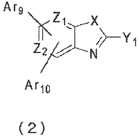
- [1] An organic EL device including at least an anode, a hole transport layer, a light-emitting layer, an electron transport layer, and a cathode in the stated order, the organic EL device being characterized in that the hole transport layer contains an arylamine compound represented by the following general formula (1), and the electron transport layer contains a compound having a benzoazole ring structure represented by the following general formula (2).

(In the formula, Ar1 to Ar5 may be the same or different from each other, and represent a substituted or unsubstituted aromatic hydrocarbon group, a substituted or unsubstituted aromatic heterocyclic group, or a substituted or unsubstituted fused polycyclic aromatic group. Ar6 to Ar8 may be the same or different from each other, and represent a hydrogen atom, a substituted or unsubstituted aromatic hydrocarbon group, a substituted or unsubstituted aromatic heterocyclic group, or a substituted or unsubstituted fused polycyclic aromatic group. n1 represents 0, 1, or 2. Ar3 and Ar4 may form a ring with a single bond or may be bonded to each other via a substituted or unsubstituted methylene group, an oxygen atom, or a sulfur atom to form a ring. Ar3 or Ar4 may form a ring with a benzene ring to which an Ar3Ar4-N group is bonded, with a single bond or may be bonded to each other via a substituted or unsubstituted methylene group, an oxygen atom, or a sulfur atom to form a ring.)
(In the formula, Ar9 and Ar10 may be the same or different from each other, and represent a hydrogen atom, a deuterium atom, a substituted or unsubstituted aromatic hydrocarbon group, a substituted or unsubstituted aromatic heterocyclic group, a substituted or unsubstituted fused polycyclic aromatic group, or a substituted or unsubstituted alkyl group. Y1 represents a substituted or unsubstituted aromatic hydrocarbon group, a substituted or unsubstituted aromatic heterocyclic group, a substituted or unsubstituted fused polycyclic aromatic group, or a substituted or unsubstituted alkyl group. X represents an oxygen atom or a sulfur atom. Z1 and Z2 may be the same or different from each other, and represent a carbon atom or a nitrogen atom.) - [2] The organic EL device according to [1] above, characterized in that the arylamine compound is represented by the following general formula (1a).
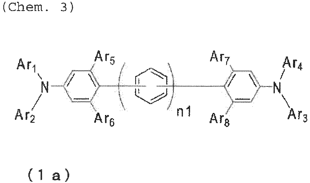
(In the formula, Ar1 to Ar5 may be the same or different from each other, and represent a substituted or unsubstituted aromatic hydrocarbon group, a substituted or unsubstituted aromatic heterocyclic group, or a substituted or unsubstituted fused polycyclic aromatic group. Ar6 to Ar8 may be the same or different from each other, and represent a hydrogen atom, a substituted or unsubstituted aromatic hydrocarbon group, a substituted or unsubstituted aromatic heterocyclic group, or a substituted or unsubstituted fused polycyclic aromatic group. n1 represents 0, 1, or 2. Ar3 and Ar4 may form a ring with a single bond, or may be bonded to each other via a substituted or unsubstituted methylene group, an oxygen atom, or a sulfur atom to form a ring. Ar3 or Ar4 may form a ring with a benzene ring to which an Ar3Ar4-N group is bonded, with a single bond or may be bonded to each other via a substituted or unsubstituted methylene group, an oxygen atom, or a sulfur atom to form a ring.) - [3] The organic EL device according to [1] or [2] above, characterized in that the compound having a benzoazole ring structure is represented by the following general formula (3).


(In the formula, Ar11 and Ar12 may be the same or different from each other, and represent a hydrogen atom, a deuterium atom, a substituted or unsubstituted aromatic hydrocarbon group, a substituted or unsubstituted aromatic heterocyclic group, a substituted or unsubstituted fused polycyclic aromatic group, or a substituted or unsubstituted alkyl group. Y2 represents a substituted or unsubstituted aromatic hydrocarbon group, a substituted or unsubstituted aromatic heterocyclic group, a substituted or unsubstituted fused polycyclic aromatic group, or a substituted or unsubstituted alkyl group. X represents an oxygen atom or a sulfur atom.) - [4] The organic EL device according to any one of [1] to [3] above, characterized in that the organic electroluminescence device further includes an electron blocking layer between the hole transport layer and the light-emitting layer.
- [5] The organic EL device according to [4] above, characterized in that the electron blocking layer contains an arylamine compound represented by the following general formula (4).
- (In the formula, Ar13 to Ar16 may be the same or different from each other, and represent a substituted or unsubstituted aromatic hydrocarbon group, a substituted or unsubstituted aromatic heterocyclic group, or a substituted or unsubstituted fused polycyclic aromatic group.)
- Specific examples of the "aromatic hydrocarbon group", "aromatic heterocyclic group", or "fused polycyclic aromatic group" in the "substituted or unsubstituted aromatic hydrocarbon group", "substituted or unsubstituted aromatic heterocyclic group", or "substituted or unsubstituted fused polycyclic aromatic group" represented by Ar1 to Ar8 in the general formulae (1) and (1a) include a phenyl group, a biphenylyl group, a terphenylyl group, a naphthyl group, an anthracenyl group, a phenanthrenyl group, a fluorenyl group, an indenyl group, a pyrenyl group, a perylenyl group, a fluoranthenyl group, a triphenylenyl group, a pyridyl group, a pyrimidinyl group, a triazinyl group, a furil group, a pyrrolyl group, a thienyl group, a quinolyl group, an isoquinolyl group, a benzofuranyl group, a benzothienyl group, an indolyl group, a carbazolyl group, a benzoxazolyl group, a benzothiazolyl group, a quinoxalinyl group, a benzimidazolyl group, a pyrazolyl group, a dibenzofuranyl group, a dibenzothienyl group, a naphthyridinyl group, a phenanthrolinyl group, an acridinyl group, and a carbolinyl group.
- Ar3 and Ar4 may form a ring with a single bond or may be bonded to each other via a substituted or unsubstituted methylene group, an oxygen atom, or a sulfur atom to form a ring, and Ar3 or Ar4 may form a ring with a benzene ring to which an Ar3Ar4-N group is bonded, with a single bond or may be bonded to each other via a substituted or unsubstituted methylene group, an oxygen atom, or a sulfur atom to form a ring.
- Specific examples of the "a substituted group" in the "substituted aromatic hydrocarbon group", "substituted aromatic heterocyclic group", or "substituted fused polycyclic aromatic group" represented by Ar1 to Ar8 in the general formulae (1) and (1a) include a deuterium atom, a cyano group, a nitro group; a halogen atom such as a fluorine atom, a chlorine atom, a bromine atom, and an iodine atom; a linear or branched alkyl group having 1 to 6 carbon atoms such as a methyl group, an ethyl group, an n-propyl group, an isopropyl group, an n-butyl group, an isobutyl group, a tert-butyl group, an n-pentyl group, an isopentyl group, a neopentyl group, and an n-hexyl group; a linear or branched alkyloxy group having 1 to 6 carbon atoms such as a methyloxy group, an ethyloxy group, and a propyloxy group; an alkenyl group such as a vinyl group, an allyl group; an aryloxy group such as a phenyloxy group and a tolyloxy group; an arylalkyloxy group such as a benzyloxy group and a phenethyloxy group; an aromatic hydrocarbon group or fused polycyclic aromatic group such as a phenyl group, a biphenylyl group, a terphenylyl group, a naphthyl group, an anthracenyl group, a phenanthrenyl group, a fluorenyl group, an indenyl group, a pyrenyl group, a perylenyl group, a fluoranthenyl group, and a triphenylenyl group; an aromatic heterocyclic group such as a pyridyl group, a pyrimidinyl group, a triazinyl group, a thienyl group, a furil group, a pyrrolyl group, a quinolyl group, an isoquinolyl group, a benzofuranyl group, a benzothienyl group, an indolyl group, a carbazolyl group, a benzoxazolyl group, a benzothiazolyl group, a quinoxalinyl group, a benzimidazolyl group, a pyrazolyl group, a dibenzofuranyl group, a dibenzothienyl group, and a carbolinyl group; an arylvinyl group such as a styryl group and a naphthylvinyl group; an acyl group such as an acetyl group and a benzoyl group, and these substituted groups may be further substituted with the exemplified substituted groups. Further, these substituted groups may form a ring with a single bond, or may be bonded to each other via a substituted or unsubstituted methylene group, an oxygen atom, or a sulfur atom to form a ring.
- The "aromatic hydrocarbon group", "aromatic heterocyclic group", or "fused polycyclic aromatic group" in the "substituted or unsubstituted aromatic hydrocarbon group", "substituted or unsubstituted aromatic heterocyclic group", or "substituted or unsubstituted fused polycyclic aromatic group" represented by Ar9 to Ar12, Y1, and Y2 in the general formulae (2) and (3) is selected from, specifically, the group consisting of an aryl group having 6 to 30 carbon atoms and a heteroaryl group having 2 to 20 carbo atoms in addition to a phenyl group, a biphenylyl group, a terphenylyl group, a naphthyl group, an anthracenyl group, a phenanthrenyl group, a fluorenyl group, a spirobifluorenyl group, an indenyl group, a pyrenyl group, a perylenyl group, a fluoranthenyl group, a triphenylenyl group, a pyridyl group, a pyrimidinyl group, a triazinyl group, a furil group, a pyrrolyl group, a thienyl group, a quinolyl group, an isoquinolyl group, a benzofuranyl group, a benzothienyl group, an indolyl group, a carbazolyl group, a benzoxazolyl group, a benzothiazolyl group, a quinoxalinyl group, a benzimidazolyl group, a pyrazolyl group, a dibenzofuranyl group, a dibenzothienyl group, a naphthyridinyl group, a phenanthrolinyl group, an acridinyl group, and a carbolinyl group.
- Specific examples of the "alkyl group" in the "substituted or unsubstituted alkyl group" represented by Ar9 to Ar12, Y1, and Y2 in the general formulae (2) and (3) include a methyl group, an ethyl group, an n-propyl group, an isopropyl group, an n-butyl group, an isobutyl group, a tert-butyl group, an n-pentyl group, an isopentyl group, a neopentyl group, an n-hexyl group, a cyclopentyl group, a cyclohexyl group, a 1-adamantyl group, a 2-adamantyl group, a vinyl group, an allyl group, an isopropenyl group, and a 2-buthenyl group.
- Examples of the "substituted group" in the "substituted aromatic hydrocarbon group", "substituted aromatic heterocyclic group", "substituted fused polycyclic aromatic group", or "substituted alkyl group" represented by Ar9 to Ar12, Y1, and Y2 in the general formulae (2) and (3) include the similar ones as described for the "substituted group" in the "substituted aromatic hydrocarbon group", "substituted aromatic heterocyclic group", or "substituted fused polycyclic aromatic group" represented by Ar1 to Ar8 in the general formulae (1) and (1a), and aspects similar to those of the "substituted group" in the "substituted aromatic hydrocarbon group", "substituted aromatic heterocyclic group", or "substituted fused polycyclic aromatic group" can be taken.
- Specific examples of the "aromatic hydrocarbon group", "aromatic heterocyclic group", or "fused polycyclic aromatic group" in the "substituted or unsubstituted aromatic hydrocarbon group", "substituted or unsubstituted aromatic heterocyclic group", or "substituted or unsubstituted fused polycyclic aromatic group" represented by Ar13 to Ar16 in the general formulae (4) include a phenyl group, a biphenylyl group, a terphenylyl group, a naphthyl group, an anthracenyl group, a phenanthrenyl group, a fluorenyl group, an indenyl group, a pyrenyl group, a perylenyl group, a fluoranthenyl group, a triphenylenyl group, a pyridyl group, a pyrimidinyl group, a triazinyl group, a furil group, a pyrrolyl group, a thienyl group, a quinolyl group, an isoquinolyl group, a benzofuranyl group, a benzothienyl group, an indolyl group, a carbazolyl group, a benzoxazolyl group, a benzothiazolyl group, a quinoxalinyl group, a benzimidazolyl group, a pyrazolyl group, a dibenzofuranyl group, a dibenzothienyl group, a naphthyridinyl group, a phenanthrolinyl group, an acridinyl group, and a carbolinyl group.
- Examples of the "substituted group" in the "substituted aromatic hydrocarbon group", "substituted aromatic heterocyclic group", or "substituted fused polycyclic aromatic group" represented by Ar13 to Ar16 in the general formula (4) include the similar ones as described for the "substituted group" in the "substituted aromatic hydrocarbon group", "substituted aromatic heterocyclic group", or "substituted fused polycyclic aromatic group" represented by Ar1 to Ar8 in the general formulae (1) and (1a), and aspects similar to those of the "substituted group" in the "substituted aromatic hydrocarbon group", "substituted aromatic heterocyclic group", or "substituted fused polycyclic aromatic group" can be taken.
- The arylamine compound that is represented by the general formula (1) and is suitably used for the organic EL device according to the present invention can be used as a constituent material of a hole injection layer or a hole transport layer of an organic EL device. The arylamine compound represented by the general formula (1) has a high mobility of holes, and is a favorable compound as a material for a hole injection layer or a hole transport layer.
- A compound that has a benzoazole ring structure, is represented by the general formula (2), and is suitably used for the organic EL device according to the present invention can be used as a constituent material of an electron transport layer of an organic EL device. This compound is favorable as a material of an electron transport layer because it has excellent electron injection/transport performance.
- Since in the organic EL device according to the present invention, an arylamine compound having a specific structure and a compound having a benzoazole ring structure with a specific structure as materials for an organic EL device excellent in hole/electron injection/transport performance, stability in a thin film sate, and durability are combined in consideration of carrier balance, the hole transport efficiency from the hole transport layer to the light-emitting layer and the electron transport efficiency from the electron transport layer to the light-emitting layer are improved (further, carrier balance is further refined in an aspect in which a material of a hole transport layer and a material of an electron blocking layer are combined so that holes can be injected/transported to the light-emitting layer more efficiently by using an arylamine compound having a specific structure as a material of the electron blocking layer) as compared with the existing organic EL device, thereby improving the light emission efficiency and reducing the driving voltage. Thus, it is possible to improve the durability of the organic EL device. The organic EL device according to the present invention is capable of realizing an organic EL device that has high efficiency, a low driving voltage, and particularly a long life time.
- The organic EL device according to the present invention is capable of efficiently injecting/transporting holes from the hole transport layer to the light-emitting layer and improving the efficiency of injecting/transporting electrons from the electron transport layer to the light-emitting layer by having selected a specific arylamine compound capable of effectively expressing the role of injecting/transporting holes and having selected a compound having a specific benzoazole ring structure capable of effectively expressing the role of injecting/transporting electrons, thereby making it possible to realizing an organic EL device that has excellent hole/electron injection/transport performance, stability in a thin film state, and durability and has high efficiency, a low driving voltage, and a long lifetime.
- In accordance with the present invention, it is possible to improve the light emission efficiency, driving voltage, and durability of the existing organic EL device.
-
- [
Fig. 1] Fig. 1 is a diagram showing the structural formulae of Compounds 1-1 to 1-15 as arylamine compounds represented by the general formula (1). - [
Fig. 2] Fig. 2 is a diagram showing the structural formulae of Compounds 1-16 to 1-30 as arylamine compounds represented by the general formula (1) . - [
Fig. 3] Fig. 3 is a diagram showing the structural formulae of Compounds 1-31 to 1-44 as arylamine compounds represented by the general formula (1) . - [
Fig. 4] Fig. 4 is a diagram showing the structural formulae of Compounds 2-1 to 2-10 as benzoxazole compounds represented by the general formula (2). - [
Fig. 5] Fig. 5 is a diagram showing the structural formulae of Compounds 2-11 to 2-20 as benzoxazole compounds represented by the general formula (2). - [
Fig. 6] Fig. 6 is a diagram showing the structural formulae of Compounds 2-21 to 2-30 as benzoxazole compounds represented by the general formula (2). - [
Fig. 7] Fig. 7 is a diagram showing the structural formulae of Compounds 2-31 to 2-42 as benzoxazole compounds represented by the general formula (2). - [
Fig. 8] Fig. 8 is a diagram showing the structural formulae of Compounds 2-43 to 2-54 as benzoxazole compounds represented by the general formula (2). - [
Fig. 9] Fig. 9 is a diagram showing the structural formulae of Compounds 2-55 to 2-68 as benzoxazole compounds represented by the general formula (2). - [
Fig. 10] Fig. 10 is a diagram showing the structural formulae of Compounds 2-69 to 2-80 as benzoxazole compounds represented by the general formula (2). - [
Fig. 11] Fig. 11 is a diagram showing the structural formulae of Compounds 2-81 to 2-92 as benzoxazole compounds represented by the general formula (2). - [
Fig. 12] Fig. 12 is a diagram showing the structural formulae of Compounds 2-93 to 2-102 as benzoxazole compounds represented by the general formula (2). - [
Fig. 13] Fig. 13 is a diagram showing the structural formulae of Compounds 2-103 to 2-113 as benzoxazole compounds represented by the general formula (2). - [
Fig. 14] Fig. 14 is a diagram showing the structural formulae of Compounds 2-114 to 2-125 as benzoxazole compounds represented by the general formula (2). - [
Fig. 15] Fig. 15 is a diagram showing the structural formulae of Compounds 2-126 to 2-133 as benzoxazole compounds represented by the general formula (2). - [
Fig. 16] Fig. 16 is a diagram showing the structural formulae of Compounds 3-1 to 3-10 as benzothiazole compounds represented by the general formula (3). - [
Fig. 17] Fig. 17 is a diagram showing the structural formulae of Compounds 3-11 to 3-20 as benzothiazole compounds represented by the general formula (3). - [
Fig. 18] Fig. 18 is a diagram showing the structural formulae of Compounds 3-21 to 3-30 as benzothiazole compounds represented by the general formula (3). - [
Fig. 19] Fig. 19 is a diagram showing the structural formulae of Compounds 3-31 to 3-42 as benzothiazole compounds represented by the general formula (3). - [
Fig. 20] Fig. 20 is a diagram showing the structural formulae of Compounds 3-43 to 3-53 as benzothiazole compounds represented by the general formula (3). - [
Fig. 21] Fig. 21 is a diagram showing the structural formulae of Compounds 3-54 to 3-63 as benzothiazole compounds represented by the general formula (3). - [
Fig. 22] Fig. 22 is a diagram showing the structural formulae of Compounds 4-1 to 4-15 as arylamine compounds represented by the general formula (4) . - [
Fig. 23] Fig. 23 is a diagram showing the structural formulae of Compounds 4-16 to 4-30 as arylamine compounds represented by the general formula (4) . - [
Fig. 24] Fig. 24 is a diagram showing the structural formulae of Compounds 4-31 to 4-45 as arylamine compounds represented by the general formula (4) . - [
Fig. 25] Fig. 25 is a diagram showing the structural formulae of Compounds 4-46 to 4-60 as arylamine compounds represented by the general formula (4) . - [
Fig. 26] Fig. 26 is a diagram showing the structural formulae of Compounds 4-61 to 4-75 as arylamine compounds represented by the general formula (4) . - [
Fig. 27] Fig. 27 is a diagram showing the structural formulae of Compounds 4-76 to 4-90 as arylamine compounds represented by the general formula (4) . - [
Fig. 28] Fig. 28 is a diagram showing the structural formulae of Compounds 4-91 to 4-105 as arylamine compounds represented by the general formula (4) . - [
Fig. 29] Fig. 29 is a diagram showing the structural formulae of Compounds 4-106 to 4-118 as arylamine compounds represented by the general formula (4) . - [
Fig. 30] Fig. 30 is a diagram showing the structural formulae of Compounds 4-119 to 4-133 as arylamine compounds represented by the general formula (4) . - [
Fig. 31] Fig. 31 is a diagram showing the structural formulae of Compounds 4-134 to 4-148 as arylamine compounds represented by the general formula (4) . - [
Fig. 32] Fig. 32 is a diagram showing the structural formulae of Compounds 4-149 to 4-163 as arylamine compounds represented by the general formula (4) . - [
Fig. 33] Fig. 33 is a diagram showing the structural formulae of Compounds 4-164 to 4-178 as arylamine compounds represented by the general formula (4) . - [
Fig. 34] Fig. 34 is a diagram showing the structural formulae of Compounds 4-179 to 4-193 as arylamine compounds represented by the general formula (4) . - [
Fig. 35] Fig. 35 is a diagram showing the structural formulae of Compounds 4-194 to 4-201 as arylamine compounds represented by the general formula (4) . - [
Fig. 36] Fig. 36 is a diagram showing a configuration of organic EL devices according to Examples 10 to 15 and Comparative Examples 1 to 7. Mode(s) for Carrying Out the Invention - Compounds 1-1 to 1-44 are shown in
Fig. 1 to Fig. 3 as specific examples of favorable compounds among the arylamine compounds represented by the general formula (1), which are favorably used for the organic EL element according to the present invention. However, the present invention is not limited to these compounds. - Compounds 2-1 to 2-133 are shown in
Fig. 4 to Fig. 15 as specific examples of favorable compounds among the benzoxazole compounds represented by the general formula (2), which are favorably used for the organic EL element according to the present invention. However, the present invention is not limited to these compounds. - Compounds 3-1 to 3-63 are shown in
Fig. 16 to Fig. 21 as specific examples of favorable compounds among the benzothiazole compounds represented by the general formula (2), which are favorably used for the organic EL element according to the present invention. However, the present invention is not limited to these compounds. - Compounds 4-1 to 4-201 are shown in
Fig. 22 to Fig. 35 as specific examples of favorable compounds among the arylamine compounds represented by the general formula (4), which are favorably used for the organic EL element according to the present invention. However, the present invention is not limited to these compounds. - Purification of compounds represented by the general formulae (1) to (4) was carried out by purification by column chromatography, adsorption purification with silica gel, activated carbon, activated clay, or the like, recrystallization with a solvent, a crystallization method, or the like, and finally purification by sublimation purification or the like was performed. Identification of the compounds was performed by NMR analysis. As physical property values, a glass transition point (Tg) and a work function were measured. The glass transition point (Tg) is an index of stability in a thin film state. The work function is an index of a hole transport property.
- The melting point and the glass transition point (Tg) were measured with a powder using a high sensitivity differential scanning calorimeter (DSC3100SA manufactured by Bruker AXS GmbH).
- The work function was obtained by preparing a thin film of 100 nm on an ITO substrate and using an ionization potential measuring apparatus (PYS-202 manufactured by Sumitomo Heavy Industries, Ltd.).
- Examples of the structure of the organic EL device according to the present invention include those including an anode, a hole injection layer, a hole transport layer, a light-emitting layer, an electron transport layer, an electron injection layer, and a cathode in the stated order on a substrate, those including an electron blocking layer between the hole transport layer and the light-emitting layer, and those including a hole blocking layer between the light-emitting layer and the electron transport layer. In the multilayer structures, several organic layers can be omitted or combined. For example, the hole injection layer and the hole transport layer may be combined or the electron injection layer and the electron transport layer may be combined. Further, two or more organic layers having the same function can be stacked. For example, two hole transport layers may be stacked, two light-emitting layers may be stacked, or two electron transport layers may be stacked.
- For the anode of the organic EL device according to the present invention, an electrode material having a large work function such as ITO and gold is used. As the hole injection layer of the organic EL device according to the present invention, a starburst type triphenylamine derivative, materials such as various triphenylamine tetramers; a porphyrin compound typified by copper phthalocyanine; an acceptor heterocyclic compound such as hexacyanoazatriphenylene, a coating type polymer material, or the like in addition to the arylamine compounds represented by the general formulae (1) and (1a) can be used. These materials can be formed into a thin film by a known method such as a spin coat method and an ink jet method in addition to a vapor deposition method.
- For the hole transport layer of the organic EL device according to the present invention, the arylamine compounds represented by the general formulae (1) and (1a) are used. These materials may be deposited alone. However, any of the materials may be mixed with another material and used as a single deposited layer. Further, a stacked structure of layers deposited alone, layers mixed and deposited, or at least one layer deposited alone and at least one layer mixed and deposited may be achieved. These materials can be formed into a thin film by a known method such as a spin coat method and an ink jet method in addition to a vapor deposition method.
- Further, in the hole injection layer or the hole transport layer, those obtained by P-doping a material typically used for the layer with trisbromophenylamine hexachloroantimony, a radialene derivative (see, for example, Patent Literature 6), or the like, a polymer compound having, as a partial structure, the structure of a benzidine derivative such as TPD, or the like can be used.
- For the hole transport layer of the organic EL device according to the present invention, a benzidine derivative such as N,N'-diphenyl-N,N'-di(m-tolyl)benzidine (TPD), N,N'-diphenyl-N,N'-di(α-naphthyl)benzidine (NPD), and N,N,N',N'-tetrabiphenylylbenzidine, an arylamine compound having two triphenylamine structures in the molecule, each of which is bonded via a single bond or a divalent group containing no hetero atom, such as 1,1-bis[4-(di-4-tolylamino)phenyl]cyclohexane (TAPC), an arylamine compound having four triphenylamine structures in the molecule, each of which is bonded via a single bond or a divalent group containing no hetero atom, various triphenylamine trimers, or the like, in addition to the arylamine compounds represented by the general formulae (1) and (1a), can be used. These materials may be deposited alone. However, any of the materials may be mixed with another material and used as a single deposited layer. Further, a stacked structure of layers deposited alone, layers mixed and deposited, or at least one layer deposited alone and at least one layer mixed and deposited may be achieved. Further, for the hole injection/transport layer, a coating polymer material such as poly(3,4-ethylenedioxythiophene) (PEDOT)/poly(styrene sulfonate) (PSS) can be used. These materials can be formed into a thin film by a known method such as a spin coat method and an ink jet method in addition to a vapor deposition method.
- For the electron blocking layer of the organic EL device according to the present invention, an arylamine compound having four triphenylamine structures in the molecule, each of which is bonded via a single bond or a divalent group containing no hetero atom, an arylamine compound having two triphenylamine structures in the molecule, each of which is bonded via a single bond or a divalent group containing no hetero atom, a compound having an electron blocking property, such as a carbazol derivative such as 4,4',4"-tri(N-carbazolyl) triphenylamine (TCTA), 9,9-bis[4-(carbazol-9-yl)phenyl]fluorene, 1,3-bis(carbazol-9-yl)benzene (mCP), and 2,2-bis(4-carbazol-9-ylphenyl)adamantane (Ad-Cz), and a compound having a triphenylsilyl group and a triarylamine structure typified by 9-[4-(carbazol-9-yl)phenyl]-9-[4-(triphenylsilyl)phenyl]-9H-fluorene, in addition to the arylamine compound represented by the general formula (4), can be used. These materials may be deposited alone. However, any of the materials may be mixed with another material and used as a single deposited layer. Further, a stacked structure of layers deposited alone, layers mixed and deposited, or at least one layer deposited alone and at least one layer mixed and deposited may be achieved. These materials can be formed into a thin film by a known method such as a spin coat method and an ink jet method in addition to a vapor deposition method.
- For the light-emitting layer of the organic EL device according to the present invention, various metal complexes, an anthracene derivative a bis-styryl benzene derivative, a pyrene derivative, an oxazole derivative, a polyparaphenylene vinylene derivative, or the like, in addition to a metal complex of a quinolinol derivative including Alq3, can be used. Further, the light-emitting layer may be formed of a host material and a dopant material. As the host material, an anthracene derivative is favorably used. In addition, not only the above-mentioned light-emitting material but also a heterocyclic compound having an indole ring as a partial structure of the fused ring, a heterocyclic compound having a carbazol ring as a partial structure of the fused ring, a carbazol derivative, a thiazole derivative, a benzimidazole derivative, a polydialkylfluorene derivative, or the like can be used. Further, as the dopant material, a pyrene derivative and an amine derivative having a fluorene ring as a partial structure of the fused ring are favorably used. In addition, quinacridone, coumarin, rubrene, perylene, and derivatives thereof, a benzopyran derivative, an indenophenanthrene derivative, a rhodamine derivative, an aminostyryl derivative, or the like can be used. These materials may be deposited alone. However, any of the materials may be mixed with another material and used as a single deposited layer. Further, a stacked structure of layers deposited alone, layers mixed and deposited, or at least one layer deposited alone and at least one layer mixed and deposited may be achieved.
- Further, as the light-emitting material, a phosphorescent material can be used. As the phosphorescent material, a phosphorescent material of a metal complex such as iridium and platinum can be used. A green phosphorescent material such as Ir(ppy)3, a blue phosphorescent material such as FIrpic and FIr6, a red phosphorescent material such as Btp2Ir (acac), or the like is used. As the host material (having a hole injection/transporting property) at this time, a carbazol derivative such as 4,4'-di(N-carbazolyl) biphenyl (CBP), TCTA, and mCP can be used. As a host material having an electron transportability, p-bis(triphenylsilyl)benzene (UGH2), 2,2',2"-(1,3,5-phenylene)-tris(1-phenyl-1H-benzimidazole) (TPBI), or the like can be used, and an organic EL device having high performance can be prepared.
- In order to avoid concentration quenching, it is favorable to dope the host material with the phosphorescent material by co-deposition in the range of 1 to 30 weight percent with respect to the entire light-emitting layer.
- Further, as the light-emitting material, a material emitting delayed fluorescence such as a CDCB derivative including PIC-TRZ, CC2TA, PXZ-TRZ, and 4CzIPN can be used (see, for example, Non-Patent Literature 3).
- These materials can be formed into a thin film by a known method such as a spin coat method and an ink jet method in addition to a vapor deposition method.
- For the hole blocking layer of the organic EL device according to the present invention, a compound having a hole blocking effect, such as various rare earth complexes, a triazole derivative, a triazine derivative, and an oxadiazole derivative, in addition to a phenanthroline derivative such as bathocuproin (BCP) and metal complex of a quinolinol derivative such as aluminum (III) bis (2-methyl-8-quinolinate) -4-phenylphenolate (BAlq), can be used. These materials may double as the material of the electron transport layer. These materials may be deposited alone. However, any of the materials may be mixed with another material and used as a single deposited layer. Further, a stacked structure of layers deposited alone, layers mixed and deposited, or at least one layer deposited alone and at least one layer mixed and deposited may be achieved. These materials can be formed into a thin film by a known method such as a spin coat method and an ink jet method in addition to a vapor deposition method.
- For the electron transport layer of the organic EL device according to the present invention, a compound having a benzoazole ring structure, which is represented by the general formula (2) or (3), is used. These materials may be deposited alone. However, any of the materials may be mixed with another material and used as a single deposited layer. Further, a stacked structure of layers deposited alone, layers mixed and deposited, or at least one layer deposited alone and at least one layer mixed and deposited may be achieved. These materials can be formed into a thin film by a known method such as a spin coat method and an ink jet method in addition to a vapor deposition method.
- For the electron transport layer of the organic EL device according to the present invention, a metal complex of a quinolinol derivative including Alq3 and BAlq, various metal complexes, a triazole derivative, a triazine derivative, an oxadiazole derivative, a pyridine derivative, a pyrimidine derivative, a benzimidazole derivative, a thiadiazole derivative, an anthracene derivative, a carbodiimide derivative, a quinoxaline derivative, a pyridoindole derivative, a phenanthroline derivative, a silole derivative, or the like, in addition to the compounds having a benzoazole ring structure, which are represented by the general formulae (2) and (3), can be used. These materials may be deposited alone. However, any of the materials may be mixed with another material and used as a single deposited layer. Further, a stacked structure of layers deposited alone, layers mixed and deposited, or at least one layer deposited alone and at least one layer mixed and deposited may be achieved. These materials can be formed into a thin film by a known method such as a spin coat method and an ink jet method in addition to a vapor deposition method.
- For the electron injection layer of the organic EL device according to the present invention, an alkali metal salt such as lithium fluoride and cesium fluoride, an alkaline earth metal salt such as magnesium fluoride, a metal oxide such as an aluminum oxide, a metal such as ytterbium (Yb), samarium (Sm), calcium (Ca), strontium (Sr), and cesium (Cs), or the like can be used. However, this can be omitted in the favorable selection of the electron transport layer and the cathode.
- In the cathode of the organic EL device according to the present invention, an electrode material having a low work function, such as aluminum, an alloy having a lower work function, such as a magnesium silver alloy, a magnesium indium alloy, and an aluminum magnesium alloy, or the like is used as the electrode material.
- Hereinafter, the embodiment of the present invention will be specifically described by way of Examples. However, the present invention is not limited to the following Examples.
- (9,9-dimethylfluoren-2-yl)-(biphenyl-4-yl)-(6-brombiphenyl-3-yl)amine: 10.0 g, 4-{(biphenyl-4-yl)-phenylamino} phenylboronic acid: 7.9 g, tetrakistriphenylphosphine palladium (0): 0.60 g, potassium carbonate: 5.0 g, toluene: 80 ml, ethanol: 40 ml, and water: 30 ml were added to a reaction vessel purged with nitrogen, and the mixture was heated and stirred at 100°C overnight. After the mixture was cooled, an organic layer was extracted by liquid separation and then the extract was concentrated and purified by column chromatography (carrier: silica gel, eluent: dichloromethane/heptane). Thus, a white powder of 4-{(9,9-dimethylfluoren-2-yl)-(biphenyl-4-yl)amino}-4'-(biphenyl-4-yl-phenylamino)-2-phenyl-biphenyl (Compound 1-7): 8.30 g (yield of 49%) was obtained.
- The structure of the obtained white powder was identified using NMR.
- The following 48 hydrogen signals were detected by 1H-NMR (CDCl3).
- δ(ppm)=7.72-7.60(2H), 7.59-7.52(2H), 7.51-7.10(35), 7.09-6.90(3H), 1.56(6H).

- By using 4-(diphenylamino) phenylboronic acid instead of 4-{(biphenyl-4-yl)-phenylamino} phenylboronic acid in Example 1 and performing the reaction under similar conditions, a white powder of 4-{(9,9-dimethylfluoren-2-yl)-(biphenyl-4-yl)amino}-4'-(diphenylamino)-2-phenyl-biphenyl (Compound 1-11): 11.5 g (yield of 75%) was obtained.
- The structure of the obtained white powder was identified using NMR.
- The following 44 hydrogen signals were detected by 1H-NMR (CDCl3).
- δ(ppm)=7.71-7.64(4H), 7.58-7.56(2H), 7.49-6.94(32), 1.51(6H).

- By using (9,9-dimethylfluoren-2-yl)-phenyl-(6-brombiphenyl-3-yl) amine instead of (9,9-dimethylfluoren-2-yl)-(biphenyl-4-yl)-(6-brombiphenyl-3-yl) amine in Example 1 and performing the reaction under similar conditions, a white powder of 4-{(9,9-dimethylfluoren-2-yl)-phenylamino}-4'-(biphenyl-4-yl-phenylamino)-2-phenyl-biphenyl (Compound 1-14): 10.2 g (yield of 69%) was obtained.
- The structure of the obtained white powder was identified using NMR.
- The following 44 hydrogen signals were detected by 1H-NMR (CDCl3).
- δ(ppm)=7.69-7.59(4H), 7.48-7.42(4H), 7.37-6.98(30), 1.49(6H).

- The melting point and the glass transition point of the arylamine compound represented by the general formula (1) were measured using a high sensitivity differential scanning calorimeter (DSC3100S manufactured by Bruker AXS GmbH).
- Melting point Glass transition point
Compound of Example 1 Not observed 125°C Compound of Example 2 Not observed 117°C Compound of Example 3 Not observed 114°C - The arylamine compound represented by the general formula (1) has the glass transition point of 100°C or more, which indicates that it is stable in a thin film state.
- The arylamine compound represented by the general formula (1) was used to prepare a vapor deposition film having a film thickness of 100 nm on an ITO substrate, and the work function thereof was measured by an ionization potential measuring apparatus (PYS-202 manufactured by Sumitomo Heavy Industries, Ltd.).
Work Function Compound of Example 1 5.57 eV Compound of Example 2 5.62 eV Compound of Example 3 5.59 eV - It can be seen that the arylamine compound represented by the general formula (1) has favorable hole transport performance because it has a more favorable energy level than the work function that a general hole transport material such as NPD and TPD has, which is 5.4 eV.
- 2- (4-chloro-phenyl) -4,6-bis (naphthalen-1-yl-phenyl) -benzoxazole: 4.5 g, 3-pyridylboronic acid: 1.0 g, bis(dibenzylideneacetone) palladium (0): 0.32g, tricyclohexylphosphine: 0.4g, and tripotassium phosphate were charged into a reaction vessel and stirred under reflux overnight. The mixture was allowed to cool and then separated. Extraction was performed with ethyl acetate from the aqueous layer, and then, the extract was concentrated. The crude product thus obtained was purified by column chromatography (carrier: silica gel, eluent: dichloromethane/ethyl acetate), and then crystallized with dichloromethane/methanol. Thus, a white powder of 4,6-bis(naphthalen-1-yl-phenyl)-2-14-(pyridin-3-yl)-phenyl}-benzoxazole (Compound 2-1): 1.8 g (yield of 38%) was obtained.

- The structure of the obtained white powder was identified using NMR.
- The following 32 hydrogen signals were detected by 1H-NMR (CDCl3).
- δ(ppm)=8.98(1H), 8.68(1H), 8.52(2H), 8.34(2H), 8.12(1H), 8.07-7.89(10H), 7.82(2H), 7.76(2H), 7.69(2H), 7.64(9H).
- By using 2-(4-chloro-phenyl)-6-(phenanthren-9-yl)-4-{4-(pyridin-3-yl)-phenyl}-benzoxazole, 3-pyridylboronic acid, and bis(dibenzylideneacetone) palladium (0) instead of 2-(4-chlorophenyl)-4,6-bis(naphthalen-1-ylphenyl)-benzoxazole, phenylboronic acid, and tris (dibenzylideneacetone) palladium (0) in Example 6, respectively, and performing the reaction under similar conditions, a white powder of 2-(biphenyl-4-yl)-6-(phenanthren-9-yl)-4-{4-(pyridin-3-yl)-phenyl}-benzoxazole (Compound 1-118): 4.3 g (yield of 67%) was obtained.

- The structure of the obtained white powder was identified using NMR.
- The following 28 hydrogen signals were detected by 1H-NMR (CDCl3).
- δ(ppm)=8.98(1H), 8.86(1H), 8.80(1H), 8.64(1H), 8.46(2H), 8.32(2H), 8.07(1H), 7.98(2H), 7.88-7.57(13H), 7.52 (2H), 7.44 (2H) .
- The melting point and the glass transition point of the benzoazole compound represented by the general formula (2) were measured using a high sensitivity differential scanning calorimeter (DSC3100SA manufactured by Bruker AXS GmbH).
- Melting point Glass transition point
Compound of Example 6 Not observed 128°C Compound of Example 7 Not observed 132°C - The benzoazole compound represented by the general formula (2) has the glass transition point of 100°C or more, which indicates that it is stable in a thin film state.
- The benzoazole compound represented by the general formula (2) was used to prepare a vapor deposition film having a film thickness of 100 nm on an ITO substrate, and the work function thereof was measured by an ionization potential measuring apparatus (PYS-202 manufactured by Sumitomo Heavy Industries, Ltd.).
Work Function Compound of Example 6 6.34 eV Compound of Example 7 6.43 eV - The compound having a benzoazole ring structure represented by the general formula (2) has a value of work function larger than 5.4 eV that is a value of work function of a general hole transport material such as NPD and TPD and has large hole blocking performance.
- The organic EL device was prepared by depositing a
hole injection layer 3, ahole transport layer 4, anelectron blocking layer 5, a light-emittinglayer 6, anelectron transport layer 7, anelectron injection layer 8, and a cathode (aluminum electrode) 9 in the stated order on atransparent anode 2, which has been formed on aglass substrate 1 as an ITO electrode in advance, as shown inFig. 36 . - Specifically, after performing, in isopropyl alcohol for 20 minutes, ultrasonic cleaning on the
glass substrate 1 on which ITO having a film thickness of 50 nm was formed, theglass substrate 1 was dried for 10 minutes on a hot plate heated to 200°C. After that, UV ozone treatment was performed for 15 minutes, and then, the ITO-attached glass substrate was mounted in a vacuum deposition machine. The pressure in the vacuum deposition machine was reduced to 0.001 Pa or less. Subsequently, a film of an electron acceptor (Acceptor-1) having the following structural formula and the Compound (1-7) according to Example 1 was formed, as thehole injection layer 3, to have a film thickness of 10 nm and cover thetransparent anode 2 by binary deposition at a deposition rate in which the ratio of the deposition rates of (Acceptor-1) and the Compound (1-7) was 3:97. As thehole transport layer 4, a film of the Compound (1-7) according to the Example 1 was formed on thehole injection layer 3 to have a film thickness of 50 nm. A film of the Compound (4-158) having the following structural formula was formed, as theelectron blocking layer 5, on thehole transport layer 4 to have a film thickness of 5 nm. A film of a Compound (EMD-1) having the following structural formula and a Compound (EMH-1) having the following structural formula was formed, as the light-emittinglayer 6, on theelectron blocking layer 5 to have a film thickness of 20 nm by binary deposition at a deposition rate in which the ratio of the deposition rates of (EMD-1) and (EMH-1) was 5:95. A film of the Compound (2-1) according to Example 6 and a Compound (ETM-1) having the following structural formula was formed on the light-emittinglayer 6, as theelectron transport layer 7 to have a film thickness of 30 nm by binary deposition at a deposition rate in which the ratio of the deposition rates of Compound (2-1) and the Compound (ETM-1) was 50:50. A film of lithium fluoride was formed, as theelectron injection layer 8, on theelectron transport layer 7 to have a film thickness of 1 nm. Finally, aluminum was deposited to have a thickness of 100 nm to form thecathode 9. The characteristics of the prepared organic EL device were measured at room temperature in the atmosphere. The measurement results of the light-emitting characteristics when a direct current voltage was applied to the prepared organic EL device were collectively shown in Table 1.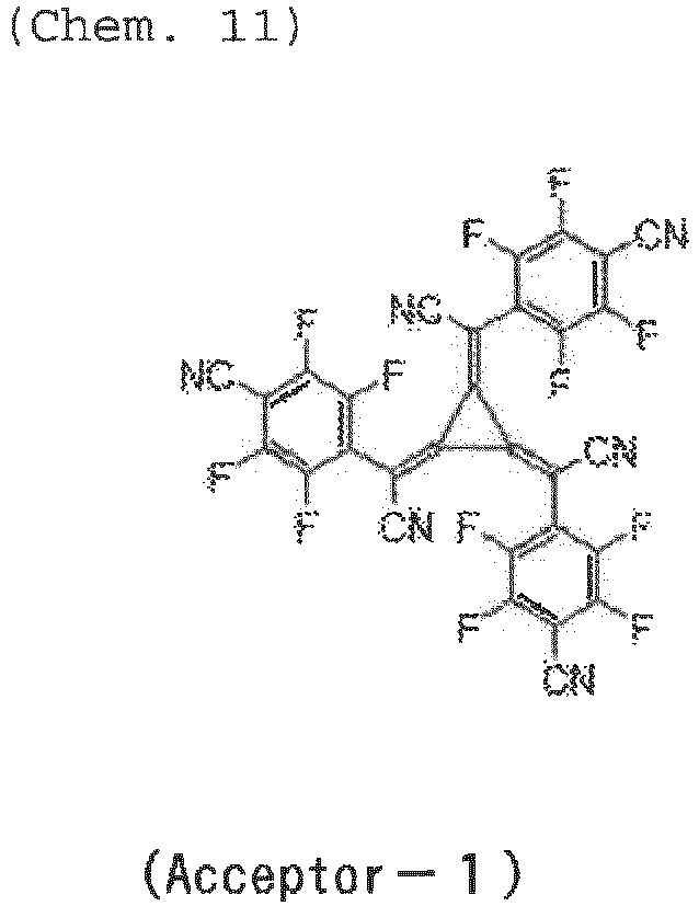


- An organic EL device was prepared in similar conditions to Example 10 except that the Compound (1-11) according to Example 2 was used for the material of the
hole injection layer 3 and thehole transport layer 4 instead of the Compound (1-7) according to Example 1. The characteristics of the prepared organic EL device were measured at room temperature in the atmosphere. The measurement results of the light-emitting characteristics when a direct current voltage was applied to the prepared organic EL device were collectively shown in Table 1.
- An organic EL device was prepared in similar conditions to Example 10 except that the Compound (1-14) according to Example 3 was used for the material of the
hole injection layer 3 and thehole transport layer 4 instead of the Compound (1-7) according to Example 1. The characteristics of the prepared organic EL device were measured at room temperature in the atmosphere. The measurement results of the light-emitting characteristics when a direct current voltage was applied to the prepared organic EL device were collectively shown in Table 1.

- An organic EL device was prepared in similar conditions to Example 10 except that the Compound (2-118) according to Example 7 was used for the material of the
electron transport layer 7 instead of the Compound (2-1) according to Example 6. The characteristics of the prepared organic EL device were measured at room temperature in the atmosphere. The measurement results of the light-emitting characteristics when a direct current voltage was applied to the prepared organic EL device were collectively shown in Table 1.

- An organic EL device was prepared in similar conditions to Example 10 except that the Compound (1-11) according to Example 2 was used for the material of the
hole injection layer 3 and thehole transport layer 4 instead of the Compound (1-7) according to Example 1 and the Compound (2-118) according to Example 7 was used for the material of theelectron transport layer 7 instead of the Compound (2-1) according to Example 6. The characteristics of the prepared organic EL device were measured at room temperature in the atmosphere. The measurement results of the light-emitting characteristics when a direct current voltage was applied to the prepared organic EL device were collectively shown in Table 1. - An organic EL device was prepared in similar conditions to Example 10 except that the Compound (1-14) according to Example 3 was used for the material of the
hole injection layer 3 and thehole transport layer 4 instead of the Compound (1-7) according to Example 1 and the Compound (2-118) according to Example 7 was used for the material of theelectron transport layer 7 instead of the Compound (2-1) according to Example 6. The characteristics of the prepared organic EL device were measured at room temperature in the atmosphere. The measurement results of the light-emitting characteristics when a direct current voltage was applied to the prepared organic EL device were collectively shown in Table 1. - For comparison, an organic EL device was prepared in similar conditions to Example 10 except that the Compound (HTM-1) having the following structure was used for the material of the
hole injection layer 3 and thehole transport layer 4 instead of the Compound (1-7) according to Example 1. The characteristics of the prepared organic EL device were measured at room temperature in the atmosphere. The measurement results of the light-emitting characteristics when a direct current voltage was applied to the prepared organic EL device were collectively shown in Table 1.

- For comparison, an organic EL device was prepared in similar conditions to Example 10 except that the Compound (HTM-1) having the following structure was used for the material of the
hole injection layer 3 and thehole transport layer 4 instead of the Compound (1-7) according to Example 1 and the Compound (2-118) according to Example 7 was used for the material of theelectron transport layer 7 instead of the Compound (2-1) according to Example 6. The characteristics of the prepared organic EL device were measured at room temperature in the atmosphere. The measurement results of the light-emitting characteristics when a direct current voltage was applied to the prepared organic EL device were collectively shown in Table 1. - For comparison, an organic EL device was prepared in similar conditions to Example 10 except that the Compound (HTM-2) having the following structural formula was used for the material of the
hole injection layer 3 and thehole transport layer 4 instead of the Compound (1-7) according to Example 1. The characteristics of the prepared organic EL device were measured at room temperature in the atmosphere. The measurement results of the light-emitting characteristics when a direct current voltage was applied to the prepared organic EL device were collectively shown in Table 1.
- For comparison, an organic EL device was prepared in similar conditions to Example 10 except that the Compound (HTM-2) having the following structural formula was used for the material of the
hole injection layer 3 and thehole transport layer 4 instead of the Compound (1-7) according to Example 1 and the Compound (2-118) according to Example 7 was used for the material of theelectron transport layer 7 instead of the Compound (2-1) according to Example 6. The characteristics of the prepared organic EL device were measured at room temperature in the atmosphere. The measurement results of the light-emitting characteristics when a direct current voltage was applied to the prepared organic EL device were collectively shown in Table 1. - For comparison, an organic EL device was prepared in similar conditions to Example 10 except that the Compound (HTM-2) having the following structural formula was used for the material of the
electron transport layer 7 instead of the Compound (2-1) according to Example 6. The characteristics of the prepared organic EL device were measured at room temperature in the atmosphere. The measurement results of the light-emitting characteristics when a direct current voltage was applied to the prepared organic EL device were collectively shown in Table 1.

- For comparison, an organic EL device was prepared in similar conditions to Example 10 except that the Compound (1-11) according to Example 2 was used for the material of the
hole transport layer 4 instead of the Compound (1-7) according to Example 1 and the Compound (HTM-2) having the following structural formula was used for the material of theelectron transport layer 7 instead of the Compound (2-1) according to Example 6. The characteristics of the prepared organic EL device were measured at room temperature in the atmosphere. The measurement results of the light-emitting characteristics when a direct current voltage was applied to the prepared organic EL device were collectively shown in Table 1. - For comparison, an organic EL device was prepared in similar conditions to Example 10 except that the Compound (1-14) according to Example 3 was used for the material of the
hole transport layer 4 instead of the Compound (1-7) according to Example 1 and the Compound (HTM-2) having the following structural formula was used for the material of theelectron transport layer 7 instead of the Compound (2-1) according to Example 6. The characteristics of the prepared organic EL device were measured at room temperature in the atmosphere. The measurement results of the light-emitting characteristics when a direct current voltage was applied to the prepared organic EL device were collectively shown in Table 1. - The device lifetime was measured using each of the organic EL devices prepared in Examples 10 to 15 and Comparative Examples 1 to 7, and the results were collectively shown in Table 1. The device lifetime was measured as the time until the light emission luminance attenuated to 1900 cd/m2 (corresponding to 95% in the case where the initial luminance was 100%: 95% attenuation) when constant current driving was performed with the light emission luminance (initial luminance) at the start of light emission set to 2000 cd/m2.
[Table 1] Hole transport layer Electron blocking layer Light-emitting layer Electron transport layer Voltage[V] (@ 10mA/cm2) Luminance[cd/m2] (@10mA/cm2) Light emission efficiency[cd/A] (@10mA/cm2) Power efficiency[lm/W] (@10mA/cm2) Element lifetime 95% attenuated Example 10 Compound 1-7 Compound 4-158 EMD-1/ EMH-1 Compound 2-1/ ETM-1 3.59 953 9.53 8.34 211 hours Example 11 Compound 1-11 Compound 4-158 EMD-1/ EMH-1 Compound 2-1/ ETM-1 3.57 1034 10.34 9.09 230 hours Example 12 Compound 1-14 Compound 4-158 EMD-1/ EMH-1 Compound 2-1/ ETM-1 3.56 986 9.86 8.71 213 hours Example 13 Compound 1-7 Compound 4-158 EMD-1/ EMH-1 Compound 2-118/ ETM-1 3.57 941 9.41 8.27 262 hours Example 14 Compound 1-11 Compound 4-158 EMD-1/ EMH-1 Compound 2-118/ ETM-1 3.54 1042 10.42 9.25 301 hours Example 15 Compound 1-14 Compound 4-158 EMD-1/ EMH-1 Compound 2-118/ ETM-1 3.55 998 9.98 8.85 286 hours Comparative Example 1 HTM-1 Compound 4-158 EMD-1/ EMH-1 Compound 2-1/ ETM-1 3.69 893 8.93 7.61 141 hours Comparative Example 2 HTM - 1 Compound 4-158 EMD-1/ EMH-1 Compound 2-118/ ETM-1 3.64 894 8.94 7.72 176 hours Comparative Example 3 HTM-2 Compound 4-158 EMD-1/ HMH-1 Compound 2-1/ ETM-1 3.71 875 8.75 7.42 122 hours Comparative Example 4 HTM-2 Compound 4-158 EMD-1/ EMH-1 Compound 2-118/ ETM-1 3.64 857 8.57 7.40 157 hours Comparative Example 5 Compound 1-7 Compound 4-158 EMD-1/ EMH-1 ETM-2/ ETM-1 4.01 659 6.59 5.16 137 hours Comparative Example 6 Compound 1-11 Compound 4-158 EMD-1/ EMH-1 ETM-2/ ETM-1 4.10 770 7.70 5.90 165 hours Comparative Example 7 Compound 1-14 Compound 4-158 EMD-1/ EMH-1 ETM-2/ ETM-1 4.00 736 7.36 5.79 152 hours - As shown in TAble 1, the light emission efficiency when a current having a current density of 10 mA/cm2 was caused to flow was high in any of the organic EL devices according to Examples 10 to 15, i.e., 9.41 to 10.42 cd/A, as compared with those of the organic EL devices according to Comparative Examples 1 to 7, i.e., 6.59 to 8.94 cd/A. Further, also the power efficiency was high in any of the organic EL devices according to Examples 10 to 15, i.e., 8.27 to 9.25 lm/W, as compared with those of the organic EL devices according to Comparative Examples 1 to 7, i.e., 5.16 to 7.72lm/W. Meanwhile, it can be seen that the device lifetime (95% attenuation) was largely extended to 211 to 301 hours in the organic EL devices according to Examples 10 to 15 as compared with 122 to 176 hours of the organic EL devices according to Comparative Examples 1 to 7.
- It has been found that the organic EL device according to the present invention is capable of realizing an organic EL device that has higher light emission efficiency and a longer lifetime than the existing organic EL device because the carrier balance inside the organic EL device is improved by combining a specific arylamine compound and a specific compound having a benzoazole ring structure and the combination is made so that the carrier balance matches the characteristics of the light-emitting material.
- The organic EL device according to the present invention, which is obtained by combining a specific arylamine compound and a specific compound having a benzoazole ring structure is capable of improving the light emission efficiency and the durability of the organic EL device. For example, it has become possible to expand to home appliances and lighting applications.
-
- 1
- glass substrate
- 2
- transparent anode
- 3
- hole injection layer
- 4
- hole transport layer
- 5
- electron blocking layer
- 6
- light-emitting layer
- 7
- electron transport layer
- 8
- electron injection layer
- 9
- cathode

Claims (5)
- An organic electroluminescence device including at least an anode, a hole transport layer, a light-emitting layer, an electron transport layer, and a cathode in the stated order, the organic electroluminescence device being characterized in that
the hole transport layer contains an arylamine compound represented by the following general formula (1), and
the electron transport layer contains a compound having a benzoazole ring structure represented by the following general formula (2).
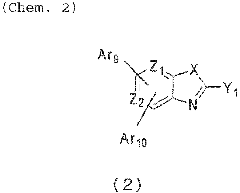
- The organic electroluminescence device according to claim 1, characterized in that
the arylamine compound is represented by the following general formula (1a).
- The organic electroluminescence device according to claim 1 or 2, characterized in that
the compound having a benzoazole ring structure is represented by the following general formula (3).
- The organic electroluminescence device according to any one of claims 1 to 3, characterized in that
the organic electroluminescence device further includes an electron blocking layer between the hole transport layer and the light-emitting layer. - The organic electroluminescence device according to claim 4, characterized in that
the electron blocking layer contains an arylamine compound represented by the following general formula (4) .
Applications Claiming Priority (2)
| Application Number | Priority Date | Filing Date | Title |
|---|---|---|---|
| JP2017175835 | 2017-09-13 | ||
| PCT/JP2018/032746 WO2019054233A1 (en) | 2017-09-13 | 2018-09-04 | Organic electroluminescent element |
Publications (3)
| Publication Number | Publication Date |
|---|---|
| EP3683852A1 true EP3683852A1 (en) | 2020-07-22 |
| EP3683852A4 EP3683852A4 (en) | 2021-06-23 |
| EP3683852B1 EP3683852B1 (en) | 2023-11-22 |
Family
ID=65722626
Family Applications (1)
| Application Number | Title | Priority Date | Filing Date |
|---|---|---|---|
| EP18855786.2A Active EP3683852B1 (en) | 2017-09-13 | 2018-09-04 | Organic electroluminescent element |
Country Status (7)
| Country | Link |
|---|---|
| US (1) | US11578065B2 (en) |
| EP (1) | EP3683852B1 (en) |
| JP (1) | JP7227141B2 (en) |
| KR (1) | KR102724791B1 (en) |
| CN (1) | CN111095588B (en) |
| TW (1) | TWI790280B (en) |
| WO (1) | WO2019054233A1 (en) |
Cited By (3)
| Publication number | Priority date | Publication date | Assignee | Title |
|---|---|---|---|---|
| EP3598516A4 (en) * | 2017-03-15 | 2021-01-13 | Hodogaya Chemical Co., Ltd. | ORGANIC ELECTROLUMINESCENT ELEMENT |
| CN113896740A (en) * | 2021-10-27 | 2022-01-07 | 武汉华星光电半导体显示技术有限公司 | Organic compound, preparation method thereof and light-emitting device |
| EP3890043A4 (en) * | 2018-11-29 | 2022-08-24 | Hodogaya Chemical Co., Ltd. | COMPOUND WITH AZABENZOXAZOLE RING STRUCTURE AND ORGANIC ELECTROLUMINESCENT ELEMENT |
Families Citing this family (1)
| Publication number | Priority date | Publication date | Assignee | Title |
|---|---|---|---|---|
| CN110105350A (en) * | 2019-05-21 | 2019-08-09 | 武汉华星光电半导体显示技术有限公司 | Luminous organic material and preparation method thereof, organic luminescent device |
Family Cites Families (25)
| Publication number | Priority date | Publication date | Assignee | Title |
|---|---|---|---|---|
| JPS4943840B1 (en) | 1970-12-25 | 1974-11-25 | ||
| JP3194657B2 (en) | 1993-11-01 | 2001-07-30 | 松下電器産業株式会社 | EL device |
| JP3828595B2 (en) | 1994-02-08 | 2006-10-04 | Tdk株式会社 | Organic EL device |
| TWI228017B (en) * | 2003-12-31 | 2005-02-11 | Ritdisplay Corp | Organic electroluminescent device |
| KR100787425B1 (en) | 2004-11-29 | 2007-12-26 | 삼성에스디아이 주식회사 | Phenylcarbazole compound and organic electroluminescent device using same |
| CN1956945B (en) | 2004-05-25 | 2010-09-22 | 保土谷化学工业株式会社 | P-terphenyl compound and electrophotographic photoreceptor using the same |
| JP5162847B2 (en) | 2006-05-31 | 2013-03-13 | セイコーエプソン株式会社 | Printer and printer control method |
| CN101535256B (en) | 2006-11-24 | 2013-05-22 | 出光兴产株式会社 | Aromatic amine derivative and organic electroluminescent element using same |
| KR101076156B1 (en) * | 2009-07-20 | 2011-10-21 | 기아자동차주식회사 | Method For Emission Controlling Of Diesel Particulate Filter |
| KR101282178B1 (en) * | 2010-01-18 | 2013-07-04 | 덕산하이메탈(주) | Aromatic amine compund having various permutator and organic electroric element using the same, terminal thererof |
| TW201132631A (en) | 2010-02-05 | 2011-10-01 | Nitto Denko Corp | Tris (arylbenzoxazole) benzene and tris (arylbenzothiazole) benzene and derivatives thereof as organic electron-transport materials |
| KR20120070468A (en) * | 2010-12-21 | 2012-06-29 | (주)씨에스엘쏠라 | Organic light compound and organic light device using the same |
| US9051274B2 (en) * | 2011-06-24 | 2015-06-09 | Semiconductor Energy Laboratory Co., Ltd. | Triarylamine compound, light-emitting element, light-emitting device, electronic device, and lighting device |
| EP2752904B1 (en) | 2012-05-31 | 2020-07-01 | LG Display Co., Ltd. | Organic light emitting diode |
| EP2684932B8 (en) | 2012-07-09 | 2016-12-21 | Hodogaya Chemical Co., Ltd. | Diarylamino matrix material doped with a mesomeric radialene compound |
| JP3194657U (en) | 2014-09-19 | 2014-12-04 | 恵美子 青柳 | Thermal necklace |
| KR102533039B1 (en) | 2015-01-06 | 2023-05-15 | 호도가야 가가쿠 고교 가부시키가이샤 | organic electroluminescence device |
| CN107534093B (en) * | 2015-04-27 | 2020-06-30 | 保土谷化学工业株式会社 | Organic electroluminescent device |
| WO2016197353A1 (en) * | 2015-06-11 | 2016-12-15 | Dow Global Technologies Llc | Organic electroluminescent compound and organic electroluminescent device comprising the same |
| JP6810710B2 (en) | 2016-01-14 | 2021-01-06 | 保土谷化学工業株式会社 | Organic electroluminescence device |
| KR102719558B1 (en) | 2016-02-12 | 2024-10-18 | 호도가야 가가쿠 고교 가부시키가이샤 | Organic electroluminescent devices |
| CN118772139A (en) * | 2016-03-15 | 2024-10-15 | 陶氏环球技术有限责任公司 | Organic electroluminescent compound and organic electroluminescent device thereof |
| KR102440762B1 (en) * | 2016-07-07 | 2022-09-05 | 호도가야 가가쿠 고교 가부시키가이샤 | A compound having a benzoazole ring structure and an organic electroluminescent device |
| CN110431680B (en) * | 2017-03-15 | 2022-07-08 | 保土谷化学工业株式会社 | Organic electroluminescent element |
| CN111344879B (en) * | 2017-11-16 | 2023-04-18 | 保土谷化学工业株式会社 | organic electroluminescent element |
-
2018
- 2018-09-04 EP EP18855786.2A patent/EP3683852B1/en active Active
- 2018-09-04 JP JP2019542008A patent/JP7227141B2/en active Active
- 2018-09-04 US US16/646,980 patent/US11578065B2/en active Active
- 2018-09-04 WO PCT/JP2018/032746 patent/WO2019054233A1/en not_active Ceased
- 2018-09-04 KR KR1020207009823A patent/KR102724791B1/en active Active
- 2018-09-04 CN CN201880059339.5A patent/CN111095588B/en active Active
- 2018-09-12 TW TW107132046A patent/TWI790280B/en active
Cited By (4)
| Publication number | Priority date | Publication date | Assignee | Title |
|---|---|---|---|---|
| EP3598516A4 (en) * | 2017-03-15 | 2021-01-13 | Hodogaya Chemical Co., Ltd. | ORGANIC ELECTROLUMINESCENT ELEMENT |
| EP3890043A4 (en) * | 2018-11-29 | 2022-08-24 | Hodogaya Chemical Co., Ltd. | COMPOUND WITH AZABENZOXAZOLE RING STRUCTURE AND ORGANIC ELECTROLUMINESCENT ELEMENT |
| US12024527B2 (en) | 2018-11-29 | 2024-07-02 | Hodogaya Chemical Co., Ltd. | Compound having azabenzoxazole ring structure and organic electroluminescent element |
| CN113896740A (en) * | 2021-10-27 | 2022-01-07 | 武汉华星光电半导体显示技术有限公司 | Organic compound, preparation method thereof and light-emitting device |
Also Published As
| Publication number | Publication date |
|---|---|
| CN111095588A (en) | 2020-05-01 |
| US11578065B2 (en) | 2023-02-14 |
| JP7227141B2 (en) | 2023-02-21 |
| KR102724791B1 (en) | 2024-10-31 |
| US20200207748A1 (en) | 2020-07-02 |
| EP3683852B1 (en) | 2023-11-22 |
| JPWO2019054233A1 (en) | 2020-08-27 |
| KR20200051720A (en) | 2020-05-13 |
| TWI790280B (en) | 2023-01-21 |
| EP3683852A4 (en) | 2021-06-23 |
| CN111095588B (en) | 2023-11-17 |
| TW201920602A (en) | 2019-06-01 |
| WO2019054233A1 (en) | 2019-03-21 |
Similar Documents
| Publication | Publication Date | Title |
|---|---|---|
| EP3156402B1 (en) | Pyrimidine derivative and organic electroluminescent element | |
| EP3690970B1 (en) | Organic electroluminescence device | |
| EP3754739A1 (en) | Organic electroluminescence element | |
| EP3483148A1 (en) | Compound having benzazole ring structure and organic electroluminescent element | |
| EP3664173B1 (en) | Organic electroluminescence element containing compound having benzoazole ring structure | |
| EP3683852B1 (en) | Organic electroluminescent element | |
| EP3514845B1 (en) | Indenocarbazole compound and organic electroluminescent element | |
| KR102813014B1 (en) | Compounds having an azabenzoxazole ring structure and organic electroluminescent devices | |
| EP3770158A1 (en) | Compound including benzimidazole ring structure and organic electroluminescent element | |
| EP3683212B1 (en) | Compound having pyrimidine ring structure and organic electroluminescent element | |
| KR102931947B1 (en) | Compounds having a benzotriazole ring structure and organic electroluminescent devices | |
| EP4195304A1 (en) | Organic electroluminescence element | |
| KR102817272B1 (en) | Compounds having pyrimidine ring structures and organic electroluminescent devices | |
| EP4095124B1 (en) | Arylamine compound and organic electroluminescent element |
Legal Events
| Date | Code | Title | Description |
|---|---|---|---|
| STAA | Information on the status of an ep patent application or granted ep patent |
Free format text: STATUS: THE INTERNATIONAL PUBLICATION HAS BEEN MADE |
|
| PUAI | Public reference made under article 153(3) epc to a published international application that has entered the european phase |
Free format text: ORIGINAL CODE: 0009012 |
|
| STAA | Information on the status of an ep patent application or granted ep patent |
Free format text: STATUS: REQUEST FOR EXAMINATION WAS MADE |
|
| 17P | Request for examination filed |
Effective date: 20200319 |
|
| AK | Designated contracting states |
Kind code of ref document: A1 Designated state(s): AL AT BE BG CH CY CZ DE DK EE ES FI FR GB GR HR HU IE IS IT LI LT LU LV MC MK MT NL NO PL PT RO RS SE SI SK SM TR |
|
| AX | Request for extension of the european patent |
Extension state: BA ME |
|
| DAV | Request for validation of the european patent (deleted) | ||
| DAX | Request for extension of the european patent (deleted) | ||
| A4 | Supplementary search report drawn up and despatched |
Effective date: 20210525 |
|
| RIC1 | Information provided on ipc code assigned before grant |
Ipc: H01L 51/50 20060101AFI20210518BHEP Ipc: H01L 51/00 20060101ALI20210518BHEP |
|
| REG | Reference to a national code |
Ref country code: DE Ref legal event code: R079 Free format text: PREVIOUS MAIN CLASS: H01L0051500000 Ipc: H10K0085600000 Ref country code: DE Ref legal event code: R079 Ref document number: 602018061591 Country of ref document: DE Free format text: PREVIOUS MAIN CLASS: H01L0051500000 Ipc: H10K0085600000 |
|
| RIC1 | Information provided on ipc code assigned before grant |
Ipc: H10K 50/16 20230101ALI20230424BHEP Ipc: H10K 50/15 20230101ALI20230424BHEP Ipc: H10K 85/60 20230101AFI20230424BHEP |
|
| GRAP | Despatch of communication of intention to grant a patent |
Free format text: ORIGINAL CODE: EPIDOSNIGR1 |
|
| STAA | Information on the status of an ep patent application or granted ep patent |
Free format text: STATUS: GRANT OF PATENT IS INTENDED |
|
| INTG | Intention to grant announced |
Effective date: 20230629 |
|
| GRAS | Grant fee paid |
Free format text: ORIGINAL CODE: EPIDOSNIGR3 |
|
| GRAA | (expected) grant |
Free format text: ORIGINAL CODE: 0009210 |
|
| STAA | Information on the status of an ep patent application or granted ep patent |
Free format text: STATUS: THE PATENT HAS BEEN GRANTED |
|
| AK | Designated contracting states |
Kind code of ref document: B1 Designated state(s): AL AT BE BG CH CY CZ DE DK EE ES FI FR GB GR HR HU IE IS IT LI LT LU LV MC MK MT NL NO PL PT RO RS SE SI SK SM TR |
|
| REG | Reference to a national code |
Ref country code: GB Ref legal event code: FG4D |
|
| REG | Reference to a national code |
Ref country code: CH Ref legal event code: EP |
|
| REG | Reference to a national code |
Ref country code: DE Ref legal event code: R096 Ref document number: 602018061591 Country of ref document: DE |
|
| REG | Reference to a national code |
Ref country code: IE Ref legal event code: FG4D |
|
| REG | Reference to a national code |
Ref country code: LT Ref legal event code: MG9D |
|
| REG | Reference to a national code |
Ref country code: NL Ref legal event code: MP Effective date: 20231122 |
|
| PG25 | Lapsed in a contracting state [announced via postgrant information from national office to epo] |
Ref country code: GR Free format text: LAPSE BECAUSE OF FAILURE TO SUBMIT A TRANSLATION OF THE DESCRIPTION OR TO PAY THE FEE WITHIN THE PRESCRIBED TIME-LIMIT Effective date: 20240223 |
|
| PG25 | Lapsed in a contracting state [announced via postgrant information from national office to epo] |
Ref country code: IS Free format text: LAPSE BECAUSE OF FAILURE TO SUBMIT A TRANSLATION OF THE DESCRIPTION OR TO PAY THE FEE WITHIN THE PRESCRIBED TIME-LIMIT Effective date: 20240322 |
|
| PG25 | Lapsed in a contracting state [announced via postgrant information from national office to epo] |
Ref country code: LT Free format text: LAPSE BECAUSE OF FAILURE TO SUBMIT A TRANSLATION OF THE DESCRIPTION OR TO PAY THE FEE WITHIN THE PRESCRIBED TIME-LIMIT Effective date: 20231122 |
|
| REG | Reference to a national code |
Ref country code: AT Ref legal event code: MK05 Ref document number: 1635094 Country of ref document: AT Kind code of ref document: T Effective date: 20231122 |
|
| PG25 | Lapsed in a contracting state [announced via postgrant information from national office to epo] |
Ref country code: NL Free format text: LAPSE BECAUSE OF FAILURE TO SUBMIT A TRANSLATION OF THE DESCRIPTION OR TO PAY THE FEE WITHIN THE PRESCRIBED TIME-LIMIT Effective date: 20231122 |
|
| PG25 | Lapsed in a contracting state [announced via postgrant information from national office to epo] |
Ref country code: AT Free format text: LAPSE BECAUSE OF FAILURE TO SUBMIT A TRANSLATION OF THE DESCRIPTION OR TO PAY THE FEE WITHIN THE PRESCRIBED TIME-LIMIT Effective date: 20231122 |
|
| PG25 | Lapsed in a contracting state [announced via postgrant information from national office to epo] |
Ref country code: ES Free format text: LAPSE BECAUSE OF FAILURE TO SUBMIT A TRANSLATION OF THE DESCRIPTION OR TO PAY THE FEE WITHIN THE PRESCRIBED TIME-LIMIT Effective date: 20231122 |
|
| PG25 | Lapsed in a contracting state [announced via postgrant information from national office to epo] |
Ref country code: NL Free format text: LAPSE BECAUSE OF FAILURE TO SUBMIT A TRANSLATION OF THE DESCRIPTION OR TO PAY THE FEE WITHIN THE PRESCRIBED TIME-LIMIT Effective date: 20231122 Ref country code: LT Free format text: LAPSE BECAUSE OF FAILURE TO SUBMIT A TRANSLATION OF THE DESCRIPTION OR TO PAY THE FEE WITHIN THE PRESCRIBED TIME-LIMIT Effective date: 20231122 Ref country code: IS Free format text: LAPSE BECAUSE OF FAILURE TO SUBMIT A TRANSLATION OF THE DESCRIPTION OR TO PAY THE FEE WITHIN THE PRESCRIBED TIME-LIMIT Effective date: 20240322 Ref country code: GR Free format text: LAPSE BECAUSE OF FAILURE TO SUBMIT A TRANSLATION OF THE DESCRIPTION OR TO PAY THE FEE WITHIN THE PRESCRIBED TIME-LIMIT Effective date: 20240223 Ref country code: ES Free format text: LAPSE BECAUSE OF FAILURE TO SUBMIT A TRANSLATION OF THE DESCRIPTION OR TO PAY THE FEE WITHIN THE PRESCRIBED TIME-LIMIT Effective date: 20231122 Ref country code: BG Free format text: LAPSE BECAUSE OF FAILURE TO SUBMIT A TRANSLATION OF THE DESCRIPTION OR TO PAY THE FEE WITHIN THE PRESCRIBED TIME-LIMIT Effective date: 20240222 Ref country code: AT Free format text: LAPSE BECAUSE OF FAILURE TO SUBMIT A TRANSLATION OF THE DESCRIPTION OR TO PAY THE FEE WITHIN THE PRESCRIBED TIME-LIMIT Effective date: 20231122 Ref country code: PT Free format text: LAPSE BECAUSE OF FAILURE TO SUBMIT A TRANSLATION OF THE DESCRIPTION OR TO PAY THE FEE WITHIN THE PRESCRIBED TIME-LIMIT Effective date: 20240322 |
|
| PG25 | Lapsed in a contracting state [announced via postgrant information from national office to epo] |
Ref country code: SE Free format text: LAPSE BECAUSE OF FAILURE TO SUBMIT A TRANSLATION OF THE DESCRIPTION OR TO PAY THE FEE WITHIN THE PRESCRIBED TIME-LIMIT Effective date: 20231122 Ref country code: RS Free format text: LAPSE BECAUSE OF FAILURE TO SUBMIT A TRANSLATION OF THE DESCRIPTION OR TO PAY THE FEE WITHIN THE PRESCRIBED TIME-LIMIT Effective date: 20231122 Ref country code: PL Free format text: LAPSE BECAUSE OF FAILURE TO SUBMIT A TRANSLATION OF THE DESCRIPTION OR TO PAY THE FEE WITHIN THE PRESCRIBED TIME-LIMIT Effective date: 20231122 Ref country code: NO Free format text: LAPSE BECAUSE OF FAILURE TO SUBMIT A TRANSLATION OF THE DESCRIPTION OR TO PAY THE FEE WITHIN THE PRESCRIBED TIME-LIMIT Effective date: 20240222 Ref country code: LV Free format text: LAPSE BECAUSE OF FAILURE TO SUBMIT A TRANSLATION OF THE DESCRIPTION OR TO PAY THE FEE WITHIN THE PRESCRIBED TIME-LIMIT Effective date: 20231122 Ref country code: HR Free format text: LAPSE BECAUSE OF FAILURE TO SUBMIT A TRANSLATION OF THE DESCRIPTION OR TO PAY THE FEE WITHIN THE PRESCRIBED TIME-LIMIT Effective date: 20231122 |
|
| PG25 | Lapsed in a contracting state [announced via postgrant information from national office to epo] |
Ref country code: DK Free format text: LAPSE BECAUSE OF FAILURE TO SUBMIT A TRANSLATION OF THE DESCRIPTION OR TO PAY THE FEE WITHIN THE PRESCRIBED TIME-LIMIT Effective date: 20231122 |
|
| PG25 | Lapsed in a contracting state [announced via postgrant information from national office to epo] |
Ref country code: CZ Free format text: LAPSE BECAUSE OF FAILURE TO SUBMIT A TRANSLATION OF THE DESCRIPTION OR TO PAY THE FEE WITHIN THE PRESCRIBED TIME-LIMIT Effective date: 20231122 |
|
| PG25 | Lapsed in a contracting state [announced via postgrant information from national office to epo] |
Ref country code: SK Free format text: LAPSE BECAUSE OF FAILURE TO SUBMIT A TRANSLATION OF THE DESCRIPTION OR TO PAY THE FEE WITHIN THE PRESCRIBED TIME-LIMIT Effective date: 20231122 |
|
| PG25 | Lapsed in a contracting state [announced via postgrant information from national office to epo] |
Ref country code: SM Free format text: LAPSE BECAUSE OF FAILURE TO SUBMIT A TRANSLATION OF THE DESCRIPTION OR TO PAY THE FEE WITHIN THE PRESCRIBED TIME-LIMIT Effective date: 20231122 Ref country code: SK Free format text: LAPSE BECAUSE OF FAILURE TO SUBMIT A TRANSLATION OF THE DESCRIPTION OR TO PAY THE FEE WITHIN THE PRESCRIBED TIME-LIMIT Effective date: 20231122 Ref country code: RO Free format text: LAPSE BECAUSE OF FAILURE TO SUBMIT A TRANSLATION OF THE DESCRIPTION OR TO PAY THE FEE WITHIN THE PRESCRIBED TIME-LIMIT Effective date: 20231122 Ref country code: IT Free format text: LAPSE BECAUSE OF FAILURE TO SUBMIT A TRANSLATION OF THE DESCRIPTION OR TO PAY THE FEE WITHIN THE PRESCRIBED TIME-LIMIT Effective date: 20231122 Ref country code: EE Free format text: LAPSE BECAUSE OF FAILURE TO SUBMIT A TRANSLATION OF THE DESCRIPTION OR TO PAY THE FEE WITHIN THE PRESCRIBED TIME-LIMIT Effective date: 20231122 Ref country code: DK Free format text: LAPSE BECAUSE OF FAILURE TO SUBMIT A TRANSLATION OF THE DESCRIPTION OR TO PAY THE FEE WITHIN THE PRESCRIBED TIME-LIMIT Effective date: 20231122 Ref country code: CZ Free format text: LAPSE BECAUSE OF FAILURE TO SUBMIT A TRANSLATION OF THE DESCRIPTION OR TO PAY THE FEE WITHIN THE PRESCRIBED TIME-LIMIT Effective date: 20231122 |
|
| REG | Reference to a national code |
Ref country code: DE Ref legal event code: R097 Ref document number: 602018061591 Country of ref document: DE |
|
| PLBE | No opposition filed within time limit |
Free format text: ORIGINAL CODE: 0009261 |
|
| STAA | Information on the status of an ep patent application or granted ep patent |
Free format text: STATUS: NO OPPOSITION FILED WITHIN TIME LIMIT |
|
| PG25 | Lapsed in a contracting state [announced via postgrant information from national office to epo] |
Ref country code: SI Free format text: LAPSE BECAUSE OF FAILURE TO SUBMIT A TRANSLATION OF THE DESCRIPTION OR TO PAY THE FEE WITHIN THE PRESCRIBED TIME-LIMIT Effective date: 20231122 |
|
| 26N | No opposition filed |
Effective date: 20240823 |
|
| PG25 | Lapsed in a contracting state [announced via postgrant information from national office to epo] |
Ref country code: SI Free format text: LAPSE BECAUSE OF FAILURE TO SUBMIT A TRANSLATION OF THE DESCRIPTION OR TO PAY THE FEE WITHIN THE PRESCRIBED TIME-LIMIT Effective date: 20231122 |
|
| PG25 | Lapsed in a contracting state [announced via postgrant information from national office to epo] |
Ref country code: MC Free format text: LAPSE BECAUSE OF FAILURE TO SUBMIT A TRANSLATION OF THE DESCRIPTION OR TO PAY THE FEE WITHIN THE PRESCRIBED TIME-LIMIT Effective date: 20231122 |
|
| REG | Reference to a national code |
Ref country code: CH Ref legal event code: PL |
|
| PG25 | Lapsed in a contracting state [announced via postgrant information from national office to epo] |
Ref country code: LU Free format text: LAPSE BECAUSE OF NON-PAYMENT OF DUE FEES Effective date: 20240904 |
|
| GBPC | Gb: european patent ceased through non-payment of renewal fee |
Effective date: 20240904 |
|
| PG25 | Lapsed in a contracting state [announced via postgrant information from national office to epo] |
Ref country code: GB Free format text: LAPSE BECAUSE OF NON-PAYMENT OF DUE FEES Effective date: 20240904 |
|
| REG | Reference to a national code |
Ref country code: BE Ref legal event code: MM Effective date: 20240930 |
|
| PG25 | Lapsed in a contracting state [announced via postgrant information from national office to epo] |
Ref country code: BE Free format text: LAPSE BECAUSE OF NON-PAYMENT OF DUE FEES Effective date: 20240930 |
|
| PG25 | Lapsed in a contracting state [announced via postgrant information from national office to epo] |
Ref country code: FR Free format text: LAPSE BECAUSE OF NON-PAYMENT OF DUE FEES Effective date: 20240930 |
|
| PG25 | Lapsed in a contracting state [announced via postgrant information from national office to epo] |
Ref country code: CH Free format text: LAPSE BECAUSE OF NON-PAYMENT OF DUE FEES Effective date: 20240930 |
|
| PG25 | Lapsed in a contracting state [announced via postgrant information from national office to epo] |
Ref country code: IE Free format text: LAPSE BECAUSE OF NON-PAYMENT OF DUE FEES Effective date: 20240904 |
|
| PG25 | Lapsed in a contracting state [announced via postgrant information from national office to epo] |
Ref country code: FI Free format text: LAPSE BECAUSE OF FAILURE TO SUBMIT A TRANSLATION OF THE DESCRIPTION OR TO PAY THE FEE WITHIN THE PRESCRIBED TIME-LIMIT Effective date: 20231122 |
|
| PGFP | Annual fee paid to national office [announced via postgrant information from national office to epo] |
Ref country code: DE Payment date: 20250730 Year of fee payment: 8 |
|
| PG25 | Lapsed in a contracting state [announced via postgrant information from national office to epo] |
Ref country code: CY Free format text: LAPSE BECAUSE OF FAILURE TO SUBMIT A TRANSLATION OF THE DESCRIPTION OR TO PAY THE FEE WITHIN THE PRESCRIBED TIME-LIMIT; INVALID AB INITIO Effective date: 20180904 |
|
| PG25 | Lapsed in a contracting state [announced via postgrant information from national office to epo] |
Ref country code: HU Free format text: LAPSE BECAUSE OF FAILURE TO SUBMIT A TRANSLATION OF THE DESCRIPTION OR TO PAY THE FEE WITHIN THE PRESCRIBED TIME-LIMIT; INVALID AB INITIO Effective date: 20180904 |