EP3683829A1 - METHOD FOR MANUFACTURING LAYERED STRUCTURE OF MAGNETIC BODY AND BiSb, MAGNETORESISTIVE MEMORY, AND PURE SPIN INJECTION SOURCE - Google Patents
METHOD FOR MANUFACTURING LAYERED STRUCTURE OF MAGNETIC BODY AND BiSb, MAGNETORESISTIVE MEMORY, AND PURE SPIN INJECTION SOURCE Download PDFInfo
- Publication number
- EP3683829A1 EP3683829A1 EP18856532.9A EP18856532A EP3683829A1 EP 3683829 A1 EP3683829 A1 EP 3683829A1 EP 18856532 A EP18856532 A EP 18856532A EP 3683829 A1 EP3683829 A1 EP 3683829A1
- Authority
- EP
- European Patent Office
- Prior art keywords
- layer
- bisb
- current
- pure spin
- magnetization
- Prior art date
- Legal status (The legal status is an assumption and is not a legal conclusion. Google has not performed a legal analysis and makes no representation as to the accuracy of the status listed.)
- Granted
Links
Images







Classifications
-
- H—ELECTRICITY
- H10—SEMICONDUCTOR DEVICES; ELECTRIC SOLID-STATE DEVICES NOT OTHERWISE PROVIDED FOR
- H10N—ELECTRIC SOLID-STATE DEVICES NOT OTHERWISE PROVIDED FOR
- H10N50/00—Galvanomagnetic devices
- H10N50/10—Magnetoresistive devices
-
- G—PHYSICS
- G11—INFORMATION STORAGE
- G11C—STATIC STORES
- G11C11/00—Digital stores characterised by the use of particular electric or magnetic storage elements; Storage elements therefor
- G11C11/02—Digital stores characterised by the use of particular electric or magnetic storage elements; Storage elements therefor using magnetic elements
- G11C11/16—Digital stores characterised by the use of particular electric or magnetic storage elements; Storage elements therefor using magnetic elements using elements in which the storage effect is based on magnetic spin effect
-
- H—ELECTRICITY
- H10—SEMICONDUCTOR DEVICES; ELECTRIC SOLID-STATE DEVICES NOT OTHERWISE PROVIDED FOR
- H10B—ELECTRONIC MEMORY DEVICES
- H10B61/00—Magnetic memory devices, e.g. magnetoresistive RAM [MRAM] devices
- H10B61/20—Magnetic memory devices, e.g. magnetoresistive RAM [MRAM] devices comprising components having three or more electrodes, e.g. transistors
- H10B61/22—Magnetic memory devices, e.g. magnetoresistive RAM [MRAM] devices comprising components having three or more electrodes, e.g. transistors of the field-effect transistor [FET] type
-
- H—ELECTRICITY
- H10—SEMICONDUCTOR DEVICES; ELECTRIC SOLID-STATE DEVICES NOT OTHERWISE PROVIDED FOR
- H10D—INORGANIC ELECTRIC SEMICONDUCTOR DEVICES
- H10D48/00—Individual devices not covered by groups H10D1/00 - H10D44/00
- H10D48/40—Devices controlled by magnetic fields
-
- H—ELECTRICITY
- H10—SEMICONDUCTOR DEVICES; ELECTRIC SOLID-STATE DEVICES NOT OTHERWISE PROVIDED FOR
- H10N—ELECTRIC SOLID-STATE DEVICES NOT OTHERWISE PROVIDED FOR
- H10N50/00—Galvanomagnetic devices
- H10N50/01—Manufacture or treatment
-
- H—ELECTRICITY
- H10—SEMICONDUCTOR DEVICES; ELECTRIC SOLID-STATE DEVICES NOT OTHERWISE PROVIDED FOR
- H10N—ELECTRIC SOLID-STATE DEVICES NOT OTHERWISE PROVIDED FOR
- H10N50/00—Galvanomagnetic devices
- H10N50/80—Constructional details
-
- H—ELECTRICITY
- H10—SEMICONDUCTOR DEVICES; ELECTRIC SOLID-STATE DEVICES NOT OTHERWISE PROVIDED FOR
- H10N—ELECTRIC SOLID-STATE DEVICES NOT OTHERWISE PROVIDED FOR
- H10N50/00—Galvanomagnetic devices
- H10N50/80—Constructional details
- H10N50/85—Materials of the active region
-
- H—ELECTRICITY
- H10—SEMICONDUCTOR DEVICES; ELECTRIC SOLID-STATE DEVICES NOT OTHERWISE PROVIDED FOR
- H10N—ELECTRIC SOLID-STATE DEVICES NOT OTHERWISE PROVIDED FOR
- H10N52/00—Hall-effect devices
-
- H—ELECTRICITY
- H10—SEMICONDUCTOR DEVICES; ELECTRIC SOLID-STATE DEVICES NOT OTHERWISE PROVIDED FOR
- H10N—ELECTRIC SOLID-STATE DEVICES NOT OTHERWISE PROVIDED FOR
- H10N52/00—Hall-effect devices
- H10N52/01—Manufacture or treatment
-
- H—ELECTRICITY
- H10—SEMICONDUCTOR DEVICES; ELECTRIC SOLID-STATE DEVICES NOT OTHERWISE PROVIDED FOR
- H10N—ELECTRIC SOLID-STATE DEVICES NOT OTHERWISE PROVIDED FOR
- H10N52/00—Hall-effect devices
- H10N52/80—Constructional details
Definitions
- the present invention relates to magnetoresistive memory.
- MRAM magnetoresistive memory
- Each memory element (MTJ; magnetic tunnel junction) of first-generation MRAM employs a magnetization reversal method using a magnetic field.
- the magnetization reversal using the magnetic field has a problem of large energy consumption.
- the spin injection magnetization reversal technique a spin polarization current is injected from a magnetization pinned layer to a magnetization free layer included in the MTJ element so as to cause magnetic reversal due to the spin transfer torque (STT).
- STT-MRAM spin transfer torque
- a spin current I s represented by the following Expression is injected in the form of the spin polarization current.
- the spin current I s represents the flow of the spin angular momentum per unit time.
- the upper limit of P is defined as 1.
- Typical materials have a spin polarization on the order of 0.5.
- the spin current does not exceed (h bar /2e) • I. This is because there is a physical limit in that each electron can only transfer a spin angular momentum of h bar /2.
- MRAM is configured as nonvolatile memory. Accordingly, in the standby state, MRAM does not consume power. However, MRAM still has a problem of energy consumption that is an order of magnitude larger than other kinds of memory such as SRAM or the like. Furthermore, in order to provide a large write current, a large driving transistor is required. Accordingly, it is difficult to increase the capacity of MRAM.
- Fig. 1 is a schematic diagram for explaining a magnetization reversal method using a pure spin current.
- a ferromagnetic layer is coupled to a material having a strong spin-orbit interaction.
- a pure spin current I s flows in the perpendicular direction.
- Such a phenomenon is known as the spin Hall effect.
- Js (h bar /2e) • ⁇ sh • J.
- ⁇ sh represents a parameter that reflects the strength of the spin orbit interaction, which is referred to as the spin Hall angle. Accordingly, the following relation holds true between the pure spin current I s and the current I.
- the pure spin current injection magnetization reversal method provides magnetization reversal with higher speed by approximately one order of magnitude. Such an arrangement allows the writing energy to be reduced by two orders of magnitude.
- MRAM using pure spin current injection based on the spin Hall effect is known as spin-orbit-torque (SOT) MRAM.
- the present invention has been made in view of such a situation. Accordingly, it is an exemplary purpose of an embodiment of the present invention to provide a spin Hall material having a large spin Hall angle and magnetoresistive memory employing such a spin Hall material.
- An embodiment of the present invention relates to magnetoresistive memory.
- the magnetoresistive memory comprises: an MTJ (magnetic tunnel junction) element comprising a magnetization free layer; and a pure spin injection source comprising a BiSb layer coupled to the magnetization free layer.
- the magnetoresistive memory is structured to flow an in-plane current through the BiSb layer so as to provide magnetization reversal of the magnetization free layer.
- the BiSb layer may be structured as a crystalized layer.
- this arrangement provides the BiSb layer with a very large spin Hall angle, thereby providing the magnetoresistive memory with further improved performance.
- the manufacturing method comprises: forming a magnetization free layer; and forming a pure spin injection source comprising a BiSb layer.
- the BiSb layer is formed at a substrate temperature of 200 to 250°C.
- Yet another embodiment of the present invention relates to a manufacturing method for a multilayer structure of a magnetic body and a BiSb layer.
- the BiSb layer is formed at a substrate temperature of 200 to 250°C.
- a BiSb layer having high-quality crystallinity can be formed. This provides a spin Hall material having a large spin angle.
- a spin Hall material is provided with a large spin angle.
- BiSb material which has both the high conductivity of a heavy metal material and the large spin Hall angle of a topological insulator.
- the BiSb material has been known as a conventional material.
- research on the BiSb material has been limited to research on amorphous BiSb.
- several reports are known with respect to a Bi layer formed on a NiFe substrate.
- the spin Hall angle ⁇ sh provided by the amorphous Bi layer evaluated in these reports is only 0.02 (Non-patent document 1) or only 0.00012 (Non-patent document 2), which is very small.
- ⁇ sh (h bar /2e) • ⁇ ⁇ ⁇ sh .
- ⁇ sh (h bar /2e) • ⁇ ⁇ ⁇ sh .
- BiSb material has no potential to provide a large spin Hall angle. It is a fact that there has been no research following the prior research.
- a BiSb alloy material has a hexagonal crystal structure.
- most kinds of magnetic metal materials employed in MRAM have a tetragonal crystal structure. Accordingly, it was not known if a high-quality crystalized BiSb film could be formed on such a magnetic metal layer. Accordingly, first, film forming conditions for forming a BiSb film on a magnetic material were researched.
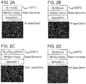
- each upper part shows a cross-sectional view of a multilayer structure of a magnetic layer and a BiSb layer
- each lower part shows a high-energy electron diffraction (RHEED) image thereof.
- a molecular beam epitaxial growth method was employed for BiSb crystal growth.
- Bi material and Sb material can be evaporated from different sources, thereby allowing the composition of Bi and Sb to be adjusted in a simple manner.
- the BiSb film may be formed by means of a sputter method using a BiSb target having a fixed composition.
- the substrate temperature is required to be set to 200°C to 250°C.
- Fig. 2A shows a structure in which a Bi layer of 10 nm is grown on a MnGa magnetic layer of 10 nm at a substrate temperature of 100°C.
- Fig. 2B shows a structure in which a Bi layer of 30 nm is grown on a MnGa magnetic layer of 10 nm at a substrate temperature of 200°C.
- Fig. 2C shows a structure in which a BiSb layer of 20 nm is grown on a MnGa magnetic layer of 10 nm at a substrate temperature of 250°C.
- Fig. 2D shows a structure in which a Sb layer of 20 nm is grown on a MnGa magnetic layer of 10 nm at a substrate temperature of 250°C.
- the growth rate is set to 2nm/min.
- RHEED was measured when the film thickness reached 2 nm.
- Fig. 2A in a case in which the substrate temperature was 100°C, only a dark RHEED image was observed.
- Fig. 2B in a case in which the substrate temperature was 200°C, a clear streak RHEED image was observed.
- Figs. 2C and 2D in a case in which the film was formed at a substrate temperature of 250°C, a clear streak was observed. That is to say, it has been found that high-quality BiSb was formed.
- the BiSb material has a (012) orientation. Based on the results described above, it has been found that film formation at a substrate temperature of 200°C or more provides a high-quality BiSb film formed on a magnetic metal substrate having a tetragonal crystal structure.
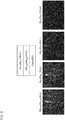
- Fig. 3 is a diagram showing a cross-sectional view (upper part) of a MnGa/BiSb multilayer structure (which is also referred to as a "MnGa/BiSb junction") according to an embodiment and the RHEED images thereof (lower part).
- a MnGa/BiSb junction which is also referred to as a "MnGa/BiSb junction”
- the RHEED images thereof lower part.
- the RHEED images were acquired after the magnetic layer (MnGa) of 3 nm was formed, and immediately after the heavy metal layer (BiSb) reached 1 nm, 5 nm, and 10 nm, respectively.
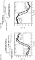
- Fig. 4 is a diagram showing the magnetic characteristics of the MnGa/BiSb multilayer structure shown in Fig. 3 .
- the BiSb layer is formed on the MnGa layer
- such a structure exhibits the same magnetic characteristics as those of a MnGa layer having a single-layer structure.
- Fig. 5 is a diagram showing an X-ray diffraction spectrum of the MnGa/BiSb multilayer structure shown in Fig. 3 .
- a BiSb layer of 20 nm was formed at a substrate temperature of 250°C after a perpendicularly magnetized MnGa magnetic thin film of 10 nm was formed. It has been found that the BiSb film formed on the MnGa layer having a tetragonal1 crystal structure has a (012) orientation.
- the MnGa magnetic film has a tetragonal crystal structure. Accordingly, it has been found that the BiSb layer formed on the MnGa magnetic film has a (012) orientation. With this structure, the lower layer having a crystal structure with fourfold symmetry (tetragonal crystal structure or cubic crystal structure) is used to provide such a (012) orientation, which greatly contributes to generating a very large spin Hall effect.
- Figs. 6A and 6B are diagrams each showing the temperature dependence of the electrical conductivity ⁇ of the BiSb thin film (having a film thickness of 10 nm) thus formed. There is a difference in the composition ratio between Figs. 6A and 6B.
- This value is one order of magnitude higher than those provided by other kinds of topological insulators such as Bi 3 Se 2 (5 ⁇ 10 4 ⁇ -1 m -1 ), (Bi,Sb) 3 Se 2 (2.2 ⁇ 10 4 ⁇ -1 m -1 ), etc., and is close to the electrical conductivity values provided by metal materials typically employed in MRAM such as Ta (5.2 ⁇ 10 5 ⁇ -1 m -1 ) or CoFeB (6 ⁇ 10 5 ⁇ -1 m -1 ), for example.
- topological insulators such as Bi 3 Se 2 (5 ⁇ 10 4 ⁇ -1 m -1 ), (Bi,Sb) 3 Se 2 (2.2 ⁇ 10 4 ⁇ -1 m -1 ), etc.
- Fig. 7 shows a cross-sectional view and a plan view of the MnGa/BiSb multilayer structure according to an example.
- the multilayer structure is configured to include a perpendicularly magnetized MnGa layer having a film thickness of 3 nm and a BiSb layer having a film thickness of 10 nm, and to have an element size of 100 ⁇ m ⁇ 50 ⁇ m.
- the magnetization of the MnGa layer is perfectly perpendicular.
- the pure spin current injected from the BiSb layer generates an effective in-plane magnetic field H SO .
- the effective in-plane magnetic field has an effect of weakening the coercive force in the perpendicular direction.
- Fig. 8A is a diagram showing magnetization hysteresis when a current flows between terminals I + and I - provided to the MnGa/BiSb multilayer structure.
- the magnetization hysteresis can be evaluated based on the measurement results of the Hall voltage that occurs due to the anomalous Hall effect that occurs between terminals V + and V - .
- the coercive force in the perpendicular direction decreases according to an increase of the in-plane current density. This reflects the effect of the effective magnetic field H SO that occurs due to the pure spin current.
- Fig. 8B is a diagram showing a relation between the reduction ⁇ H C of the coercive force in the perpendicular direction and the current density J MM that flows through the BiSb layer.
- Fig. 8B also shows data of a multilayer structure formed of a MnGa layer (3 nm) and a Ta layer (5 nm).
- the change in the coercive force per unit current density i.e., ⁇ H C /J MM
- the Ta layer is formed
- ⁇ H C /J MM is 0.35 kG/(MA/cm 2 ).
- the BiSb layer provides a very strong spin Hall effect.
- Fig. 9 shows a cross-sectional view and a plan view of a MnGa/BiSb multilayer structure according to an example.
- the multilayer structure is configured such that a BiSb layer having a thickness of 10 nm is layered on a MnGa layer having a thickness of 3 nm and having an in-plane magnetization component, which is formed as an element having a size of 100 ⁇ m ⁇ 50 ⁇ m.
- the MnGa layer has an in-plane magnetization component.
- the effective magnetic field H SO that occurs due to the pure spin current injection has a perpendicular component, thereby providing an effect of raising the coercive force.
- FIG. 10 is a diagram showing the magnetization hysteresis in the perpendicular direction when a current flows in the in-plane direction between the terminals I + and I - of the junction.
- the magnetization hysteresis in the perpendicular direction can be evaluated based on the measurement results of the Hall voltage using the anomalous Hall effect that occurs between terminals V + and V - . As shown in this drawing, it can be understood that the coercive force in the perpendicular direction rises according to an increase of the in-plane current density. This reflects the effect of the effective magnetic field H SO in the perpendicular direction.
- Figs. 11A and 11B are diagrams each showing the magnetization hysteresis in the perpendicular direction when an external magnetic field is applied as an in-plane component. With this example, the effect of the perpendicular component of the effective magnetic field H SO can be easily observed.
- Fig. 11A shows the measurement results when a positive current flowed.
- Fig. 11B shows the measurement results when a negative current flowed.
- the in-plane magnetic component in a case in which the in-plane magnetic component is a right-direction component (when the in-plane external magnetic field is applied in the positive direction), the H SO is directed upward. Accordingly, in this case, the perpendicular magnetization component is positive.
- the perpendicular component of the effective magnetic field H SO is directed downward. Accordingly, in this case, the perpendicular magnetization component is negative.
- M MnGa 250 emu/cc
- t MnGa 3nm
- the spin Hall angle can be calculated using the following Expression (2).
- ⁇ SH 2 e / h bar • J S / J BiSb
- J BiSb represents the current density that flows through the BiSb layer, which can be calculated using the following Expression (3).
- the spin Hall angle of the BiSb material is larger than that of other kinds of materials. Thus, it is considered that this allows the magnetization to be reversed using a very low current density.
- FIGs. 13A and 13B are diagrams each showing the magnetization reversal for the MnGa (3 nm)/BiSb (5 nm) junction using a pulse current.
- Fig. 13A shows the measurement result in a case in which a 100-msec pulse current was applied so as to provide magnetization reversal in a state in which an in-plane external magnetic field was applied in the left (negative) direction such that the magnetization was oriented toward the left side.
- a 100-msec pulse current was applied so as to provide magnetization reversal in a state in which an in-plane external magnetic field was applied in the left (negative) direction such that the magnetization was oriented toward the left side.
- Fig. 13B shows the measurement result in a case in which a current was applied so as to provide magnetization reversal in a state in which an in-plane external magnetic field was applied in the right (positive) direction such that the magnetization was oriented toward the right side.
- a current was applied so as to provide magnetization reversal in a state in which an in-plane external magnetic field was applied in the right (positive) direction such that the magnetization was oriented toward the right side.
- very-low-current density magnetization reversal is provided due to the very large spin Hall effect of the BiSb material.
- Figs. 14A and 14B are diagrams each showing a schematic structure of a SOT-MRAM cell 2.
- the SOT-MRAM cell 2 includes an MTJ (Magnetic Tunnel Junction) element 10, a pure spin injection source 20, a write transistor 30, and a read transistor 31.
- the MTJ element 10 has a multilayer structure including a magnetization free layer 12, a tunnel barrier 14, and a magnetization pinned layer 16.
- the pure spin injection source 20 is coupled to the magnetization free layer 12.
- a MnGa layer may be employed, for example.
- the present invention is not restricted to such an arrangement. Also, other kinds of ferromagnetic metal materials may be employed.
- Examples that can be employed as the magnetization free layer 12 include: single-element magnetic metal materials such as Co, Fe, etc.; binary alloy materials such as CoFe, NiFe, MnAI, MnGe, FePt, etc.; ternary alloy materials such as CoFeB, CoMnSi, etc.; and multilayer structures including such magnetic material layers.
- the same can be said of the magnetization pinned layer 16.
- the tunnel barrier 14 is configured as an insulating layer. MgO is preferably employed for the tunnel barrier 14. Also, other kinds of materials such as AIO may be employed.
- the pure spin injection source 20 includes the BiSb layer described above. That is to say, the junction of the magnetization free layer 12 and the pure spin injection source 20 configured as the BiSb layer can be regarded as the multilayer structure according to the example described above.
- the pure spin injection source 20 configured as the BiSb layer is coupled to an unshown power supply (driver) via the write transistor 30.
- a pulse-type current Ic flows through the BiSb layer in the in-plane direction (x direction).
- a spin current I S flows in the perpendicular direction (z direction). This causes the occurrence of magnetization reversal in the magnetization free layer 12, thereby writing data.
- Fig. 14B shows a SOT-MRAM structure obtained by geometrically reversing the structure shown in Fig. 14A .
- the BiSb layer is employed for the SOT-MRAM
- such an arrangement allows the write current and write electric power to be reduced to 1/10 times that provided by STT-MRAM.
- the SOT-MRAM is capable of writing data at a rate that is 10 times higher than that provided by the STT-MRAM. Accordingly, the SOT-MRAM employing the BiSb layer allows the data writing energy to be reduced to 1/100 times that provided by the STT-MRAM.
- this arrangement provides the wiring with improved reliability. Moreover, such an arrangement does not require the write current to directly flow through the MTJ element, thereby increasing the operating life. Furthermore, this arrangement allows the resistance of the MTJ element to be increased so as to reduce the read current, thereby allowing the read electric power to be reduced. In a case in which the write current can be reduced, this arrangement allows the size of the driving transistor to be reduced on the order of 1/10 times. This allows the degree of integration to be raised, thereby allowing the memory capacity to be increased.
- the BiSb material has the characteristic that two-dimensional current is dominant in a topological surface state.
- SOT-RAM having a perpendicular magnetization layer is provided using such a characteristic, such an arrangement can be configured as two-terminal SOT-RAM.
- Fig. 15 is a schematic diagram showing the two-terminal SOT-RAM.
- a write path is an in-plane path that differs from a read path configured as a perpendicular path.
- Such an arrangement requires three terminals, i.e., two transistors 30 and 31.
- perpendicular magnetization such an arrangement requires a bias magnetic field to be applied in the in-plane direction.
- this arrangement allows data writing using a perpendicular current path 40.
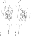
- Figs. 16A and 16B are diagrams each showing a schematic structure of a two-terminal SOT-MRAM cell 2A.
- the SOT-MRAM cell 2A includes an MTJ (Magnetic Tunnel Junction) element 10, a pure spin injection source 20, and a read/write transistor 32.
- the pure spin injection source 20 is grounded (coupled to the source line).
- the magnetization pinned layer 16 of the MnGa magnetic thin film 10 is grounded.
- the SOT-MRAM shown in Fig. 16B has a structure obtained by geometrically reversing the structure shown in Fig. 16A .
- BiSb pure spin injection source is employed in MRAM.
- the present invention is not restricted to such an application.
- the BiSb pure spin injection source can be employed in various kinds of applications that require such a pure spin injection source such as a microwave generator using precession of a magnetic layer.
- the present invention is applicable to magnetoresistive memory.
Landscapes
- Engineering & Computer Science (AREA)
- Manufacturing & Machinery (AREA)
- Computer Hardware Design (AREA)
- Hall/Mr Elements (AREA)
- Mram Or Spin Memory Techniques (AREA)
Abstract

Description
- The present invention relates to magnetoresistive memory.
- In recent years, nonvolatile memory having an advantage of low power consumption is being intensively developed. In particular, magnetoresistive memory (MRAM) is very promising. In addition to a nonvolatile memory function, MRAM exhibits very favorable properties such as 10-ns order high-speed operation, and dramatically improved memory writing durability (ensuring a number of write operations of 1016 or more). Accordingly, in a case in which such MRAM is employed as nonvolatile memory built into an integrated circuit in addition to employing it as main memory, it is anticipated that, by using the power gating effect, such an arrangement is capable of providing a 90 percent reduction in power consumption by the integrated circuit.
- Each memory element (MTJ; magnetic tunnel junction) of first-generation MRAM employs a magnetization reversal method using a magnetic field. However, the magnetization reversal using the magnetic field has a problem of large energy consumption. As the second-generation writing technique developed in the 2000s, the spin injection magnetization reversal method was researched and developed, and was put to practical use in around 2012. In the spin injection magnetization reversal technique, a spin polarization current is injected from a magnetization pinned layer to a magnetization free layer included in the MTJ element so as to cause magnetic reversal due to the spin transfer torque (STT). MRAM employing this technique is known as so-called STT-MRAM. In order to cause the spin injection magnetization reversal, a spin current Is represented by the following Expression is injected in the form of the spin polarization current. The spin current Is represents the flow of the spin angular momentum per unit time.

- hbar: Plank's constant
- e: elementary charge
- I: current
- P: spin polarization of the magnetic electrode material
- The upper limit of P is defined as 1. Typical materials have a spin polarization on the order of 0.5. As can be understood from this Expression, in the spin injection magnetization reversal technique, the spin current does not exceed (hbar/2e) • I. This is because there is a physical limit in that each electron can only transfer a spin angular momentum of hbar/2. MRAM is configured as nonvolatile memory. Accordingly, in the standby state, MRAM does not consume power. However, MRAM still has a problem of energy consumption that is an order of magnitude larger than other kinds of memory such as SRAM or the like. Furthermore, in order to provide a large write current, a large driving transistor is required. Accordingly, it is difficult to increase the capacity of MRAM.
-
Fig. 1 is a schematic diagram for explaining a magnetization reversal method using a pure spin current. A ferromagnetic layer is coupled to a material having a strong spin-orbit interaction. When a current I flows through such a material layer, a pure spin current Is flows in the perpendicular direction. Such a phenomenon is known as the spin Hall effect. There is a relation between the pure spin current density Js and the current density J, which is represented by Js = (hbar/2e) • θsh • J. Here, θsh represents a parameter that reflects the strength of the spin orbit interaction, which is referred to as the spin Hall angle. Accordingly, the following relation holds true between the pure spin current Is and the current I.
- That is to say, substantially, such an arrangement allows each electron to generate a spin of (L/tN) • θsh. It can be understood that, if (L/tN) • θsh >> 1, such an arrangement using a pure spin current provides magnetization reversal with higher efficiency than that provided by an arrangement employing ordinary spin injection magnetization reversal. Typically, (L/tN) is in a range between 5 and 10. Accordingly, in a case in which a spin Hall material having a θsh that is larger than 1 is employed, this arrangement allows the current and electric power required for the occurrence of magnetization reversal in the MRAM element to be reduced by an order of magnitude. Furthermore, the pure spin current injection magnetization reversal method provides magnetization reversal with higher speed by approximately one order of magnitude. Such an arrangement allows the writing energy to be reduced by two orders of magnitude. Such MRAM using pure spin current injection based on the spin Hall effect is known as spin-orbit-torque (SOT) MRAM.
-
- [Non-patent document 1]
"Conversion of pure spin current to charge current in amorphous bismuth", J. Appl. Phys. 115, 17C507 (2014). - [Non-patent document 2]
"Transport and spin conversion of multicarriers in semimetal bismuth", Phys. Rev. B 93,174428 (2016). - [Non-patent document 3]
"Tunable Giant Spin Hall Conductivities in a Strong Spin-Orbit Semimetal: Bi1-xSbx", Phys. Rev. Lett. 114, 107201 (2015). - As spin Hall materials, Pt, W, Ta, and the like, which are heavy metal materials, have been researched. Such materials are each a metal material. Accordingly, such materials each have high electrical conductivity on the order of 105 Ω-1m-1, but has an unsatisfactory θsh on the order of 0.1. In contrast, a topological insulator, which has attracted attention in recent years, has a very high θsh ranging between 2 and 3. However, a topological insulator has a low electrical conductivity on the order of 103 and 104 Ω-1m-1. Accordingly, in a case in which such a topological insulator is employed in MRAM, very little current flows through the topological insulator and most current flows through the other metal layers, which is impractical.
- The present invention has been made in view of such a situation. Accordingly, it is an exemplary purpose of an embodiment of the present invention to provide a spin Hall material having a large spin Hall angle and magnetoresistive memory employing such a spin Hall material.
- An embodiment of the present invention relates to magnetoresistive memory. The magnetoresistive memory comprises: an MTJ (magnetic tunnel junction) element comprising a magnetization free layer; and a pure spin injection source comprising a BiSb layer coupled to the magnetization free layer. The magnetoresistive memory is structured to flow an in-plane current through the BiSb layer so as to provide magnetization reversal of the magnetization free layer.
- With this embodiment, write current and write electric power can be reduced.
- Also, the BiSb layer may be structured as a crystalized layer. With such an arrangement in which the BiSb layer is formed as a crystalized layer, this arrangement provides the BiSb layer with a very large spin Hall angle, thereby providing the magnetoresistive memory with further improved performance.
- Another embodiment of the present invention relates to a manufacturing method for magnetoresistive memory. The manufacturing method comprises: forming a magnetization free layer; and forming a pure spin injection source comprising a BiSb layer. The BiSb layer is formed at a substrate temperature of 200 to 250°C.
- Yet another embodiment of the present invention relates to a manufacturing method for a multilayer structure of a magnetic body and a BiSb layer. The BiSb layer is formed at a substrate temperature of 200 to 250°C.
- In a case in which the BiSb layer is formed under this condition, a BiSb layer having high-quality crystallinity can be formed. This provides a spin Hall material having a large spin angle.
- With an embodiment of the present invention, a spin Hall material is provided with a large spin angle.
-
-
Fig. 1 is a schematic diagram for explaining a magnetization reversal method using a pure spin current; - In
Figs. 2A through 2D , each upper part shows a cross-sectional view of a multilayer structure of a magnetic layer and a BiSb layer, and each lower part shows a high-energy electron diffraction (RHEED) image thereof; -
Fig. 3 shows a cross-sectional view of a MnGa/BiSb multilayer structure according to an embodiment (upper part) and an RHEED image (lower part); -
Fig. 4 is a diagram showing the magnetic characteristics of the MnGa/BiSb multilayer structure shown inFig. 3 ; -
Fig. 5 is a diagram showing an X-ray diffraction spectrum of the MnGa/BiSb multilayer structure shown inFig. 3 ; and -
Figs. 6A and 6B are diagrams each showing the temperature dependence of the electrical conductivity σ of the BiSb thin film (having a film thickness of 10 nm) thus formed. -
Fig. 7 shows a cross-sectional view and a plan view of a MnGa/BiSb multilayer structure according to an embodiment; -
Fig. 8A is a diagram showing a magnetization hysteresis when a current flows between terminals I+ and I- provided to the MnGa/BiSb multilayer structure, andFig. 8B is a diagram showing a relation between the change in the coercive force that occurs in the MnGa layer in the perpendicular direction and the current density JMM that flows through the BiSb layer; -
Fig. 9 shows a cross-sectional view and a plan view of a MnGa/BiSb multilayer structure according to an example; -
Fig. 10 is a diagram showing the magnetization hysteresis in the perpendicular direction when a current flows in the in-plane direction between the terminals I+ and I- of the junction; -
Figs. 11A and 11B are diagrams each showing the magnetization hysteresis in the perpendicular direction when an external magnetic field is applied as an in-plane component to the same sample as that shown inFig. 9 ; -
Fig. 12 is a diagram showing the spin Hall angle θsh at room temperature, the electrical conductivity σ, and the spin Hall conductivity σsh for each material of the pure spin injection source; -
Figs. 13A and 13B are diagrams each showing the magnetization reversal for the MnGa (3 nm)/BiSb (5 nm) junction using a pulse current; -
Figs. 14A and 14B are diagrams each showing a schematic structure of a SOT-MRAM cell; -
Fig. 15 is a schematic diagram showing a two-terminal SOT-RAM; and -
Figs. 16A and 16B are diagrams each showing a schematic structure of a two-terminal SOT-MRAM cell. - In the present disclosure, description will be made directing attention to a BiSb material, which has both the high conductivity of a heavy metal material and the large spin Hall angle of a topological insulator. The BiSb material has been known as a conventional material. However, research on the BiSb material has been limited to research on amorphous BiSb. For example, as prior research, several reports are known with respect to a Bi layer formed on a NiFe substrate. The spin Hall angle θsh provided by the amorphous Bi layer evaluated in these reports is only 0.02 (Non-patent document 1) or only 0.00012 (Non-patent document 2), which is very small. Furthermore, such an arrangement has the potential to have a dead layer configured as a non-magnetic layer on the interface between the BiSb layer and a magnetic layer, which drastically degrades the magnetic characteristics of the magnetic layer. This has also been a disincentive to further research.
- The performance of the spin Hall effect is represented by an index which is called spin Hall conductivity, calculated as the product of the electrical conductivity σ and the spin Hall angle θsh, i.e., represented by σsh = (hbar/2e) • σ × θsh. However, in a theoretical calculation, a crystallized BiSb material has σsh of only 4.9 × 10⁴ • (hbar/2e) Ω-1m-1 at maximum (Non-patent document 3). Accordingly, it has been believed that the BiSb material provides a θsh on the order of only 0.5 at maximum.
- Based on these reports, it has been considered that BiSb material has no potential to provide a large spin Hall angle. It is a fact that there has been no research following the prior research.
- Despite the negative results obtained in the prior research, the present inventors have considered that, if a high-quality crystalized BiSb material is formed on a magnetic metal material, such an arrangement has the potential to provide both high electrical conductivity and a high spin Hall angle. Such an arrangement that supports both the advantages described above has the potential to become a great breakthrough for developing magnetoresistive memory.
- Description will be made regarding a film forming method for forming a BiSb film on a magnetic material, and regarding evaluation results of the pure spin injection magnetization reversal performance provided by the BiSb film thus formed.
- A BiSb alloy material has a hexagonal crystal structure. In contrast, most kinds of magnetic metal materials employed in MRAM have a tetragonal crystal structure. Accordingly, it was not known if a high-quality crystalized BiSb film could be formed on such a magnetic metal layer. Accordingly, first, film forming conditions for forming a BiSb film on a magnetic material were researched.
- In
Figs. 2A through 2D , each upper part shows a cross-sectional view of a multilayer structure of a magnetic layer and a BiSb layer, and each lower part shows a high-energy electron diffraction (RHEED) image thereof. - A molecular beam epitaxial growth method (MBE method) was employed for BiSb crystal growth. In this method, Bi material and Sb material can be evaporated from different sources, thereby allowing the composition of Bi and Sb to be adjusted in a simple manner. However, in a case in which there is no need to adjust the BiSb composition in particular from that fixed beforehand, the BiSb film may be formed by means of a sputter method using a BiSb target having a fixed composition. In order to provide a high-quality BiSb crystalized film using the MBE method or the sputter method, the substrate temperature is required to be set to 200°C to 250°C.
-
Fig. 2A shows a structure in which a Bi layer of 10 nm is grown on a MnGa magnetic layer of 10 nm at a substrate temperature of 100°C.Fig. 2B shows a structure in which a Bi layer of 30 nm is grown on a MnGa magnetic layer of 10 nm at a substrate temperature of 200°C.Fig. 2C shows a structure in which a BiSb layer of 20 nm is grown on a MnGa magnetic layer of 10 nm at a substrate temperature of 250°C.Fig. 2D shows a structure in which a Sb layer of 20 nm is grown on a MnGa magnetic layer of 10 nm at a substrate temperature of 250°C. In each case, the growth rate is set to 2nm/min. RHEED was measured when the film thickness reached 2 nm. - As shown in
Fig. 2A , in a case in which the substrate temperature was 100°C, only a dark RHEED image was observed. As shown inFig. 2B , in a case in which the substrate temperature was 200°C, a clear streak RHEED image was observed. Also, as shown inFigs. 2C and 2D , in a case in which the film was formed at a substrate temperature of 250°C, a clear streak was observed. That is to say, it has been found that high-quality BiSb was formed. Furthermore, based on X-ray analysis results, it has been found that the BiSb material has a (012) orientation. Based on the results described above, it has been found that film formation at a substrate temperature of 200°C or more provides a high-quality BiSb film formed on a magnetic metal substrate having a tetragonal crystal structure. -
Fig. 3 is a diagram showing a cross-sectional view (upper part) of a MnGa/BiSb multilayer structure (which is also referred to as a "MnGa/BiSb junction") according to an embodiment and the RHEED images thereof (lower part). In this example, first, after a perpendicularly magnetized MnGa magnetic thin film of 3 nm was formed, a Bi0.9Sb0.1 of 10 nm was formed. The RHEED images were acquired after the magnetic layer (MnGa) of 3 nm was formed, and immediately after the heavy metal layer (BiSb) reached 1 nm, 5 nm, and 10 nm, respectively. Very clear streak diffraction images were observed at an interface between the MnGa layer and the BiSb layer. As the film thickness of the BiSb layer became larger, the RHEED image intensity became lower, but did not become zero. Based on the results described above, it has been found that a dramatically flat interface having no segregation was obtained between the MnGa layer and the BiSb layer. -
Fig. 4 is a diagram showing the magnetic characteristics of the MnGa/BiSb multilayer structure shown inFig. 3 . In a case in which the BiSb layer is formed on the MnGa layer, such a structure exhibits the same magnetic characteristics as those of a MnGa layer having a single-layer structure. Thus, it has been found that there is no magnetic dead layer at the interface between the MnGa layer and the BiSb layer. -
Fig. 5 is a diagram showing an X-ray diffraction spectrum of the MnGa/BiSb multilayer structure shown inFig. 3 . As the measurement target, a BiSb layer of 20 nm was formed at a substrate temperature of 250°C after a perpendicularly magnetized MnGa magnetic thin film of 10 nm was formed. It has been found that the BiSb film formed on the MnGa layer having a tetragonal1 crystal structure has a (012) orientation. - Furthermore, as shown in
Fig. 5 , the MnGa magnetic film has a tetragonal crystal structure. Accordingly, it has been found that the BiSb layer formed on the MnGa magnetic film has a (012) orientation. With this structure, the lower layer having a crystal structure with fourfold symmetry (tetragonal crystal structure or cubic crystal structure) is used to provide such a (012) orientation, which greatly contributes to generating a very large spin Hall effect. -
Figs. 6A and 6B are diagrams each showing the temperature dependence of the electrical conductivity σ of the BiSb thin film (having a film thickness of 10 nm) thus formed. There is a difference in the composition ratio betweenFigs. 6A and 6B. Fig. 6A shows the characteristics of a Bi0.92Sb0.08 sample. At room temperature, σBiSb = 3.8 × 10⁵ Ω-1m-1 was obtained. Furthermore, the electrical conductivity σ rises according to a reduction in the temperature. Thus, it has been found that this sample has metallic electrical conductivity characteristics. - On the other hand,
Fig. 6B shows the characteristics of a Bi0.89Sb0.11 sample. This sample exhibits low electrical conductivity. However, at room temperature, σBiSb = 1.1 × 10⁵ Ω-1m-1 was obtained. The electrical conductivity of a BiSb thin film having a film thickness of 10 nm was 1 × 10⁵ Ω-1m-1 to 4 × 10⁵ Ω-1m-1, and σBiSb ∼ 2.5 × 10⁵ Ω-1m-1 was obtained as an average value. This value is one order of magnitude higher than those provided by other kinds of topological insulators such as Bi3Se2 (5 × 10⁴ Ω-1m-1), (Bi,Sb)3Se2 (2.2 × 10⁴ Ω-1m-1), etc., and is close to the electrical conductivity values provided by metal materials typically employed in MRAM such as Ta (5.2 × 10⁵ Ω-1m-1) or CoFeB (6 × 10⁵ Ω-1m-1), for example. - Next, description will be made regarding the evaluation results of the spin Hall angle of the BiSb layer.
Fig. 7 shows a cross-sectional view and a plan view of the MnGa/BiSb multilayer structure according to an example. The multilayer structure is configured to include a perpendicularly magnetized MnGa layer having a film thickness of 3 nm and a BiSb layer having a film thickness of 10 nm, and to have an element size of 100 µm × 50 µm. In this example, the magnetization of the MnGa layer is perfectly perpendicular. Accordingly, the pure spin current injected from the BiSb layer generates an effective in-plane magnetic field HSO. The effective in-plane magnetic field has an effect of weakening the coercive force in the perpendicular direction. -
Fig. 8A is a diagram showing magnetization hysteresis when a current flows between terminals I+ and I- provided to the MnGa/BiSb multilayer structure. The magnetization hysteresis can be evaluated based on the measurement results of the Hall voltage that occurs due to the anomalous Hall effect that occurs between terminals V+ and V-. As shown in this drawing, it can be understood that the coercive force in the perpendicular direction decreases according to an increase of the in-plane current density. This reflects the effect of the effective magnetic field HSO that occurs due to the pure spin current. -
Fig. 8B is a diagram showing a relation between the reduction ΔHC of the coercive force in the perpendicular direction and the current density JMM that flows through the BiSb layer. As reference data,Fig. 8B also shows data of a multilayer structure formed of a MnGa layer (3 nm) and a Ta layer (5 nm). As can be understood from this drawing, in a case in which the BiSb layer is formed, the change in the coercive force per unit current density, i.e., ΔHC/JMM, is 3.7 kG/(MA/cm2). In contrast, in a case in which the Ta layer is formed, ΔHC/JMM is 0.35 kG/(MA/cm2). As can be understood from this comparison result, the BiSb layer provides a very strong spin Hall effect. - As described above, in the prior research, when the spin Hall angle of an amorphous Bi layer on a magnetic layer was evaluated, the spin Hall angle was very small, that is, θsh = 0.02 or 0.00012 (
Non-patent documents 1, 2). Furthermore, the σsh of the BiSb layer obtained from the theoretical calculation was only on the order of 4.9 × 10⁴ Ω-1m-1 at maximum. Accordingly, it was considered that the BiSb layer provides a spin Hall angle θsh on the order of only 0.5 at maximum. -
Fig. 9 shows a cross-sectional view and a plan view of a MnGa/BiSb multilayer structure according to an example. The multilayer structure is configured such that a BiSb layer having a thickness of 10 nm is layered on a MnGa layer having a thickness of 3 nm and having an in-plane magnetization component, which is formed as an element having a size of 100 µm × 50 µm. With this example, the MnGa layer has an in-plane magnetization component. The effective magnetic field HSO that occurs due to the pure spin current injection has a perpendicular component, thereby providing an effect of raising the coercive force.Fig. 10 is a diagram showing the magnetization hysteresis in the perpendicular direction when a current flows in the in-plane direction between the terminals I+ and I- of the junction. The magnetization hysteresis in the perpendicular direction can be evaluated based on the measurement results of the Hall voltage using the anomalous Hall effect that occurs between terminals V+ and V-. As shown in this drawing, it can be understood that the coercive force in the perpendicular direction rises according to an increase of the in-plane current density. This reflects the effect of the effective magnetic field HSO in the perpendicular direction. -
Figs. 11A and 11B are diagrams each showing the magnetization hysteresis in the perpendicular direction when an external magnetic field is applied as an in-plane component. With this example, the effect of the perpendicular component of the effective magnetic field HSO can be easily observed. -
Fig. 11A shows the measurement results when a positive current flowed.Fig. 11B shows the measurement results when a negative current flowed. InFig. 11A , in a case in which the in-plane magnetic component is a right-direction component (when the in-plane external magnetic field is applied in the positive direction), the HSO is directed upward. Accordingly, in this case, the perpendicular magnetization component is positive. Conversely, in a case in which the in-plane magnetic component is a left-direction component (when the in-plane external magnetic field is applied in the negative direction), the perpendicular component of the effective magnetic field HSO is directed downward. Accordingly, in this case, the perpendicular magnetization component is negative. - In the case shown in
Fig. 11B , for a current to flow in the reverse direction, the pure spin current is injected in the reverse direction. In this case, the perpendicular component of the effective magnetic field HSO and the perpendicular magnetic component have opposite behaviors with respect to those shown inFig. 11A . Based on the results, the pure spin current injection effect by means of the BiSb layer has been confirmed. - Next, quantitative evaluation of the magnitude of the spin Hall effect is performed. In
Fig. 10 , the change in the coercive force ΔHC itself corresponds to HSO. That is to say, HSO = ΔHCO holds true. With the present invention, the pure spin current can be calculated using the following Expression (1).
- Here, MMnGa (= 250 emu/cc) represents the magnetization of the MnGa. tMnGa (= 3nm) represents the thickness of the MnGa magnetic layer. Furthermore, the spin Hall angle can be calculated using the following Expression (2).

- Here, JBiSb represents the current density that flows through the BiSb layer, which can be calculated using the following Expression (3).

- For example, in a case in which σBiSb = 2.5 × 10⁵ Ω-1m-1, σMnGa = 5 × 10⁵ Ω-1m-1, tMnGa = 3 nm, and tBiSb = 10 nm, when J = 1.38 × 10⁶ A/cm2, JBiSb = 1.12 × 10⁶ A/cm2 is obtained. On the other hand, this current density generates HSO = ΔHC = 3.1 kOe = 3100 Oe. This provides HSO/JBiSb = 2770 Oe/(MA/cm2). It can be understood that this value is several hundred times larger than the corresponding values of 5 to 10 Oe/(A/cm2) of conventionally researched heavy metal materials such as Ta or Pt. In a case in which the spin Hall angle of BiSb is calculated in actuality for each current value using Expressions (1) and (2), θsh = 52 is obtained as the average value of the spin Hall angle. This value is dramatically larger than those of a Ta layer (θsh = 0.15) or a Pt layer (θsh = 0.08) which are typically employed for MRAM. This value is approximately 100 times larger than the theoretically calculated value θsh = 0.5. Thus, it is thought that there is another mechanism that differs from the mechanism assumed in the theoretical calculation, which contributes to such a dramatically large spin Hall effect provided by the BiSb layer.
-
Fig. 12 is a diagram showing the spin Hall angle θsh at room temperature, the electrical conductivity σ, and the spin Hall conductivity σsh = (hbar/2e) • θsh × σ for each material of the pure spin injection source. Based on the comparison results, it can be understood that the BiSb material provides overwhelmingly large spin Hall conductivity 1.3 × 10⁷ (hbar/2e) Ω-1m-1. This value is 200 times or more larger than the prediction value of the theoretical calculation, i.e., 4.9 × 10⁴ (hbar/2e) Ω-1m-1. - As can be understood from
Fig. 12 , the spin Hall angle of the BiSb material is larger than that of other kinds of materials. Thus, it is considered that this allows the magnetization to be reversed using a very low current density. - Magnetization reversal using a very low current density was performed for the MnGa/BiSb junction.
Figs. 13A and 13B are diagrams each showing the magnetization reversal for the MnGa (3 nm)/BiSb (5 nm) junction using a pulse current. Specifically,Fig. 13A shows the measurement result in a case in which a 100-msec pulse current was applied so as to provide magnetization reversal in a state in which an in-plane external magnetic field was applied in the left (negative) direction such that the magnetization was oriented toward the left side. As can be understood from this drawing, upon raising the positive current, the magnetization is reversed from upward to downward. Conversely, upon raising the negative current, the magnetization is reversed from downward to upward. -
Fig. 13B shows the measurement result in a case in which a current was applied so as to provide magnetization reversal in a state in which an in-plane external magnetic field was applied in the right (positive) direction such that the magnetization was oriented toward the right side. As can be understood from this drawing, upon raising the positive current, the magnetization is reversed from downward to upward. Conversely, upon raising the negative current, the magnetization is reversed from upward to downward. That is to say, in a case of reversing the direction of the magnetization, the direction of the magnetization reversal is reversed according to the direction in which the magnetization is oriented. This measurement result is consistent with the characteristics of pure spin injection magnetization reversal. - Furthermore, it should be noted that the magnetization reversal requires only a very small current density J = 1.5 × 10⁶ A/cm2. As a comparison example, a MnGa(3 nm)/Ta(5 nm) junction requires J = 1.1 × 10⁸ A/cm2 to provide magnetization reversal. Also, a MnGa(3 nm)/IrMn(4 nm) junction requires J = 1.5 × 10⁸ A/cm2 to provide magnetization reversal. Also, a MnGa(2.5 nm)/Pt(2 nm) junction requires J = 5.0 × 10⁷ A/cm2 to provide magnetization reversal. In this example, it has been confirmed that very-low-current density magnetization reversal is provided due to the very large spin Hall effect of the BiSb material.
-
Figs. 14A and 14B are diagrams each showing a schematic structure of a SOT-MRAM cell 2. Referring toFig. 14A , the SOT-MRAM cell 2 includes an MTJ (Magnetic Tunnel Junction)element 10, a purespin injection source 20, awrite transistor 30, and aread transistor 31. TheMTJ element 10 has a multilayer structure including a magnetizationfree layer 12, atunnel barrier 14, and a magnetization pinnedlayer 16. The purespin injection source 20 is coupled to the magnetizationfree layer 12. As the magnetizationfree layer 12, a MnGa layer may be employed, for example. However, the present invention is not restricted to such an arrangement. Also, other kinds of ferromagnetic metal materials may be employed. Examples that can be employed as the magnetizationfree layer 12 include: single-element magnetic metal materials such as Co, Fe, etc.; binary alloy materials such as CoFe, NiFe, MnAI, MnGe, FePt, etc.; ternary alloy materials such as CoFeB, CoMnSi, etc.; and multilayer structures including such magnetic material layers. The same can be said of the magnetization pinnedlayer 16. Thetunnel barrier 14 is configured as an insulating layer. MgO is preferably employed for thetunnel barrier 14. Also, other kinds of materials such as AIO may be employed. - The pure
spin injection source 20 includes the BiSb layer described above. That is to say, the junction of the magnetizationfree layer 12 and the purespin injection source 20 configured as the BiSb layer can be regarded as the multilayer structure according to the example described above. - The pure
spin injection source 20 configured as the BiSb layer is coupled to an unshown power supply (driver) via thewrite transistor 30. Upon turning on thewrite transistor 30, a pulse-type current Ic flows through the BiSb layer in the in-plane direction (x direction). In this state, a spin current IS flows in the perpendicular direction (z direction). This causes the occurrence of magnetization reversal in the magnetizationfree layer 12, thereby writing data. -
Fig. 14B shows a SOT-MRAM structure obtained by geometrically reversing the structure shown inFig. 14A . - Lastly, description will be made regarding the performance of the SOT-MRAM employing the BiSb layer. Description will be made assuming that a cp37nm MRAM element manufactured by TDK Corporation is employed as an example. In a case in which a BiSb layer having a thickness of 5 nm is employed as the pure spin injection source, a current of 2.2 µA is required to cause the occurrence of magnetization reversal in the cp37nm MRAM element. In contrast, with a conventional spin injection magnetization reversal method, current of 24 µA is required to cause the occurrence of magnetization reversal. Accordingly, in a case in which the BiSb layer is employed for the SOT-MRAM, such an arrangement allows the write current and write electric power to be reduced to 1/10 times that provided by STT-MRAM. Furthermore, the SOT-MRAM is capable of writing data at a rate that is 10 times higher than that provided by the STT-MRAM. Accordingly, the SOT-MRAM employing the BiSb layer allows the data writing energy to be reduced to 1/100 times that provided by the STT-MRAM.
- Furthermore, in a case in which the write current can be reduced, this arrangement provides the wiring with improved reliability. Moreover, such an arrangement does not require the write current to directly flow through the MTJ element, thereby increasing the operating life. Furthermore, this arrangement allows the resistance of the MTJ element to be increased so as to reduce the read current, thereby allowing the read electric power to be reduced. In a case in which the write current can be reduced, this arrangement allows the size of the driving transistor to be reduced on the order of 1/10 times. This allows the degree of integration to be raised, thereby allowing the memory capacity to be increased.
- The BiSb material has the characteristic that two-dimensional current is dominant in a topological surface state. In a case in which SOT-RAM having a perpendicular magnetization layer is provided using such a characteristic, such an arrangement can be configured as two-terminal SOT-RAM.
-
Fig. 15 is a schematic diagram showing the two-terminal SOT-RAM. With typical SOT-RAM, as shown inFig. 14 , a write path is an in-plane path that differs from a read path configured as a perpendicular path. Such an arrangement requires three terminals, i.e., twotransistors Fig. 15 , this arrangement allows data writing using a perpendicularcurrent path 40. This is because such an arrangement requires only a current that flows in the perpendicular direction to provide an in-plane current 42 in the BiSb layer, thereby injecting a pure spin current using the spin Hall effect. As a result, asingle transistor 32 functions as both a read transistor and a write transistor, thereby allowing the SOT-RAM to be configured as a two-terminal SOT-RAM. Furthermore, a current flows in the device in the perpendicular direction, thereby providing the spin transfer torque effect. This arrangement provides magnetic reversal without a need to apply the in-plane bias magnetic field. -
Figs. 16A and 16B are diagrams each showing a schematic structure of a two-terminal SOT-MRAM cell 2A. Referring toFig. 16A , the SOT-MRAM cell 2A includes an MTJ (Magnetic Tunnel Junction)element 10, a purespin injection source 20, and a read/write transistor 32. In the SOT-MRAM 2 shown inFigs. 14A and 14B , the purespin injection source 20 is grounded (coupled to the source line). In contrast, inFigs. 16A and 16B , the magnetization pinnedlayer 16 of the MnGa magneticthin film 10 is grounded. The SOT-MRAM shown inFig. 16B has a structure obtained by geometrically reversing the structure shown inFig. 16A . - Description has been made in the embodiment regarding an example in which the BiSb pure spin injection source is employed in MRAM. However, the present invention is not restricted to such an application. Also, the BiSb pure spin injection source can be employed in various kinds of applications that require such a pure spin injection source such as a microwave generator using precession of a magnetic layer.
- 2 cell, 10 MTJ element, 12 magnetization free layer, 14 tunnel barrier, 16 magnetization pinned layer, 20 pure spin injection source, 30 write transistor.
- The present invention is applicable to magnetoresistive memory.
Claims (11)
- Magnetoresistive memory comprising:an MTJ (magnetic tunnel junction) element comprising a magnetization free layer; anda pure spin injection source comprising a BiSb layer coupled to the magnetization free layer,wherein the magnetoresistive memory is structured to flow an in-plane current through the BiSb layer so as to provide magnetization reversal of the magnetization free layer.
- The magnetoresistive memory according to claim 1, wherein the BiSb layer is structured as a crystalized layer.
- The magnetoresistive memory according to claim 1 or 2, wherein the BiSb layer has a (012) orientation.
- The magnetoresistive memory according to any one of claims 1 through 3, wherein each cell is structured to have two terminals by using a topological surface state of the BiSb layer.
- The magnetoresistive memory according to claim 4, structured to operate without application of an in-plane bias magnetic field.
- A manufacturing method for magnetoresistive memory, comprising:forming a magnetization free layer; andforming a pure spin injection source comprising a BiSb layer,wherein the BiSb layer is formed at a substrate temperature of 200 to 250°C.
- A manufacturing method for a multilayer structure of a magnetic body and a BiSb layer, wherein the BiSb layer is formed at a substrate temperature of 200 to 250°C.
- The manufacturing method according to claim 6 or 7, wherein the BiSb layer has a (012) orientation.
- A pure spin injection source structured to inject a pure spin current to a magnetic body,
wherein the pure spin injection source comprises a BiSb layer coupled to the magnetic body,
and wherein a pure spin current is supplied to the magnetic body in a perpendicular direction according to an in-plane current that flows through the BiSb layer. - The pure spin injection source according to claim 9, wherein the BiSb layer is structured as a crystalized layer.
- Magnetoresistive memory comprising:an MTJ (magnetic tunnel junction) element comprising a magnetization free layer; anda pure spin injection source comprising a BiSb layer coupled to the magnetization free layer,wherein the BiSb layer has a (012) orientation so as to allow a lower layer having a crystal structure with fourfold symmetry to be employed.
Applications Claiming Priority (2)
| Application Number | Priority Date | Filing Date | Title |
|---|---|---|---|
| JP2017177564 | 2017-09-15 | ||
| PCT/JP2018/034191 WO2019054484A1 (en) | 2017-09-15 | 2018-09-14 | METHOD FOR MANUFACTURING LAYERED STRUCTURE OF MAGNETIC BODY AND BiSb, MAGNETORESISTIVE MEMORY, AND PURE SPIN INJECTION SOURCE |
Publications (4)
| Publication Number | Publication Date |
|---|---|
| EP3683829A1 true EP3683829A1 (en) | 2020-07-22 |
| EP3683829A4 EP3683829A4 (en) | 2021-06-02 |
| EP3683829B1 EP3683829B1 (en) | 2025-08-27 |
| EP3683829B8 EP3683829B8 (en) | 2025-10-08 |
Family
ID=65723310
Family Applications (1)
| Application Number | Title | Priority Date | Filing Date |
|---|---|---|---|
| EP18856532.9A Active EP3683829B8 (en) | 2017-09-15 | 2018-09-14 | Pure spin injection source based on bisb layer and magnetoresistive memory including the same |
Country Status (6)
| Country | Link |
|---|---|
| US (1) | US11637234B2 (en) |
| EP (1) | EP3683829B8 (en) |
| JP (1) | JP7227614B2 (en) |
| KR (1) | KR102545571B1 (en) |
| CN (1) | CN111095530B (en) |
| WO (1) | WO2019054484A1 (en) |
Cited By (1)
| Publication number | Priority date | Publication date | Assignee | Title |
|---|---|---|---|---|
| KR20230074366A (en) * | 2021-11-19 | 2023-05-30 | 삼성전자주식회사 | Semiconductor memory device |
Families Citing this family (24)
| Publication number | Priority date | Publication date | Assignee | Title |
|---|---|---|---|---|
| KR102518015B1 (en) * | 2019-01-31 | 2023-04-05 | 삼성전자주식회사 | A magnetoresistive random access device memory and method of manufacturing the same |
| KR102251067B1 (en) * | 2019-05-28 | 2021-05-14 | 서울대학교산학협력단 | Magnetic memory device and operating method thereof |
| JP2021057357A (en) * | 2019-09-26 | 2021-04-08 | 国立大学法人東京工業大学 | Magnetoresistive memory |
| US11694713B2 (en) | 2020-02-12 | 2023-07-04 | Western Digital Technologies, Inc. | BiSb topological insulator with novel buffer layer that promotes a BiSb (012) orientation |
| US11489108B2 (en) * | 2020-04-28 | 2022-11-01 | Western Digital Technologies, Inc. | BiSb topological insulator with seed layer or interlayer to prevent sb diffusion and promote BiSb (012) orientation |
| US11495741B2 (en) * | 2020-06-30 | 2022-11-08 | Western Digital Technologies, Inc. | Bismuth antimony alloys for use as topological insulators |
| US11100946B1 (en) | 2020-07-01 | 2021-08-24 | Western Digital Technologies, Inc. | SOT differential reader and method of making same |
| US11094338B1 (en) | 2020-07-09 | 2021-08-17 | Western Digital Technologies, Inc. | SOT film stack for differential reader |
| US12213387B2 (en) * | 2020-07-27 | 2025-01-28 | Samsung Electronics Co., Ltd. | Spin-orbit torque structure including topological materials and magnetic memory device including the spin-orbit torque structure |
| KR102361064B1 (en) * | 2020-11-06 | 2022-02-14 | 한국과학기술원 | Magnetic Device With Gate Electrode |
| US11521665B2 (en) * | 2021-05-04 | 2022-12-06 | Nxp Usa, Inc. | Non-volatile memory having write detect circuitry |
| US11763973B2 (en) * | 2021-08-13 | 2023-09-19 | Western Digital Technologies, Inc. | Buffer layers and interlayers that promote BiSbx (012) alloy orientation for SOT and MRAM devices |
| US11532323B1 (en) | 2021-08-18 | 2022-12-20 | Western Digital Technologies, Inc. | BiSbX (012) layers having increased operating temperatures for SOT and MRAM devices |
| JP7614589B2 (en) | 2021-08-31 | 2025-01-16 | 国立大学法人東京科学大学 | Spin injection source, magnetic memory, spin Hall oscillator, and computer |
| US11823723B2 (en) * | 2021-11-22 | 2023-11-21 | International Business Machines Corporation | Memory device with spin-harvesting structure |
| CN117694031A (en) | 2021-12-22 | 2024-03-12 | 西部数据技术公司 | Novel doping process to refine grain size for smoother BiSb film surface |
| US11875827B2 (en) | 2022-03-25 | 2024-01-16 | Western Digital Technologies, Inc. | SOT reader using BiSb topological insulator |
| US11783853B1 (en) | 2022-05-31 | 2023-10-10 | Western Digital Technologies, Inc. | Topological insulator based spin torque oscillator reader |
| US12487296B2 (en) * | 2023-03-13 | 2025-12-02 | Western Digital Technologies, Inc. | Spin orbit torque based thermal sensor for insitu monitoring of magnetic recording head |
| US20240412759A1 (en) * | 2023-06-08 | 2024-12-12 | Western Digital Technologies, Inc. | Film and Method for BiSbX (012) Texture for SOT Devices |
| US12154603B1 (en) | 2023-06-14 | 2024-11-26 | Western Digital Technologies, Inc. | Spin-orbit torque (SOT) writer with topological insulator materials |
| US12354627B2 (en) | 2023-06-28 | 2025-07-08 | Western Digital Technologies, Inc. | Higher areal density non-local spin orbit torque (SOT) writer with topological insulator materials |
| US12394432B2 (en) * | 2023-06-19 | 2025-08-19 | Western Digital Technologies, Inc. | Non-localized spin valve reader hybridized with spin orbit torque layer |
| US20250246353A1 (en) * | 2024-01-31 | 2025-07-31 | Western Digital Technologies, Inc. | RuAl and MgTiO Lamination For Effective Buffer and Interlayers For Topological Material Layers |
Family Cites Families (15)
| Publication number | Priority date | Publication date | Assignee | Title |
|---|---|---|---|---|
| JPS60160015A (en) | 1984-01-31 | 1985-08-21 | Sony Corp | Magnetic recording medium |
| JPH08249875A (en) | 1995-03-14 | 1996-09-27 | Toshiba Corp | Solid-state magnetic recording element |
| JP5514059B2 (en) | 2010-09-17 | 2014-06-04 | 株式会社東芝 | Magnetoresistive element and magnetic random access memory |
| US9704793B2 (en) | 2011-01-04 | 2017-07-11 | Napra Co., Ltd. | Substrate for electronic device and electronic device |
| JP6017149B2 (en) | 2012-02-27 | 2016-10-26 | 日本放送協会 | Spin injection magnetization reversal element and magnetoresistive random access memory |
| US9076537B2 (en) * | 2012-08-26 | 2015-07-07 | Samsung Electronics Co., Ltd. | Method and system for providing a magnetic tunneling junction using spin-orbit interaction based switching and memories utilizing the magnetic tunneling junction |
| EP2741295B1 (en) * | 2012-12-04 | 2016-03-02 | Imec | Spin transfer torque magnetic memory device |
| WO2017034563A1 (en) | 2015-08-26 | 2017-03-02 | Intel IP Corporation | Dual pulse spin hall memory with perpendicular magnetic elements |
| JP6130886B2 (en) * | 2015-09-16 | 2017-05-17 | 株式会社東芝 | Magnetic element and storage device |
| CN108292705B (en) | 2015-11-27 | 2022-01-18 | Tdk株式会社 | Spin current magnetization reversal element, magnetoresistance effect element, and magnetic memory |
| JP6733496B2 (en) * | 2016-10-27 | 2020-07-29 | Tdk株式会社 | Spin orbit torque type magnetization reversal element and magnetic memory |
| US10878985B2 (en) * | 2016-12-09 | 2020-12-29 | Regents Of The University Of Minnesota | Spin orbit torque generating materials |
| US10354709B2 (en) * | 2017-06-19 | 2019-07-16 | Regents Of The University Of Minnesota | Composite free magnetic layers |
| US10923651B2 (en) * | 2017-08-16 | 2021-02-16 | National University Of Singapore | Spin orbit materials for efficient spin current generation |
| WO2019049591A1 (en) | 2017-09-07 | 2019-03-14 | Tdk株式会社 | Spin current magnetization reversal element and spin orbit torque type magnetic resistance effect element |
-
2018
- 2018-09-14 WO PCT/JP2018/034191 patent/WO2019054484A1/en not_active Ceased
- 2018-09-14 CN CN201880059587.XA patent/CN111095530B/en active Active
- 2018-09-14 EP EP18856532.9A patent/EP3683829B8/en active Active
- 2018-09-14 US US16/647,788 patent/US11637234B2/en active Active
- 2018-09-14 JP JP2019542310A patent/JP7227614B2/en active Active
- 2018-09-14 KR KR1020207007204A patent/KR102545571B1/en active Active
Cited By (1)
| Publication number | Priority date | Publication date | Assignee | Title |
|---|---|---|---|---|
| KR20230074366A (en) * | 2021-11-19 | 2023-05-30 | 삼성전자주식회사 | Semiconductor memory device |
Also Published As
| Publication number | Publication date |
|---|---|
| EP3683829A4 (en) | 2021-06-02 |
| US20200279992A1 (en) | 2020-09-03 |
| EP3683829B8 (en) | 2025-10-08 |
| JPWO2019054484A1 (en) | 2020-10-15 |
| EP3683829B1 (en) | 2025-08-27 |
| JP7227614B2 (en) | 2023-02-22 |
| CN111095530A (en) | 2020-05-01 |
| KR20200051635A (en) | 2020-05-13 |
| KR102545571B1 (en) | 2023-06-21 |
| CN111095530B (en) | 2023-11-14 |
| WO2019054484A1 (en) | 2019-03-21 |
| US11637234B2 (en) | 2023-04-25 |
Similar Documents
| Publication | Publication Date | Title |
|---|---|---|
| EP3683829B1 (en) | Pure spin injection source based on bisb layer and magnetoresistive memory including the same | |
| US10886460B2 (en) | Magnetic tunnel junction device with spin-filter structure | |
| US10529914B2 (en) | Magnetic memory | |
| US10529775B2 (en) | Two-terminal spintronic devices | |
| US10636466B2 (en) | Spin current assisted magnetoresistance effect device | |
| Hosomi et al. | A novel nonvolatile memory with spin torque transfer magnetization switching: Spin-RAM | |
| US11183227B1 (en) | Electric field switchable magnetic devices | |
| US9620562B2 (en) | Voltage-controlled magnetic anisotropy switching device using an external ferromagnetic biasing film | |
| CN108010549B (en) | A spin-polarized current generator and its magnetic device | |
| JP7614589B2 (en) | Spin injection source, magnetic memory, spin Hall oscillator, and computer | |
| KR20220029381A (en) | Dipole coupled spin-orbit torque structure | |
| US10763430B2 (en) | Method for stabilizing spin element and method for manufacturing spin element | |
| SG185928A1 (en) | High speed low power magnetic devices based on current induced spin-momentum transfer | |
| US8233319B2 (en) | Unipolar spin-transfer switching memory unit | |
| Shirotori et al. | Voltage-control spintronics memory with a self-aligned heavy-metal electrode | |
| US11631804B2 (en) | Magnetoresistive effect element and magnetic memory | |
| JP6926666B2 (en) | Spin current magnetization reversing element | |
| US10453513B2 (en) | Magnetic memory device | |
| Khang et al. | A conductive topological insulator with colossal spin Hall effect for ultra-low power spin-orbit-torque switching | |
| KR20250103180A (en) | Magnetic memory device and electronic device including the same | |
| Ito | Low-Power Spin Devices | |
| EA034307B1 (en) | Information recording device for magnetoresistive ram |
Legal Events
| Date | Code | Title | Description |
|---|---|---|---|
| STAA | Information on the status of an ep patent application or granted ep patent |
Free format text: STATUS: THE INTERNATIONAL PUBLICATION HAS BEEN MADE |
|
| PUAI | Public reference made under article 153(3) epc to a published international application that has entered the european phase |
Free format text: ORIGINAL CODE: 0009012 |
|
| STAA | Information on the status of an ep patent application or granted ep patent |
Free format text: STATUS: REQUEST FOR EXAMINATION WAS MADE |
|
| 17P | Request for examination filed |
Effective date: 20200315 |
|
| AK | Designated contracting states |
Kind code of ref document: A1 Designated state(s): AL AT BE BG CH CY CZ DE DK EE ES FI FR GB GR HR HU IE IS IT LI LT LU LV MC MK MT NL NO PL PT RO RS SE SI SK SM TR |
|
| AX | Request for extension of the european patent |
Extension state: BA ME |
|
| DAV | Request for validation of the european patent (deleted) | ||
| DAX | Request for extension of the european patent (deleted) | ||
| REG | Reference to a national code |
Ref country code: DE Ref legal event code: R079 Free format text: PREVIOUS MAIN CLASS: H01L0021823900 Ipc: H01L0043100000 Ref country code: DE Ref legal event code: R079 Ref document number: 602018085048 Country of ref document: DE Free format text: PREVIOUS MAIN CLASS: H01L0021823900 Ipc: H01L0043100000 |
|
| A4 | Supplementary search report drawn up and despatched |
Effective date: 20210503 |
|
| RIC1 | Information provided on ipc code assigned before grant |
Ipc: H01L 43/10 20060101AFI20210427BHEP Ipc: H01L 43/08 20060101ALI20210427BHEP Ipc: H01L 29/82 20060101ALI20210427BHEP Ipc: H01L 27/105 20060101ALI20210427BHEP Ipc: H01L 21/8239 20060101ALI20210427BHEP |
|
| STAA | Information on the status of an ep patent application or granted ep patent |
Free format text: STATUS: EXAMINATION IS IN PROGRESS |
|
| 17Q | First examination report despatched |
Effective date: 20231025 |
|
| REG | Reference to a national code |
Ref country code: DE Ref legal event code: R079 Free format text: PREVIOUS MAIN CLASS: H01L0043100000 Ipc: H10N0050850000 Ref country code: DE Ref legal event code: R079 Ref document number: 602018085048 Country of ref document: DE Free format text: PREVIOUS MAIN CLASS: H01L0043100000 Ipc: H10N0050850000 |
|
| GRAP | Despatch of communication of intention to grant a patent |
Free format text: ORIGINAL CODE: EPIDOSNIGR1 |
|
| RIC1 | Information provided on ipc code assigned before grant |
Ipc: H10N 50/10 20230101ALI20250408BHEP Ipc: H10N 50/80 20230101ALI20250408BHEP Ipc: H10N 50/85 20230101AFI20250408BHEP |
|
| STAA | Information on the status of an ep patent application or granted ep patent |
Free format text: STATUS: GRANT OF PATENT IS INTENDED |
|
| INTG | Intention to grant announced |
Effective date: 20250515 |
|
| GRAS | Grant fee paid |
Free format text: ORIGINAL CODE: EPIDOSNIGR3 |
|
| GRAA | (expected) grant |
Free format text: ORIGINAL CODE: 0009210 |
|
| STAA | Information on the status of an ep patent application or granted ep patent |
Free format text: STATUS: THE PATENT HAS BEEN GRANTED |
|
| GRAT | Correction requested after decision to grant or after decision to maintain patent in amended form |
Free format text: ORIGINAL CODE: EPIDOSNCDEC |
|
| AK | Designated contracting states |
Kind code of ref document: B1 Designated state(s): AL AT BE BG CH CY CZ DE DK EE ES FI FR GB GR HR HU IE IS IT LI LT LU LV MC MK MT NL NO PL PT RO RS SE SI SK SM TR |
|
| REG | Reference to a national code |
Ref country code: GB Ref legal event code: FG4D |
|
| REG | Reference to a national code |
Ref country code: CH Ref legal event code: EP |
|
| RAP4 | Party data changed (patent owner data changed or rights of a patent transferred) |
Owner name: INSTITUTE OF SCIENCE TOKYO |
|
| REG | Reference to a national code |
Ref country code: CH Ref legal event code: PK Free format text: BERICHTIGUNG B8 |
|
| REG | Reference to a national code |
Ref country code: DE Ref legal event code: R096 Ref document number: 602018085048 Country of ref document: DE |
|
| REG | Reference to a national code |
Ref country code: IE Ref legal event code: FG4D |
|
| P01 | Opt-out of the competence of the unified patent court (upc) registered |
Free format text: CASE NUMBER: UPC_APP_4548_3683829/2025 Effective date: 20250826 |
|
| PGFP | Annual fee paid to national office [announced via postgrant information from national office to epo] |
Ref country code: NL Payment date: 20250925 Year of fee payment: 8 |
|
| PGFP | Annual fee paid to national office [announced via postgrant information from national office to epo] |
Ref country code: FR Payment date: 20250925 Year of fee payment: 8 |
|
| REG | Reference to a national code |
Ref country code: NL Ref legal event code: FP |
|
| PG25 | Lapsed in a contracting state [announced via postgrant information from national office to epo] |
Ref country code: IS Free format text: LAPSE BECAUSE OF FAILURE TO SUBMIT A TRANSLATION OF THE DESCRIPTION OR TO PAY THE FEE WITHIN THE PRESCRIBED TIME-LIMIT Effective date: 20251227 |
|
| PGFP | Annual fee paid to national office [announced via postgrant information from national office to epo] |
Ref country code: DE Payment date: 20250929 Year of fee payment: 8 |
|
| PG25 | Lapsed in a contracting state [announced via postgrant information from national office to epo] |
Ref country code: NO Free format text: LAPSE BECAUSE OF FAILURE TO SUBMIT A TRANSLATION OF THE DESCRIPTION OR TO PAY THE FEE WITHIN THE PRESCRIBED TIME-LIMIT Effective date: 20251127 |
|
| REG | Reference to a national code |
Ref country code: LT Ref legal event code: MG9D |
|
| PG25 | Lapsed in a contracting state [announced via postgrant information from national office to epo] |
Ref country code: PT Free format text: LAPSE BECAUSE OF FAILURE TO SUBMIT A TRANSLATION OF THE DESCRIPTION OR TO PAY THE FEE WITHIN THE PRESCRIBED TIME-LIMIT Effective date: 20251229 |
|
| PG25 | Lapsed in a contracting state [announced via postgrant information from national office to epo] |
Ref country code: FI Free format text: LAPSE BECAUSE OF FAILURE TO SUBMIT A TRANSLATION OF THE DESCRIPTION OR TO PAY THE FEE WITHIN THE PRESCRIBED TIME-LIMIT Effective date: 20250827 |
|
| PG25 | Lapsed in a contracting state [announced via postgrant information from national office to epo] |
Ref country code: HR Free format text: LAPSE BECAUSE OF FAILURE TO SUBMIT A TRANSLATION OF THE DESCRIPTION OR TO PAY THE FEE WITHIN THE PRESCRIBED TIME-LIMIT Effective date: 20250827 |
|
| PG25 | Lapsed in a contracting state [announced via postgrant information from national office to epo] |
Ref country code: GR Free format text: LAPSE BECAUSE OF FAILURE TO SUBMIT A TRANSLATION OF THE DESCRIPTION OR TO PAY THE FEE WITHIN THE PRESCRIBED TIME-LIMIT Effective date: 20251128 |
|
| PG25 | Lapsed in a contracting state [announced via postgrant information from national office to epo] |
Ref country code: SE Free format text: LAPSE BECAUSE OF FAILURE TO SUBMIT A TRANSLATION OF THE DESCRIPTION OR TO PAY THE FEE WITHIN THE PRESCRIBED TIME-LIMIT Effective date: 20250827 |
|
| PG25 | Lapsed in a contracting state [announced via postgrant information from national office to epo] |
Ref country code: LV Free format text: LAPSE BECAUSE OF FAILURE TO SUBMIT A TRANSLATION OF THE DESCRIPTION OR TO PAY THE FEE WITHIN THE PRESCRIBED TIME-LIMIT Effective date: 20250827 |
|
| PG25 | Lapsed in a contracting state [announced via postgrant information from national office to epo] |
Ref country code: BG Free format text: LAPSE BECAUSE OF FAILURE TO SUBMIT A TRANSLATION OF THE DESCRIPTION OR TO PAY THE FEE WITHIN THE PRESCRIBED TIME-LIMIT Effective date: 20250827 Ref country code: PL Free format text: LAPSE BECAUSE OF FAILURE TO SUBMIT A TRANSLATION OF THE DESCRIPTION OR TO PAY THE FEE WITHIN THE PRESCRIBED TIME-LIMIT Effective date: 20250827 |
|
| PG25 | Lapsed in a contracting state [announced via postgrant information from national office to epo] |
Ref country code: RS Free format text: LAPSE BECAUSE OF FAILURE TO SUBMIT A TRANSLATION OF THE DESCRIPTION OR TO PAY THE FEE WITHIN THE PRESCRIBED TIME-LIMIT Effective date: 20251127 |
|
| PG25 | Lapsed in a contracting state [announced via postgrant information from national office to epo] |
Ref country code: ES Free format text: LAPSE BECAUSE OF FAILURE TO SUBMIT A TRANSLATION OF THE DESCRIPTION OR TO PAY THE FEE WITHIN THE PRESCRIBED TIME-LIMIT Effective date: 20250827 |
|
| REG | Reference to a national code |
Ref country code: AT Ref legal event code: MK05 Ref document number: 1831753 Country of ref document: AT Kind code of ref document: T Effective date: 20250827 |
|
| PG25 | Lapsed in a contracting state [announced via postgrant information from national office to epo] |
Ref country code: RO Free format text: LAPSE BECAUSE OF FAILURE TO SUBMIT A TRANSLATION OF THE DESCRIPTION OR TO PAY THE FEE WITHIN THE PRESCRIBED TIME-LIMIT Effective date: 20250827 |
|
| PG25 | Lapsed in a contracting state [announced via postgrant information from national office to epo] |
Ref country code: SM Free format text: LAPSE BECAUSE OF FAILURE TO SUBMIT A TRANSLATION OF THE DESCRIPTION OR TO PAY THE FEE WITHIN THE PRESCRIBED TIME-LIMIT Effective date: 20250827 |
|
| PG25 | Lapsed in a contracting state [announced via postgrant information from national office to epo] |
Ref country code: DK Free format text: LAPSE BECAUSE OF FAILURE TO SUBMIT A TRANSLATION OF THE DESCRIPTION OR TO PAY THE FEE WITHIN THE PRESCRIBED TIME-LIMIT Effective date: 20250827 |
|
| PG25 | Lapsed in a contracting state [announced via postgrant information from national office to epo] |
Ref country code: AT Free format text: LAPSE BECAUSE OF FAILURE TO SUBMIT A TRANSLATION OF THE DESCRIPTION OR TO PAY THE FEE WITHIN THE PRESCRIBED TIME-LIMIT Effective date: 20250827 |
|
| PG25 | Lapsed in a contracting state [announced via postgrant information from national office to epo] |
Ref country code: IT Free format text: LAPSE BECAUSE OF FAILURE TO SUBMIT A TRANSLATION OF THE DESCRIPTION OR TO PAY THE FEE WITHIN THE PRESCRIBED TIME-LIMIT Effective date: 20250827 |
|
| PG25 | Lapsed in a contracting state [announced via postgrant information from national office to epo] |
Ref country code: CZ Free format text: LAPSE BECAUSE OF FAILURE TO SUBMIT A TRANSLATION OF THE DESCRIPTION OR TO PAY THE FEE WITHIN THE PRESCRIBED TIME-LIMIT Effective date: 20250827 |
|
| PG25 | Lapsed in a contracting state [announced via postgrant information from national office to epo] |
Ref country code: SK Free format text: LAPSE BECAUSE OF FAILURE TO SUBMIT A TRANSLATION OF THE DESCRIPTION OR TO PAY THE FEE WITHIN THE PRESCRIBED TIME-LIMIT Effective date: 20250827 |
|
| REG | Reference to a national code |
Ref country code: CH Ref legal event code: H13 Free format text: ST27 STATUS EVENT CODE: U-0-0-H10-H13 (AS PROVIDED BY THE NATIONAL OFFICE) Effective date: 20260504 |