JP5514059B2 - Magnetoresistive element and magnetic random access memory - Google Patents
Magnetoresistive element and magnetic random access memory Download PDFInfo
- Publication number
- JP5514059B2 JP5514059B2 JP2010210181A JP2010210181A JP5514059B2 JP 5514059 B2 JP5514059 B2 JP 5514059B2 JP 2010210181 A JP2010210181 A JP 2010210181A JP 2010210181 A JP2010210181 A JP 2010210181A JP 5514059 B2 JP5514059 B2 JP 5514059B2
- Authority
- JP
- Japan
- Prior art keywords
- layer
- magnetic
- ferromagnetic layer
- magnetization
- ferromagnetic
- Prior art date
- Legal status (The legal status is an assumption and is not a legal conclusion. Google has not performed a legal analysis and makes no representation as to the accuracy of the status listed.)
- Expired - Fee Related
Links
- 230000005291 magnetic effect Effects 0.000 title claims description 305
- 230000005415 magnetization Effects 0.000 claims description 157
- 230000005294 ferromagnetic effect Effects 0.000 claims description 72
- 230000000694 effects Effects 0.000 claims description 65
- 230000015654 memory Effects 0.000 claims description 35
- 239000000696 magnetic material Substances 0.000 claims description 19
- 229910052742 iron Inorganic materials 0.000 claims description 18
- 229910052759 nickel Inorganic materials 0.000 claims description 16
- 239000000956 alloy Substances 0.000 claims description 12
- 229910045601 alloy Inorganic materials 0.000 claims description 12
- 239000013078 crystal Substances 0.000 claims description 8
- 229910052751 metal Inorganic materials 0.000 claims description 8
- 239000002184 metal Substances 0.000 claims description 8
- 229910052763 palladium Inorganic materials 0.000 claims description 7
- 229910052804 chromium Inorganic materials 0.000 claims description 6
- 229910052697 platinum Inorganic materials 0.000 claims description 6
- 229910052802 copper Inorganic materials 0.000 claims description 5
- 229910052737 gold Inorganic materials 0.000 claims description 5
- 229910052748 manganese Inorganic materials 0.000 claims description 3
- 229910052707 ruthenium Inorganic materials 0.000 claims description 3
- 238000002347 injection Methods 0.000 description 16
- 239000007924 injection Substances 0.000 description 16
- 238000004088 simulation Methods 0.000 description 15
- 125000006850 spacer group Chemical group 0.000 description 15
- 238000000034 method Methods 0.000 description 14
- 230000004888 barrier function Effects 0.000 description 12
- 238000010586 diagram Methods 0.000 description 8
- 230000004048 modification Effects 0.000 description 8
- 238000012986 modification Methods 0.000 description 8
- 230000010287 polarization Effects 0.000 description 8
- 230000008878 coupling Effects 0.000 description 7
- 238000010168 coupling process Methods 0.000 description 7
- 238000005859 coupling reaction Methods 0.000 description 7
- 230000005381 magnetic domain Effects 0.000 description 7
- 230000005290 antiferromagnetic effect Effects 0.000 description 6
- 230000008859 change Effects 0.000 description 5
- 238000004364 calculation method Methods 0.000 description 4
- 230000002093 peripheral effect Effects 0.000 description 4
- 229910052709 silver Inorganic materials 0.000 description 4
- 239000000463 material Substances 0.000 description 3
- 150000004767 nitrides Chemical class 0.000 description 3
- 229910003321 CoFe Inorganic materials 0.000 description 2
- 229910019233 CoFeNi Inorganic materials 0.000 description 2
- 229910052692 Dysprosium Inorganic materials 0.000 description 2
- 229910052688 Gadolinium Inorganic materials 0.000 description 2
- 229910052771 Terbium Inorganic materials 0.000 description 2
- 238000013016 damping Methods 0.000 description 2
- 230000001747 exhibiting effect Effects 0.000 description 2
- 230000007246 mechanism Effects 0.000 description 2
- 229910052761 rare earth metal Inorganic materials 0.000 description 2
- 229910052715 tantalum Inorganic materials 0.000 description 2
- 229910052689 Holmium Inorganic materials 0.000 description 1
- 229910052772 Samarium Inorganic materials 0.000 description 1
- 230000002159 abnormal effect Effects 0.000 description 1
- 238000000354 decomposition reaction Methods 0.000 description 1
- 230000007423 decrease Effects 0.000 description 1
- 230000003247 decreasing effect Effects 0.000 description 1
- 230000001934 delay Effects 0.000 description 1
- 230000006870 function Effects 0.000 description 1
- 239000011159 matrix material Substances 0.000 description 1
- 239000012528 membrane Substances 0.000 description 1
- 239000000203 mixture Substances 0.000 description 1
- 150000002910 rare earth metals Chemical class 0.000 description 1
Images


Classifications
-
- H—ELECTRICITY
- H10—SEMICONDUCTOR DEVICES; ELECTRIC SOLID-STATE DEVICES NOT OTHERWISE PROVIDED FOR
- H10N—ELECTRIC SOLID-STATE DEVICES NOT OTHERWISE PROVIDED FOR
- H10N50/00—Galvanomagnetic devices
- H10N50/80—Constructional details
-
- H—ELECTRICITY
- H01—ELECTRIC ELEMENTS
- H01F—MAGNETS; INDUCTANCES; TRANSFORMERS; SELECTION OF MATERIALS FOR THEIR MAGNETIC PROPERTIES
- H01F10/00—Thin magnetic films, e.g. of one-domain structure
- H01F10/08—Thin magnetic films, e.g. of one-domain structure characterised by magnetic layers
- H01F10/10—Thin magnetic films, e.g. of one-domain structure characterised by magnetic layers characterised by the composition
- H01F10/12—Thin magnetic films, e.g. of one-domain structure characterised by magnetic layers characterised by the composition being metals or alloys
- H01F10/123—Thin magnetic films, e.g. of one-domain structure characterised by magnetic layers characterised by the composition being metals or alloys having a L10 crystallographic structure, e.g. [Co,Fe][Pt,Pd] thin films
-
- G—PHYSICS
- G11—INFORMATION STORAGE
- G11C—STATIC STORES
- G11C11/00—Digital stores characterised by the use of particular electric or magnetic storage elements; Storage elements therefor
- G11C11/02—Digital stores characterised by the use of particular electric or magnetic storage elements; Storage elements therefor using magnetic elements
- G11C11/16—Digital stores characterised by the use of particular electric or magnetic storage elements; Storage elements therefor using magnetic elements using elements in which the storage effect is based on magnetic spin effect
- G11C11/161—Digital stores characterised by the use of particular electric or magnetic storage elements; Storage elements therefor using magnetic elements using elements in which the storage effect is based on magnetic spin effect details concerning the memory cell structure, e.g. the layers of the ferromagnetic memory cell
-
- G—PHYSICS
- G11—INFORMATION STORAGE
- G11C—STATIC STORES
- G11C11/00—Digital stores characterised by the use of particular electric or magnetic storage elements; Storage elements therefor
- G11C11/02—Digital stores characterised by the use of particular electric or magnetic storage elements; Storage elements therefor using magnetic elements
- G11C11/16—Digital stores characterised by the use of particular electric or magnetic storage elements; Storage elements therefor using magnetic elements using elements in which the storage effect is based on magnetic spin effect
- G11C11/165—Auxiliary circuits
- G11C11/1653—Address circuits or decoders
- G11C11/1655—Bit-line or column circuits
-
- G—PHYSICS
- G11—INFORMATION STORAGE
- G11C—STATIC STORES
- G11C11/00—Digital stores characterised by the use of particular electric or magnetic storage elements; Storage elements therefor
- G11C11/02—Digital stores characterised by the use of particular electric or magnetic storage elements; Storage elements therefor using magnetic elements
- G11C11/16—Digital stores characterised by the use of particular electric or magnetic storage elements; Storage elements therefor using magnetic elements using elements in which the storage effect is based on magnetic spin effect
- G11C11/165—Auxiliary circuits
- G11C11/1659—Cell access
-
- G—PHYSICS
- G11—INFORMATION STORAGE
- G11C—STATIC STORES
- G11C11/00—Digital stores characterised by the use of particular electric or magnetic storage elements; Storage elements therefor
- G11C11/02—Digital stores characterised by the use of particular electric or magnetic storage elements; Storage elements therefor using magnetic elements
- G11C11/16—Digital stores characterised by the use of particular electric or magnetic storage elements; Storage elements therefor using magnetic elements using elements in which the storage effect is based on magnetic spin effect
- G11C11/165—Auxiliary circuits
- G11C11/1675—Writing or programming circuits or methods
-
- G—PHYSICS
- G11—INFORMATION STORAGE
- G11C—STATIC STORES
- G11C11/00—Digital stores characterised by the use of particular electric or magnetic storage elements; Storage elements therefor
- G11C11/02—Digital stores characterised by the use of particular electric or magnetic storage elements; Storage elements therefor using magnetic elements
- G11C11/16—Digital stores characterised by the use of particular electric or magnetic storage elements; Storage elements therefor using magnetic elements using elements in which the storage effect is based on magnetic spin effect
- G11C11/165—Auxiliary circuits
- G11C11/1693—Timing circuits or methods
-
- H—ELECTRICITY
- H01—ELECTRIC ELEMENTS
- H01F—MAGNETS; INDUCTANCES; TRANSFORMERS; SELECTION OF MATERIALS FOR THEIR MAGNETIC PROPERTIES
- H01F10/00—Thin magnetic films, e.g. of one-domain structure
- H01F10/32—Spin-exchange-coupled multilayers, e.g. nanostructured superlattices
- H01F10/324—Exchange coupling of magnetic film pairs via a very thin non-magnetic spacer, e.g. by exchange with conduction electrons of the spacer
- H01F10/3286—Spin-exchange coupled multilayers having at least one layer with perpendicular magnetic anisotropy
-
- H—ELECTRICITY
- H01—ELECTRIC ELEMENTS
- H01F—MAGNETS; INDUCTANCES; TRANSFORMERS; SELECTION OF MATERIALS FOR THEIR MAGNETIC PROPERTIES
- H01F10/00—Thin magnetic films, e.g. of one-domain structure
- H01F10/32—Spin-exchange-coupled multilayers, e.g. nanostructured superlattices
- H01F10/324—Exchange coupling of magnetic film pairs via a very thin non-magnetic spacer, e.g. by exchange with conduction electrons of the spacer
- H01F10/329—Spin-exchange coupled multilayers wherein the magnetisation of the free layer is switched by a spin-polarised current, e.g. spin torque effect
-
- H—ELECTRICITY
- H10—SEMICONDUCTOR DEVICES; ELECTRIC SOLID-STATE DEVICES NOT OTHERWISE PROVIDED FOR
- H10N—ELECTRIC SOLID-STATE DEVICES NOT OTHERWISE PROVIDED FOR
- H10N50/00—Galvanomagnetic devices
- H10N50/10—Magnetoresistive devices
-
- H—ELECTRICITY
- H01—ELECTRIC ELEMENTS
- H01F—MAGNETS; INDUCTANCES; TRANSFORMERS; SELECTION OF MATERIALS FOR THEIR MAGNETIC PROPERTIES
- H01F10/00—Thin magnetic films, e.g. of one-domain structure
- H01F10/32—Spin-exchange-coupled multilayers, e.g. nanostructured superlattices
- H01F10/324—Exchange coupling of magnetic film pairs via a very thin non-magnetic spacer, e.g. by exchange with conduction electrons of the spacer
- H01F10/325—Exchange coupling of magnetic film pairs via a very thin non-magnetic spacer, e.g. by exchange with conduction electrons of the spacer the spacer being noble metal
-
- H—ELECTRICITY
- H01—ELECTRIC ELEMENTS
- H01F—MAGNETS; INDUCTANCES; TRANSFORMERS; SELECTION OF MATERIALS FOR THEIR MAGNETIC PROPERTIES
- H01F10/00—Thin magnetic films, e.g. of one-domain structure
- H01F10/32—Spin-exchange-coupled multilayers, e.g. nanostructured superlattices
- H01F10/324—Exchange coupling of magnetic film pairs via a very thin non-magnetic spacer, e.g. by exchange with conduction electrons of the spacer
- H01F10/3254—Exchange coupling of magnetic film pairs via a very thin non-magnetic spacer, e.g. by exchange with conduction electrons of the spacer the spacer being semiconducting or insulating, e.g. for spin tunnel junction [STJ]
-
- H—ELECTRICITY
- H01—ELECTRIC ELEMENTS
- H01F—MAGNETS; INDUCTANCES; TRANSFORMERS; SELECTION OF MATERIALS FOR THEIR MAGNETIC PROPERTIES
- H01F10/00—Thin magnetic films, e.g. of one-domain structure
- H01F10/32—Spin-exchange-coupled multilayers, e.g. nanostructured superlattices
- H01F10/324—Exchange coupling of magnetic film pairs via a very thin non-magnetic spacer, e.g. by exchange with conduction electrons of the spacer
- H01F10/3268—Exchange coupling of magnetic film pairs via a very thin non-magnetic spacer, e.g. by exchange with conduction electrons of the spacer the exchange coupling being asymmetric, e.g. by use of additional pinning, by using antiferromagnetic or ferromagnetic coupling interface, i.e. so-called spin-valve [SV] structure, e.g. NiFe/Cu/NiFe/FeMn
- H01F10/3272—Exchange coupling of magnetic film pairs via a very thin non-magnetic spacer, e.g. by exchange with conduction electrons of the spacer the exchange coupling being asymmetric, e.g. by use of additional pinning, by using antiferromagnetic or ferromagnetic coupling interface, i.e. so-called spin-valve [SV] structure, e.g. NiFe/Cu/NiFe/FeMn by use of anti-parallel coupled [APC] ferromagnetic layers, e.g. artificial ferrimagnets [AFI], artificial [AAF] or synthetic [SAF] anti-ferromagnets
-
- H—ELECTRICITY
- H10—SEMICONDUCTOR DEVICES; ELECTRIC SOLID-STATE DEVICES NOT OTHERWISE PROVIDED FOR
- H10B—ELECTRONIC MEMORY DEVICES
- H10B61/00—Magnetic memory devices, e.g. magnetoresistive RAM [MRAM] devices
- H10B61/10—Magnetic memory devices, e.g. magnetoresistive RAM [MRAM] devices comprising components having two electrodes, e.g. diodes or MIM elements
-
- H—ELECTRICITY
- H10—SEMICONDUCTOR DEVICES; ELECTRIC SOLID-STATE DEVICES NOT OTHERWISE PROVIDED FOR
- H10B—ELECTRONIC MEMORY DEVICES
- H10B61/00—Magnetic memory devices, e.g. magnetoresistive RAM [MRAM] devices
- H10B61/20—Magnetic memory devices, e.g. magnetoresistive RAM [MRAM] devices comprising components having three or more electrodes, e.g. transistors
- H10B61/22—Magnetic memory devices, e.g. magnetoresistive RAM [MRAM] devices comprising components having three or more electrodes, e.g. transistors of the field-effect transistor [FET] type
Description
本発明は、磁気抵抗効果素子及び磁気ランダムアクセスメモリに関する。 The present invention relates to a magnetoresistive effect element and a magnetic random access memory.
従来から、様々のタイプの固体磁気メモリが提案されている。近年では、巨大磁気抵抗(GMR:Giant Magneto Resistive)効果を示す磁気抵抗効果素子を用いた磁気ランダムアクセスメモリ(MRAM:Magnetic Random Access Memory)が提案されており、特に、トンネル磁気抵抗(TMR:Tunneling Magneto Resistive)効果を示す強磁性トンネル接合を用いた磁気ランダムアクセスメモリに注目が集まっている。 Conventionally, various types of solid-state magnetic memories have been proposed. In recent years, a magnetic random access memory (MRAM) using a magnetoresistive effect element exhibiting a giant magnetoresistive (GMR) effect has been proposed, and in particular, a tunnel magnetoresistance (TMR) is proposed. Attention has been focused on magnetic random access memory using a ferromagnetic tunnel junction exhibiting the Magneto Resistive effect.
強磁性トンネル接合のMTJ(Magnetic Tunnel Junction)素子は、主に、第1の強磁性層/絶縁層/第2の強磁性層の3層膜で構成されている。そして、読み出し時に、絶縁層をトンネルして電流が流れる。この場合、強磁性トンネル接合の抵抗値は、第1及び第2の強磁性層の磁化の相対角の余弦に応じて変化する。例えば、強磁性トンネル接合の抵抗値は、第1及び第2の強磁性層の磁化の向きが平行(同じ向き)のときに極小値、反平行(逆の向き)のときに極大値をとる。これを、上述するTMR効果と呼ぶ。このTMR効果による抵抗値の変化は、室温において300%を超える場合もある。 An MTJ (Magnetic Tunnel Junction) element of a ferromagnetic tunnel junction is mainly composed of a three-layer film of a first ferromagnetic layer / an insulating layer / a second ferromagnetic layer. At the time of reading, a current flows through the insulating layer. In this case, the resistance value of the ferromagnetic tunnel junction changes according to the cosine of the relative angle of magnetization of the first and second ferromagnetic layers. For example, the resistance value of the ferromagnetic tunnel junction has a minimum value when the magnetization directions of the first and second ferromagnetic layers are parallel (same direction), and a maximum value when the magnetization direction is antiparallel (reverse direction). . This is called the TMR effect described above. The change in resistance value due to the TMR effect may exceed 300% at room temperature.
強磁性トンネル接合のMTJ素子をメモリセルとして含む磁気メモリ装置においては、少なくとも1つの強磁性層を基準層とみなして、その磁化方向を固定し、他の強磁性層を記録層とする。このセルにおいて、基準層と記録層の磁化の配置が平行状態又は反平行状態に対し2進情報の“0”又は“1”を対応づけることで情報が記憶される。なお、基準層と記録層の磁化の配置が平行状態又は反平行状態に対し“1”又は“0”に対応づけてもよい。従来、記録情報の書き込みは、このセルに対し別に設けた書き込み配線に電流を流して発生する磁場により記録層の磁化を反転させる方式(以下、電流磁場書き込み方式という。)が取られていた。しかしながら、電流磁場書き込み方式では、メモリセルが微細化されるに伴い、書き込みに必要な電流が増加し、大容量化が困難となる問題点があった。 In a magnetic memory device including a ferromagnetic tunnel junction MTJ element as a memory cell, at least one ferromagnetic layer is regarded as a reference layer, the magnetization direction is fixed, and the other ferromagnetic layer is used as a recording layer. In this cell, information is stored by associating binary information “0” or “1” with a parallel or antiparallel state of the magnetization arrangement of the reference layer and the recording layer. Note that the magnetization arrangement of the reference layer and the recording layer may correspond to “1” or “0” with respect to the parallel state or anti-parallel state. Conventionally, recording information has been written by a method in which the magnetization of the recording layer is reversed by a magnetic field generated by passing a current through a writing wiring separately provided for the cell (hereinafter referred to as a current magnetic field writing method). However, the current magnetic field writing method has a problem that, as the memory cell is miniaturized, the current required for writing increases and it is difficult to increase the capacity.
近年、電流磁場書き込み方式に変わる、磁性体の反転方式として、MTJ素子に直接通電することにより、基準層から注入されるスピントルクにより記録層の磁化を反転させる方式(以下スピントルク書き込み方式という。)が提案された(例えば、特許文献1参照)。スピントルク書き込み方式は、メモリセルが微細化されるほど、書き込みに必要な電流が減少し、大容量化が容易である特徴を持つ。メモリセルからの情報読み出しは、強磁性トンネル接合に電流を流し、TMR効果による抵抗変化を検出することで行われる。 In recent years, as a magnetic material reversal method, replacing the current magnetic field write method, a method of reversing the magnetization of the recording layer by spin torque injected from the reference layer by directly energizing the MTJ element (hereinafter referred to as spin torque write method). ) Has been proposed (see, for example, Patent Document 1). The spin torque writing method is characterized in that as the memory cell is miniaturized, the current required for writing decreases and the capacity can be easily increased. Information is read from the memory cell by passing a current through the ferromagnetic tunnel junction and detecting a resistance change due to the TMR effect.
このようなメモリセルを多数配置することで磁気メモリが構成される。実際の構成については、任意のセルを選択できるように、例えばDRAMと同様に各メモリセルに対しスイッチングトランジスタを配置し、周辺回路を組み込んで構成される。スピントルク書き込み方式は、上述したように情報書き込みに必要な電流を低減することに適しているが、磁化を反転させるためには、双方向に流れる電流が必要であり、駆動に必要な周辺回路数が増える問題点がある。 A magnetic memory is configured by arranging a large number of such memory cells. As for the actual configuration, a switching transistor is arranged for each memory cell and a peripheral circuit is incorporated so that an arbitrary cell can be selected. As described above, the spin torque writing method is suitable for reducing the current required for information writing. However, in order to reverse the magnetization, a current flowing in both directions is required, and peripheral circuits necessary for driving are necessary. There is a problem that the number increases.
実際に大容量メモリを実現するには、メモリセル部分以外の周辺回路面積も削減する必要があるためである。この問題点を解決する方法として、一方向に電流を流し、電流の大小およびパルス幅を変化させることで、それぞれの条件化でのスピントルク書き込み電流の違いを利用して情報“0”、“1”にそれぞれ対応する方向への磁化反転を起こす方式が提案されている。(例えば、特許文献2、3を参照)これらの技術を用いる場合にはパルス幅を変化させることが磁化反転方向の決定に必要なパラメータである。
This is because in order to actually realize a large-capacity memory, it is necessary to reduce the peripheral circuit area other than the memory cell portion. As a method of solving this problem, by passing a current in one direction and changing the magnitude of the current and the pulse width, the information “0”, “ A method of causing magnetization reversal in a direction corresponding to 1 ″ has been proposed. (For example, refer to
したがって、誤書き込みのない安定な書き込みを行うためには情報“0”、“1”のどちらかに対応する方向への情報書き込み時に、パルス幅を十分に長くする必要がある。これは、メモリの高速動作の観点からは問題となる。さらに特許文献2に記載される磁性体の歳差運動の整数倍とパルス幅を一致させるとするならば、メモリセル内の各素子に対してパルス幅の精密な制御が必要である。しかしながら実際のメモリセルでは、配線容量のばらつきによる遅延やパルス波形のばらつきなどが存在するため、素子間のパルス幅を精度良く制御することは一般に困難である問題が存在していた。このため、誤書き込みのない安定な書き込みを行うことができなかった。
Therefore, in order to perform stable writing without erroneous writing, it is necessary to sufficiently increase the pulse width when writing information in a direction corresponding to either information “0” or “1”. This is a problem from the viewpoint of high-speed operation of the memory. Further, if the pulse width is made to coincide with an integer multiple of the precession motion of the magnetic material described in
本実施形態は、上記事情を考慮してなされたものであって、単一方向電流を用いて誤書き込みのない安定な書き込みを行うことのできる磁気抵抗効果素子及び磁気ランダムアクセスメモリを提供することを目的とする。 The present embodiment has been made in view of the above circumstances, and provides a magnetoresistive effect element and a magnetic random access memory capable of performing stable writing without erroneous writing using a unidirectional current. With the goal.
本実施形態による磁気抵抗効果素子は、磁化が膜面に対して略垂直でかつ可変の第1強磁性層と、磁化が膜面に対して略垂直でかつ不変の第2強磁性層と、前記第1強磁性層と前記第2強磁性層との間に設けられる第1非磁性層と、前記第2強磁性層に対して前記第1非磁性層と反対側に設けられ、膜面に略平行な磁化を有し、スピン偏極された電子が注入されることによりマイクロ波磁界を発生する第3強磁性層と、前記第2強磁性層と前記第3強磁性層との間に設けられる第2非磁性層と、を備え、前記第3強磁性層から前記第2強磁性層を介して前記第1強磁性層に向かう方向および前記第1強磁性層から前記第2強磁性層を介して前記第3強磁性層に向かう方向のうちの一方の方向に第1電流を流すことにより前記第3強磁性層から発生する前記第マイクロ波磁界によって前記第1強磁性層の磁化が反転可能であり、前記一方の方向に前記第1電流と異なる電流密度を有する第2電流を流し前記第2強磁性層によってスピン偏極された電子によって前記第1強磁性層の磁化が、前記第1電流を流した場合と異なる方向に反転可能であることを特徴とする。 The magnetoresistive element according to the present embodiment includes a first ferromagnetic layer whose magnetization is substantially perpendicular to the film surface and variable, a second ferromagnetic layer whose magnetization is substantially perpendicular to the film surface and unchanged, A first nonmagnetic layer provided between the first ferromagnetic layer and the second ferromagnetic layer; and a film surface provided on a side opposite to the first nonmagnetic layer with respect to the second ferromagnetic layer. Between the second ferromagnetic layer and the third ferromagnetic layer having a magnetization substantially parallel to the first magnetic layer and generating a microwave magnetic field by injection of spin-polarized electrons. A second nonmagnetic layer provided on the first ferromagnetic layer, and a direction from the third ferromagnetic layer to the first ferromagnetic layer via the second ferromagnetic layer and from the first ferromagnetic layer to the second strong layer. From the third ferromagnetic layer, a first current is passed in one of the directions toward the third ferromagnetic layer through the magnetic layer. The magnetization of the first ferromagnetic layer can be reversed by the generated first microwave magnetic field, and a second current having a current density different from the first current is passed in the one direction, and spin is generated by the second ferromagnetic layer. The magnetization of the first ferromagnetic layer can be reversed by a polarized electron in a direction different from that when the first current is passed.
各実施形態を説明する前に、各実施形態に用いられる共鳴磁界書き込みの原理について説明する。 Before describing each embodiment, the principle of resonance magnetic field writing used in each embodiment will be described.
一実施形態による磁気抵抗効果素子においては、1方向の電流を用いて情報“0”、“1”に対応する方向への磁化反転書き込みを誤書き込みがなく安定に行うために、スピントルク書き込み方式だけでなく、マイクロ波磁界を印加することによる共鳴磁界書き込み方式をも用いる。 In the magnetoresistive effect element according to the embodiment, a spin torque writing method is used to stably perform magnetization reversal writing in a direction corresponding to information “0” and “1” using current in one direction without erroneous writing. In addition, a resonant magnetic field writing method by applying a microwave magnetic field is also used.
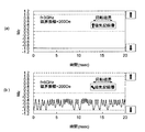
一般に、磁性体は異方性エネルギーや飽和磁化に応じて、マイクロ波磁界と共鳴する固有な共鳴周波数を有している。膜面に垂直な方向の磁化(以下、垂直磁化ともいう)を有する磁性体に対して膜面に平行な方向に、共鳴周波数に対応したマイクロ波磁界を作用させると共鳴現象が生じ、垂直磁化は急速に膜面に平行な方向に傾き、歳差運動を始める。なお、膜面とは磁性体の上面を意味する。飽和磁化Msが800emu/cc、異方性エネルギーKuが1.0×107erg/ccの磁気パラメータをもつとともに垂直磁化を有し、直径30nmの円板形状の磁気記録層を用意する。この磁気記録層の膜面に平行な方向に回転面を持ち、上方からみたときに反時計周り方向に回転するマイクロ波磁界を上記磁気記録層に印加した場合を考える。この場合における、磁気記録層の膜面に垂直方向の磁化成分をシミュレーション計算した結果を図1(a)、1(b)にそれぞれ示す。図1(a)、1(b)はそれぞれマイクロ波磁界の回転周波数(以下、単に周波数ともいう。)が3GHz、6GHzで、振幅が同じ200Oeである場合のシミュレーション計算結果である。図1(a)、1(b)のそれぞれにおいて、横軸は磁化を示し、縦軸は磁気記録層における膜面に垂直方向の磁化成分Mzを示す。図1(a)、1(b)において、Mzの値が1.0であることは磁気記録層の磁化の向きが上向きである場合を示し、Mzの値が−1.0であることは磁気記録層の磁化の向きが下向きである場合を示す。このシミュレーション計算においては、図1(a)に示すように、印加されるマイクロ波磁界の周波数が3GHzの場合は、磁気記録層の磁化の向きは、マイクロ波磁界が印加される前の初期状態と同じ下向きとなっており、ほとんど磁化の向きは変化しない。これに対して、印加されるマイクロ波磁界の周波数が6GHzの場合は、磁気記録層の磁化は、明確に共鳴状態となり、磁化が膜面に垂直な方向から平行な方向に傾いていることがわかる。 In general, a magnetic material has a specific resonance frequency that resonates with a microwave magnetic field in accordance with anisotropic energy and saturation magnetization. When a microwave magnetic field corresponding to the resonance frequency is applied to a magnetic material having magnetization in a direction perpendicular to the film surface (hereinafter also referred to as perpendicular magnetization) in a direction parallel to the film surface, a resonance phenomenon occurs and perpendicular magnetization occurs. Rapidly tilts in a direction parallel to the membrane surface and begins precession. The film surface means the upper surface of the magnetic material. A disk-shaped magnetic recording layer having a magnetic parameter of saturation magnetization Ms of 800 emu / cc, anisotropy energy Ku of 1.0 × 10 7 erg / cc, perpendicular magnetization, and a diameter of 30 nm is prepared. Consider a case where a microwave magnetic field having a rotating surface in a direction parallel to the film surface of the magnetic recording layer and rotating counterclockwise when viewed from above is applied to the magnetic recording layer. In this case, the results of the simulation calculation of the magnetization component perpendicular to the film surface of the magnetic recording layer are shown in FIGS. 1 (a) and 1 (b), respectively. FIGS. 1A and 1B show simulation calculation results when the rotation frequency of the microwave magnetic field (hereinafter also simply referred to as frequency) is 3 GHz and 6 GHz and the same amplitude is 200 Oe. In each of FIGS. 1A and 1B, the horizontal axis represents magnetization, and the vertical axis represents a magnetization component Mz perpendicular to the film surface in the magnetic recording layer. In FIGS. 1A and 1B, the value of Mz being 1.0 indicates that the magnetization direction of the magnetic recording layer is upward, and that the value of Mz is −1.0. The case where the magnetization direction of the magnetic recording layer is downward is shown. In this simulation calculation, as shown in FIG. 1A, when the frequency of the applied microwave magnetic field is 3 GHz, the magnetization direction of the magnetic recording layer is the initial state before the microwave magnetic field is applied. The direction of magnetization is almost unchanged. On the other hand, when the frequency of the applied microwave magnetic field is 6 GHz, the magnetization of the magnetic recording layer is clearly in a resonance state, and the magnetization is inclined in a direction parallel to a direction perpendicular to the film surface. Recognize.
次に、マイクロ波磁界の周波数を変化させて得られる、膜面に垂直な方向の磁化成分Mzの最小値に関する、マイクロ波磁界の周波数依存性を図2に示す。ここで、膜面に垂直な方向の磁化成分Mzの最小値とは、マイクロ波磁界を印加し、磁化を共鳴状態にし、磁化が最も傾いたときの、膜面に垂直な磁化成分Mzの絶対値を意味する。図1(a)、1(b)から、この磁気記録層については、6GHz近辺で共鳴現象が生じ、磁化が傾くことが分かる。ここで重要なのは、マイクロ波磁界により膜面に垂直な磁化成分Mzがゼロを横切れば、すなわち、正から負または負から正に変化すれば、磁化の反転を生じさせることができること意味する。 Next, FIG. 2 shows the frequency dependence of the microwave magnetic field regarding the minimum value of the magnetization component Mz in the direction perpendicular to the film surface, which is obtained by changing the frequency of the microwave magnetic field. Here, the minimum value of the magnetization component Mz in the direction perpendicular to the film surface is the absolute value of the magnetization component Mz perpendicular to the film surface when a microwave magnetic field is applied to bring the magnetization into a resonance state and the magnetization is most inclined. Mean value. 1 (a) and 1 (b), it can be seen that in this magnetic recording layer, a resonance phenomenon occurs in the vicinity of 6 GHz and the magnetization is inclined. What is important here is that if the magnetization component Mz perpendicular to the film surface crosses zero by the microwave magnetic field, that is, changes from positive to negative or negative to positive, magnetization reversal can be caused.
飽和磁化Msが500emu/cc、異方性エネルギーKuが2.0×106erg/ccの垂直磁化を有する磁気記録層を用意する。そして、この磁気記録層の膜面に平行な方向に回転面を持つマイクロ波磁界を印加した場合の、磁化の時間依存性のシミュレーション結果を図3に示す。このシミュレーションにおいては、マイクロ波磁界を印加する前の磁気記録層の磁化の向きは膜面に略垂直かつ下向きで、マイクロ波磁界は、磁気記録層を上からみたときに反時計方向に回転する回転磁界である。図3は、磁化を膜面に垂直な成分(垂直磁化成分)と、膜面に平行な成分(平行磁化成分)にベクトル分解をして示している。垂直磁化成分をグラフg1で示し、平行磁化成分をグラフg2で示す。マイクロ波磁界を印加すると、平行磁化成分が明確に歳差運動を開始し、時間と共に垂直磁化成分が傾き、1500psec程度で垂直磁化成分の符号が負から正に変化し、すなわち磁化の方向が下向きから上向きに変化し、磁化の反転が起こったことを示している。以上説明したように垂直磁化を有する磁気記録層に、磁気記録層の磁化に共鳴する周波数(共鳴周波数)をもつマイクロ波磁界を印加すれば磁化の反転を起こすことが示された。 A magnetic recording layer having a perpendicular magnetization with a saturation magnetization Ms of 500 emu / cc and an anisotropic energy Ku of 2.0 × 10 6 erg / cc is prepared. FIG. 3 shows a simulation result of the time dependence of magnetization when a microwave magnetic field having a rotation surface in a direction parallel to the film surface of the magnetic recording layer is applied. In this simulation, the magnetization direction of the magnetic recording layer before applying the microwave magnetic field is substantially perpendicular and downward to the film surface, and the microwave magnetic field rotates counterclockwise when the magnetic recording layer is viewed from above. It is a rotating magnetic field. FIG. 3 shows magnetization by vector decomposition into a component perpendicular to the film surface (perpendicular magnetization component) and a component parallel to the film surface (parallel magnetization component). It shows the vertical magnetization component in the graph g 1, shows the parallel magnetization component in the graph g 2. When a microwave magnetic field is applied, the parallel magnetization component clearly starts precession, the perpendicular magnetization component tilts with time, and the sign of the perpendicular magnetization component changes from negative to positive at about 1500 psec, that is, the magnetization direction is downward. It shows that the magnetization reversal occurred. As described above, it was shown that when a microwave magnetic field having a frequency (resonance frequency) resonating with the magnetization of the magnetic recording layer is applied to the magnetic recording layer having perpendicular magnetization, the magnetization is reversed.
さらに共鳴磁界書き込みにおいて重要な点は磁気記録層の磁化の反転方向と、マイクロ波磁界の回転方向とが1対1に対応することである。図3に示したシミュレーションと同一条件で、マイクロ波磁界の回転方向を時計回りにした場合の磁化の時間依存性をシミュレーション計算した結果を図4に示す。図4からわかるように、回転方向を逆にしただけで垂直磁化成分(グラフg1で示す。)は殆ど変化せず、平行磁化成分(グラフg2で示す。)が振動していることが明らかになった。以上をまとめると、磁気記録層に対して所定の回転周波数および所定の回転方向を有するマイクロ波磁界を印加すれば、所望の方向に磁気記録層の磁化を反転させることが可能である。 Further, in the resonant magnetic field writing, an important point is that the magnetization reversal direction of the magnetic recording layer and the rotation direction of the microwave magnetic field have a one-to-one correspondence. FIG. 4 shows the result of simulation calculation of the time dependence of magnetization when the rotation direction of the microwave magnetic field is clockwise under the same conditions as the simulation shown in FIG. As can be seen from FIG. 4, only by the direction of rotation reversed (shown graphically g 1.) Perpendicular magnetization component hardly changes, that (shown graphically g 2.) Parallel magnetization component is vibrating It was revealed. In summary, if a microwave magnetic field having a predetermined rotation frequency and a predetermined rotation direction is applied to the magnetic recording layer, the magnetization of the magnetic recording layer can be reversed in a desired direction.
以下に図面を参照して本発明の実施形態を説明する。 Embodiments of the present invention will be described below with reference to the drawings.
(第1実施形態)
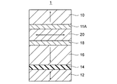
第1実施形態による磁気抵抗効果素子を図5に示す。本実施形態の磁気抵抗効果素子1は、磁化方向が可変の磁気記録層12と、トンネルバリア層14と、磁化方向が実質的に固定されている磁気参照層16と、スペーサ層18と、磁気回転層20とがこの順序で積層された積層構造、または逆の順序で積層された積層構造を備えている。
(First embodiment)
The magnetoresistive effect element according to the first embodiment is shown in FIG. The
磁気記録層12は磁化の方向が膜面に略垂直でかつ磁気抵抗効果素子1に電流が通電された場合に通電前後の磁化の向きを可変とすることが可能な強磁性層を有している。磁気参照層16は、磁化の方向が膜面に略垂直でかつ磁気抵抗効果素子1に電流が通電されても通電前後の磁化の向きは不変となる強磁性層を有している。なお、本実施形態においては、磁気参照層16の磁化の向きは、図5に示すように下向きとなっている。磁気回転層20は、磁化の方向が膜面に略平行でかつ磁気抵抗効果素子1に電流が通電された場合に磁化が略平行面内で磁化が回転する強磁性層を有している。
The
トンネルバリア層14は電子をトンネルさせ所望の磁気抵抗変化が得られる、例えばMg、Al、Ti、またはHfのいずれかの元素を含む酸化物もしくは窒化物からなっている。スペーサ層18はスピン偏極した電子を透過する非磁性層であって、その材料として、例えばCu、Au、Ru、またはAgのいずれかの元素のみからなる金属、もしくはこれらの元素を少なくとも1つ含む合金を用いることができる。また、例えばMg、Al、Ti、またはHfのいずれかの元素を含む酸化物もしくは窒化物を用いてもよい。
The
なお、本実施形態の磁気抵抗効果素子1においては、磁気記録層12の磁化方向で情報を記録するため、十分大きな垂直磁気異方性をもつ磁性体により形成し、熱擾乱に対する安定性を確保する必要がある。そのため、磁気記録層12として最適な磁性材料は、Fe、Co、Niのうちの少なくとも1つの元素と、Cr、Pt、Pd、Taのうちの少なくとも1つの元素とを含む規則合金もしくは不規則合金であることが望ましい。例えば、磁気記録層12は、Fe、Co、Niのうちの少なくとも1つの元素と、Pt、Pdのうち少なくとも1つの元素とを含むL10型結晶構造を有する磁性体で形成されることが好ましい。また、磁気記録層12は、Fe、Co、Niのうちの少なくとも1つの元素と、Cr、Pt、Pd、Taのうち少なくとも1つの元素とを含む六方晶型結晶構造を有する磁性体で形成されることが好ましい。また、磁気記録層12としては、希土類金属Sm、Gd、Tb、Dyのうち1つ以上の元素を含む、規則合金もしくは不規則合金で形成されても良い。
In the
本実施形態では、マイクロ波磁界の発生源として磁気回転層20を用いる。この磁気回転層20は、スピン偏極された電子が注入されると、磁気回転層20に注入されたスピン偏極した電子のスピンの向きに左ねじが進むとした場合に左ねじの回転する方向に磁気回転層20の磁化が回転する。本実施形態において、磁気記録層12からトンネルバリア層14、磁気参照層16、スペーサ層18を介して磁気回転層20に書き込み電流を流す場合、すなわち電子を磁気回転層20からスペーサ層18、磁気参照層16、トンネルバリア層14を介して磁気記録層12に流す場合を考える。この場合、磁気参照層16の磁化の向きが下向きとなっているので、磁気回転層20を通過した電子は、磁気参照層16によってスピン偏極され、磁気参照層16の磁化と同じ向きのスピンを有するスピン偏極された電子と、磁気参照層16の磁化と逆の向きのスピンを有するスピン偏極された電子に分離される。磁気参照層16の磁化と同じ向きのスピンを有するスピン偏極された電子は、磁気参照層16を通過する。しかし、磁気参照層16の磁化と逆の向きのスピンを有するスピン偏極された電子は、磁気参照層16によって反射され、スペーサ層18を介して磁気回転層20に注入され磁気回転層20の磁化が回転し始める。このときの回転方向は、磁気回転層20に注入されたスピン偏極した電子の向きは上向きであるので、磁気回転層20の磁化は磁気回転層20を上方からみたときに時計方向となる。
In the present embodiment, the
本実施形態において、上述の場合と逆方向に電流を流すと、すなわち電子を磁気記録層12、トンネルバリア層14、磁気参照層16、スペーサ層18を介して磁気回転層20に流すと、磁気回転層20に注入されるスピン偏極した電子は、磁気参照層16の磁化と同じ下向きのスピンを有する。このため、磁気回転層20の磁化は磁気回転層20を上方からみたときに反時計方向に回転する。
In the present embodiment, when a current is passed in the opposite direction to that described above, that is, when electrons are passed through the
磁気回転層20の磁化が回転することによって発生するマイクロ波磁界が磁気記録層12に印加される様子を図6に示す。磁気回転層20にスピン偏極した電子を注入した場合の回転周波数fiは、LLG(Landau-Lifshitz-Gilbert)方程式を解くことにより以下の式で表される(例えば、M. Mansuripur, J. Appl. Phys., 63:5809, 1988参照)。

本実施形態において、上式を用いて求めた、磁気回転層20に電流を流した際の回転周波数(歳差周波数)の電流密度依存性を図7に示す。ここで、回転周波数は磁気回転層20を上からみたときに時計方向に回転する場合を正とし反時計方向に回転する場合を負とし、電流密度Jは磁気記録層12からトンネルバリア層14、磁気参照層16、およびスペーサ層18を介して磁気回転層20に電流を流す方向を正とし逆方向に流す場合を負とする。図7からわかるように、電流密度J、磁気回転層20の磁気パラメータ(例えば、飽和磁化Msまたは偏極度P)を調節することで磁気回転層20の回転周波数を調節することができることが分かる。例えば、電流密度Jの絶対値を大きくすることで回転周波数の絶対値を上昇させることができ、また電流密度Jが一定ならば偏極度Pを大きくすることで回転周波数の絶対値を上昇させることができる。ここで重要なのは、所望の電流密度Jにおける磁気回転層20の回転周波数が磁気記録層12の共鳴周波数と一致すれば、先に述べたように共鳴磁界書き込みを行うことが可能となり、電流密度を変化させて回転周波数を磁気記録層12の共鳴周波数からずらせば共鳴磁界書き込みが起こらないことである。この性質を利用すれば、本発明の一実施形態の特徴である一方向の電流を用いて、情報“0”、“1”に対応した磁気記録層の磁化方向に反転させることが可能となる。
FIG. 7 shows the current density dependence of the rotation frequency (precession frequency) when a current is passed through the
磁気記録層の共鳴周波数の好適値は熱擾乱指数と共鳴周波数の依存性により求められる。磁気記録層の共鳴周波数は次のKittelの式で表される。
一方、熱擾乱指数は実効磁気異方性エネルギーKueffと、磁気抵抗効果素子の体積との積で表される。磁気メモリにおいては、磁気抵抗効果素子のばらつきを考慮して、熱による異常な反転が起こらないように熱擾乱指数を設定する必要があり、熱擾乱指数が30から120であることが好ましい。熱擾乱指数が30から120である場合の、共鳴磁界書き込みが起こるための、磁気記録層の好適な共鳴周波数の範囲は、2GHz〜40GHzである。 On the other hand, the thermal disturbance index is represented by the product of the effective magnetic anisotropy energy Kueff and the volume of the magnetoresistive element. In a magnetic memory, it is necessary to set a thermal disturbance index so that abnormal reversal due to heat does not occur in consideration of variations in magnetoresistive elements, and the thermal disturbance index is preferably 30 to 120. When the thermal disturbance index is 30 to 120, the preferable resonance frequency range of the magnetic recording layer for the resonance magnetic field writing to occur is 2 GHz to 40 GHz.
磁気回転層は、回転効率を高めるために、偏極率が大きい面内磁化膜が好ましく、Fe、Co、Niのうちの少なくとも1つの元素と、B、Si、Cのうちの少なくとも1つの元素とを含む磁性体を用いるか、もしくはFe、Co、Niのうちの少なくとも1つの元素を含む合金(例えば、CoFe、Fe、CoFeNi)などを用いることが好ましい。 The magnetic rotation layer is preferably an in-plane magnetization film having a large polarization rate in order to increase the rotation efficiency. At least one element of Fe, Co, and Ni and at least one element of B, Si, and C is preferable. It is preferable to use a magnetic body containing or an alloy containing at least one element of Fe, Co, Ni (for example, CoFe, Fe, CoFeNi).
磁気参照層は、安定したスピン注入を磁気記録層および磁気回転層に対して行うために、回転効率を高めるために、大きな垂直磁気異方性をもつことが望ましく、Fe、Co、Niのうちの少なくとも1つの元素と、Cr、Ta、Pt、Pdのうちの少なくとも1つの元素とを含む垂直磁気異方性を持つ磁性体を用いることが好ましい。また、Tb、Dy、Gd、Hoなどの希土類元素の少なくとも1つの元素と、Fe、Co、Niのうちの少なくとも1つの元素を含む垂直磁気異方性を持つ磁性体を用いても良い。また、磁気記憶層および磁気回転層に対して、偏極率が大きいことが必要であることから、上に挙げた磁気参照層の磁性体と、Fe、Co、Niのうちの少なくとも1つの元素およびB、Si、Cの少なくとも1つの元素を含む磁性体とを積層させた積層構造型の磁気参照層、もしくは上に挙げた磁気参照層の磁性体と、Fe、Co、Niのうちの少なくとも1つの元素を含む合金(例えば、CoFe、Fe、CoFeNi)とを積層させた積層構造型の磁気参照層を用いてもよい。 The magnetic reference layer preferably has a large perpendicular magnetic anisotropy in order to increase the rotation efficiency in order to perform stable spin injection to the magnetic recording layer and the magnetic rotation layer, and among Fe, Co and Ni It is preferable to use a magnetic material having perpendicular magnetic anisotropy including at least one element of the above and at least one element of Cr, Ta, Pt, and Pd. A magnetic material having perpendicular magnetic anisotropy including at least one element of rare earth elements such as Tb, Dy, Gd, and Ho and at least one element of Fe, Co, and Ni may be used. Further, since it is necessary for the magnetic storage layer and the magnetic rotation layer to have a high polarization rate, the magnetic material of the magnetic reference layer mentioned above and at least one element of Fe, Co, and Ni And a magnetic reference layer of a laminated structure type in which a magnetic material containing at least one element of B, Si, and C is laminated, or a magnetic material of the magnetic reference layer listed above, and at least of Fe, Co, and Ni A laminated structure type magnetic reference layer in which an alloy containing one element (for example, CoFe, Fe, CoFeNi) is laminated may be used.
本実施形態の磁気抵抗効果素子1は、磁気記録層12に磁化の反転を起こす2つの異なる書き込み機構をもつことに特徴がある。一つは、磁気記録層12からトンネルバリア層14、磁気参照層16、およびスペーサ層18を介して磁気回転層20に書き込み電流を流した時に、磁気参照層16からのスピン偏極した電子がトンネルバリア層14を介して磁気記録層12に注入されることによるスピン注入書き込みである。他の一つは磁気参照層16によって反射されたスピン偏極した電子がスペーサ層18を介して磁気回転層20に注入されることにより、磁気回転層20から発生するマイクロ波磁界の磁気記録層12への印加による共鳴磁界書き込みである。この共鳴磁界書き込みは、磁気記録層12に印加されるマイクロ波磁界の回転方向に左ねじが回転するとした場合に左ねじが進む方向と同じ方向の磁化に書き込まれる。スピン注入書き込みと共鳴磁界書き込みの反転方向が異なりかつそれぞれの書き込み機構における反転電流値が異なるように素子設計を行えば、異なる電流値の一方向の電流を流すことで情報“0”、“1”に対応した磁化方向に反転させることが可能となる。
The
特に、共鳴磁界書き込みについては、上述したように磁気回転層20の磁化、偏極度Pなどの磁気パラメータを変化させることにより、共鳴磁界書き込みに必要な電流値を自在に変化させることができ、磁化の回転方向については磁気参照層16の向きを逆にする、もしくは後述する第3実施形態に示すように、磁気回転層20として反強磁性結合膜(Synthetic Anti-Ferromagnetic Coupling)を用いることで、変えることが可能となる。
In particular, with respect to the resonant magnetic field writing, by changing the magnetic parameters such as the magnetization of the
本実施形態の磁気抵抗効果素子1における、磁気参照層16の磁化方向に対する磁気記録層12の磁化方向が平行状態から反平行状態への磁化反転する場合を図8(a)、8(b)を参照して説明する。図8(a)では、磁気記録層12および磁気参照層16の磁化方向は平行でかつ下向きとする。この状態で、回転周波数が磁気記録層12の共鳴周波数と等しい、もしくは共鳴周波数の近傍となるマイクロ磁界を磁気回転層20が発生する電流密度である第1書き込み電流を磁気記録層12からトンネルバリア層14、磁気参照層16、スペーサ層18を介して磁気回転層20に流す。この場合、第1書き込み電流は、磁気参照層16によってスピン偏極されて磁気参照層16の磁化と同じ向きのスピンを有する電子が磁気記録層12に作用することによるスピントランスファトルクを、共鳴磁界によって磁気記録層12に生じる反転トルクよりも小さくなるような電流値となっている。このため、第1書き込み電流を流しても、スピン注入書き込みは起こらず、共鳴磁界書き込みが生じる。これにより、共鳴磁界書き込みにより、磁気参照層16の磁化方向に対する磁気記録層12の磁化方向が平行状態から反平行状態に変化する(図8(b))。すなわち磁化の反転が起こる。
8A and 8B show the case where the magnetization direction of the
一方、本実施形態の磁気抵抗効果素子1における、磁気参照層16の磁化方向に対する磁気記録層12の磁化方向が反平行状態から平行状態への磁化反転する場合を図9(a)、9(b)を参照して説明する。図9(a)では、磁気記録層12および磁気参照層16の磁化方向は反平行でかつ磁気記録層12の磁化方向は上向きとする。この状態で第2書き込み電流を流す。この第2書き込み電流は、この電流によって磁気回転層20から発生されるマイクロ波磁界の回転周波数が磁気記録層12の共鳴周波数からずれるように選択される。このため、第2書き込み電流を流しても、共鳴磁界書き込みは起こらない。しかし、第2書き込み電流は、磁気参照層16によってスピン偏極され磁気参照層16の磁化と同じ向きのスピンを有するスピン偏極した電子が磁気記録層12に注入され、これによりスピン注入反転が生じる電流値となっている。このスピン注入反転により、磁気参照層16の磁化方向に対する磁気記録層12の磁化方向が反平行状態から平行状態へ変化する(図9(b))。すなわち磁化の反転が起こる。ここで、注意したいのは、磁気回転層20や磁気記録層12の磁気パラメータを変化させることで、マイクロ波磁界の周波数や共鳴周波数を変化させることが可能である。
On the other hand, in the
次に、本実施形態の磁気抵抗効果素子1をモデルとし、LLGシミュレーションによって計算した一方向電流を用いた書き込み結果を図10(a)、10(b)に示す。図10(a)は電流密度が2MA/cm2、図10(b)は電流密度が4MA/cm2のシミュレーション結果をそれぞれ示している。なお、図10(a)、10(b)のそれぞれの上下における矢印の組は磁気参照層16と磁気記録層12の磁化の向きを示す組である。各組において、上の矢印が磁気参照層16の磁化の向きを示し下の矢印が磁気記録層12の磁化の向きを示す。図10(a)、10(b)からわかるように、スピン注入書き込みにより電流密度2MA/cm2で反平行状態から平行状態への磁化反転が生じ、共鳴磁界書き込みにより電流密度4MA/cm2で平行状態から反平行状態への磁化反転が生じていることが明らかである。なお、図10(b)においては、書き込みの途中で共鳴磁界書き込みによる反転トルクと、スピン注入書き込みによる反転トルクが互いに逆に働いて、磁気記録層の磁化の向きが揺動するが、段々と共鳴磁界書き込みによる反転トルクの方が勝って共鳴磁界書き込みが行われる。本実施形態の磁気抵抗効果素子1において、一方向の電流の電流密度を変化させることで、情報“0”、“1”に対応した磁化方向に反転させることが可能であることが示された。したがって、パルス幅の精密な制御等が不要となり、誤書き込みのない安定な書き込みを行うことができる。
Next, FIGS. 10A and 10B show write results using the unidirectional current calculated by LLG simulation using the
なお、図10(a)、10(b)では一例として磁気参照層16の磁化方向を図面上で下向きとしたが、磁気参照層16の磁化方向を逆にして上向きとするとともに、磁気抵抗効果素子に流す電流の向きも逆にした場合でも同様の効果を得ることは可能である。
10A and 10B, as an example, the magnetization direction of the
図10(a)、10(b)では、スピン注入電流書込みに必要な電流が、共鳴磁界書込みと比べて小さい場合のシミュレーション結果を示したが、磁気回転層の磁気パラメータを変更することにより、共鳴磁界書込みに必要な電流を下げることは可能である。(1)式で示したように印加する電流密度に対する磁気回転層の回転周波数は、磁気回転層のジャイロ磁気定数γに比例し、ダンピング定数α、偏極率P、飽和磁化Ms、膜厚tに逆比例する。したがって、磁気回転層の磁気パラメータを最適化して、スピン注入書込みに必要な電流密度よりも小さい電流で磁気回転層の回転周波数が磁気記録層の共鳴周波数程度に達するようにすることで、共鳴磁界書込みに必要な電流をスピン注入書込みに必要な電流よりも下げることができる。 10 (a) and 10 (b) show simulation results when the current required for spin injection current writing is smaller than that for resonant magnetic field writing. By changing the magnetic parameters of the magnetic rotation layer, It is possible to reduce the current required for writing the resonant magnetic field. As shown in the equation (1), the rotation frequency of the magnetic rotating layer with respect to the applied current density is proportional to the gyromagnetic constant γ of the magnetic rotating layer, the damping constant α, the polarization rate P, the saturation magnetization M s , and the film thickness. Inversely proportional to t. Therefore, by optimizing the magnetic parameters of the magnetic rotation layer so that the rotation frequency of the magnetic rotation layer reaches about the resonance frequency of the magnetic recording layer with a current smaller than the current density required for spin injection writing, The current required for writing can be made lower than the current required for spin injection writing.
図11(a)、11(b)にLLGシミュレーションにより計算した、磁気回転層の磁気パラメータを最適化し共鳴磁界書込みの電流密度が小さい場合の、一方向電流を用いた書込み結果を示す。図11(a)、11(b)からわかるように、共鳴磁界書込みにより電流密度1.6MA/cm2で平行状態から反平行状態への磁化反転が生じ、スピン注入電流書き込みにより電流密度2.5MA/cm2で反平行状態から平行状態への磁化反転が生じていることが明らかであり、共鳴磁界書込みに必要な電流密度がスピン注入電流書込みの電流密度よりも小さい場合でも、本実施形態の磁気抵抗効果素子1において、一方向の電流の電流密度を変化させることで、情報“0”、“1”に対応した磁化方向に反転させることが可能であることが示された。スピン注入書込み電流密度よりも共鳴磁界書込みの電流密度が小さい場合のほうが、その反対の場合に比べて磁気抵抗効果素子の書き込み電流を小さくすることができる。
FIGS. 11 (a) and 11 (b) show the results of writing using a unidirectional current when the magnetic parameters of the magnetic rotating layer calculated by the LLG simulation are optimized and the current density of resonant magnetic field writing is small. As can be seen from FIGS. 11A and 11B, magnetization reversal from a parallel state to an antiparallel state occurs at a current density of 1.6 MA / cm 2 by resonant magnetic field writing, and current density of 2. It is clear that the magnetization reversal from the antiparallel state to the parallel state occurs at 5 MA / cm 2 , and even when the current density required for the resonant magnetic field writing is smaller than the current density of the spin injection current writing, the present embodiment In the
以上説明したように、本実施形態によれば、単一方向電流を用いて誤書き込みのない安定な書き込みを行うことの可能な磁気抵抗効果素子を提供することができる。 As described above, according to the present embodiment, it is possible to provide a magnetoresistive effect element capable of performing stable writing without erroneous writing using a unidirectional current.
(第2実施形態)
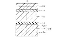
一般に、垂直磁化を有する磁性膜(垂直磁化膜)を用いた磁気抵抗効果素子では磁気記録層に磁気参照層からの漏れ磁界が作用し、情報“0”、“1”の安定性が非対称になる。このため、第2実施形態による磁気抵抗効果素子は、磁気参照層からの漏れ磁界の影響を低減するために、磁気参照層の磁化と逆方向の磁化をもつ磁界調整層を設けた構成となっている。この第2実施形態の磁気抵抗効果素子を図12に示す。この第2実施形態の磁気抵抗効果素子1は、図5に示す第1実施形態の磁気抵抗効果素子において、磁気記録層12の、トンネルバリア層14が設けられた側と反対側に非磁性金属層11を挟んで磁界調整層10を設けた構成となっている。非磁性金属層11の材料としては、Cu、Au、Ag、またはRuのいずれか元素のみからなる金属、またはこれらの元素の少なくとも1つを含む合金が用いられる。
(Second Embodiment)
In general, in a magnetoresistive effect element using a magnetic film having perpendicular magnetization (perpendicular magnetization film), a leakage magnetic field from the magnetic reference layer acts on the magnetic recording layer, and the stability of information “0” and “1” is asymmetric. Become. For this reason, the magnetoresistive effect element according to the second embodiment has a configuration in which a magnetic field adjustment layer having magnetization opposite to the magnetization of the magnetic reference layer is provided in order to reduce the influence of the leakage magnetic field from the magnetic reference layer. ing. The magnetoresistive effect element according to the second embodiment is shown in FIG. The
なお、図13に示す第2実施形態の変形例による磁気抵抗効果素子1のように、図5に示す第1実施形態において、磁気回転層20の、スペーサ層18が設けられた側と反対側に非磁性層11Aを挟んで磁界調整層10を設けた構成としてもよい。この変形例における非磁性層11Aとしては、スピン偏極電子を透過させない金属もしくはトンネル障壁層でも良い。しかし、この非磁性層11Aとしては、スピン偏極電子を透過する非磁性層、例えばCu、Au、Ag、またはRuのいずれかの元素のみからなる金属、これらの元素のうちの少なくとも1つを含む合金、もしくは例えばMg、Al、Ti、またはHfのいずれかの元素を含む酸化物もしくは窒化物からなっていることが好ましい。これらの材料を非磁性層11Aとして用いることにより、磁化回転層に対するスピン注入量が増加するために、効率的な磁化回転層の回転を起こすことが可能となるからである。
As in the
この第2実施形態およびその変形例も第1実施形態と同様に、単一方向電流を用いて誤書き込みのない安定な書き込みを行うことができる。また、第1実施形態に比べて、磁気参照層16からの漏れ磁界の影響を低減することが可能となり、磁気記録層12に記録された情報をより安定なものとすることができる。
Similarly to the first embodiment, the second embodiment and its modified example can perform stable writing without erroneous writing using a unidirectional current. Further, compared to the first embodiment, it is possible to reduce the influence of the leakage magnetic field from the
(第3実施形態)
第3実施形態の磁気抵抗効果素子を図14に示す。この第3実施形態の磁気抵抗効果素子1は、図5に示す第1実施形態の磁気抵抗効果素子において、磁気回転層20として反強磁性結合膜20Aを用いた構成となっている。この反強磁性結合膜20Aは、スペーサ層18上、強磁性層20a、非磁性層20b、および強磁性層20cが、この順序で積層された積層構造を有し、強磁性層20aと強磁性層20cは、非磁性層20bを介して反強磁性結合をしている。
(Third embodiment)
The magnetoresistive effect element of 3rd Embodiment is shown in FIG. The
第1乃至第2実施形態による磁気抵抗効果素子においては、磁気回転層20として面内磁化を有する磁性膜(面内磁化膜)を用いるため、ボルテックス磁区構造などの複雑な磁区構造が生じる場合がある。磁区構造があると磁気参照層16からのスピン注入が行われた際の回転が互いに阻害され、回転効率が落ちるため、磁気回転層20には磁区構造が生じないことが望ましい。一般的に素子サイズを小さくすることにより面内磁化膜は単磁区化して磁区構造が生じない性質がある。さらに、面内磁化膜である磁気回転層において磁区構造を生じさせなくするためには、第3実施形態のように、磁気回転層20Aとして反強磁性結合膜を用いればよい。
In the magnetoresistive effect element according to the first or second embodiment, since a magnetic film having in-plane magnetization (in-plane magnetization film) is used as the
したがって、第3実施形態の磁気抵抗効果素子1は、磁気回転層20Aの回転効率が低下するのを防止することができる。また、第3実施形態の磁気抵抗効果素子1も、第1実施形態と同様に、単一方向電流を用いて誤書き込みのない安定な書き込みを行うことができる。
Therefore, the
なお、第3実施形態において、反強磁性結合膜20Aの強磁性層20a、20cの膜厚に差をつけることで、磁気回転層20Aから磁気記録層12へ印加されるマイクロ波磁界の回転方向を、単一膜で形成された磁気回転層の場合と逆にすることも可能である。
In the third embodiment, the rotation direction of the microwave magnetic field applied from the magnetic rotation layer 20A to the
(第4実施形態)
第4実施形態による磁気抵抗効果素子を図15に示す。第4実施形態の磁気抵抗効果素子1は、図5に示す第1実施形態の磁気抵抗効果素子において、磁気記録層12として、垂直磁化膜12aに面内磁化膜12bを積層して積層型の磁気記録層12Aを用いた構成となっている。
(Fourth embodiment)
FIG. 15 shows a magnetoresistive effect element according to the fourth embodiment. The
第1乃至第3実施形態の磁気抵抗効果素子においては、磁気記録層の共鳴周波数が、共鳴磁界書き込みに重要なパラメータとなる。磁気記録層の共鳴周波数はKittelの式、すなわち(5)式で表されるように、磁気異方性エネルギーに依存する。したがって、第4実施形態のように磁気記録層として積層型の磁気記録層12Aを用いることで共鳴周波数を自由に変化させることができる。このとき面内磁化膜12bは垂直磁気異方性を持たないが、垂直磁化膜12aと交換結合することで、磁化方向は図15に示すように垂直方向を向く。一般的に、垂直磁化膜に面内磁化膜を積層すると全体の磁気異方性エネルギーは低下する。このため、第4実施形態の磁気記録層12Aの共鳴周波数が所望の周波数となるようにすることができる。なお、垂直磁化膜12aとしては、Fe、Co、Niのうちの少なくとも1つの元素と、Pt、Pdのうちの少なくとも1つの元素と、を含むL10型結晶構造をもつ磁性体を用いるか、または、Fe、Co、Niのうちの少なくとも1つの元素と、Cr、Ta、Pt、Pdのうちの少なくとも1つの元素とを含む六方晶型結晶構造を有する磁性体を用いることが好ましい。これらの場合、面内磁化膜12bとして、Fe、Co、Ni、Mnのうち少なくとも1つの元素を含む合金を用いることができる。
In the magnetoresistive effect element according to the first to third embodiments, the resonance frequency of the magnetic recording layer is an important parameter for writing the resonance magnetic field. The resonance frequency of the magnetic recording layer depends on the magnetic anisotropy energy as expressed by the Kittel equation, that is, the equation (5). Therefore, the resonance frequency can be freely changed by using the laminated
また、図16に示す変形例の磁気抵抗効果素子1のように垂直磁化膜12aと垂直磁化膜12dとの間にCu、Au、Ag、またはRuのいずれかの元素を含むスペーサ層12cを設けて反強磁性結合させた垂直型SAF結合膜12Bを用いても同様に、第1乃至第3実施形態に比べて共鳴周波数を変化させた磁気記録層12Bを作製することが可能である。
Further, a
この第4実施形態およびその変形例も、第1実施形態と同様に、単一方向電流を用いて誤書き込みのない安定な書き込みを行うことができる。 In the fourth embodiment and its modification, similarly to the first embodiment, stable writing without erroneous writing can be performed using a unidirectional current.
なお、第2乃至第4実施形態を適宜組み合わせても、第1実施形態と同様に、単一方向電流を用いて誤書き込みのない安定な書き込みを行うことができる。 Even if the second to fourth embodiments are appropriately combined, stable writing without erroneous writing can be performed using a unidirectional current, as in the first embodiment.
(第5実施形態)
次に、第5実施形態による磁気ランダムアクセスメモリ(MRAM)を図17に示す。本実施形態のMRAMは、マトリクス状に配列されたメモリセルMCを有するメモリセルアレイ100を備えている。そして、各メモリセルMCは、第1乃至第4実施形態およびその変形例のいずれかもしくは、それぞれ組み合わせた磁気抵抗効果素子1を備えている。
(Fifth embodiment)
Next, FIG. 17 shows a magnetic random access memory (MRAM) according to the fifth embodiment. The MRAM of this embodiment includes a
また、メモリセルアレイ100には、それぞれが列(カラム)方向に延在するように、複数のビット線対BL、/BLが配置されている。また、メモリセルアレイ100には、それぞれが行(ロウ)方向に延在するように、複数のワード線WLが配置されている。
In the
ビット線BLとワード線WLとの交差部分には、メモリセルMCが配置されている。各メモリセルMCは、磁気抵抗効果素子1と選択トランジスタ40とを有している。磁気抵抗効果素子1の一端は、ビット線BLに接続されている。磁気抵抗効果素子1の他端は、選択トランジスタ40のドレイン端子に接続されている。選択トランジスタ40のゲート端子は、ワード線WLに接続されている。選択トランジスタ40のソース端子は、ビット線/BLに接続されている。
Memory cells MC are arranged at the intersections between the bit lines BL and the word lines WL. Each memory cell MC has a
ワード線WLには、ロウデコーダ50が接続されている。ビット線対BL、/BLには、書き込み回路および読み出し回路60が接続されている。書き込み回路および読み出し回路60には、カラムデコーダ70が接続されている。各メモリセルMCは、ロウデコーダ50およびカラムデコーダ70により選択される。
A
メモリセルMCへのデータ書き込みは、以下のように行われる。先ず、データ書き込みを行なうメモリセルMCを選択するために、このメモリセルMCに接続されたワード線WLが活性化される。これにより、選択トランジスタ40がオンする。
Data writing to the memory cell MC is performed as follows. First, in order to select a memory cell MC for data writing, the word line WL connected to the memory cell MC is activated. Thereby, the
ここで、磁気抵抗効果素子1には、一方向のみの書き込み電流が供給されればよい。具体的には、磁気抵抗効果素子1に図面上で左から右へ書き込み電流Iwを供給する場合、書き込み回路および読み出し回路60中の書き込み回路は、ビット線BLに正の電位を印加し、ビット線/BLに接地電位を印加する。このようにして、メモリセルMCにデータ“0”或いはデータ“1”を書き込むことができる。
Here, the
メモリセルMCからのデータ読み出しは、以下のように行われる。先ず、メモリセルMCが選択される。書き込み回路および読み出し回路60中の読み出し回路は、磁気抵抗効果素子1に、例えば図面上で右から左へ流れる読み出し電流Irを供給する。そして、上記読み出し回路は、この読み出し電流Irに基づいて、磁気抵抗効果素子1の抵抗値を検出する。このようにして、磁気抵抗効果素子1に記憶された情報を読み出すことができる。この第5実施形態のMRAMでは、双方向に書き込み電流を流すための周辺回路を搭載する必要がなくなるためセル占有率が高い大容量のMRAMを実現することが容易となる。
Data reading from the memory cell MC is performed as follows. First, the memory cell MC is selected. The read circuit in the write circuit and the
(第6実施形態)
第6実施形態によるMRAMを図18に示す。第6実施形態のMRAMは、クロスポイント型のアーキテクチャを有している。すなわち、第6実施形態のMRAMは、ビット線BLとワード線WLとの間に、第1乃至第4実施形態のいずれかの磁気抵抗効果素子1と、ダイオード80とを含むメモリセルMCを備えた構成となっている。なお、ダイオード80としては、PNダイオードやショットキーダイオードを用いることができる。また、ダイオード80の代わりに一方向にのみ電流を流す整流機能を有している整流素子を用いてもよい。なお、図18においては、ビット線側にダイオード80を設けたがワード線WL側に設けてもよい。
(Sixth embodiment)
An MRAM according to the sixth embodiment is shown in FIG. The MRAM of the sixth embodiment has a cross-point type architecture. That is, the MRAM of the sixth embodiment includes a memory cell MC including the
第6実施形態においては、一方向にしか電流を流すことができないので、書き込みには、第1実施形態で説明した第1および第2書き込み電流を用い、読み出し電流としては、磁気記録層12の共鳴周波数からずれた回転周波数を有するマイクロ波磁界を磁気回転層20が発生する電流値であってかつ磁気記録層12の磁化方向がスピン注入により反転しない電流値を用いることが好ましい。
In the sixth embodiment, since current can flow only in one direction, the first and second write currents described in the first embodiment are used for writing, and the read current of the
この場合は、ロウデコーダおよびカラムデコーダの組み合わせにより、書き込みおよびお読み出しを行うメモリセルを選択することが可能である。この第6実施形態のMRAMでは、各メモリセルに選択トランジスタを搭載する必要がなくなるため、セル占有率が高い大容量のMRAMを実現することが可能となる。 In this case, it is possible to select a memory cell for writing and reading by a combination of a row decoder and a column decoder. In the MRAM according to the sixth embodiment, since it is not necessary to mount a selection transistor in each memory cell, it is possible to realize a large-capacity MRAM with a high cell occupation rate.
なお、第6実施形態のMRAMは、図18に示すように下層と上層にそれぞれクロスポイント型アーキテクチャを備えた構成とし、下層および上層のクロスポイント型アーキテクチャにおける同一位置に対応する配線、例えばビット線BLを共有するように配置すれば、積層型のMRAMを形成することが可能である。また図18に示す回路構成を単位階層とすれば、原理上、N回積層して、単位面積あたりの容量をN倍させた超大容量メモリを形成することが可能である。 As shown in FIG. 18, the MRAM of the sixth embodiment has a configuration in which a lower layer and an upper layer are each provided with a cross-point type architecture, and wirings corresponding to the same positions in the lower layer and the upper layer cross-point type architecture, for example, bit lines If the BLs are arranged so as to share the same, a stacked MRAM can be formed. Further, if the circuit configuration shown in FIG. 18 is a unit hierarchy, in principle, it is possible to form a very large capacity memory that is stacked N times and the capacity per unit area is increased N times.
本発明のいくつかの実施形態を説明したが、これらの実施形態は、例として提示したものであり、発明の範囲を限定することは意図していない。これらの実施形態は、その他の様々な形態で実施されることが可能であり、発明の要旨を逸脱しない範囲で、種々の省略、置き換え、変更を行うことができる。これらの実施形態やその変形は、発明の範囲や要旨に含まれると同様に、特許請求の範囲に記載された発明とその均等の範囲に含まれるものである。 Although several embodiments of the present invention have been described, these embodiments are presented by way of example and are not intended to limit the scope of the invention. These embodiments can be implemented in various other forms, and various omissions, replacements, and changes can be made without departing from the scope of the invention. These embodiments and modifications thereof are included in the invention described in the claims and equivalents thereof as well as included in the scope and gist of the invention.
本発明のいくつかの実施形態を説明したが、これらの実施形態は、例として提示したものであり、発明の範囲を限定することは意図していない。これらの実施形態は、その他の様々な形態で実施されることが可能であり、発明の要旨を逸脱しない範囲で、種々の省略、置き換え、変更を行うことができる。これらの実施形態やその変形は、発明の範囲や要旨に含まれると同様に、特許請求の範囲に記載された発明とその均等の範囲に含まれるものである。 Although several embodiments of the present invention have been described, these embodiments are presented by way of example and are not intended to limit the scope of the invention. These embodiments can be implemented in various other forms, and various omissions, replacements, and changes can be made without departing from the scope of the invention. These embodiments and modifications thereof are included in the invention described in the claims and equivalents thereof as well as included in the scope and gist of the invention.
1 磁気抵抗効果素子
10 磁界調整層
11 非磁性金属層
12 磁気記録層
12A 磁気記録層
12B 磁気記録層
12a 垂直磁化膜
12b 面内磁化膜
12c 非磁性層
14 トンネルバリア層
16 磁気参照層
18 スペーサ層
20 磁気回転層
20A 磁気回転層
20a 強磁性層
20b 非磁性層
20c 強磁性層
40 選択トランジスタ
50 ロウデコーダ
60 書き込み回路/読み出し回路
70 カラムデコーダ
80 ダイオード
100 メモリセルアレイ
DESCRIPTION OF
Claims (12)
磁化が膜面に対して略垂直でかつ不変の第2強磁性層と、
前記第1強磁性層と前記第2強磁性層との間に設けられる第1非磁性層と、
前記第2強磁性層に対して前記第1非磁性層と反対側に設けられ、膜面に略平行な磁化を有し、スピン偏極された電子が注入されることによりマイクロ波磁界を発生する第3強磁性層と、
前記第2強磁性層と前記第3強磁性層との間に設けられる第2非磁性層と、
を備え、
前記第3強磁性層から前記第2強磁性層を介して前記第1強磁性層に向かう方向および前記第1強磁性層から前記第2強磁性層を介して前記第3強磁性層に向かう方向のうちの一方の方向に第1電流を流すことにより前記第3強磁性層から発生する前記マイクロ波磁界によって前記第1強磁性層の磁化が反転可能であり、
前記一方の方向に前記第1電流と異なる電流密度を有する第2電流を流し前記第2強磁性層によってスピン偏極された電子によって前記第1強磁性層の磁化が、前記第1電流を流した場合と異なる方向に反転可能であることを特徴とする磁気抵抗効果素子。A first ferromagnetic layer whose magnetization is substantially perpendicular to the film surface and variable;
A second ferromagnetic layer whose magnetization is substantially perpendicular to the film surface and unchanged,
A first nonmagnetic layer provided between the first ferromagnetic layer and the second ferromagnetic layer;
Provided on the opposite side to the first nonmagnetic layer with respect to the second ferromagnetic layer, has a magnetization substantially parallel to the film surface, and generates a microwave magnetic field by injecting spin-polarized electrons A third ferromagnetic layer,
A second nonmagnetic layer provided between the second ferromagnetic layer and the third ferromagnetic layer;
With
The direction from the third ferromagnetic layer to the first ferromagnetic layer via the second ferromagnetic layer and the direction from the first ferromagnetic layer to the third ferromagnetic layer via the second ferromagnetic layer The magnetization of the first ferromagnetic layer can be reversed by the microwave magnetic field generated from the third ferromagnetic layer by flowing a first current in one of the directions;
A second current having a current density different from that of the first current flows in the one direction, and magnetization of the first ferromagnetic layer is caused to flow by the electrons spin-polarized by the second ferromagnetic layer. A magnetoresistive effect element which can be reversed in a direction different from that of the case.
Fe、Co、Niのうちの少なくとも1つの元素と、Pt、Pdのうちの少なくとも1つの元素と、を含むL10型結晶構造を有する磁性体か、または
Fe、Co、Niのうちの少なくとも1つの元素と、Cr、Ta、Pt、Pdのうちの少なくとも1つの元素とを含む六方晶型結晶構造を有する磁性体
のいずれかを備えることを特徴とする請求項1乃至5のいずれかに記載の磁気抵抗効果素子。 The first ferromagnetic layer includes
Fe, Co, and at least one element of Ni, Pt, magnetic or having an L1 0 type crystal structure containing at least one element, the one of Pd, or Fe, Co, of Ni at least 1 6. A magnetic material having a hexagonal crystal structure including one element and at least one element selected from Cr, Ta, Pt, and Pd is provided. Magnetoresistive effect element.
Fe、Co、Niのうちの少なくとも1つの元素と、Pt、Pdのうちの少なくとも1つの元素と、を含むL10型結晶構造を有する磁性体と、
Fe、Co、Ni、Mnのうち少なくとも1つの元素を含む合金と
を含む積層構造を備えることを特徴とする請求項1乃至5のいずれかに記載の磁気抵抗効果素子。 The first ferromagnetic layer includes
Fe, Co, and a magnetic body having at least one element of Ni, Pt, and at least one element of Pd, the L1 0 type crystal structure containing,
6. The magnetoresistive effect element according to claim 1, further comprising a laminated structure including an alloy containing at least one element of Fe, Co, Ni, and Mn.
Fe、Co、Ni、Mnのうち少なくとも1つの元素を含む合金と
を含む積層構造を備えることを特徴とする請求項1乃至5のいずれかに記載の磁気抵抗効果素子。 The first ferromagnetic layer includes a magnetic material having a hexagonal crystal structure including at least one element of Fe, Co, and Ni and at least one element of Cr, Ta, Pt, and Pd;
6. The magnetoresistive effect element according to claim 1, further comprising a laminated structure including an alloy containing at least one element of Fe, Co, Ni, and Mn.
前記磁気抵抗効果素子の前記第1強磁性層に第1電極を介して電気的に接続される第1配線と、
前記磁気抵抗効果素子の前記第3強磁性層に第2電極を介して電気的に接続される第2配線と、
を備えていることを特徴とする磁気ランダムアクセスメモリ。 The magnetoresistive effect element according to any one of claims 1 to 9,
A first wiring electrically connected to the first ferromagnetic layer of the magnetoresistive effect element via a first electrode;
A second wiring electrically connected to the third ferromagnetic layer of the magnetoresistive effect element via a second electrode;
A magnetic random access memory comprising:
Priority Applications (4)
| Application Number | Priority Date | Filing Date | Title |
|---|---|---|---|
| JP2010210181A JP5514059B2 (en) | 2010-09-17 | 2010-09-17 | Magnetoresistive element and magnetic random access memory |
| PCT/JP2011/071254 WO2012036282A1 (en) | 2010-09-17 | 2011-09-16 | Magnetoresistive element and magnetic random-access memory |
| CN201180039960.3A CN103069564B (en) | 2010-09-17 | 2011-09-16 | Magnetoresistive element and magnetic random-access memory |
| US13/781,529 US20130181305A1 (en) | 2010-09-17 | 2013-02-28 | Magnetoresistive element and magnetic random access memory |
Applications Claiming Priority (1)
| Application Number | Priority Date | Filing Date | Title |
|---|---|---|---|
| JP2010210181A JP5514059B2 (en) | 2010-09-17 | 2010-09-17 | Magnetoresistive element and magnetic random access memory |
Publications (2)
| Publication Number | Publication Date |
|---|---|
| JP2012064904A JP2012064904A (en) | 2012-03-29 |
| JP5514059B2 true JP5514059B2 (en) | 2014-06-04 |
Family
ID=45831735
Family Applications (1)
| Application Number | Title | Priority Date | Filing Date |
|---|---|---|---|
| JP2010210181A Expired - Fee Related JP5514059B2 (en) | 2010-09-17 | 2010-09-17 | Magnetoresistive element and magnetic random access memory |
Country Status (4)
| Country | Link |
|---|---|
| US (1) | US20130181305A1 (en) |
| JP (1) | JP5514059B2 (en) |
| CN (1) | CN103069564B (en) |
| WO (1) | WO2012036282A1 (en) |
Families Citing this family (46)
| Publication number | Priority date | Publication date | Assignee | Title |
|---|---|---|---|---|
| JP5214691B2 (en) * | 2010-09-17 | 2013-06-19 | 株式会社東芝 | Magnetic memory and manufacturing method thereof |
| KR101195041B1 (en) | 2011-05-12 | 2012-10-31 | 고려대학교 산학협력단 | Spin-transfer-torque magnetic random access memory using current-induced self-resonant switching |
| JP5535161B2 (en) | 2011-09-20 | 2014-07-02 | 株式会社東芝 | Magnetoresistive element and manufacturing method thereof |
| KR101375871B1 (en) * | 2012-04-09 | 2014-03-17 | 삼성전자주식회사 | Spin-transfer-torque magnetic random access memory using resonant and dual-spin-filter effects |
| US9231191B2 (en) * | 2012-08-20 | 2016-01-05 | Industrial Technology Research Institute | Magnetic tunnel junction device and method of making same |
| JP5383882B1 (en) * | 2012-09-26 | 2014-01-08 | 株式会社東芝 | Nonvolatile memory device |
| JP6160903B2 (en) * | 2013-03-13 | 2017-07-12 | 株式会社東芝 | Magnetic storage element and nonvolatile storage device |
| US9123879B2 (en) | 2013-09-09 | 2015-09-01 | Masahiko Nakayama | Magnetoresistive element and method of manufacturing the same |
| US9368717B2 (en) | 2013-09-10 | 2016-06-14 | Kabushiki Kaisha Toshiba | Magnetoresistive element and method for manufacturing the same |
| US9240547B2 (en) | 2013-09-10 | 2016-01-19 | Micron Technology, Inc. | Magnetic tunnel junctions and methods of forming magnetic tunnel junctions |
| US9385304B2 (en) | 2013-09-10 | 2016-07-05 | Kabushiki Kaisha Toshiba | Magnetic memory and method of manufacturing the same |
| US9231196B2 (en) | 2013-09-10 | 2016-01-05 | Kuniaki SUGIURA | Magnetoresistive element and method of manufacturing the same |
| JP6106118B2 (en) | 2014-03-13 | 2017-03-29 | 株式会社東芝 | Magnetic storage element and nonvolatile storage device |
| WO2015136748A1 (en) * | 2014-03-13 | 2015-09-17 | Sakai Shintaro | Variable change memory and the writing method of the same |
| JP6018599B2 (en) | 2014-03-20 | 2016-11-02 | 株式会社東芝 | Nonvolatile storage device |
| US9373779B1 (en) | 2014-12-08 | 2016-06-21 | Micron Technology, Inc. | Magnetic tunnel junctions |
| US9466350B2 (en) * | 2015-03-09 | 2016-10-11 | Kabushiki Kaisha Toshiba | Magnetic memory device |
| US9502642B2 (en) | 2015-04-10 | 2016-11-22 | Micron Technology, Inc. | Magnetic tunnel junctions, methods used while forming magnetic tunnel junctions, and methods of forming magnetic tunnel junctions |
| US9520553B2 (en) | 2015-04-15 | 2016-12-13 | Micron Technology, Inc. | Methods of forming a magnetic electrode of a magnetic tunnel junction and methods of forming a magnetic tunnel junction |
| US9530959B2 (en) | 2015-04-15 | 2016-12-27 | Micron Technology, Inc. | Magnetic tunnel junctions |
| US10468590B2 (en) | 2015-04-21 | 2019-11-05 | Spin Memory, Inc. | High annealing temperature perpendicular magnetic anisotropy structure for magnetic random access memory |
| US9728712B2 (en) | 2015-04-21 | 2017-08-08 | Spin Transfer Technologies, Inc. | Spin transfer torque structure for MRAM devices having a spin current injection capping layer |
| US9257136B1 (en) | 2015-05-05 | 2016-02-09 | Micron Technology, Inc. | Magnetic tunnel junctions |
| US9960346B2 (en) | 2015-05-07 | 2018-05-01 | Micron Technology, Inc. | Magnetic tunnel junctions |
| CN104947057B (en) * | 2015-06-04 | 2017-08-08 | 山西师范大学 | L10FePt Quito tunic wide field linear magnetoresistance sensor and preparation method thereof |
| US9853206B2 (en) | 2015-06-16 | 2017-12-26 | Spin Transfer Technologies, Inc. | Precessional spin current structure for MRAM |
| US9773974B2 (en) | 2015-07-30 | 2017-09-26 | Spin Transfer Technologies, Inc. | Polishing stop layer(s) for processing arrays of semiconductor elements |
| JP6130886B2 (en) | 2015-09-16 | 2017-05-17 | 株式会社東芝 | Magnetic element and storage device |
| US9741926B1 (en) | 2016-01-28 | 2017-08-22 | Spin Transfer Technologies, Inc. | Memory cell having magnetic tunnel junction and thermal stability enhancement layer |
| US9680089B1 (en) | 2016-05-13 | 2017-06-13 | Micron Technology, Inc. | Magnetic tunnel junctions |
| TWI684979B (en) * | 2016-09-09 | 2020-02-11 | 東芝記憶體股份有限公司 | Memory device |
| US10319901B2 (en) * | 2016-10-27 | 2019-06-11 | Tdk Corporation | Spin-orbit torque type magnetization reversal element, magnetic memory, and high frequency magnetic device |
| CN113659071B (en) * | 2017-02-27 | 2024-04-09 | Tdk株式会社 | Spin-current magnetization rotating element, magnetoresistance effect element, and magnetic memory |
| US10665777B2 (en) | 2017-02-28 | 2020-05-26 | Spin Memory, Inc. | Precessional spin current structure with non-magnetic insertion layer for MRAM |
| US10672976B2 (en) | 2017-02-28 | 2020-06-02 | Spin Memory, Inc. | Precessional spin current structure with high in-plane magnetization for MRAM |
| JP2019054054A (en) * | 2017-09-13 | 2019-04-04 | 東芝メモリ株式会社 | Magnetic device |
| US11637234B2 (en) | 2017-09-15 | 2023-04-25 | Tokyo Institute Of Technology | Manufacturing method for multilayer structure of magnetic body and BiSb layer, magnetoresistive memory, and pure spin injection source |
| JP6428988B1 (en) * | 2018-02-28 | 2018-11-28 | Tdk株式会社 | Spin element stabilization method and spin element manufacturing method |
| JP2020043134A (en) * | 2018-09-06 | 2020-03-19 | キオクシア株式会社 | Magnetic storage device |
| US11283010B2 (en) * | 2018-09-07 | 2022-03-22 | Integrated Silicon Solution, (Cayman) Inc. | Precessional spin current structure for magnetic random access memory with novel capping materials |
| JP6620913B1 (en) * | 2018-09-12 | 2019-12-18 | Tdk株式会社 | Reservoir element and neuromorphic element |
| US10580827B1 (en) | 2018-11-16 | 2020-03-03 | Spin Memory, Inc. | Adjustable stabilizer/polarizer method for MRAM with enhanced stability and efficient switching |
| US10797227B2 (en) | 2018-12-06 | 2020-10-06 | Sandisk Technologies Llc | Spin-transfer torque MRAM with a negative magnetic anisotropy assist layer and methods of operating the same |
| US10811596B2 (en) | 2018-12-06 | 2020-10-20 | Sandisk Technologies Llc | Spin transfer torque MRAM with a spin torque oscillator stack and methods of making the same |
| US10862022B2 (en) | 2018-12-06 | 2020-12-08 | Sandisk Technologies Llc | Spin-transfer torque MRAM with magnetically coupled assist layers and methods of operating the same |
| CN112420709B (en) * | 2019-08-23 | 2023-06-06 | 中国科学院物理研究所 | Conversion of PbTiO 3 /SrTiO 3 Method for vortex domain of superlattice material |
Family Cites Families (10)
| Publication number | Priority date | Publication date | Assignee | Title |
|---|---|---|---|---|
| FR2817998B1 (en) * | 2000-12-07 | 2003-01-10 | Commissariat Energie Atomique | SPIN POLARIZATION MAGNETIC DEVICE WITH MAGNIFICATION ROTATION, MEMORY AND WRITING METHOD USING THE DEVICE |
| TWI222630B (en) * | 2001-04-24 | 2004-10-21 | Matsushita Electric Ind Co Ltd | Magnetoresistive element and magnetoresistive memory device using the same |
| JP2008028362A (en) * | 2006-06-22 | 2008-02-07 | Toshiba Corp | Magnetoresistive element and magnetic memory |
| JP4874884B2 (en) * | 2007-07-11 | 2012-02-15 | 株式会社東芝 | Magnetic recording element and magnetic recording apparatus |
| JP2009081315A (en) * | 2007-09-26 | 2009-04-16 | Toshiba Corp | Magnetoresistive element, and magnetic memory |
| JP5260040B2 (en) * | 2007-12-19 | 2013-08-14 | 株式会社日立製作所 | Unidirectional current magnetization reversal magnetoresistive element and magnetic recording apparatus |
| JP4724196B2 (en) * | 2008-03-25 | 2011-07-13 | 株式会社東芝 | Magnetoresistive element and magnetic random access memory |
| JP4960319B2 (en) * | 2008-07-31 | 2012-06-27 | 株式会社東芝 | Magnetic recording device |
| WO2011096312A1 (en) * | 2010-02-04 | 2011-08-11 | 株式会社日立製作所 | Tunnel magnetoresistance effect element, and magnetic memory cell and magnetic random access memory employing same |
| JP5085703B2 (en) * | 2010-09-17 | 2012-11-28 | 株式会社東芝 | Magnetic recording element and nonvolatile memory device |
-
2010
- 2010-09-17 JP JP2010210181A patent/JP5514059B2/en not_active Expired - Fee Related
-
2011
- 2011-09-16 CN CN201180039960.3A patent/CN103069564B/en active Active
- 2011-09-16 WO PCT/JP2011/071254 patent/WO2012036282A1/en active Application Filing
-
2013
- 2013-02-28 US US13/781,529 patent/US20130181305A1/en not_active Abandoned
Also Published As
| Publication number | Publication date |
|---|---|
| CN103069564B (en) | 2015-06-17 |
| CN103069564A (en) | 2013-04-24 |
| JP2012064904A (en) | 2012-03-29 |
| WO2012036282A1 (en) | 2012-03-22 |
| US20130181305A1 (en) | 2013-07-18 |
Similar Documents
| Publication | Publication Date | Title |
|---|---|---|
| JP5514059B2 (en) | Magnetoresistive element and magnetic random access memory | |
| US7486552B2 (en) | Method and system for providing a spin transfer device with improved switching characteristics | |
| JP4724196B2 (en) | Magnetoresistive element and magnetic random access memory | |
| JP6717735B2 (en) | Spin-orbit torque bit design for improved switching efficiency | |
| US10460786B2 (en) | Systems and methods for reducing write error rate in magnetoelectric random access memory through pulse sharpening and reverse pulse schemes | |
| JP4250644B2 (en) | MAGNETIC STORAGE ELEMENT, MAGNETIC MEMORY HAVING THE MAGNETIC STORAGE ELEMENT, AND METHOD FOR DRIVING MAGNETIC MEMORY | |
| JP6244617B2 (en) | Storage element, storage device, magnetic head | |
| JP4915626B2 (en) | Magnetoresistive element and magnetic random access memory | |
| JP5062538B2 (en) | Magnetic memory element, driving method thereof, and nonvolatile memory device | |
| JP5987613B2 (en) | Storage element, storage device, magnetic head | |
| WO2012004883A1 (en) | Magnetoresistive effect element and random access memory using same | |
| WO2013080436A1 (en) | Storage element, and storage device | |
| TWI422083B (en) | Magnetic memory lattice and magnetic random access memory | |
| US9299916B2 (en) | Memory element and memory device | |
| JP2013115412A (en) | Storage element, storage device | |
| JP2005223086A (en) | Magnetic storage element, driving method therefor, and magnetic memory | |
| JP4970407B2 (en) | MAGNETIC STORAGE ELEMENT, MAGNETIC MEMORY HAVING THE MAGNETIC STORAGE ELEMENT, AND METHOD FOR DRIVING MAGNETIC MEMORY |
Legal Events
| Date | Code | Title | Description |
|---|---|---|---|
| A621 | Written request for application examination |
Free format text: JAPANESE INTERMEDIATE CODE: A621 Effective date: 20120810 |
|
| A131 | Notification of reasons for refusal |
Free format text: JAPANESE INTERMEDIATE CODE: A131 Effective date: 20131025 |
|
| TRDD | Decision of grant or rejection written | ||
| A01 | Written decision to grant a patent or to grant a registration (utility model) |
Free format text: JAPANESE INTERMEDIATE CODE: A01 Effective date: 20140304 |
|
| A61 | First payment of annual fees (during grant procedure) |
Free format text: JAPANESE INTERMEDIATE CODE: A61 Effective date: 20140328 |
|
| R151 | Written notification of patent or utility model registration |
Ref document number: 5514059 Country of ref document: JP Free format text: JAPANESE INTERMEDIATE CODE: R151 |
|
| S111 | Request for change of ownership or part of ownership |
Free format text: JAPANESE INTERMEDIATE CODE: R313111 |
|
| R350 | Written notification of registration of transfer |
Free format text: JAPANESE INTERMEDIATE CODE: R350 |
|
| S111 | Request for change of ownership or part of ownership |
Free format text: JAPANESE INTERMEDIATE CODE: R313111 |
|
| R350 | Written notification of registration of transfer |
Free format text: JAPANESE INTERMEDIATE CODE: R350 |
|
| LAPS | Cancellation because of no payment of annual fees |