EP3683611A1 - Microscope and observation method - Google Patents
Microscope and observation method Download PDFInfo
- Publication number
- EP3683611A1 EP3683611A1 EP17924823.2A EP17924823A EP3683611A1 EP 3683611 A1 EP3683611 A1 EP 3683611A1 EP 17924823 A EP17924823 A EP 17924823A EP 3683611 A1 EP3683611 A1 EP 3683611A1
- Authority
- EP
- European Patent Office
- Prior art keywords
- interference fringes
- light
- image
- sample
- image processor
- Prior art date
- Legal status (The legal status is an assumption and is not a legal conclusion. Google has not performed a legal analysis and makes no representation as to the accuracy of the status listed.)
- Granted
Links
- RCSWNNTZSARXDA-HLTSFMKQSA-N C[C@H]1[C@](C)(C2)C[C@@]2(C)C1 Chemical compound C[C@H]1[C@](C)(C2)C[C@@]2(C)C1 RCSWNNTZSARXDA-HLTSFMKQSA-N 0.000 description 1
Images











Classifications
-
- G—PHYSICS
- G02—OPTICS
- G02B—OPTICAL ELEMENTS, SYSTEMS OR APPARATUS
- G02B21/00—Microscopes
- G02B21/0004—Microscopes specially adapted for specific applications
- G02B21/002—Scanning microscopes
- G02B21/0024—Confocal scanning microscopes (CSOMs) or confocal "macroscopes"; Accessories which are not restricted to use with CSOMs, e.g. sample holders
- G02B21/0052—Optical details of the image generation
- G02B21/0056—Optical details of the image generation based on optical coherence, e.g. phase-contrast arrangements, interference arrangements
-
- G—PHYSICS
- G02—OPTICS
- G02B—OPTICAL ELEMENTS, SYSTEMS OR APPARATUS
- G02B21/00—Microscopes
- G02B21/0004—Microscopes specially adapted for specific applications
- G02B21/002—Scanning microscopes
- G02B21/0024—Confocal scanning microscopes (CSOMs) or confocal "macroscopes"; Accessories which are not restricted to use with CSOMs, e.g. sample holders
- G02B21/0032—Optical details of illumination, e.g. light-sources, pinholes, beam splitters, slits, fibers
-
- G—PHYSICS
- G02—OPTICS
- G02B—OPTICAL ELEMENTS, SYSTEMS OR APPARATUS
- G02B21/00—Microscopes
- G02B21/0004—Microscopes specially adapted for specific applications
- G02B21/002—Scanning microscopes
- G02B21/0024—Confocal scanning microscopes (CSOMs) or confocal "macroscopes"; Accessories which are not restricted to use with CSOMs, e.g. sample holders
- G02B21/0052—Optical details of the image generation
- G02B21/0068—Optical details of the image generation arrangements using polarisation
-
- G—PHYSICS
- G02—OPTICS
- G02B—OPTICAL ELEMENTS, SYSTEMS OR APPARATUS
- G02B21/00—Microscopes
- G02B21/0004—Microscopes specially adapted for specific applications
- G02B21/002—Scanning microscopes
- G02B21/0024—Confocal scanning microscopes (CSOMs) or confocal "macroscopes"; Accessories which are not restricted to use with CSOMs, e.g. sample holders
- G02B21/0052—Optical details of the image generation
- G02B21/0072—Optical details of the image generation details concerning resolution or correction, including general design of CSOM objectives
-
- G—PHYSICS
- G02—OPTICS
- G02B—OPTICAL ELEMENTS, SYSTEMS OR APPARATUS
- G02B21/00—Microscopes
- G02B21/0004—Microscopes specially adapted for specific applications
- G02B21/002—Scanning microscopes
- G02B21/0024—Confocal scanning microscopes (CSOMs) or confocal "macroscopes"; Accessories which are not restricted to use with CSOMs, e.g. sample holders
- G02B21/0052—Optical details of the image generation
- G02B21/0076—Optical details of the image generation arrangements using fluorescence or luminescence
-
- G—PHYSICS
- G02—OPTICS
- G02B—OPTICAL ELEMENTS, SYSTEMS OR APPARATUS
- G02B21/00—Microscopes
- G02B21/0004—Microscopes specially adapted for specific applications
- G02B21/002—Scanning microscopes
- G02B21/0024—Confocal scanning microscopes (CSOMs) or confocal "macroscopes"; Accessories which are not restricted to use with CSOMs, e.g. sample holders
- G02B21/008—Details of detection or image processing, including general computer control
-
- G—PHYSICS
- G02—OPTICS
- G02B—OPTICAL ELEMENTS, SYSTEMS OR APPARATUS
- G02B21/00—Microscopes
- G02B21/06—Means for illuminating specimens
-
- G—PHYSICS
- G02—OPTICS
- G02B—OPTICAL ELEMENTS, SYSTEMS OR APPARATUS
- G02B27/00—Optical systems or apparatus not provided for by any of the groups G02B1/00 - G02B26/00, G02B30/00
- G02B27/58—Optics for apodization or superresolution; Optical synthetic aperture systems
-
- G—PHYSICS
- G01—MEASURING; TESTING
- G01N—INVESTIGATING OR ANALYSING MATERIALS BY DETERMINING THEIR CHEMICAL OR PHYSICAL PROPERTIES
- G01N21/00—Investigating or analysing materials by the use of optical means, i.e. using sub-millimetre waves, infrared, visible or ultraviolet light
- G01N21/62—Systems in which the material investigated is excited whereby it emits light or causes a change in wavelength of the incident light
- G01N21/63—Systems in which the material investigated is excited whereby it emits light or causes a change in wavelength of the incident light optically excited
- G01N21/64—Fluorescence; Phosphorescence
- G01N21/645—Specially adapted constructive features of fluorimeters
- G01N21/6456—Spatial resolved fluorescence measurements; Imaging
- G01N21/6458—Fluorescence microscopy
Definitions
- the present invention relates to a microscope and an observation method.
- Non-Patent Literature 1 There has been developed a scanning type microscope that detects fluorescence from a sample (for example, refer to the following Non-Patent Literature 1).
- Non-Patent Literature 1 Confocal laser scanning microscopy with spatiotemporal structured illumination, Peng Gao, G. Ulrich Nienhaus, Optics Letters, Vol. 41, No. 6, 1193-1196, 2016.3.15
- a first aspect of the present invention provides a microscope including: an illumination optical system that includes a light flux splitter that splits light from a light source into a plurality of light fluxes, and scans a sample in a plurality of directions with interference fringes that are generated by interference of at least part of the light fluxes split by the light flux splitter; a detection optical system on which light from the sample is incident; a detection device including a plurality of detectors that detect the light from the sample via the detection optical system; and an image processor that generates an image using detection results obtained by two or more detectors of the detection device.
- a second aspect of the present invention provides an observation method including: splitting the light from the light source into a plurality of light fluxes, and scanning the sample in a plurality of directions with the interference fringes that are generated by interference of at least part of the light fluxes; detecting the light from the sample with the detection device including the detectors via the detection optical system on which the light from the sample is incident; and generating an image using detection results obtained by two or more detectors of the detection device.
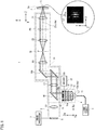
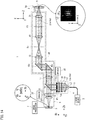
- Fig. 1 is a diagram illustrating a microscope and an optical path of excitation light according to the first embodiment.
- a microscope 1 is assumed to be a scanning type fluorescence microscope, but the microscope according to the embodiment is not limited to a scanning type microscope or a fluorescence microscope.
- the microscope 1 includes a stage 2, a light source 3, an illumination optical system 4, a detection optical system 5, a detection device 6, and an image processor 7.
- the microscope 1 operates as follows in brief.
- the stage 2 holds a sample S as an observation target.
- the sample S is a cell and the like subjected to fluorescent staining in advance.
- the sample S contains a fluorescent substance such as a fluorescent dye.
- the light source 3 emits excitation light L1 that excites the fluorescent substance contained in the sample S.
- the illumination optical system 4 scans the sample S in a plurality of directions (for example, the X-direction and the Y-direction) with interference fringes L2 of the excitation light L1.
- the illumination optical system 4 two-dimensionally scans the sample S with the interference fringes L2.
- the detection optical system 5 is disposed at a position on which fluorescence L3 (illustrated in Fig. 4 described later) from the sample S is incident.
- the detection device 6 includes a plurality of detectors 6a (illustrated in Fig. 4 described later) that detect the fluorescence L3 from the sample S via the detection optical system 5.
- the image processor 7 generates an image (for example, a super resolution image) using detection results obtained by two or more of the detectors 6a of the detection device 6. The following describes respective parts of the microscope 1.
- the light source 3 includes, for example, a light source such as a laser element.
- the light source 3 generates coherent light of a predetermined wavelength band.
- the predetermined wavelength band is set to be a wavelength band including an excitation wavelength of the sample S.
- the excitation light L1 emitted from the light source 3 is, for example, linearly polarized light.
- a light guide member such as an optical fiber 11 is connected to an emitting port of the light source 3.
- the microscope 1 does not necessarily include the light source 3, and the light source 3 may be provided separately from the microscope 1.
- the light source 3 may be disposed in the microscope 1 in a replaceable (attachable, or removable) manner.
- the light source 3 may be externally mounted on the microscope 1 at the time of observation by the microscope 1.
- the illumination optical system 4 is disposed at a position on which the excitation light L1 from the light source 3 is incident.
- the excitation light L1 is incident on the illumination optical system 4 from the light source 3 via the optical fiber 11.
- the optical fiber 11 may be part of the illumination optical system 4 or may be part of a light source device including the light source 3.
- the illumination optical system 4 includes a collimator lens 12, a ⁇ /4 wave plate 13, a polarizer 14, a mask 15 (opening member), a dichroic mirror 16, a relay optical system 17, a scanning part 18, a lens 19, a lens 20, and an objective lens 21 in this order from the light source 3 side toward the sample S side.
- each of the X-direction and the Y-direction is a direction perpendicular to an optical axis 21a of the objective lens 21.
- the Z-direction is a direction parallel with the optical axis 21a of the objective lens 21.
- the optical axis 21a of the objective lens 21 is included in an optical axis 4a of the illumination optical system 4.
- a direction corresponding to each of the X-direction, the Y-direction, and the Z-direction is represented by adding a subscript.
- the Xa-direction, the Ya-direction, and the Za-direction in Fig. 1 are directions respectively corresponding to the X-direction, the Y-direction, and the Z-direction on the optical path from the collimator lens 12 to the dichroic mirror 16.
- the collimator lens 12 converts the excitation light L1 emitted from the optical fiber 11 into parallel light.
- the collimator lens 12 is disposed so that a focal point thereof on the same side as the light source 3 is aligned with a light emitting port of the optical fiber 11.
- a focal point of the lens included in the illumination optical system 4 on the same side as the light source 3 is referred to as a rear side focal point
- a focal point thereof on the same side as the sample S is referred to as a front side focal point as appropriate.
- the ⁇ /4 wave plate 13 causes the polarization state of the excitation light L1 to be circular polarization.
- the polarizer 14 is, for example, a polarizing plate, and has a characteristic of transmitting linearly polarized light in a predetermined direction.
- the polarizer 14 is disposed so that light incident on the sample S becomes S-polarized light (linearly polarized light in the Y-direction).
- the polarizer 14 can rotate about an optical axis 12a of the collimator lens 12.
- the optical axis 12a of the collimator lens 12 is included in the optical axis 4a of the illumination optical system 4.
- the mask 15 is a light flux splitter that splits excitation light that excites a fluorescent substance into a plurality of light fluxes.
- the illumination optical system 4 scans the sample S with the interference fringes L2 that are generated by interference of two or more of the light fluxes split by the mask 15.
- the mask 15 is disposed at a position of a pupil conjugate plane P1 that is optically conjugate to a pupil plane P0 of the objective lens 21, or within a range distant therefrom by 100 mm or less.
- the mask 15 may also be disposed on the pupil plane P0, or within a range distant therefrom by 100 mm or less.
- the mask 15 has an opening 15a and an opening 15b through which the excitation light L1 passes.
- the interference fringes L2 are formed by interference between excitation light L1a passed through the opening 15a and excitation light L1b passed through the opening 15b.
- the mask 15 can rotate about the optical axis 12a of the collimator lens 12.
- the mask 15 is, for example, fixed relatively to the polarizer 14, and rotates integrally with the polarizer 14.
- the mask 15 and the polarizer 14 are rotated by torque supplied from a driver 22.
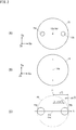
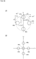
- Fig. 2(A) is a diagram illustrating the mask according to the first embodiment.
- the opening 15a and the opening 15b of the mask 15 are disposed symmetrically to the optical axis 12a of the collimator lens 12 (refer to Fig. 1 ).
- the opening 15a and the opening 15b are arranged in the Xa-direction.
- Fig. 2(B) is a diagram illustrating the polarizer according to the first embodiment.
- a transmission axis 14a of the polarizer 14 is set to be parallel with a direction (in Fig. 2(B) , the Ya-direction) perpendicular to the direction in which the opening 15a and the opening 15b are arranged (in Fig.
- Fig. 2(C) is a diagram illustrating the pupil plane P0 of the objective lens 21.
- Each of the reference numerals P0a and P0b denotes a region on which the excitation light L1 is incident. Parameters illustrated in Fig. 2(C) will be referred to later in the description about the image processor 7.
- the dichroic mirror 16 has a characteristic of reflecting the excitation light L1, and transmitting the fluorescence L3 (illustrated in Fig. 4 described later) from the sample S.
- the excitation light L1 passed through the opening 15a and the opening 15b of the mask 15 is reflected by the dichroic mirror 16, the optical path thereof is bent, and the excitation light L1 is incident on the relay optical system 17.
- the relay optical system 17 guides the excitation light L1 from the dichroic mirror 16 to the scanning part 18.
- the relay optical system 17 is represented as one lens in the drawing, but the number of lenses included in the relay optical system 17 is not limited to one.
- the relay optical system 17 may be unnecessary depending on a distance and the like of the optical system. In the respective drawings, two or more lenses may be represented as one lens for a portion other than the relay optical system 17.
- the scanning part 18 scans the sample S with the interference fringes L2 of the excitation light L1 in two directions including the X-direction and the Y-direction.
- the scanning part 18 changes positions at which the interference fringes L2 are formed by the excitation light L1 in two directions intersecting with the optical axis 21a of the objective lens 21.
- the scanning part 18 includes a deflecting mirror 18a and a deflecting mirror 18b. Inclination of the deflecting mirror 18a and the deflecting mirror 18b with respect to the optical path of the excitation light L1 is variable.
- Each of the deflecting mirror 18a and the deflecting mirror 18b is a galvanometer mirror, a MEMS mirror, a resonant mirror (resonance type mirror), and the like.
- Each of the deflecting mirror 18a and the deflecting mirror 18b may be a scanner.
- the deflecting mirror 18a changes, in the X-direction, a position on the sample S on which the excitation light L1 is incident.
- the deflecting mirror 18b changes, in the Y-direction, a position on the sample S on which the excitation light L1 is incident.
- the scanning part 18 is, for example, disposed so that a position that is conjugate to the pupil plane P0 of the objective lens 21 becomes the position of the deflecting mirror 18a, the position of the deflecting mirror 18b, or a position between the deflecting mirror 18a and the deflecting mirror 18b.
- the scanning part 18 may have a configuration in which the position on the sample S on which the excitation light L1 is incident is changed in the Y-direction by the deflecting mirror 18a, and changed in the X-direction by the deflecting mirror 18b.
- the excitation light L1 from the scanning part 18 is incident on the lens 19.
- the lens 19 concentrates the excitation light L1 to a sample conjugate plane Sb that is optically conjugate to a sample plane Sa of the objective lens 21.
- the sample plane Sa is a plane disposed at the front side focal point of the objective lens 21 or a position in the vicinity of the front side focal point, and perpendicular to the optical axis 21a of the objective lens 21.
- interference fringes are formed by interference between the excitation light L1a passed through the opening 15a of the mask 15 and the excitation light L1b passed through the opening 15b.
- the excitation light L1 passed through the sample conjugate plane Sb is incident on the lens 20.
- the lens 20 converts the excitation light L1 into parallel light.
- the excitation light L1 passed through the lens 20 passes through the pupil plane P0 of the objective lens 21.
- the objective lens 21 concentrates the excitation light L1 onto the sample plane Sa.
- the lens 20 and the objective lens 21 project, on the sample plane Sa, the interference fringes formed on the sample conjugate plane Sb.
- the interference fringes L2 are locally formed on the sample plane Sa.
- the interference fringes L2 include a bright part having relatively high light intensity and a dark part having relatively low light intensity.
- a direction in which the bright part and the dark part are arranged (in Fig. 1 , the X-direction) is referred to as a periodic direction D1 of the interference fringes L2 as appropriate.
- the periodic direction D1 of the interference fringes L2 corresponds to the direction in which the opening 15a and the opening 15b of the mask 15 are arranged (in Fig. 1 , the Xa-direction).
- the driver 22 causes the mask 15 to rotate about the Za-direction
- the direction in which the opening 15a and the opening 15b are arranged is rotated
- the periodic direction D1 of the interference fringes L2 is rotated about the Z-direction.
- the driver 22 is included in a fringe direction changer that changes the direction of the interference fringes L2.
- the driver 22 changes a direction in which two or more light fluxes are arranged (hereinafter, referred to as a light flux splitting direction) on a plane perpendicular to the optical axis 4a of the illumination optical system 4 (for example, a plane on a light emitting side of the mask 15).
- the light flux splitting direction described above is, for example, the direction in which the opening 15a and the opening 15b are arranged, and the driver 22 causes the mask 15 to rotate to change the light flux splitting direction.
- the driver 22 causes the polarizer 14 to rotate interlocking with the mask 15 to change orientation of the transmission axis of the polarizer 14 and adjusts the excitation light L1 to be incident on the sample S as S-polarized light. That is, the polarizer 14 and the driver 22 are included in a polarization adjuster that adjusts the polarization state of the excitation light L1 on the basis of the direction of the interference fringes.
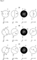
- Fig. 3 is a diagram illustrating the mask, the polarizer, the interference fringes, and the polarization state of the excitation light according to the first embodiment.
- the direction in which the opening 15a and the opening 15b of the mask 15 are arranged is the Xa-direction.
- the transmission axis 14a of the polarizer 14 is the Ya-direction perpendicular to the Xa-direction.
- the light flux of the excitation light L1 (refer to Fig. 1 ) passed through the opening 15a and the light flux thereof passed through the opening 15b are incident on the sample S, and the interference fringes L2 in the periodic direction D1 are generated.
- the excitation light L1 incident plane is parallel with the XZ-plane.
- a polarization direction D2 thereof is the Y-direction perpendicular to the incident plane. That is, the excitation light L1 is incident on the sample S as S-polarized light.
- the direction in which the opening 15a and the opening 15b of the mask 15 are arranged is a direction obtained by rotating the Xa-direction counterclockwise by 120°.
- the transmission axis 14a of the polarizer 14 is a direction obtained by rotating the Ya-direction counterclockwise by 120°.
- the periodic direction of the interference fringes L2 is a direction forming an angle of 120° with respect to the X-direction.
- the incident plane of the excitation light L1 is a plane obtained by rotating the XZ-plane about the Z-direction by 120°.
- the polarization direction D2 thereof is a direction perpendicular to the incident plane. That is, the excitation light L1 is incident on the sample S as S-polarized light.
- the direction in which the opening 15a and the opening 15b of the mask 15 are arranged is a direction obtained by rotating the Xa-direction counterclockwise by 240°.
- the transmission axis 14a of the polarizer 14 is a direction obtained by rotating the Ya-direction counterclockwise by 240°.
- the periodic direction D1 of the interference fringes L2 is a direction forming an angle of 240° with respect to the X-direction.
- the incident plane of the excitation light L1 is a plane obtained by rotating the XZ-plane about the Z-direction by 240°.
- the polarization direction D2 thereof is a direction perpendicular to the incident plane. That is, the excitation light L1 is incident on the sample S as S-polarized light.
- the periodic direction of the interference fringes L2 is changed in three patterns in units of an angle of 120°, but the periodic direction of the interference fringes L2 is not limited to this example.
- the periodic direction of the interference fringes L2 corresponds to a direction in which resolving power can be improved (a direction in which a super resolution effect can be obtained) in an image generated by the image processor 7 (described later).
- the periodic direction of the interference fringes L2 is appropriately set so that a desired super resolution effect can be obtained.
- the mask 15 may be replaceable in accordance with magnification, a numerical aperture (NA) of the objective lens 21, and an illumination pupil shape.
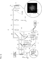
- Fig. 4 is a diagram illustrating the microscope and an optical path of fluorescence according to the first embodiment.
- the detection optical system 5 forms an image of the fluorescence L3 generated in the sample S.
- the detection optical system 5 includes the objective lens 21, the lens 20, the lens 19, the scanning part 18, the relay optical system 17, the dichroic mirror 16, and a lens 23 in this order from the sample S side toward the detection device 6 side.
- the fluorescence L3 generated in the sample S passes through the objective lens 21, the lens 20, and the lens 19 in this order, and is incident on the scanning part 18.
- the fluorescence L3 is descanned by the scanning part 18 and passes through the relay optical system 17 to be incident on the dichroic mirror 16.
- the dichroic mirror 16 has a characteristic of transmitting the fluorescence L3.
- the fluorescence L3 transmitted through the dichroic mirror 16 is incident on the lens 23.
- the lens 23 concentrates the fluorescence L3 to the detection device 6.
- the detection device 6 is an image sensor and includes the detectors 6a that are two-dimensionally arranged.
- the detectors 6a are arranged in two directions in the detection device 6.
- the detectors 6a are arranged in two directions including the Xb-direction and the Yb-direction.
- Each of the detectors 6a is a sensor cell, a pixel, a photodetector, or the like including a photoelectric conversion element such as a photodiode.
- Each of the detectors 6a can detect the fluorescence L3.
- the detector 6a corresponds to one pixel, but a detection region (light receiving region) including a plurality of pixels may be used as one detector 6a.
- the microscope 1 scans the interference fringes L2 on the sample plane Sa with the scanning part 18, and the detection device 6 detects the fluorescence L3.
- the microscope 1 illuminates an illumination region selected from the sample plane Sa with the interference fringes L2, and the detection device 6 detects the fluorescence L3 from the illumination region.
- the microscope changes the illumination region with the scanning part 18.
- the microscope 1 repeatedly performs the processing of detecting the fluorescence and the processing of changing the illumination region to acquire fluorescence intensity distribution (a measurement value obtained by the detection device 6) in a desired region.
- the image processor 7 generates an image on the basis of a detection result that is obtained by the detection device 6 as described above.
- a wave number may be referred to as a space frequency or a frequency.
- the magnification of the optical system is assumed to be 1 for convenience of explanation, but the magnification may be optionally set.
- a pupil radius k NA ex of the objective lens 21 in a case in which the excitation light is incident and a pupil radius k NA em of the objective lens 21 in a case in which the fluorescence is incident are represented by the following expression (1).
- electric field amplitudes of the pupil plane and an image plane are related to each other on the basis of a relation of Fourier transformation, so that the coordinates of a pupil position may be represented by wave coordinates.
- Each of k NA ex and k NA em indicates a value of the pupil radius in a case in which the pupil is represented by the wave coordinates.
- the pupil plane P0 is represented in a wave coordinate space (frequency space).
- An inside region of a circle illustrated by a dotted line in Fig. 2(C) is a pupil of the objective lens 21, and k NA ex is a pupil radius of the objective lens 21.
- Each of a region P0a and a region P0b on which the excitation light L1 is incident is assumed to have a circular shape but does not necessarily have the circular shape.
- a radius of each of the region P0a and the region P0b is ⁇ k NA ex .
- ⁇ is a ratio of the radius of the region P0a or the region P0b to the pupil radius of the objective lens 21.
- a distance from the optical axis 21a of the objective lens 21 to the center of the region P0a is (1 - ⁇ ) k NA ex .
- a distance between the center of the region P0a and the center of the region P0b is, for example, 2(1 - ⁇ )k NA ex , but is not limited to this value.
- Electric field intensity ill(r) of the excitation light on the sample plane Sa is represented by the following expression (2).
- Expression (2) ill r PSF ill r 1 + cos 2 ⁇ k 0 ⁇ r 2
- PSF ill (r) is a point spread function in a case in which the numerical aperture of the optical system is ⁇ NA.
- the interval between the interference fringes is referred to as a fringe interval or a period of the interference fringes as appropriate.
- the fluorescent substance contained in the sample S is excited by the excitation light L1, and the fluorescence L3 is emitted from the excited fluorescent substance.
- the detection device 6 receives the fluorescence L3 and takes an image of the fluorescent substance formed by the detection optical system 5.
- the detection device 6 takes the image of the fluorescent substance to acquire image data.
- the size of the detector 6a (detector size) of the detection device 6 is assumed to be sufficiently smaller than a dimension corresponding to the period of the interference fringes L2 in the detection device 6 (a length on the detection device 6 corresponding to one period).
- the size of the detector 6a is set to be about ⁇ em /4NA.
- I(r,r s ) distribution of the fluorescent substance in the sample S is represented as Obj(r), and the image data obtained by the detection device 6 is represented as I(r,r s ).
- I(r,r s ) is represented by the following expression (3).
- I r r s PSF det r ⁇ r Obj r + r s ill r
- *r is a convolution of r.
- PSF det (r) is a detection PSF defined by the detection optical system 5 including the objective lens 21 and the fluorescence wavelength ⁇ em .
- the following expression (4) is obtained by deforming I(r,r s ).
- PSF eff (r,r s ) is an effective PSF defined in the following expression (5).
- Fig. 5 is a diagram illustrating the effective PSF for each detector of the detection device according to the first embodiment.
- a horizontal axis indicates the Xb-direction of the detection device 6.
- Fig. 5(A) illustrates a graph representing the effective PSF (solid line) of each of three detectors 6a having different coordinates in the Xb-direction.
- the graph at the center of Fig. 5(A) represents distribution Q1a (solid line) corresponding to the effective PSF of the detector 6a disposed at a position X1a.
- the graph on the left side of Fig. 5(A) represents distribution Q1b (solid line) corresponding to the effective PSF of the detector 6a disposed at a position X1b.
- the graph on the right side of Fig. 5(A) represents distribution Q1c (solid line) corresponding to the effective PSF of the detector 6a disposed at a position X1c.
- the reference numeral Q2 corresponding to a dotted line in Fig. 5 denotes distribution corresponding to intensity distribution of the interference fringes L2 illustrated in Fig. 2 , for example.
- the distribution Q2 corresponds to the electric field intensity ill(r) (refer to the expression (2) described above) of the excitation light on the sample plane Sa.
- Positions at which the intensity of the interference fringes L2 becomes a maximum, that is, peak positions X2a, X2b, and X2c of the distribution Q2 can be obtained by numerical simulation and the like in advance.
- the distribution Q2 includes Q2a, Q2b, and Q2c as partial distribution.
- the distribution Q2a is distribution in a range from a minimum position before the peak position X2a to the next minimum position.
- the distribution Q2b is distribution in a range from a minimum position before the peak position X2b to the next minimum position.
- the distribution Q2c is distribution in a range from a minimum position before the peak position X2c to the next minimum position.
- the reference numerals Q3a, Q3b, and Q3c corresponding to a chain double-dashed line in Fig. 5 denote distribution corresponding to the detection PSF defined by the detection optical system 5 including the objective lens 21 and the fluorescence wavelength ⁇ em .
- the detection PSF corresponds to PSF det (r) in the expression (3) and the like.
- the distribution Q3a represented by a graph at the center of Fig. 5(A) is distribution corresponding to the detector 6a disposed at the position X1a among the detectors 6a.
- the distribution Q3a becomes a maximum (reaches a peak) at the position X1a at which the detector 6a is disposed (for example, the center position in the light receiving region of the detector 6a).
- the position X1a is substantially the same as the peak position X2a of the distribution Q2a corresponding to the intensity distribution of the interference fringes L2.
- the distribution Q1a corresponding to the effective PSF is distribution obtained by multiplying the distribution Q2 corresponding to the intensity distribution of the interference fringes L2 by the distribution Q3a corresponding to the detection PSF of the detector 6a disposed at the position X1a.
- a deviation amount of the position X1a of the detector 6a that is, the peak position of the detection PSF (the peak position of the distribution Q3a) from the peak position X2a of the distribution Q2a corresponding to the intensity distribution of the interference fringes L2 is smaller than a predetermined value (for example, substantially 0).
- a predetermined value for example, substantially 0
- the distribution Q1a of the effective PSF takes a single maximum (peak).
- the peak position of the distribution Q1a is substantially the same as the position X1a of the detector 6a or the peak position X2a of the distribution Q2a corresponding to the intensity distribution of the interference fringes L2.
- the distribution Q3b represented by the graph on the left side of Fig. 5(A) is distribution corresponding to the detector 6a disposed at the position X1b among the detectors 6a.
- the distribution Q3b becomes a maximum (reaches a peak) at the position X1b at which the detector 6a is disposed (for example, the center position in the light receiving region of the detector 6a).
- the position X1b deviates from the peak position X2b of the partial distribution Q2b including the position X1b of the distribution Q2 corresponding to the intensity distribution of the interference fringes L2.
- the distribution Q1b corresponding to the effective PSF is distribution obtained by multiplying the distribution Q2 corresponding to the intensity distribution of the interference fringes L2 by the distribution Q3b corresponding to the detection PSF of the detector 6a disposed at the position X1b.
- a shift amount of the position X1b of the detector 6a that is, the peak position of the detection PSF (the peak position of the distribution Q3b) from the peak position X2b of the distribution Q2b corresponding to the intensity distribution of the interference fringes L2 is larger than the predetermined value.
- the distribution Q1b of the effective PSF takes two maxima (peaks).
- the peak of the effective PSF is caused to branch into two peaks depending on the position of the detector 6a in some cases, and this phenomenon is called distortion of the shape of the effective PSF.
- a peak at which the effective PSF is the strongest is called a main lobe, and the other peaks are called side lobes.
- the peak position of the main lobe of the distribution Q1b of the effective PSF deviates from the center position of the detection device 6 (the position of X2a, the position of the optical axis of the detection optical system). In this way, it can be found that the position of the main lobe of the effective PSF deviates depending on the position (r) of the detector 6a of the detection device 6.
- a deviation in the position of the main lobe of the effective PSF is called a positional deviation of the effective PSF as appropriate.
- the distribution Q3c represented by the graph on the right side of Fig. 5(A) is distribution corresponding to the detector 6a disposed at the position X1c among the detectors 6a.
- the distribution Q3c becomes a maximum (reaches a peak) at the position X1c at which the detector 6a is disposed (for example, the center position in the light receiving region of the detector 6a).
- the position X1c deviates from the peak position X2c of the partial distribution Q2c including the position X1c of the distribution Q2 corresponding to the intensity distribution of the interference fringes L2.
- the distribution Q1c corresponding to the effective PSF is distribution obtained by multiplying the distribution Q2 corresponding to the intensity distribution of the interference fringes L2 by the distribution Q3c corresponding to the detection PSF of the detector 6a disposed at the position X1c.
- a deviation of the position X1c of the detector 6a that is, the peak position of the detection PSF (the peak position of the distribution Q3c) from the peak position X2c of the distribution Q2c corresponding to the intensity distribution of the interference fringes L2 is larger than the predetermined value.
- the distribution Q1b of the effective PSF takes two maxima (peaks), and distortion of the shape of the effective PSF and a positional deviation of the effective PSF are caused.
- Fig. 5(B) is different from Fig. 5(A) in the position of the detector 6a.
- Distribution Q3d represented by the graph on the left side of Fig. 5(B) is distribution corresponding to the detector 6a disposed at a position X1d among the detectors 6a.
- the distribution Q3d becomes a maximum (reaches a peak) at the position X1d at which the detector 6a is disposed (for example, the center position in the light receiving region of the detector 6a).
- the position X1d is substantially the same as the peak position X2b of the partial distribution Q2b including the position X1d of the distribution Q2 corresponding to the intensity distribution of the interference fringes L2.
- the distribution Q1d of the effective PSF takes a single maximum (peak), and the peak position of the distribution Q1d is substantially the same as the position X1d of the detector 6a or the peak position X2b of the distribution Q2b corresponding to the intensity distribution of the interference fringes L2. That is, distortion of the shape of the effective PSF is not caused.
- Distribution Q3e represented by the graph on the right side of Fig. 5(B) is distribution corresponding to the detector 6a disposed at a position X1e among the detectors 6a.
- the distribution Q3e becomes a maximum (reaches a peak) at the position X1e at which the detector 6a is disposed (for example, the center position in the light receiving region of the detector 6a).
- the position X1e is substantially the same as the peak position X2c of the partial distribution Q2c including the position X1e of the distribution Q2 corresponding to the intensity distribution of the interference fringes L2.
- the distribution Q1e of the effective PSF takes a single maximum (peak), and the peak position of the distribution Q1e is substantially the same as the position X1e of the detector 6a or the peak position X2c of the distribution Q2c corresponding to the intensity distribution of the interference fringes L2. That is, distortion of the shape of the effective PSF is not caused.
- the image processor 7 uses a detection result of the detector 6a that is selected from among the detectors 6a on the basis of the magnification of the detection optical system 5 and the period of the interference fringes L2 (fringe interval).
- the image processor 7 selects the detector 6a from among the detectors 6a on the basis of the peak position of the interference fringes L2 (for example, the peak positions X2a, X2b, and X2c in Fig. 5 ), and uses a detection result of the selected detector 6a.
- the peak position of the interference fringes L2 corresponds to, for example, a position at which the intensity is maximum in the intensity distribution of the interference fringes L2 (for example, the center position of the bright part).
- the image processor 7 uses a detection result of the detector 6a disposed at the position X1a corresponding to the peak position X2a as a detection result corresponding to the peak position X2a in the graph at the center of Fig. 5(B) .
- the peak positions X2a, X2b, and X2c are obtained in advance by numerical simulation and the like and stored in a storage in advance.
- the image processor 7 selects the detector 6a that is disposed to be the closest to the peak position X2a from among the detectors 6a on the basis of the stored information about the peak positions and uses a detection result of the selected detector 6a.
- the image processor 7 may use only a detection result of one detector 6a disposed at the position X1a, or may use detection results of the detector 6a disposed at the position X1a and at least one detector 6a around the former detector 6a.
- the image processor 7 uses a detection result of the detector 6a disposed at the position X1d corresponding to the peak position X2b. On the basis of the magnification of the detection optical system 5 and the period of the interference fringes L2, the image processor 7 selects, from among the detectors 6a, the detector 6a the position of which matches the partial distribution Q2b including one peak of the intensity distribution of the interference fringes L2.
- the image processor 7 selects, from among the detectors 6a, the detector 6a that is disposed to be the closest to the peak position X2b (for example, the detectors 6a disposed at the position X1d).
- the image processor 7 uses a detection result of the selected detector 6a as a detection result related to the distribution Q2b.
- the image processor 7 may use only a detection result of one detector 6a disposed at the position X1d, or may use detection results of the detector 6a disposed at the position X1d and at least one detector 6a around the former detector 6a.
- the effective PSF (PSF eff ) corresponding to the distribution Q1d distortion of the shape of the effective PSF is suppressed when the peak position X2b of the distribution Q2b matches the position X1d of the detector 6a.
- the image processor 7 uses a detection result of the detector 6a disposed at the position X1e corresponding to the peak position X2c. On the basis of the magnification of the detection optical system 5 and the period of the interference fringes L2, the image processor 7 selects, from among the detectors 6a, the detector 6a the position of which matches the partial distribution Q2c including one peak of the intensity distribution of the interference fringes L2.
- the image processor 7 selects, from among the detectors 6a, the detector 6a that is disposed to be the closest to the peak position X2c (for example, the detector 6a disposed at the position X1e).
- the image processor 7 uses a detection result of the selected detector 6a as a detection result related to the distribution Q2c.
- the image processor 7 may use only a detection result of one detector 6a disposed at the position X1e, or may use detection results of the detector 6a disposed at the position X1e and at least one detector 6a around the former detector 6a.
- the distribution Q1e PSF eff
- distortion of the shape of the effective PSF is suppressed when the peak position X2c of the distribution Q2c matches the position X1e of the detector 6a.
- the image processor 7 corrects the positional deviation of the image for each detector (the positional deviation of the peak position of the effective PSF eff or the main lobe) in the detection result of the detector 6a that is selected as described above.
- the positional deviation of the image for each detector can be acquired on the basis of theoretical calculation using various design values or a taken image of small objects such as fluorescent beads photographed by the detection device 6. By correcting the positional deviation in this way, effective PSFs of images obtained by the respective selected detectors 6a can be caused to be substantially the same.
- the PSF eff of the image that is obtained as described above can be assumed to be approximately equivalent to the PSF eff of the detector at the center position of the detection device 6 (the detector positioned on the optical axis).
- the full width at half maximum of the PSF becomes 1.4 times narrower and resolving power is improved as compared with the conventional fluorescence microscope.
- the full width at half maximum of the PSF of the confocal microscope is preferably 1.5 times or more narrower as compared with the conventional fluorescence microscope. That is, the number of bright parts included in the periodic direction of the interference fringes L2 according to the embodiment is preferably equal to or larger than 3. The same applies to the other embodiments.
- the image processor 7 generates an image by adding up images the PSF eff of which becomes substantially the same.
- the image processor 7 can generate an image I SR (r s ) having favorable resolving power and a favorable S/N ratio when the images that are added up have substantially the same PSF eff .
- a signal amount can be increased.
- a sectioning capacity can be enhanced.
- the OTF is expanded in the direction of the interference fringes L2, and the microscope has a cutoff frequency up to 2k cut conv .
- the excitation wavelength and the fluorescence wavelength are equally assumed to be ⁇ herein.
- the OTF according to the embodiment is obtained by combining the OTF of the conventional fluorescence microscope with a component that is the OTF of the conventional fluorescence microscope shifted in the periodic direction of the interference fringes L2.
- the resolving power in the periodic direction of the interference fringes L2 (in Fig. 1 , the X-direction) is improved.
- the microscope 1 can also two-dimensionally improve the resolving power by changing the periodic direction of the interference fringes L2 and detecting fluorescence from the sample S.
- the following describes an example of changing the periodic direction of the interference fringes L2 by 90°.
- the mask 15 and the polarizer 14 in the state of Fig. 2 are rotated about the Za-direction by 90°.
- a super resolution image in a case in which the periodic direction of the interference fringes L2 is the X-direction is assumed to be I SRx (r s )
- a super resolution image in a case in which the periodic direction of the interference fringes L2 is the Y-direction is assumed to be I SRy (r s ).
- the image processor 7 may generate the super resolution image the resolving power of which is two-dimensionally improved by adding up I SRx (r s ) and I SRy (r s ).
- the image processor 7 may also generate the super resolution image by performing the following processing.
- the image processor 7 performs Fourier transformation on each of the super resolution image I SRx (r s ) and the super resolution image I SRy (r s ).
- the super resolution image I SRx (r s ) subjected to the Fourier transformation is represented as I ⁇ SRx (k s ).
- " ⁇ " is a tilde in numerical expressions.
- the super resolution image I SRy (r s ) subjected to the Fourier transformation is represented as I ⁇ SRy (k s ).
- the cutoff frequency of I ⁇ SR_x (k s ) is increased in the periodic direction (X-direction) of the interference fringes as compared with the conventional fluorescence microscope.
- the cutoff frequency of I ⁇ SRy (k s ) is increased in the periodic direction (Y-direction) of the interference fringes as compared with the conventional fluorescence microscope.
- the image processor 7 adds up I ⁇ SRx (k s ) and I ⁇ SRy (k s ). Due to this, the cutoff frequency is increased in two directions (the X-direction and the Y-direction).
- the shape of the added effective OTF may be distorted depending on a combination of directions in which the periodic direction of the interference fringes L2 is changed.
- the image processor 7 may apply a frequency filter to correct the shape of the effective OTF. Due to this, the resolving power can be improved more effectively than the case of adding up I SRx (r s ) and I SRy (r s ).
- the illumination optical system 4 may change the periodic direction of the interference fringes L2 into three patterns including 0°, 120°, and 240°, and the detection device 6 may detect the fluorescence L3 for each of the three patterns of periodic directions.
- the image processor 7 may generate the super resolution image for three patterns of periodic directions using three detection results (for example, three images) detected by the detection device 6.
- Fig. 6 is a flowchart illustrating the observation method according to the embodiment.
- the illumination optical system 4 in Fig. 1 sets an angle of a scanning mirror.
- the illumination optical system 4 irradiates a position on the sample that is defined on the basis of the angle of the scanning mirror set in Step S1 with excitation light as the interference fringes.
- Step S2 a fluorescent substance of the sample is excited by the interference fringes of the excitation light.
- the detection device 6 in Fig. 4 detects the fluorescence L3 from the sample S via the detection optical system 5.
- Step S4 the microscope 1 (for example, a controller) determines whether to change the angle of the scanning mirror. If it is determined that the processing from Step S1 to Step S3 is not ended for part of planned observation regions, the microscope 1 determines to change the angle of the scanning mirror in Step S4 (Yes in Step S4). If it is determined to change the angle of the scanning mirror (Yes in Step S4), the microscope 1 returns the process to the processing in Step S1, and the illumination optical system 4 sets the angle of the scanning mirror to be the next planned angle. The processing from Step S2 to Step S4 is then repeated. In this way, the illumination optical system 4 two-dimensionally scans the sample S with the interference fringes of the excitation light L1.
- Step S4 if it is determined that the processing from Step S1 to Step S3 is ended for all of the planned observation regions, the microscope 1 determines not to change the angle of the scanning mirror (No in Step S4). If the microscope 1 determines not to change the angle of the scanning mirror (No in Step S4), the image processor 7 corrects the positional deviation of the image for each detector in Step S5.
- the image processor 7 corrects data obtained from at least one of the detectors on the basis of the position of the detector. For example, the image processor 7 corrects data obtained from the detector that is selected from among the detectors on the basis of the position of the detector. For example, the image processor 7 corrects data obtained from a first detector in the detectors (for example, the detector disposed at the position X1d in Fig.
- the image processor 7 generates an image using detection results of two or more detectors. For example, in Step S6, the image processor 7 generates an image (for example, a super resolution image) by adding up the images corrected in Step S5.
- the positions of the detectors 6a of the detection device 6 may be set on the basis of the period of the interference fringes L2 to be matched with the peak (or maximum, bright point) position of the interference fringes L2.
- the detection device 6 may be set in advance so that an interval between the detectors 6a matches the fringe interval of the interference fringes L2.
- the interval between the detectors 6a described above is an interval between the center of one detector 6a and the center of the detector 6a adjacent thereto.
- the fringe interval of the interference fringes L2 described above is an interval between a center line of one bright part and a center line of a bright part adjacent thereto in the interference fringes L2.
- the fringe interval of the interference fringes L2 is 1/k 0 .
- the interval between the detectors 6a of the detection device 6 is set to be substantially the same as P represented by the following expression (7).
- the magnification of the detection optical system 5 including the objective lens 21 is assumed to be 1.
- the interval between the detectors 6a may be changed corresponding to the magnification to cause the interval between the detectors 6a to be M det /k0.
- the interval between the detectors 6a can be caused to match the period of the interference fringes L2 by causing part of the detection optical system 5 to be a zoom lens.
- the period of the interference fringes L2 may be adjusted to match the interval between the detectors 6a of the detection device 6.
- the period of the interference fringes L2 can be changed by changing an interval between the openings 15a and 15b of the mask 15.
- the microscope 1 two-dimensionally scans the interference fringes L2 by scanning the interference fringes L2 in two directions that are parallel with the sample plane Sa.
- the microscope 1 according to the embodiment may three-dimensionally scan the interference fringes L2 by scanning the interference fringes L2 in two directions parallel with the sample plane Sa and in one direction perpendicular to the sample plane Sa.
- processing of scanning the interference fringes L2 in two directions parallel with the sample plane Sa (hereinafter, referred to as two-dimensional processing) is the same as the processing described in the embodiment described above.
- the microscope 1 can generate a three-dimensional super resolution image.
- the microscope 1 may similarly three-dimensionally scan the interference fringes L2.
- the image processor 7 (refer to Fig. 4 ) performs filtering on data in the frequency space to generate an image.
- the image processor 7 performs deconvolution on the data obtained from the detection device 6 to generate the image.
- the image processor 7 performs deconvolution and apodization for each detector 6a of the detection device 6 to generate the image. That is, the image processor 7 performs filtering including deconvolution on the data in the frequency space.
- a series of processing including deconvolution and apodization may be collectively referred to as deconvolution as appropriate.
- Fig. 7 is a diagram illustrating processing performed by the image processor of the microscope according to the second embodiment.
- Fig. 7(A) illustrates the PSF before deconvolution, which is the same as that in Fig. 5(A) .
- the interval between the detectors 6a of the detection device 6 does not match the interval of the interference fringes L2.
- the shape of the effective PSF (solid line) of the image obtained for each detector 6a may be distorted depending on the position of the detector 6a.
- the effective PSF for each detector 6a can be acquired (estimated) by performing theoretical calculation on the basis of the design value or imaging small objects such as fluorescent beads.
- the image processor 7 performs deconvolution to correct distortion of the shape of the effective PSF of the image that is obtained for each detector 6a and the positional deviation thereof.
- Fig. 7(B) illustrates the PSF after deconvolution.
- the reference numeral Q4a corresponds to the effective PSF that is obtained by performing deconvolution on the distribution Q1a represented by the graph at the center of Fig. 7(A) , that is, the effective PSF of the detector 6a disposed at the position X1a.
- the deviation amount between the position X1a of the detector 6a and the peak position X2a of the distribution Q2a is smaller than a predetermined value, and the distribution Q4a corresponding to the effective PSF after deconvolution is substantially the same as the distribution Q1a corresponding to the effective PSF before deconvolution.
- the reference numeral Q4b corresponds to the effective PSF that is obtained by performing deconvolution on the distribution Q1b represented by the graph on the left side of Fig. 7(A) , that is, the effective PSF of the detector 6a disposed at the position X1b.
- the reference numeral Q4c corresponds to the effective PSF that is obtained by performing deconvolution on the distribution Q1c represented by the graph on the right side of Fig. 7(A) , that is, the effective PSF of the detector 6a disposed at the position X1c.
- the image processor 7 generates an image using a result of deconvolution. The following describes processing performed by the image processor 7 in more detail.
- the image processor 7 converts at least some of the detection results of the detectors 6a into data in the frequency space, and generates an image (for example, a super resolution image) using a conversion result thereof.
- the data representing at least some of the detection results of the detectors 6a in the frequency space is referred to as a component of the frequency space as appropriate.
- the image processor 7 performs Fourier transformation on at least some of the detection results of the detectors 6a, and generates the image using the component of the frequency space obtained through the Fourier transformation.
- I ⁇ (r,k s ) on the left side is obtained by performing Fourier transformation on r s of I(r,r s ).
- OTF eff (r,k s ) on the right side is obtained by performing Fourier transformation on r s of PSF eff (r,r s ), and represents the effective OTF for each detector 6a of the detection device 6.
- Obj ⁇ (k s ) on the right side is obtained by performing Fourier transformation on r s of Obj(r s ).
- Deconvolution for each detector using the Wiener filter is represented by the following expression (9).
- Obj ⁇ (r,k s ) is distribution of the fluorescent substance estimated for each detector 6a of the detection device 6 (hereinafter, referred to as estimated fluorescent substance distribution).
- w is a Wiener parameter for suppressing noise.
- the image processor 7 performs apodization on Obj ⁇ (r,k s ) through processing represented by the following expression (10) and adds up spectrums of the detectors 6a of the detection device 6 to generate the super resolution image I SR (r s ).
- I SR r s F k s ⁇ 1 ⁇ r Ob ⁇ j r k s A k s
- A(k s ) is an apodization function for suppressing a negative value of the image, and multiplying Obj ⁇ (r,k s ) by A(k s ) is called apodization.
- a function form of A(k s ) is designed to suppress a negative value of the image by theoretical calculation, simulation, or the like.
- F ks -1 is inverse Fourier transformation of k s .
- the image processor 7 performs inverse Fourier transformation after adding up the spectrums of the respective detectors 6a but may add up the images after performing inverse Fourier transformation. In the processing of the expression (9) and the expression (10), the image processor 7 adds up the images of the respective detectors 6a after independently performing deconvolution for each detector 6a.
- the image processor 7 may collectively perform deconvolution on two or more detectors 6a as represented by the following expression (11).
- I r s F k s ⁇ 1 ⁇ r OTF eff ⁇ r k s I ⁇ r k s ⁇ r OTF eff r k s 2 + w 2 A k s
- Fig. 8 is a flowchart illustrating the observation method according to the second embodiment.
- the processing from Step S1 to Step S4 is the same as that in Fig. 6 , so that description thereof is omitted.
- the image processor 7 performs Fourier transformation on the detection result of each detector.
- the image processor 7 performs deconvolution.
- the image processor 7 performs apodization. Apodization may be processing as part of deconvolution.
- the image processor 7 adds up the images of the respective detectors 6a using a result of deconvolution.
- the image processor 7 performs inverse Fourier transformation on a first image (for example, a Fourier image) obtained in Step S14 to generate a second image (for example, a super resolution image).
- the image processor 7 may change the range of the detectors 6a to be added up.
- the image processor 7 may also one-dimensionally or two-dimensionally improve the resolving power as described above in the first embodiment.
- Fig. 9 is a diagram illustrating processing performed by the image processor of the microscope according to the third embodiment. Regarding the respective parts of the microscope, refer to Fig. 1 or Fig. 4 as appropriate.
- the image processor 7 (refer to Fig. 4 ) corrects distortion of the shape of the effective PSF for each detector 6a through image processing different from that in the second embodiment.
- Fig. 9(A) illustrates the PSF before the image processing according to the present embodiment, which is the same as that in Fig. 5(A) .
- the interval between the detectors 6a of the detection device 6 (refer to Fig. 4 ) does not match the interval of the interference fringes L2.
- the shape of the effective PSF (solid line) of the image obtained for each detector 6a may be distorted depending on the position of the detector 6a.
- the image processor 7 effectively shifts a phase of intensity distribution of the interference fringes L2 through image processing so that the peak position of partial distribution of intensity distribution of the interference fringes L2 (for example, Q2b represented by the graph on the left side of Fig. 9(A) ) matches the position of the detector 6a.
- Fig. 9(B) illustrates the effective PSF for each detector 6a after the phase is shifted.
- distribution Q2f is distribution obtained by shifting the phase of distribution Q2 so that the peak position X2b of the distribution Q2b in Fig. 9(A) matches the position X1b of the detector 6a.
- a peak position X2f of the distribution Q2f substantially matches the position X1b of the detector 6a.
- the reference numeral Q1f denotes distribution corresponding to the effective PSF that is obtained on the basis of the distribution Q2f the phase of which is shifted and the detection PSF (distribution Q3b) of the detector 6a disposed at the position X1b. Distortion of the shape of the effective PSF is reduced for the distribution Q1f.
- distribution Q2g is distribution obtained by shifting the phase of the distribution Q2 so that the peak position X2c of the distribution Q2c in Fig. 9(A) matches the position X1c of the detector 6a.
- a peak position X2g of the distribution Q2g substantially matches the position X1c of the detector 6a.
- the reference numeral Q1g denotes distribution corresponding to the effective PSF that is obtained on the basis of the distribution Q2g the phase of which is shifted and the detection PSF (distribution Q3c) of the detector 6a disposed at the position X1c. Distortion of the shape of the effective PSF is reduced for the distribution Q1g.
- the shapes of the effective PSFs (solid line) of the respective detectors 6a are corrected to be substantially the same.
- the image processor 7 generates an image using the images of the respective detectors 6a having the effective PSFs the shapes of which are corrected to be substantially the same.
- the following describes a processing procedure performed by the image processor 7 in more detail.
- the image I(r,r s ) obtained by the detection device 6 is represented by the expression (3) described above.
- ill(r) represented by the expression (2) described above By substituting ill(r) represented by the expression (2) described above for the expression (3), the following expression (12) is obtained.
- I r r s PSF det r + r s PSF ill r s 1 + cos 2 ⁇ k 0 ⁇ r s + ⁇ 2 ⁇ r s Obj r s
- ⁇ indicates an initial phase of the interference fringes L2.
- the image processor 7 changes the phase of the interference fringes L2 depending on the detector coordinates through image processing and adjusts the shapes of the effective PSFs.
- the microscope 1 acquires four-dimensional image data I(r,r s ).
- the image processor 7 performs four-dimensional Fourier transformation on I(r,r s ).
- Four-dimensional data in the frequency space obtained through the Fourier transformation is represented as I ⁇ (k,k s ).
- the image processor 7 extracts information of a region satisfying any of conditions of the following expressions (13) to (15) from I ⁇ (k,k s ).
- a region satisfying the condition of the expression (13) is referred to as a region AR1a of a Oth-order component
- a region satisfying the condition of the expression (14) is referred to as a region AR1b of a +lst-order component
- a region satisfying the condition of the expression (15) is referred to as a region AR1c of a -1st-order component.
- Data of the region AR1a of the 0th-order component is represented as I 0 ⁇ (k,k s )
- data of the region AR1b of the +lst-order component is represented as I +1 ⁇ (k,k s )
- data of the region AR1c of the -1st-order component is represented as I -1 ⁇ (k,k s ).
- Each of I 0 ⁇ (k,k s ), I +1 ⁇ (k,k s ), and I -1 ⁇ (k,k s ) is data in the frequency space obtained through Fourier transformation.
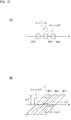
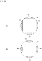
- Fig. 10 is a diagram illustrating a region of the frequency space used for component separation according to the third embodiment.
- the opening of the mask 15 may have any shape other than the circular shape. Ranges of the region AR1a of the Oth-order component, the region AR1b of the +lst-order component, and the region AR1c of the -1st-order component can be obtained by numerical simulation, theoretical calculation, and the like in both of a case in which the opening of the mask 15 has a circular shape and a case in which the opening of the mask 15 has a shape other than a circular shape.
- Fig. 10(A) illustrates the respective regions on a k xs -k ys plane.
- Each of the region AR1a of the Oth-order component, the region AR1b of the +lst-order component, and the region AR1c of the -1st-order component is a circular region. Diameters of the region AR1a of the Oth-order component, the region AR1b of the +lst-order component, and the region AR1c of the -1st-order component are the same.
- the diameter of the region AR1a of the Oth-order component is 4 ⁇ k NA ex .
- the region AR1a of the Oth-order component is a region centered on an origin.
- Each of the region AR1b of the +1st-order component and the region AR1c of the -1st-order component is a region the center of which is disposed on an axis of k xs .
- a distance A between the center of the region AR1c of the -1st-order component and the origin is 2(1 - ⁇ )k NA ex .
- the region AR1b of the +lst-order component is a region at a position symmetrical to the region AR1c of the -1st-order component with respect to the region AR1a of the Oth-order component.
- Fig. 10(B) illustrates the respective regions on a k xs -kx plane.
- Each of the region AR1a of the 0th-order component, the region AR1b of the +lst-order component, and the region AR1c of the -1st-order component is a parallelogram region.
- the image processor 7 sets the region of the frequency space for component separation on the basis of light intensity distribution of the excitation light on the sample S. For example, the image processor 7 sets a plurality of regions that do not overlap each other on the basis of the electric field intensity ill(r) of the excitation light on the sample plane Sa as the light intensity distribution of the excitation light on the sample S.
- the regions described above include three or more regions that do not overlap each other.
- the regions described above include the region AR1a in Fig. 10 as a first region, the region AR1b in Fig. 10 as a second region, and the region AR1c in Fig. 10 as a third region.
- the image processor 7 performs component separation by extracting each of data belonging to the first region (region AR1a), data belonging to the second region (region AR1b), and data belonging to the third region (region AR1c) from the data in the frequency space.
- the image processor 7 calculates image data in a real space by performing four-dimensional inverse Fourier transformation on each of I 0 ⁇ (k,k s ), I +1 ⁇ (k,k s ), and I -1 ⁇ (k,k s ).
- image data obtained by performing inverse Fourier transformation on I 0 ⁇ (k,k s ) is represented as I 0 (r,r s ).
- Image data obtained by performing inverse Fourier transformation on I +1 ⁇ (k,k s ) is represented as I +1 (r,r s ).
- Image data obtained by performing inverse Fourier transformation on I -1 ⁇ (k,k s ) is represented as I -1 (r,r s ).
- the image processor 7 performs an arithmetic operation represented by the following expression (16) on each of I 0 (r,r s ), I +1 (r,r s ), and I -1 (r,r s ).
- ⁇ (r) represents a phase shift amount for each position r of the detector 6a of the detection device 6.
- the image processor 7 calculates a sum of arithmetic results of the three expressions in the expression (16) described above as represented by the following expression (17).
- I ′ r r s I ′ 0 r r s + I ′ + 1 r r s + I ′ ⁇ 1 r r s
- I'(r,r s ) obtained by the arithmetic operation of the expression (17) described above is an image in which distortion of the shape of the effective PSF for each position r of the detector 6a is corrected and the shapes of the effective PSFs are substantially the same.
- the image processor 7 corrects the positional deviation of the effective PSF for each detector 6a of the detection device 6 for I'(r,r s ). Due to this, the effective PSFs of two or more detectors 6a of the detection device 6 can be caused to be substantially the same.
- the image processor 7 generates an image by adding up the images of the respective detectors 6a the effective PSFs of which are corrected to be substantially the same.
- the following describes a method of determining the region in which component separation is performed, a method of determining the phase shift amount for phase shift processing, a method of correcting the positional deviation of the effective PSF, and a super resolution effect obtained through the present method.
- F r,rs represents Fourier transformation of r and r s .
- OTF det represents Fourier transformation of PSF det and represents the OTF of the detection optical system 5.
- ill ⁇ represents Fourier transformation of ill, OTF ill represents Fourier transformation of PSF ill , and
- Obj ⁇ represents Fourier transformation of Obj.
- the expression (18) is a sum of three terms as represented by the following expression (19).
- I ⁇ k k s I 0 ⁇ k k s + I + 1 ⁇ k k s + I ⁇ 1 ⁇ k k s
- I 0 ⁇ (k,k s ) of the first term on the right side of the expression (19) is referred to as the 0th-order component
- I +1 ⁇ (k,k s ) of the second term on the right side is referred to as the +lst-order component
- I -1 ⁇ (k,k s ) of the third term on the right side is referred to as the - 1st-order component.
- the cutoff frequency of OTF det (k) is given as 2k NA em .
- the cutoff frequency of OTF ill (k) is given as 2 ⁇ k NA ex .
- OTF det (k) has a value only in a range in which
- OTF ill (k-k s ) has a value only in a range in which
- OTF ill (k-k s -k 0 ) has a value only in a range in which
- OTF ill (k-k s +k 0 ) has a value only in a range in which
- each value of the regions represented by the respective expressions (13) to (15) may be extracted.
- Each of the region AR1a of the Oth-order component, the region AR1b of the +lst-order component, and the region AR1c of the -1st-order component may be larger or smaller than the region represented by each of the expressions (13) to (15).
- the region in which component separation is performed can be determined by calculating a region in which OTF det and OTF ill have values by theoretical calculation, simulation, and the like.
- I 0 ⁇ (k,k s ), I +1 ⁇ (k,k s ), and I -1 ⁇ (k,k s ) that are returned to the real space by inverse Fourier transformation are respectively assumed to be I 0 (r,r s ), I +1 (r,r s ), and I -1 (r,r s ).
- the image processor 7 performs the processing represented by the expression (16) and the expression (17) described above on results of component separation and inverse Fourier transformation. In this way, the phase of the interference fringes L2 is shifted in accordance with the detector coordinates r.
- the shift amount of the phase of the interference fringes is determined so that a peak position of a function obtained as a product of PSF det (r+r s ) and PSF ill (r s ) and the peak of the interference fringes substantially match each other, for example.
- the deviation amount of the phase of the interference fringes is determined as follows, for example.
- the image processor 7 calculates a positional deviation amount of a signal detected at the detector coordinates r.
- the image processor 7 calculates the positional deviation amount described above by obtaining the peak position of the function obtained as a product of PSF det (r+r s ) and PSF ill (r s ).
- the positional deviation of the effective PSF can be considered to be proportional to the detector coordinates r.
- a parameter representing a degree of deviation is assumed to be ⁇ , and the positional deviation amount is represented as r/ ⁇ .
- a value of ⁇ may be calculated from the peak position of the function obtained as a product of PSF det (r+r s ) and PSF ill (r s ) or may be calculated by numerical simulation.
- ⁇ the phase shift amount corresponding to the detector coordinates is determined.
- the phase shift amount ⁇ (r) of the interference fringes L2 is determined so that the peak position of the function obtained as a product of PSF det (r+r s ) and PSF ill (r s ) matches the peak position of the interference fringes.
- a value of an initial phase ⁇ may be a value that is measured in advance by using fluorescent beads or may be a value estimated from an observation image.
- the image processor 7 determines a conversion amount of the phase (phase shift amount) on the basis of the light intensity distribution of the excitation light on the sample S.
- the image processor 7 determines the phase shift amount on the basis of the electric field intensity ill(r) of the excitation light on the sample plane Sa as the light intensity distribution of the excitation light on the sample S.
- the image processor 7 After performing the phase shift processing as described above, the image processor 7 performs processing of correcting the positional deviation of the effective PSF for each detector 6a. When the processing of correcting the positional deviation is performed, the effective PSFs of the images of the respective detectors 6a of the detection device 6 become substantially the same.
- the image processor 7 generates the super resolution image I SR (r s ) by adding up the images of the respective detectors 6a of the detection device 6. This series of processing is represented by the following expression (22).
- I SR r s ⁇ ⁇ ⁇ PH r I ′ r , r s ⁇ r ⁇ d r
- PH(r) represents a pinhole function defined by the following expression (23).
- PH r ⁇ 1 , x 2 + y 2 ⁇ r PH 2 0 , x 2 + y 2 > r PH 2
- PSF SR (r s ) as the effective PSF of the image obtained by the arithmetic operation of the expression (22) described above is represented by the following expression (24).
- the full width at half maximum of the PSF eff becomes narrower and the resolving power is improved as the period of the interference fringes L2 is smaller on the basis of the expression (24). That is, as the number of fringes (bright parts) included in the periodic direction of the interference fringes L2 according to the embodiment is increased, the full width at half maximum of the PSF eff is reduced and the resolving power is improved.
- the full width at half maximum of a conventional fluorescence microscope is given as 0.51 ⁇ em /NA.
- the full width at half maximum of the PSF becomes 1.4 times narrower and the resolving power is improved as compared with the conventional fluorescence microscope.
- the full width at half maximum of the PSF of the confocal microscope is preferably 1.5 times or more narrower as compared with the conventional fluorescence microscope. That is, the number of bright parts included in the periodic direction of the interference fringes L2 according to the embodiment is preferably equal to or larger than 3. The same applies to the other embodiments.
- a scanning interval and the interval between the detectors 6a of the detection device 6 may be set on the basis of the cutoff frequency and Nyquist's theorem.
- the scanning interval may be set to be equal to or smaller than ⁇ ex /8NA in the periodic direction of the interference fringes.
- the scanning interval may also be set to be equal to or smaller than ⁇ ex /4NA in a direction perpendicular to the periodic direction of the interference fringes.
- the interval between the detectors 6a of the detection device 6 may be set to be equal to or smaller than ⁇ em /4NA.
- Fig. 11 is a flowchart illustrating the observation method according to the third embodiment.
- the processing from Step S1 to Step S4 is the same as that in Fig. 6 , so that description thereof is omitted.
- the image processor 7 performs Fourier transformation on at least some of the detection results of the detectors 6a.
- the image processor 7 performs four-dimensional Fourier transformation on I(r,r s ).
- the image processor 7 performs component separation in the frequency space.
- the image processor 7 separates the component of the frequency space obtained by Fourier transformation for each region of the frequency space.
- the image processor 7 performs inverse Fourier transformation on the separated component.
- the image processor 7 performs phase shift processing.
- Step S25 the image processor 7 corrects the positional deviation of the effective PSF.
- Step S26 the image processor 7 generates an image (for example, a super resolution image) by adding up the images that are obtained by correcting the positional deviation in Step S25.
- the image processor 7 generates the image by converting the phase of at least part of the data obtained through the component separation.
- the image processor 7 performs phase shift processing on the data in the real space. That is, the image processor 7 uses, as the data obtained through the component separation, data (data in the real space) that is obtained by converting the data subjected to component separation (data in the frequency space) into the data in the real space by inverse Fourier transformation.
- the image processor 7 may perform, in the frequency space, phase shift processing on the data in the frequency space subjected to component separation.
- the image processor 7 (refer to Fig. 4 ) performs component separation described in the third embodiment and performs deconvolution on the separated component thereafter to generate an image.
- OTF 0 (k,k s ), OTF +1 (k,k s ), and OTF -1 (k,k s ) are represented by the following expression (26) .
- the image processor 7 performs deconvolution using an estimated value of each of OTF 0 (k,k s ), OTF +1 (k,k s ), and OTF -1 (k,k s ).
- deconvolution for the expression (25) described above using the Wiener filter is represented by the following expression (27).
- A(k s ) is an apodization function for suppressing a negative value of the image.
- w is a Wiener parameter for suppressing noise.
- F ks -1 is inverse Fourier transformation of k s .
- the image processor 7 generates the image using a result of deconvolution described above.
- Fig. 12 is a flowchart illustrating the observation method according to the fourth embodiment.
- the processing from Step S1 to Step S4 is the same as that in Fig. 6 , so that description thereof is omitted.
- the image processor 7 performs Fourier transformation on the detection result.
- the image processor 7 separates the component in the frequency space.
- the image processor 7 performs deconvolution using the component separated through the processing in Step S32.
- the image processor 7 performs apodization.
- Step S35 the image processor 7 performs inverse Fourier transformation on data obtained through deconvolution and apodization.
- the image processor 7 generates the image using data obtained through inverse Fourier transformation.
- the image processor 7 performs component separation, deconvolution, and apodization in the frequency space, and converts the data obtained through these pieces of processing into data in the real space to generate the image.
- the image processor 7 may generate the image without performing processing of causing the effective PSFs of the respective detectors 6a of the detection device 6 to substantially match each other to correct a positional deviation.
- the scanning interval and the interval between the detectors 6a of the detection device 6 may be set on the basis of the cutoff frequency and Nyquist's theorem.
- the scanning interval may be set to be equal to or smaller than ⁇ ex /8NA in the periodic direction of the interference fringes.
- the scanning interval may be set to be equal to or smaller than ⁇ ex /4NA in a direction perpendicular to the periodic direction of the interference fringes.
- the interval between the detectors 6a of the detection device 6 may be set to be equal to or smaller than ⁇ em /4NA.
- the image processor 7 may set a range of k as an addition target to be a range of the entire space, or to be a partial range of the entire space.
- the image processor 7 may limit a range of r at the time of performing arithmetic operation on I 0 ⁇ (k,k s ), I +1 ⁇ (k,k s ), and I -1 ⁇ (k,k s ) by Fourier transformation.
- the image processor 7 may use, as OTF 0 (k,k s ), OTF +1 (k,k s ), and OTF -1 (k,k s ), data that is obtained in advance by measurement using fluorescent beads, numerical simulation using a design value, or the like, or data (for example, an estimated value) that is obtained from a result obtained by detecting fluorescence from the sample S by the detection device 6.
- Fig. 13 is a diagram illustrating the microscope according to the fifth embodiment.
- the detection device 6 includes a line sensor (line detector) in which the detectors 6a are one-dimensionally arranged.
- the detectors 6a are arranged in one direction in the detection device 6.
- the detection device 6 is disposed at a position that is optically conjugate to the sample plane Sa.
- the direction in which the detectors 6a are arranged (hereinafter, referred to as an arrangement direction) is set to be a direction corresponding to the periodic direction of the interference fringes L2.
- the periodic direction of the interference fringes is the X-direction
- the arrangement direction of the detectors 6a is set to be the Xb-direction corresponding to the X-direction.
- the microscope 1 includes a ⁇ /2 wave plate 30 and an optical path rotator 31 that causes the optical path to rotate about the optical axis.
- the ⁇ /2 wave plate 30 causes polarized light passing through the optical path rotator 31 to rotate on the basis of a rotation angle of the optical path rotated by the optical path rotator 31.
- the optical path rotator 31 is disposed on the optical path between the mask 15 and the sample S in the illumination optical system 4.
- the optical path rotator 31 is, for example, disposed at a position at which the excitation light L1 becomes substantially parallel light on the optical path in the illumination optical system 4.
- the optical path rotator 31 is, for example, disposed at a position through which the excitation light L1 passes in the illumination optical system 4 and the fluorescence L3 passes in the detection optical system 5.
- the optical path rotator 31 is, for example, disposed on the optical path between the dichroic mirror 16 and the sample S.
- the ⁇ /2 wave plate 30 may be disposed on the same side as the sample S with respect to the optical path rotator 31, or may be disposed on the opposite side of the sample S (for example, on the same side as the light source of the excitation light) with respect to the optical path rotator 31.
- the optical path rotator 31 is, for example, an image rotator such as a Dove prism.
- the optical path rotator 31 is disposed to be able to rotate about the optical axis of the illumination optical system 4.
- the optical path rotator 31 is driven by a driver 32 to rotate.
- the Dove prism as the optical path rotator 31, when the Dove prism is rotated about the optical axis of the illumination optical system 4 by ⁇ °, the optical path on a light emitting side of the Dove prism (on the sample S side) is rotated about the optical axis of the illumination optical system 4 by 2 ⁇ ° with respect to the optical path on a light incident side of the Dove prism (on the light source 3 side).
- the incident plane of the excitation light L1 for the sample S is rotated about the Z-direction by 2 ⁇ °
- the periodic direction of the interference fringes L2 is rotated about the Z-direction by 2 ⁇ °.
- the driver 32 causes the optical path rotator 31 to rotate about the optical axis of the illumination optical system 4 by 45°.
- the optical path rotator 31 is included in the fringe direction changer that changes the direction of the interference fringes with respect to the sample.
- the ⁇ /2 wave plate 30 is disposed to be able to rotate about the optical axis of the illumination optical system 4.
- the ⁇ /2 wave plate 30 rotates interlocking with the optical path rotator 31.
- the ⁇ /2 wave plate 30 rotates by an angle that is defined on the basis of a rotation angle of the optical path rotator 31.
- the ⁇ /2 wave plate 30 is fixed to (for example, integrated with) the optical path rotator 31, and rotates together with the optical path rotator 31. In this case, the ⁇ /2 wave plate 30 rotates by the same angle as the rotation angle of the optical path rotator 31.
- the polarization direction of the excitation light L1 is rotated about the optical axis of the illumination optical system 4 by 2 ⁇ ° with respect to the polarization direction on the light incident side (light source 3 side). Due to this, the polarization state of the excitation light L1 at the time of being incident on the sample S becomes S-polarization.
- the optical path rotator 31 in Fig. 13 is also included in an image rotator.
- the image rotator causes an image of the sample S (for example, an image of fluorescence from the sample S) to rotate about the optical axis of the detection optical system 5 with respect to the detectors 6a. That is, the fringe direction changer and the image rotator include the optical path rotator 31 as the same member (optical member).
- the optical path rotator 31 is disposed at a position on which fluorescence is incident on the optical path of the illumination optical system 4.
- the image rotator causes the image of fluorescence to rotate with the optical path rotator 31.
- the optical path rotator 31 adjusts the periodic direction of the interference fringes L2 with respect to the arrangement direction of the detectors 6a of the detection device 6.
- the Dove prism As the optical path rotator 31, when the Dove prism is rotated about the optical axis of the illumination optical system 4 by ⁇ °, the periodic direction of the interference fringes L2 is rotated about the Z-direction by 2 ⁇ °. The optical path of the fluorescence L3 from the sample S is then rotated by - 2 ⁇ ° on the light emitting side (detection device 6 side) with respect to the light incident side (sample S side) of the Dove prism.
- the optical path of light traveling toward the sample S via the Dove prism is rotated, and the periodic direction of the interference fringes L2 with respect to the sample S is changed.
- the optical path of the light traveling from the sample S toward the detection device 6 via the Dove prism is rotated in the opposite direction of the optical path of the light traveling toward the sample S by the same angle.
- the direction in which the detectors 6a are arranged always matches the periodic direction of the interference fringes even in a case in which the periodic direction of the interference fringes is changed by the Dove prism.
- the detection device 6 can detect the fluorescence L3 before and after the periodic direction of the interference fringes L2 is changed.
- the image processor 7 generates the image through the processing described in the first embodiment to the fourth embodiment on the basis of the detection result of the detection device 6.
- the driver 22 causes the mask 15 to rotate to change the periodic direction of the interference fringes L2, but the periodic direction of the interference fringes L2 may be changed by the optical path rotator 31 (for example, the Dove prism) described above.
- the fringe direction changer that changes the periodic direction of the interference fringes L2 may have a form different from both of the driver 22 and the optical path rotator 31.
- the stage 2 may be disposed to be able to rotate about the Z-direction, and the direction of the interference fringes L2 with respect to the sample S may be changed by rotation of the stage 2.
- the stage 2 is included in the fringe direction changer that changes the direction of the interference fringes L2 with respect to the sample S.
- the microscope 1 illustrated in Fig. 14 is different from that in Fig. 13 in the position at which the optical path rotator 31 is disposed.
- the fringe direction changer is the same as that in the first embodiment and includes the mask 15 and the driver 22.
- the optical path rotator 31 serves as both of the fringe direction changer and the image rotator in Fig. 13 but is disposed separately from the fringe direction changer in Fig. 14 .
- the optical path rotator 31 is disposed at a position not overlapping with the optical path of the illumination optical system 4 on the optical path of the detection optical system 5.
- the optical path rotator 31 is disposed at a position on which the excitation light L1 is not incident but the fluorescence L3 is incident.
- the optical path rotator 31 is disposed on the optical path between the dichroic mirror 16 and the detection device 6.
- the periodic direction of the interference fringes L2 is changed when the driver 22 causes the mask 15 and the polarizer 14 to rotate.
- the driver 32 causes the optical path rotator 31 to rotate by an angle that is defined on the basis of rotation angles of the mask 15 and the polarizer 14.
- the driver 32 causes the optical path rotator 31 to rotate to cause a direction of an image projected on the detection device 6 to match the direction in which the detectors 6a are arranged.
- Fig. 15 is a diagram illustrating the microscope according to the sixth embodiment.
- the microscope 1 includes a light shielding member 33.
- the light shielding member 33 is disposed at a position that is optically conjugate to the sample plane Sa or in the vicinity thereof.
- the detection device 6 is disposed at a position that is optically conjugate to the sample plane Sa, and the light shielding member 33 is disposed in the vicinity of the detection device 6.
- the light shielding member 33 may be disposed at a position that is conjugate to the sample plane Sa or in the vicinity thereof.
- the light shielding member 33 has an opening 33a through which the fluorescence L3 passes and blocks the fluorescence L3 around the opening 33a.
- the opening 33a extends in the arrangement direction (Xb-direction) of the detectors 6a in the detection device 6.
- the opening 33a is, for example, a slit having a rectangular shape.
- the light shielding member 33 is disposed so that a long side of the opening 33a becomes substantially parallel with the arrangement direction of the detectors 6a.
- One or both of dimensions and a shape of the opening 33a of the light shielding member 33 may be variable.
- the light shielding member 33 may be a mechanical diaphragm that can change a light shielding region, a spatial light modulator (SLM), or the like.
- SLM spatial light modulator
- One or both of the dimensions and the shape of the opening 33a may be fixed.
- the detection device 6 detects the fluorescence L3 passed through the opening 33a of the light shielding member 33.
- the image processor 7 generates an image on the basis of a detection result of the detection device 6.
- the image processor 7 may perform any of the pieces of processing described in the first embodiment to the fourth embodiment. Herein, the following describes a case in which the phase of the PSFs of the interference fringes L2 is shifted through image processing.
- image data I(x,r s ) corresponding to the detection result of the detection device 6 is represented by the following expression (28).
- I(x,r s ) is three-dimensional data having detector coordinates x corresponding to the position of the detector 6a in the detection device 6 and the scan coordinates (x s ,y s ) as independent variables.
- PH y (y s ) represents a pinhole function representing influence of the light shielding member 33.
- D y is a half of the width of the opening 33a of the light shielding member 33 in the Yb-direction (refer to Fig. 17 ). That is, the width of the opening 33a of the light shielding member 33 in the Yb-direction (refer to Fig. 17 ) is assumed to be 2D y .
- the width in the Yb-direction of the optical path of the fluorescence L3 at the time of being incident on the detector 6a corresponds to the dimension in the Yb-direction of the detector 6a, and a half value of the dimension in the Yb-direction of the detector 6a may be used as a value of D y .
- an illumination shape is assumed to be represented by the expression (2) described above, and the periodic direction of the interference fringes L2 is assumed to be the X-direction.
- ill ⁇ (k x -k xs , k y -k ys ) in the expression (30) is represented by the following expression (31).
- ⁇ represents the initial phase of the interference fringes L2.
- I ⁇ (k x ,k xs ,k ys ) is represented by the following expression (32).
- I ⁇ 0 (k x ,k xs ,k ys ) corresponds to the Oth-order component described in the third embodiment
- I ⁇ +1 (k x ,k xs ,k ys ) corresponds to the +lst-order component
- I ⁇ -1 (k x ,k xs ,k ys ) corresponds to the -1st-order component.
- Regions in which I ⁇ 0 (k x ,k xs ,k ys ), I ⁇ +1 (k x ,k xs ,k ys ), and I ⁇ -1 (k x ,k xs ,k ys ) have respective values are different from each other.
- Fig. 16 is a diagram illustrating a region of the frequency space used for component separation according to the sixth embodiment. Ranges in the k ys -direction of the regions in which the Oth-order component, the +lst-order component, and the -1st-order component have respective values depend on PH y ⁇ and OTF det . Fig. 16 illustrates the regions in which the components have respective values in a case in which the opening 15a and the opening 15b of the mask 15 (refer to Fig. 2 ) have a circular shape.
- the opening of the mask 15 has a shape other than the circular shape
- analytic calculation, numerical simulation, or the like may be performed.
- each of the region AR1a of the Oth-order component, the region AR1b of the +lst-order component, and the region AR1c of the -1st-order component is a region having an elliptic shape on the k xs -k ys plane.
- the region AR1a of the Oth-order component, the region AR1b of the +lst-order component, and the region AR1c of the -1st-order component have the same width in the k xs -direction on the k xs -k ys plane.
- the width of the region AR1a of the 0th-order component is 4 ⁇ k NA ex .
- the region AR1a of the 0th-order component is a region centered on an origin.
- Each of the region AR1b of the +lst-order component and the region AR1c of the -1st-order component is a region having the center on the axis of k xs .
- a distance between the center of the region AR1c of the -1st-order component and the origin is 2(1 - ⁇ )k NA ex .
- the region AR1c of the +lst-order component is a region at a position symmetrical to the region AR1c of the -1st-order component with respect to the region AR1a of the Oth-order component.
- the image processor 7 extracts each component from I ⁇ (k x ,k xs ,k ys ). For example, the image processor 7 extracts data of the region AR1a of the Oth-order component from I ⁇ (k x ,k xs ,k ys ) to separate I 0 ⁇ (k x ,k xs ,k ys ) therefrom. The image processor 7 extracts data of the region AR1b of the +lst-order component from I ⁇ (k x ,k xs ,k ys ) to separate I +1 ⁇ (k x ,k xs ,k ys ) therefrom.
- the image processor 7 extracts data of the region AR1c of the -1st-order component from I ⁇ (k x ,k xs ,k ys ) to separate I -1 ⁇ (k x ,k xs ,k ys ) therefrom.
- the image processor 7 performs inverse Fourier transformation on each of I 0 ⁇ (k x ,k xs ,k ys ), I +1 ⁇ (k x ,k xs ,k ys ), and I -1 ⁇ (k x ,k xs ,k ys ) that are obtained through component separation, and calculates data of each component in the real space.
- the data obtained by performing inverse Fourier transformation on I 0 ⁇ (k x ,k xs ,k ys ) is represented as I 0 (x,x s ,y s )
- data obtained by performing inverse Fourier transformation on I +1 ⁇ (k x ,k xs ,k ys ) is represented as I +1 (x,x s ,y s )
- data obtained by performing inverse Fourier transformation on I -1 ⁇ (k x ,k xs ,k ys ) is represented as I -1 (x,x s ,y s ).
- the image processor 7 shifts the phase of the interference fringes in accordance with the detector coordinates so that the effective PSFs of the respective detectors 6a of the detection device 6 are aligned by using at least part of the data of the respective components in the real space obtained as described above.
- the image processor 7 shifts the phase of the interference fringes L2 by arithmetic operations represented by the following expressions (33) and (34).
- the image processor 7 performs correction processing of collecting the positional deviation. After the correction processing, the image processor 7 generates a super resolution image by adding up images of the respective detectors.
- Fig. 17 is a diagram illustrating the microscope according to the seventh embodiment.
- the microscope 1 includes the driver 22 and a driver 34.
- the driver 22 is the same as that in the first embodiment.
- the driver 22 causes the mask 15 to rotate to change the periodic direction of the interference fringes L2.
- the driver 22 is included in the fringe direction changer that changes the direction of the interference fringes L2 with respect to the sample S.
- the detection device 6 can rotate about the Zb-direction.
- the driver 34 causes the detection device 6 to rotate about the Zb-direction.
- the driver 34 causes the detection device 6 to rotate so that the arrangement direction of the detectors 6a in the detection device 6 corresponds to the periodic direction of the interference fringes L2.
- the driver 22 causes the mask 15 to rotate by 90°
- the periodic direction of the interference fringes L2 is changed by 90°, so that the driver 34 causes the detection device 6 to rotate by 90°.
- the driver 34 causes the light shielding member 33 to rotate so that relative positions of the detection device 6 and the light shielding member 33 are maintained.
- the light shielding member 33 is integrated with the detection device 6, and the driver 34 causes the light shielding member 33 and the detection device 6 to integrally rotate.
- the microscope 1 may include the optical path rotator 31 illustrated in Fig. 14 instead of causing the detection device 6 to rotate.
- the microscope 1 does not necessarily include the light shielding member 33 as illustrated in Fig. 13 .
- Fig. 18 is a diagram illustrating the microscope according to the eighth embodiment.
- the illumination pupil is divided into two poles (two regions) on the pupil plane P0 (refer to Fig. 2(C) ), but the illumination pupil may have another form.
- the following describes a form in which the illumination pupil is divided into four poles (four regions) on the pupil plane.
- the illumination optical system 4 includes the collimator lens 12, a ⁇ /2 wave plate 35, a polarized light separating element 36, a mirror 37, a mask 38 (opening member), a mirror 39, a mask 40 (opening member), and a polarized light separating element 41 on the light emitting side of the optical fiber 11.
- the configuration from the dichroic mirror 16 to the objective lens 21 of the illumination optical system 4 is the same as that in the first embodiment.
- the excitation light L1 emitted from the optical fiber 11 is converted into substantially parallel light by the collimator lens 12 and is incident on the ⁇ /2 wave plate 35.
- the excitation light L1 passed through the ⁇ /2 wave plate 35 includes excitation light L1c as linearly polarized light in a first direction and excitation light L1d as linearly polarized light in a second direction.
- a direction of an optical axis (a fast axis, a slow axis) of the ⁇ /2 wave plate 35 is set so that a ratio between an amount of the excitation light L1c and an amount of the excitation light L1d becomes a predetermined ratio.
- the excitation light L1 (the excitation light L1c and the excitation light L1d) passed through the ⁇ /2 wave plate 35 is incident on the polarized light separating element 36.
- the polarized light separating element 36 includes a polarized light separation film 36a that is inclined with respect to the optical axis 12a of the collimator lens 12.
- the polarized light separation film 36a has a characteristic of reflecting the linearly polarized light in the first direction and transmitting the linearly polarized light in the second direction.
- the polarized light separating element 36 is, for example, a polarized beam splitter prism (PBS prism).
- the linearly polarized light in the first direction described above is S-polarized light with respect to the polarized light separation film 36a.
- the linearly polarized light in the second direction described above is P-polarized light with respect to the polarized light separation film 36a.
- the excitation light L1c as S-polarized light with respect to the polarized light separation film 36a is reflected by the polarized light separation film 36a and is incident on the mask 38 via the mirror 37.
- the excitation light L1d as P-polarized light with respect to the polarized light separation film 36a is transmitted through the polarized light separation film 36a and is incident on the mask 40 via the mirror 39.
- Each of the mask 38 and the mask 40 is a light flux splitter that splits the excitation light that excites a fluorescent substance into a plurality of light fluxes. The mask 38 and the mask 40 will be described later with reference to Fig. 19 .
- the polarized light separating element 41 includes a polarized light separation film 41a that is inclined with respect to the optical path of the excitation light L1c and the optical path of the excitation light L1d.
- the polarized light separation film 41a has a characteristic of reflecting the linearly polarized light in the first direction and transmitting the linearly polarized light in the second direction.
- the polarized light separating element 41 is, for example, a polarized beam splitter prism (PBS prism).
- the linearly polarized light in the first direction described above is S-polarized light with respect to the polarized light separation film 41a.
- the linearly polarized light in the second direction described above is P-polarized light with respect to the polarized light separation film 41a.
- the excitation light L1c is S-polarized light with respect to the polarized light separation film 41a and is reflected by the polarized light separation film 41a to be incident on the dichroic mirror 16.
- the excitation light L1d is P-polarized light with respect to the polarized light separation film 41a and is transmitted through the polarized light separation film 41a to be incident on the dichroic mirror 16.
- One or both of the polarized light separating element 36 and the polarized light separating element 41 are not necessarily the PBS prism.
- One or both of the polarized light separating element 36 and the polarized light separating element 41 may be a photonic crystal and the like having different characteristics of reflection and transmission for TE-polarized light and TM-polarized light.
- Fig. 19 is a diagram illustrating the mask and the polarization state of the excitation light according to the eighth embodiment.
- the Xc-direction, the Yc-direction, and the Zc-direction are directions respectively corresponding to the X-direction, the Y-direction, and the Z-direction on the sample plane Sa (refer to Fig. 18 ).
- the mask 38 has an opening 38a and an opening 38b.
- the mask 38 is disposed on a pupil plane conjugate plane, or within a range distant therefrom by 100 mm or less.
- the opening 38a and the opening 38b are arranged in the Xc-direction.
- Each of the opening 38a and the opening 38b has a circular shape, for example, but may have a shape other than the circular shape.
- the Xd-direction, the Yd-direction, and the Zd-direction are directions respectively corresponding to the X-direction, the Y-direction, and the Z-direction on the sample plane Sa (refer to Fig. 18 ).
- the mask 40 is disposed on the pupil plane conjugate plane, or within a range distant therefrom by 100 mm or less.
- the mask 38 or the mask 40 may be disposed on the pupil plane, or within a range distant therefrom by 100 mm or less.
- the mask 40 has an opening 40a and an opening 40b.
- the opening 40a and the opening 40b are arranged in the Yd-direction.
- Each of the opening 40a and the opening 40b has a circular shape, for example, but may have a shape other than the circular shape.
- the reference numeral AR2a denotes a region on which the excitation light L1c passed through the opening 38a of the mask 38 is incident on the pupil plane P0 of the objective lens 21.
- the reference numeral AR2b denotes a region on which the excitation light L1c passed through the opening 38b of the mask 38 is incident on the pupil plane P0.
- Each of arrows in the region AR2a and the region AR2b indicates a polarization direction of the excitation light L1c that is incident thereon.
- the region AR2a and the region AR2b are arranged in the X-direction.
- Each of the excitation light L1c incident on the region AR2a and the excitation light L1c incident on the region AR2b is linearly polarized light in the Y-direction.
- the excitation light L1c incident on the region AR2a and the excitation light L1c incident on the region AR2b have the same polarization direction and interfere with each other on the sample plane Sa (refer to Fig. 18 ). Due to this interference, the interference fringes the periodic direction of which is the X-direction is formed on the sample plane Sa.
- the incident plane of the excitation light L1c with respect to the sample plane Sa is the XZ-plane, and the excitation light L1c is incident on the sample S as S-polarized light.
- the reference numeral AR2c denotes a region on which the excitation light L1d passed through the opening 40a of the mask 40 is incident on the pupil plane P0.
- the reference numeral AR2d denotes a region on which the excitation light L1d passed through the opening 40b of the mask 40 is incident on the pupil plane P0.
- Each of arrows in the region AR2c and the region AR2d indicates the polarization direction of the excitation light L1d that is incident thereon.
- the region AR2c and the region AR2d are arranged in the Y-direction.
- Each of the excitation light L1d incident on the region AR2c and the excitation light L1d incident on the region AR2d is linearly polarized light in the X-direction.
- the excitation light L1d incident on the region AR2c and the excitation light L1d incident on the region AR2d have the same polarization direction and interfere with each other on the sample plane Sa (refer to Fig. 18 ). Due to this interference, the interference fringes the periodic direction of which is the Y-direction is formed on the sample plane Sa.
- the incident plane of the excitation light L1d with respect to the sample plane Sa is the YZ-plane, and the excitation light L1c is incident on the sample S as S-polarized light.
- the interference fringes L2 are formed on the sample plane Sa by combining the interference fringes generated by interference of the excitation light L1c and the interference fringes generated by interference of the excitation light L1d.
- Polarization directions of the excitation light L1c and the excitation light L1d are substantially orthogonal to each other, so that interference between the excitation light L1c and the excitation light L1d is suppressed.
- the detection device 6 detects the fluorescence L3 from the sample S via the detection optical system 5.
- the detection device 6 is an image sensor in which the detectors 6a are arranged in two directions, that is, the Xb-direction and the Yb-direction.
- the image processor 7 generates an image on the basis of a detection result of the detection device 6.
- the following describes a case of shifting the phase of the PSFs of the interference fringes L2 through image processing.
- Fig. 20 is a diagram illustrating the pupil conjugate plane and the region of the frequency space used for component separation according to the eighth embodiment.
- the pupil conjugate plane P1 is represented in a wave coordinate space.
- k NA ex (a circle drawn by a dotted line) illustrated in Fig. 20(A) represents a pupil radius of the objective lens 21.
- Each of the region AR2a and the region AR2b on which the excitation light L1c is incident and the region AR2c and the region AR2d on which the excitation light L1d is incident is assumed to have a circular shape herein, but the shape thereof is not limited to the circular shape.
- a radius of each of the regions from the region ARa to the region ARd is ⁇ k NA ex .
- a distance between the center of each of the regions from the region ARa to the region ARd and the optical axis 21a of the objective lens 21 is (1 - ⁇ )k NA ex .
- a distance between the center of the region AR2a and the center of the region AR2b is 2(1 - ⁇ )k NA ex , for example, but the distance is not limited to this value.
- a distance between the center of the region AR2c and the center of the region AR2d is 2(1 - ⁇ )k NA ex , for example, but the distance is not limited to this value.
- the electric field intensity ill(r) on the sample plane Sa is represented by the following expression (35).
- each of k 0 x and k 0 y is a wave vector of the interference fringes L2.
- Expression (35) ill r PSF ill r 2 + cos 2 ⁇ k 0 x ⁇ r + cos2 ⁇ k 0 y ⁇ r 2
- the illumination pupil has four poles, and the interference fringes the periodic direction of which is the X-direction and the interference fringes the periodic direction of which is the Y-direction are added up.
- the image data I(r,r s ) obtained by the detection device 6 is represented by the following expression (36).
- I r r s PSF det r ⁇ x , y Obj r + r s ill r
- the image processor 7 performs four-dimensional Fourier transformation on r and r s of I(r,r s ) in the expression (36) as represented by the following expression (37) .
- OTF det is Fourier transformation of PSF det , and represents the OTF of the detection optical system 5.
- ill ⁇ represents Fourier transformation of ill.
- OTF ill represents Fourier transformation of PSF ill .
- ⁇ x and ⁇ y represent the initial phase in the X-direction of the interference fringes L2 and the initial phase in the Y-direction of the interference fringes L2, respectively.
- Obj ⁇ represents Fourier transformation of Obj.
- the expression (37) is a sum of five terms as represented by the following expression (38).
- I 0 ⁇ (k,k s ) is referred to as the 0th-order component
- I ⁇ +1,x (k,k s ) is referred to as the +1st-order component in the X-direction
- I ⁇ -1,x (k,k s ) is referred to as the -1st-order component in the X-direction
- I ⁇ +1,y (k,k s ) is referred to as the +lst-order component in the Y-direction
- I ⁇ -1,y (k,k s ) is referred to as the - 1st-order component in the Y-direction.
- the reference numeral AR3a denotes a region in which data of the Oth-order component is present (hereinafter, referred to as a region of the Oth-order component).
- the reference numeral AR3b denotes a region in which data of the +1st-order component in the X-direction is present (hereinafter, referred to as a region of the +lst-order component in the X-direction).
- the reference numeral AR3c denotes a region in which data of the -1st-order component in the X-direction is present (hereinafter, referred to as a region of the -1st-order component in the X-direction).
- the reference numeral AR3d denotes a region in which data of the +lst-order component in the Y-direction is present (hereinafter, referred to as a region of the +lst-order component in the Y-direction).
- the reference numeral AR3e denotes a region in which data of the -1st-order component in the Y-direction is present (hereinafter, referred to as a region of the -1st-order component in the Y-direction).
- the region AR3a of the Oth-order component is represented by the following expression (40).
- Expression (40) k ⁇ k s ⁇ 2 ⁇ k NA ex and k ⁇ 2 k NA em
- the region AR3b of the +lst-order component in the X-direction is represented by the following expression (41).
- Expression (41) k ⁇ k s ⁇ k 0 x ⁇ 2 ⁇ k NA ex and k ⁇ 2 k NA em
- the region AR3c of the -1st-order component in the X-direction is represented by the following expression (42).
- Expression (42) k ⁇ k s + k 0 x ⁇ 2 ⁇ k NA ex and k ⁇ 2 k NA em
- the region AR3d of the +lst-order component in the Y-direction is represented by the following expression (43).
- Expression (43) k ⁇ k s ⁇ k 0 y ⁇ 2 ⁇ k NA ex and k ⁇ 2 k NA em
- the region AR3e of the -1st-order component in the Y-direction is represented by the following expression (44).
- Expression (44) k ⁇ k s + k 0 y ⁇ 2 ⁇ k NA ex and k ⁇ 2 k NA em
- the image processor 7 extracts, by filtering, each component from I ⁇ (k,k s ) that is obtained through Fourier transformation. For example, the image processor 7 extracts data in a region satisfying the expression (40) described above from I ⁇ (k,k s ) as the Oth-order component. The image processor 7 extracts data in a region satisfying the expression (41) described above from I ⁇ (k,k s ) as the +lst-order component in the X-direction. The image processor 7 extracts data in a region satisfying the expression (42) described above from I ⁇ (k,k s ) as the -1st-order component in the X-direction.
- the image processor 7 extracts data in a region satisfying the expression (43) described above from I ⁇ (k,k s ) as the +lst-order component in the Y-direction.
- the image processor 7 extracts data in a region satisfying the expression (44) described above from I ⁇ (k,k s ) as the -1st-order component in the Y-direction.
- the image processor 7 calculates the data of each component in the real space by performing inverse Fourier transformation on each extracted component.
- the Oth-order component in the real space is represented as I 0 (r,r s )
- the +lst-order component in the X-direction in the real space is represented as I +1,x (r,r s )
- the -1st-order component in the X-direction in the real space is represented as I -1,x (r,r s ).
- the +lst-order component in the Y-direction in the real space is represented as I +1,y (r,r s ), and the -1st-order component in the Y-direction in the real space is represented as I -1,y (r,r s ).
- the image processor 7 shifts the phase of the interference fringes in accordance with the detector coordinates so that the effective PSFs of the respective detectors 6a of the detection device 6 are aligned.
- the image processor 7 shifts the phase of each of the +1st-order component in the X-direction, the -1st-order component in the X-direction, the +lst-order component in the Y-direction, and the -1st-order component in the Y-direction in the real space.
- ⁇ x (r) represents the phase shift amount for each of the +lst-order component and the - 1st-order component in the X-direction.
- ⁇ y (r) represents the phase shift amount for each of the +lst-order component and the -1st-order component in the Y-direction.
- the phase shift amount described above is, for example, set so that a peak position of a function obtained as a product of PSF det (r+r s ) and PSF ill (r s ) matches the peak position of the interference fringes L2.
- the image processor 7 adds up the respective components as represented by the following expression (46).
- the image processor 7 performs correction processing of correcting the positional deviation for each of the detectors 6a.
- the image processor 7 then generates a super resolution image by adding up pieces of data subjected to the correction processing.
- the region used for component separation is not limited to the regions represented by the expression (41) to the expression (44) described above.
- the region used for component separation may be larger or smaller than the regions represented by the expression (41) to the expression (44) described above.
- At least one of the opening 38a and the opening 38b of the mask 38 and the opening 40a and the opening 40b of the mask 40 does not necessarily have a circular shape.
- the region used for component separation can be obtained by numerical simulation, theoretical calculation, and the like in both of a case in which the opening of the mask has a circular shape and a case in which the opening of the mask has a shape other than the circular shape.
- the processing performed by the image processor 7 may be any of the pieces of processing described in the first embodiment to the fourth embodiment.
- the three components are used in the expression (27)
- five components including the Oth-order component, the +lst-order component in the X-direction, the -1st-order component in the X-direction, the +lst-order component in the Y-direction, and the -1st-order component in the Y-direction may be used in the present embodiment.
- Fig. 21 is a diagram illustrating the microscope according to the ninth embodiment.
- the microscope 1 includes the ⁇ /2 wave plate 30 and the optical path rotator 31 described above with reference to Fig. 13 .
- the optical path rotator 31 is driven by the driver 32 to rotate about the optical axis of the illumination optical system 4.
- each of the optical path of the excitation light L1c and the optical path of the excitation light L1d rotates about the optical axis of the illumination optical system 4.
- the periodic direction of the interference fringes L2 formed on the sample plane Sa is rotated about the Z-direction.
- Fig. 22 is a diagram illustrating the polarization state of the excitation light according to the ninth embodiment.
- regions AR4a on which the excitation light L1c is incident on the pupil plane P0 are arranged in the X-direction.
- a region AR4b and a region AR4b on which the excitation light L1d is incident on the pupil plane P0 are arranged in the Y-direction.
- Fig. 22(B) corresponds to a state in which the Dove prism (the optical path rotator 31 in Fig. 21 ) and the ⁇ /2 wave plate 30 are rotated by 22.5° from the state in Fig. 22(A) .
- the regions AR4a on which the excitation light L1c is incident on the pupil plane P0 are arranged in a direction rotated from the X-direction by 45°.
- the periodic direction of the interference fringes of the excitation light L1c on the sample plane Sa is a direction rotated from the X-direction by 45°.
- the regions AR4b on which the excitation light L1d is incident on the pupil plane P0 are arranged in a direction rotated from the Y-direction by 45°.
- the periodic direction of the interference fringes of the excitation light L1d on the sample plane Sa is a direction rotated from the Y-direction by 45°.
- the detection device 6 detects the fluorescence L3 from the sample S before and after the periodic direction of the interference fringes L2 is changed.
- the image processor 7 generates an image on the basis of a detection result of the detection device 6 before the periodic direction of the interference fringes L2 is changed and a detection result of the detection device 6 after the periodic direction of the interference fringes L2 is changed.
- the optical path rotator 31 may be disposed on the optical path between the dichroic mirror 16 and the detection device 6.
- the microscope 1 changes the periodic direction of the interference fringes L2 with the optical path rotator 31, but the fringe direction changer that changes the periodic direction of the interference fringes L2 may have an aspect different from that of the optical path rotator 31.
- Fig. 23 is a diagram illustrating the microscope according to the tenth embodiment.
- Fig. 24 is a diagram illustrating the mask according to the tenth embodiment.
- the microscope 1 includes a driver 45 and a driver 46.
- the mask 38 can rotate about the optical axis of the excitation light L1c.
- the mask 38 is driven by the driver 45 to rotate (refer to Fig. 24(A) ).
- the mask 38 is rotated clockwise by 45°.
- the mask 40 can rotate about the optical axis of the excitation light L1d.
- the mask 40 is driven by the driver 46 to rotate (refer to Fig. 24(B) ).
- the driver 46 causes the mask 40 to rotate by the same angle as the angle of rotation of the mask 38 rotated by the driver 45.
- the mask 40 is rotated clockwise by 45°. Due to this, the periodic direction of the interference fringes L2 on the sample plane Sa is rotated about the Z-direction by 45°.
- a ⁇ /2 wave plate 48 is disposed on the optical path between the polarized light separating element 41 and the dichroic mirror 16.
- the ⁇ /2 wave plate 48 is driven by a driver 49 to rotate about the optical axis of the illumination optical system 4.
- the ⁇ /2 wave plate 48 and the driver 49 adjust each of the excitation light L1c and the excitation light L1d to be incident on the sample S as S-polarized light.
- Fig. 25 is a diagram illustrating the microscope according to the eleventh embodiment.
- the microscope 1 includes a relay optical system 47.
- the relay optical system 47 is part of the illumination optical system 4 and is part of the detection optical system 5.
- the relay optical system 47 is disposed on the optical path between the deflecting mirror 18a and the deflecting mirror 18b in the scanning part 18.
- the deflecting mirror 18a is disposed at substantially the same position as that of a first pupil conjugate plane that is optically conjugate to the pupil plane P0 of the objective lens 21.
- the relay optical system 47 is disposed so that a second pupil conjugate plane that is optically conjugate to the first pupil conjugate plane described above is formed between the deflecting mirror 18b and the lens 19.
- the deflecting mirror 18b is disposed at substantially the same position as that of the second pupil conjugate plane described above.
- the scanning part 18 is not limited to the form described above.
- the stage 2 may include a Y-stage that moves in the Y-direction with respect to the objective lens 21, and the scanning part 18 may include the Y-stage in place of the deflecting mirror 18b.
- the scanning part 18 may scan the sample S in the X-direction with the excitation light L1 by the deflecting mirror 18a and scan the sample S in the Y-direction with the excitation light L1 by moving the Y-stage.
- the deflecting mirror 18a may be disposed at substantially the same position as that of the pupil conjugate plane that is optically conjugate to the pupil plane P0 of the objective lens 21.
- the stage 2 may include an X-stage that moves in the X-direction with respect to the objective lens 21, and the scanning part 18 may include the X-stage in place of the deflecting mirror 18a.
- the scanning part 18 may scan the sample S in the X-direction with the excitation light L1 by moving the X-stage described above, and scan the sample S in the Y-direction with the excitation light L1 by the deflecting mirror 18b.
- the deflecting mirror 18b may be disposed at substantially the same position as that of the pupil conjugate plane that is optically conjugate to the pupil plane P0 of the objective lens 21.
- the stage 2 may include the X-stage that moves in the X-direction with respect to the objective lens 21 and the Y-stage that moves in the Y-direction with respect to the objective lens 21, and the scanning part 18 may include the X-stage and the Y-stage described above.
- the scanning part 18 may scan the sample S in the X-direction with the excitation light L1 by moving the X-stage described above, and scan the sample S in the Y-direction with the excitation light L1 by moving the Y-stage described above.
- the scanning direction in which the sample S is scanned with the interference fringes includes two directions, that is, the X-direction and the Y-direction, and the illumination optical system 4 two-dimensionally scans the sample S with the interference fringes.
- the scanning direction in which the sample S is scanned with the interference fringes may include three directions, that is, the X-direction, the Y-direction, and the Z-direction.
- the microscope 1 may perform 2D processing of scanning the sample S in the X-direction and the Y-direction with the interference fringes to acquire a 2D image, and repeat the 2D processing while changing the position in the Z-direction at which the interference fringes are generated to three-dimensionally scan the sample S with the interference fringes.
- the microscope 1 may acquire a plurality of 2D images the positions of which in the Z-direction are different, and generate a 3D image (for example, a Z-stack).
- the illumination optical system 4 may perform scanning in the X-direction and the Y-direction, and scanning in the Z-direction may be performed by moving the stage 2.
- the illumination optical system 4 may three-dimensionally scan the sample S with the interference fringes.
- Fig. 26 and Fig. 27 are diagrams illustrating the illumination pupil according to modifications.
- the illumination pupil has two poles in Fig. 2 , four poles in Fig. 20 , and three poles in Fig. 26(A) .
- Each of the reference numeral AR5a to the reference numeral AR5c denotes a region on which the excitation light is incident on the pupil plane P0.
- formed are first interference fringes of the excitation light incident on the region AR5a and the excitation light incident on the region AR5b, second interference fringes of the excitation light incident on the region AR5b and the excitation light incident on the region AR5c, and third interference fringes of the excitation light incident on the region AR5c and the excitation light incident on the region AR5a.
- the interference fringes are formed by combining the first interference fringes, the second interference fringes, and the third interference fringes described above.
- each of the periodic direction of the first interference fringes, the periodic direction of the second interference fringes, and the periodic direction of the third interference fringes is the periodic direction, and there are three periodic directions, so that the super resolution effect can be obtained in the three directions.
- the illumination pupil may have five or more poles.
- the illumination pupil has a circular shape in Fig. 2 , for example, but may have any other shape.
- the reference numeral AR6 denotes a region on which the excitation light is incident.
- the region AR6 in Fig. 26(B) is a region surrounded by a circle AR6a as part of a circle centered on the optical axis 21a of the objective lens 21 and a straight line AR6b connecting both ends of the circular arc AR6a.
- the region AR6 in Fig. 26(C) is a region surrounded by a circular arc as part of the circle centered on the optical axis 21a of the objective lens 21 and a curved line AR6c symmetrical to the circular arc AR6a.
- resolving power in a direction in which the interference fringes are not formed is improved, and sectioning is also improved as compared with a case of the illumination pupil having a circular shape.
- resolving power in a direction in which the interference fringes are not formed is improved, and sectioning is also improved as compared with a case of the illumination pupil having the shape illustrated in Fig. 26(C) .
- resolving power in a direction in which the interference fringes are formed is improved as compared with a case of the illumination pupil having the shape illustrated in Fig. 26(B) .
- the illumination pupil has a form obtained by causing the illumination pupil having the shape illustrated in Fig. 26(B) to have four poles.
- the illumination pupil has a form obtained by causing the illumination pupil having the shape illustrated in Fig. 26(C) to have four poles.
- the number of a plurality of regions (the number of poles) on which the excitation light is incident is set to be an optional number equal to or larger than 2.
- a shape of one of the regions on which the excitation light is incident on the pupil plane P0 may have a shape different from the shape of the other regions.
- Dimensions of one of the regions on which the excitation light is incident on the pupil plane P0 may be different from dimensions of the other regions.
- the regions on which the excitation light is incident on the pupil plane P0 may be disposed asymmetrical to each other with respect to the optical axis 21a of the objective lens 21.
- the shape, the dimensions, and the arrangement of each pole of the illumination pupil can be implemented by designing the shape, the dimensions, and the arrangement of the opening of the mask 15 illustrated in Fig. 2 , for example.
- the mask 15 may be a mechanical diaphragm that can change a light shielding region, a spatial light modulator (SLM), or the like.
- Fig. 28 is a diagram illustrating the microscope according to a modification.
- the illumination optical system 4 includes a collimator lens 50, a ⁇ /2 wave plate 51, a lens 52, a diffraction grating 53, a lens 54, and the mask 15 in this order from the optical fiber 11 toward the dichroic mirror 16.
- the collimator lens 50 converts the excitation light L1 from the optical fiber 11 into substantially parallel light.
- the ⁇ /2 wave plate 51 adjusts the polarization state of the excitation light L1 at the time of being incident on the sample S.
- the lens 52 concentrates the excitation light L1 to the diffraction grating 53.
- the diffraction grating 53 causes the excitation light L1 to branch into a plurality of light fluxes by diffraction.
- the diffraction grating 53 is a light flux splitter that splits the excitation light that excites a fluorescent substance into a plurality of light fluxes.
- the diffraction grating 53 is disposed at a focal point of the lens 52, or within a range distant from the focal point by 1 mm or less. That is, the diffraction grating 53 is disposed on a plane that is conjugate to the sample plane Sa, or within a range distant therefrom by 1 mm or less.
- the light fluxes described above include Oth-order diffracted light, +lst-order diffracted light, and -1st-order diffracted light.
- the lens 54 converts each of the Oth-order diffracted light, the +lst-order diffracted light, and the -1st-order diffracted light into substantially parallel light.
- the mask 15 is disposed so that the 0th-order diffracted light is blocked, and at least part of the +1-order diffracted light and at least part of the -1st-order diffracted light pass therethrough. In such a form, the amount of the excitation light L1 transmitted through the mask 15 can be increased.
- the diffraction grating 53 may be designed so that the Oth-order diffracted light is not generated. A configuration not including the mask 15 may also be employed.
- Fig. 29 and Fig. 30 are diagrams illustrating the polarization adjuster according to modifications.
- the optical path of the illumination optical system 4 is bent due to a reflection member such as the dichroic mirror 16 illustrated in Fig. 1 , but the illumination optical system 4 is illustrated in Fig. 29 and Fig. 30 while being exploded to cause the optical axis 4a to be a straight line.
- the Z-direction is a direction parallel with the optical axis 4a
- each of the X-direction and the Y-direction is a direction perpendicular to the optical axis 4a.
- the illumination optical system 4 includes a ⁇ /4 wave plate 61, the mask 15, and a ⁇ /4 wave plate 62.
- the excitation light L1 emitted from the optical fiber 11 is linearly polarized light substantially in the X-direction and is incident on the ⁇ /4 wave plate 61.
- a polarizer for example, a polarizing plate having a transmission axis in the X-direction may be disposed on the optical path between the optical fiber 11 and the ⁇ /4 wave plate 61.
- the fast axis of the ⁇ /4 wave plate 61 is set in a direction obtained by rotating the X-direction counterclockwise by 45° when viewed from the +Z side.
- the excitation light L1 passed through the ⁇ /4 wave plate 61 becomes circularly polarized light and is incident on the mask 15.
- the excitation light L1 passed through the opening 15a and the opening 15b of the mask 15 is circularly polarized light and is incident on the ⁇ /4 wave plate 62.
- the fast axis of the ⁇ /4 wave plate 62 is set in a direction obtained by rotating the X-direction clockwise by 45° when viewed from the +Z side.
- the excitation light L1 passed through the ⁇ /4 wave plate 62 becomes linearly polarized light in the X-direction and is emitted to the sample.
- the mask 15 is disposed to be able to rotate about the optical axis 4a.
- the periodic direction of the interference fringes is changed.
- the opening 15a and the opening 15b of the mask 15 are arranged in the Y-direction, and the periodic direction of the interference fringes is the Y-direction.
- the periodic direction of the interference fringes is rotated by 90° to become the X-direction.
- the ⁇ /4 wave plate 62 can rotate about the optical axis 4a.
- the ⁇ /4 wave plate 62 is disposed to rotate by the same angle as that of the mask 15.
- the ⁇ /4 wave plate 62 is integrated with the mask 15 and rotates integrally with the mask 15.
- the ⁇ /4 wave plate 62 rotates by 90° when the mask 15 rotates by 90°, and the fast axis of the ⁇ /4 wave plate 62 becomes parallel with the fast axis of the ⁇ /4 wave plate 61.
- the excitation light L1 passed through the ⁇ /4 wave plate 62 becomes linearly polarized light in the Y-direction.
- the incident plane of the excitation light L1 with respect to the sample plane is parallel with the periodic direction of the interference fringes, and the excitation light L1 at the time of being incident on the sample plane is linearly polarized light perpendicular to the periodic direction of the interference fringes, so that the excitation light L1 is emitted to the sample plane in a state of S-polarized light.
- the ⁇ /4 wave plate 62 is included in the polarization adjuster that adjusts the polarization state of the excitation light at the time of being incident on the sample.
- a polarization adjuster can reduce loss of the amount of the excitation light L1 as compared with the aspect described above with reference to Fig. 1 .
- the illumination optical system 4 includes a polarizer 65, the mask 15, and a ⁇ /2 wave plate 66.
- the excitation light L1 emitted from the optical fiber 11 is linearly polarized light substantially in the X-direction and is incident on the polarizer 65.
- a transmission axis of the polarizer 65 is set in the X-direction.
- the excitation light L1 passed through the polarizer 65 is linearly polarized light in the X-direction and is incident on the mask 15.
- the excitation light L1 passed through the opening 15a and the opening 15b of the mask 15 is linearly polarized light in the X-direction and is incident on the ⁇ /2 wave plate 66.
- the fast axis of the ⁇ /2 wave plate 66 is set in a direction obtained by rotating the X-direction clockwise by 45° when viewed from the +Z side.
- the excitation light L1 passed through the ⁇ /2 wave plate 66 becomes linearly polarized light in the Y-direction and is emitted to the sample.
- the mask 15 is disposed to be able to rotate about the optical axis 4a.
- the periodic direction of the interference fringes is changed.
- the opening 15a and the opening 15b of the mask 15 are arranged in the X-direction, and the periodic direction of the interference fringes is the X-direction.
- the periodic direction of the interference fringes is rotated by 90° to become the Y-direction.
- the ⁇ /2 wave plate 66 can rotate about the optical axis 4a.
- the ⁇ /2 wave plate 66 is disposed to rotate by a half angle of the rotation angle of the mask 15. For example, when the mask 15 rotates by 90°, the ⁇ /2 wave plate 66 rotates by 45°. In this case, the excitation light L1 passed through the ⁇ /2 wave plate 66 becomes linearly polarized light in the X-direction.
- the incident plane of the excitation light L1 with respect to the sample plane is parallel with the periodic direction of the interference fringes, and the excitation light L1 at the time of being incident on the sample plane is linearly polarized light perpendicular to the periodic direction of the interference fringes, so that the excitation light L1 is emitted to the sample plane in a state of S-polarized light.
- the ⁇ /2 wave plate 66 is included in the polarization adjuster that adjusts the polarization state of the excitation light at the time of being incident on the sample.
- Such a polarization adjuster can reduce loss of the amount of the excitation light L1 as compared with the aspect described above with reference to Fig. 1 .
- the detection device 6 may include an image sensor, and include an image rotator that causes an image of the sample S to rotate about the optical axis of the detection optical system 5. In a case of rotating a fringe direction, a fringe period can be caused to match the position of the detector by rotating the image of the sample S.
- the image processor 7 includes a computer system, for example.
- the image processor 7 reads out an image processing program stored in a storage and performs various kinds of processing in accordance with the image processing program.
- the image processing program causes a computer to generate an image on the basis of a detection result of the detection device 6.
- the detection result of the detection device 6 described above is obtained by splitting light from a light source into a plurality of light fluxes, scanning the sample in a plurality of directions with the interference fringes that are generated by interference of at least part of the light fluxes, and detecting light from the sample by a detection device including a plurality of detectors via a detection optical system on which the light from the sample is incident.
- a technical scope of the present invention is not limited to the aspect described above in the embodiments.
- One or more of requirements described above in the embodiments may be omitted.
- the requirements described above in the embodiments can be combined as appropriate. As long as being allowed by the law, all documents cited in the embodiments described above are incorporated herein as part of the description.
Landscapes
- Physics & Mathematics (AREA)
- General Physics & Mathematics (AREA)
- Optics & Photonics (AREA)
- Chemical & Material Sciences (AREA)
- Analytical Chemistry (AREA)
- Engineering & Computer Science (AREA)
- Computer Vision & Pattern Recognition (AREA)
- General Engineering & Computer Science (AREA)
- Microscoopes, Condenser (AREA)
- Investigating, Analyzing Materials By Fluorescence Or Luminescence (AREA)
Abstract
Description
- The present invention relates to a microscope and an observation method.
- There has been developed a scanning type microscope that detects fluorescence from a sample (for example, refer to the following Non-Patent Literature 1).
- [Non-Patent Literature 1] Confocal laser scanning microscopy with spatiotemporal structured illumination, Peng Gao, G. Ulrich Nienhaus, Optics Letters, Vol. 41, No. 6, 1193-1196, 2016.3.15
- A first aspect of the present invention provides a microscope including: an illumination optical system that includes a light flux splitter that splits light from a light source into a plurality of light fluxes, and scans a sample in a plurality of directions with interference fringes that are generated by interference of at least part of the light fluxes split by the light flux splitter; a detection optical system on which light from the sample is incident; a detection device including a plurality of detectors that detect the light from the sample via the detection optical system; and an image processor that generates an image using detection results obtained by two or more detectors of the detection device.
- A second aspect of the present invention provides an observation method including: splitting the light from the light source into a plurality of light fluxes, and scanning the sample in a plurality of directions with the interference fringes that are generated by interference of at least part of the light fluxes; detecting the light from the sample with the detection device including the detectors via the detection optical system on which the light from the sample is incident; and generating an image using detection results obtained by two or more detectors of the detection device.
-
-
Fig. 1 is a diagram illustrating a microscope and an optical path of excitation light according to a first embodiment. -
Fig. 2 is a diagram illustrating a mask and a polarizer according to the first embodiment. -
Fig. 3 is a diagram illustrating a mask, a polarizer, interference fringes, and a polarization state of excitation light according to the first embodiment. -
Fig. 4 is a diagram illustrating the microscope and an optical path of fluorescence according to the first embodiment. -
Fig. 5 is a diagram illustrating an effective PSF at each position of a detection device according to the first embodiment. -
Fig. 6 is a flowchart illustrating an observation method according to the first embodiment. -
Fig. 7 is a diagram illustrating processing performed by an image processor of a microscope according to a second embodiment. -
Fig. 8 is a flowchart illustrating an observation method according to the second embodiment. -
Fig. 9 is a diagram illustrating processing performed by an image processor of a microscope according to a third embodiment. -
Fig. 10 is a diagram illustrating a region of a frequency space used for component separation according to the third embodiment. -
Fig. 11 is a flowchart illustrating an observation method according to the third embodiment. -
Fig. 12 is a flowchart illustrating an observation method according to a fourth embodiment. -
Fig. 13 is a diagram illustrating a microscope according to a fifth embodiment. -
Fig. 14 is a diagram illustrating the microscope according to the fifth embodiment. -
Fig. 15 is a diagram illustrating a microscope according to a sixth embodiment. -
Fig. 16 is a diagram illustrating a region of the frequency space used for component separation according to the sixth embodiment. -
Fig. 17 is a diagram illustrating a microscope according to a seventh embodiment. -
Fig. 18 is a diagram illustrating a microscope according to an eighth embodiment. -
Fig. 19 is a diagram illustrating a mask and a polarization state of excitation light according to the eighth embodiment. -
Fig. 20 is a diagram illustrating interference fringes and a region of the frequency space used for component separation according to the eighth embodiment. -
Fig. 21 is a diagram illustrating a microscope according to a ninth embodiment. -
Fig. 22 is a diagram illustrating a polarization state of excitation light according to the ninth embodiment. -
Fig. 23 is a diagram illustrating a microscope according to a tenth embodiment. -
Fig. 24 is a diagram illustrating a mask according to the tenth embodiment. -
Fig. 25 is a diagram illustrating a microscope according to an eleventh embodiment. -
Fig. 26 is a diagram illustrating an illumination pupil according to a modification. -
Fig. 27 is a diagram illustrating the illumination pupil according to a modification. -
Fig. 28 is a diagram illustrating a microscope according to a modification. -
Fig. 29 is a diagram illustrating a polarization adjuster according to a modification. -
Fig. 30 is a diagram illustrating the polarization adjuster according to a modification. - The following describes a first embodiment.
Fig. 1 is a diagram illustrating a microscope and an optical path of excitation light according to the first embodiment. In the following embodiment, amicroscope 1 is assumed to be a scanning type fluorescence microscope, but the microscope according to the embodiment is not limited to a scanning type microscope or a fluorescence microscope. Themicroscope 1 includes astage 2, alight source 3, an illuminationoptical system 4, a detectionoptical system 5, adetection device 6, and animage processor 7. Themicroscope 1 operates as follows in brief. - The
stage 2 holds a sample S as an observation target. The sample S is a cell and the like subjected to fluorescent staining in advance. The sample S contains a fluorescent substance such as a fluorescent dye. Thelight source 3 emits excitation light L1 that excites the fluorescent substance contained in the sample S. The illuminationoptical system 4 scans the sample S in a plurality of directions (for example, the X-direction and the Y-direction) with interference fringes L2 of the excitation light L1. The illuminationoptical system 4 two-dimensionally scans the sample S with the interference fringes L2. The detectionoptical system 5 is disposed at a position on which fluorescence L3 (illustrated inFig. 4 described later) from the sample S is incident. Thedetection device 6 includes a plurality ofdetectors 6a (illustrated inFig. 4 described later) that detect the fluorescence L3 from the sample S via the detectionoptical system 5. Theimage processor 7 generates an image (for example, a super resolution image) using detection results obtained by two or more of thedetectors 6a of thedetection device 6. The following describes respective parts of themicroscope 1. - The
light source 3 includes, for example, a light source such as a laser element. Thelight source 3 generates coherent light of a predetermined wavelength band. The predetermined wavelength band is set to be a wavelength band including an excitation wavelength of the sample S. The excitation light L1 emitted from thelight source 3 is, for example, linearly polarized light. A light guide member such as anoptical fiber 11 is connected to an emitting port of thelight source 3. Themicroscope 1 does not necessarily include thelight source 3, and thelight source 3 may be provided separately from themicroscope 1. For example, thelight source 3 may be disposed in themicroscope 1 in a replaceable (attachable, or removable) manner. Thelight source 3 may be externally mounted on themicroscope 1 at the time of observation by themicroscope 1. - The illumination
optical system 4 is disposed at a position on which the excitation light L1 from thelight source 3 is incident. The excitation light L1 is incident on the illuminationoptical system 4 from thelight source 3 via theoptical fiber 11. Theoptical fiber 11 may be part of the illuminationoptical system 4 or may be part of a light source device including thelight source 3. The illuminationoptical system 4 includes acollimator lens 12, a λ/4wave plate 13, apolarizer 14, a mask 15 (opening member), adichroic mirror 16, a relayoptical system 17, ascanning part 18, alens 19, alens 20, and anobjective lens 21 in this order from thelight source 3 side toward the sample S side. - In the following description, an XYZ orthogonal coordinate system illustrated in
Fig. 1 , for example, should be referred to as appropriate. In the XYZ orthogonal coordinate system, each of the X-direction and the Y-direction is a direction perpendicular to anoptical axis 21a of theobjective lens 21. The Z-direction is a direction parallel with theoptical axis 21a of theobjective lens 21. Theoptical axis 21a of theobjective lens 21 is included in anoptical axis 4a of the illuminationoptical system 4. For each of the X-direction, the Y-direction, and the Z-direction, the same side as an arrow is referred to as a + side (for example, +X side), and the opposite side of the arrow is referred to as a - side (for example, -X side) as appropriate. In a case in which an optical path is bent by reflection, a direction corresponding to each of the X-direction, the Y-direction, and the Z-direction is represented by adding a subscript. For example, the Xa-direction, the Ya-direction, and the Za-direction inFig. 1 are directions respectively corresponding to the X-direction, the Y-direction, and the Z-direction on the optical path from thecollimator lens 12 to thedichroic mirror 16. - The
collimator lens 12 converts the excitation light L1 emitted from theoptical fiber 11 into parallel light. For example, thecollimator lens 12 is disposed so that a focal point thereof on the same side as thelight source 3 is aligned with a light emitting port of theoptical fiber 11. In the following description, a focal point of the lens included in the illuminationoptical system 4 on the same side as thelight source 3 is referred to as a rear side focal point, and a focal point thereof on the same side as the sample S is referred to as a front side focal point as appropriate. - The λ/4
wave plate 13 causes the polarization state of the excitation light L1 to be circular polarization. Thepolarizer 14 is, for example, a polarizing plate, and has a characteristic of transmitting linearly polarized light in a predetermined direction. Thepolarizer 14 is disposed so that light incident on the sample S becomes S-polarized light (linearly polarized light in the Y-direction). Thepolarizer 14 can rotate about anoptical axis 12a of thecollimator lens 12. Theoptical axis 12a of thecollimator lens 12 is included in theoptical axis 4a of the illuminationoptical system 4. - The
mask 15 is a light flux splitter that splits excitation light that excites a fluorescent substance into a plurality of light fluxes. The illuminationoptical system 4 scans the sample S with the interference fringes L2 that are generated by interference of two or more of the light fluxes split by themask 15. Themask 15 is disposed at a position of a pupil conjugate plane P1 that is optically conjugate to a pupil plane P0 of theobjective lens 21, or within a range distant therefrom by 100 mm or less. Themask 15 may also be disposed on the pupil plane P0, or within a range distant therefrom by 100 mm or less. - The
mask 15 has anopening 15a and anopening 15b through which the excitation light L1 passes. The interference fringes L2 are formed by interference between excitation light L1a passed through theopening 15a and excitation light L1b passed through theopening 15b. Themask 15 can rotate about theoptical axis 12a of thecollimator lens 12. Themask 15 is, for example, fixed relatively to thepolarizer 14, and rotates integrally with thepolarizer 14. Themask 15 and thepolarizer 14 are rotated by torque supplied from adriver 22. -
Fig. 2(A) is a diagram illustrating the mask according to the first embodiment. Theopening 15a and theopening 15b of themask 15 are disposed symmetrically to theoptical axis 12a of the collimator lens 12 (refer toFig. 1 ). In the state ofFig. 2(A) , theopening 15a and theopening 15b are arranged in the Xa-direction.Fig. 2(B) is a diagram illustrating the polarizer according to the first embodiment. Atransmission axis 14a of thepolarizer 14 is set to be parallel with a direction (inFig. 2(B) , the Ya-direction) perpendicular to the direction in which theopening 15a and theopening 15b are arranged (inFig. 2(A) , the Xa-direction) on themask 15.Fig. 2(C) is a diagram illustrating the pupil plane P0 of theobjective lens 21. Each of the reference numerals P0a and P0b denotes a region on which the excitation light L1 is incident. Parameters illustrated inFig. 2(C) will be referred to later in the description about theimage processor 7. - Returning to the description of
Fig. 1 , thedichroic mirror 16 has a characteristic of reflecting the excitation light L1, and transmitting the fluorescence L3 (illustrated inFig. 4 described later) from the sample S. The excitation light L1 passed through theopening 15a and theopening 15b of themask 15 is reflected by thedichroic mirror 16, the optical path thereof is bent, and the excitation light L1 is incident on the relayoptical system 17. The relayoptical system 17 guides the excitation light L1 from thedichroic mirror 16 to thescanning part 18. The relayoptical system 17 is represented as one lens in the drawing, but the number of lenses included in the relayoptical system 17 is not limited to one. The relayoptical system 17 may be unnecessary depending on a distance and the like of the optical system. In the respective drawings, two or more lenses may be represented as one lens for a portion other than the relayoptical system 17. - The
scanning part 18 scans the sample S with the interference fringes L2 of the excitation light L1 in two directions including the X-direction and the Y-direction. Thescanning part 18 changes positions at which the interference fringes L2 are formed by the excitation light L1 in two directions intersecting with theoptical axis 21a of theobjective lens 21. Thescanning part 18 includes a deflectingmirror 18a and adeflecting mirror 18b. Inclination of the deflectingmirror 18a and the deflectingmirror 18b with respect to the optical path of the excitation light L1 is variable. Each of the deflectingmirror 18a and the deflectingmirror 18b is a galvanometer mirror, a MEMS mirror, a resonant mirror (resonance type mirror), and the like. Each of the deflectingmirror 18a and the deflectingmirror 18b may be a scanner. - The deflecting
mirror 18a changes, in the X-direction, a position on the sample S on which the excitation light L1 is incident. The deflectingmirror 18b changes, in the Y-direction, a position on the sample S on which the excitation light L1 is incident. Thescanning part 18 is, for example, disposed so that a position that is conjugate to the pupil plane P0 of theobjective lens 21 becomes the position of the deflectingmirror 18a, the position of the deflectingmirror 18b, or a position between the deflectingmirror 18a and the deflectingmirror 18b. Alternatively, thescanning part 18 may have a configuration in which the position on the sample S on which the excitation light L1 is incident is changed in the Y-direction by the deflectingmirror 18a, and changed in the X-direction by the deflectingmirror 18b. - The excitation light L1 from the
scanning part 18 is incident on thelens 19. Thelens 19 concentrates the excitation light L1 to a sample conjugate plane Sb that is optically conjugate to a sample plane Sa of theobjective lens 21. The sample plane Sa is a plane disposed at the front side focal point of theobjective lens 21 or a position in the vicinity of the front side focal point, and perpendicular to theoptical axis 21a of theobjective lens 21. On the sample conjugate plane Sb, interference fringes are formed by interference between the excitation light L1a passed through theopening 15a of themask 15 and the excitation light L1b passed through theopening 15b. - The excitation light L1 passed through the sample conjugate plane Sb is incident on the
lens 20. Thelens 20 converts the excitation light L1 into parallel light. The excitation light L1 passed through thelens 20 passes through the pupil plane P0 of theobjective lens 21. Theobjective lens 21 concentrates the excitation light L1 onto the sample plane Sa. Thelens 20 and theobjective lens 21 project, on the sample plane Sa, the interference fringes formed on the sample conjugate plane Sb. The interference fringes L2 are locally formed on the sample plane Sa. - The interference fringes L2 include a bright part having relatively high light intensity and a dark part having relatively low light intensity. A direction in which the bright part and the dark part are arranged (in
Fig. 1 , the X-direction) is referred to as a periodic direction D1 of the interference fringes L2 as appropriate. The periodic direction D1 of the interference fringes L2 corresponds to the direction in which theopening 15a and theopening 15b of themask 15 are arranged (inFig. 1 , the Xa-direction). When thedriver 22 causes themask 15 to rotate about the Za-direction, the direction in which theopening 15a and theopening 15b are arranged is rotated, and the periodic direction D1 of the interference fringes L2 is rotated about the Z-direction. That is, thedriver 22 is included in a fringe direction changer that changes the direction of the interference fringes L2. The driver 22 (fringe direction changer) changes a direction in which two or more light fluxes are arranged (hereinafter, referred to as a light flux splitting direction) on a plane perpendicular to theoptical axis 4a of the illumination optical system 4 (for example, a plane on a light emitting side of the mask 15). The light flux splitting direction described above is, for example, the direction in which theopening 15a and theopening 15b are arranged, and thedriver 22 causes themask 15 to rotate to change the light flux splitting direction. - When the
mask 15 rotates about the Za-direction, a direction in which the excitation light L1 is incident on the sample S is changed. Thedriver 22 causes thepolarizer 14 to rotate interlocking with themask 15 to change orientation of the transmission axis of thepolarizer 14 and adjusts the excitation light L1 to be incident on the sample S as S-polarized light. That is, thepolarizer 14 and thedriver 22 are included in a polarization adjuster that adjusts the polarization state of the excitation light L1 on the basis of the direction of the interference fringes. -
Fig. 3 is a diagram illustrating the mask, the polarizer, the interference fringes, and the polarization state of the excitation light according to the first embodiment. InFig. 3(A) , the direction in which theopening 15a and theopening 15b of themask 15 are arranged is the Xa-direction. Thetransmission axis 14a of thepolarizer 14 is the Ya-direction perpendicular to the Xa-direction. In this case, the light flux of the excitation light L1 (refer toFig. 1 ) passed through theopening 15a and the light flux thereof passed through theopening 15b are incident on the sample S, and the interference fringes L2 in the periodic direction D1 are generated. The excitation light L1 incident plane is parallel with the XZ-plane. At the time when the excitation light L1 is incident on the sample S, a polarization direction D2 thereof is the Y-direction perpendicular to the incident plane. That is, the excitation light L1 is incident on the sample S as S-polarized light. - In
Fig. 3(B) , the direction in which theopening 15a and theopening 15b of themask 15 are arranged is a direction obtained by rotating the Xa-direction counterclockwise by 120°. Thetransmission axis 14a of thepolarizer 14 is a direction obtained by rotating the Ya-direction counterclockwise by 120°. The periodic direction of the interference fringes L2 is a direction forming an angle of 120° with respect to the X-direction. The incident plane of the excitation light L1 is a plane obtained by rotating the XZ-plane about the Z-direction by 120°. At the time when the excitation light L1 is incident on the sample S, the polarization direction D2 thereof is a direction perpendicular to the incident plane. That is, the excitation light L1 is incident on the sample S as S-polarized light. - In
Fig. 3(C) , the direction in which theopening 15a and theopening 15b of themask 15 are arranged is a direction obtained by rotating the Xa-direction counterclockwise by 240°. Thetransmission axis 14a of thepolarizer 14 is a direction obtained by rotating the Ya-direction counterclockwise by 240°. The periodic direction D1 of the interference fringes L2 is a direction forming an angle of 240° with respect to the X-direction. The incident plane of the excitation light L1 is a plane obtained by rotating the XZ-plane about the Z-direction by 240°. At the time when the excitation light L1 is incident on the sample S, the polarization direction D2 thereof is a direction perpendicular to the incident plane. That is, the excitation light L1 is incident on the sample S as S-polarized light. - In a case in which the excitation light L1 is incident on the sample S as S-polarized light as described above, contrast of the interference fringes L2 is enhanced as compared with a case of being incident thereon as P-polarized light. In
Fig. 3 , the periodic direction of the interference fringes L2 is changed in three patterns in units of an angle of 120°, but the periodic direction of the interference fringes L2 is not limited to this example. The periodic direction of the interference fringes L2 corresponds to a direction in which resolving power can be improved (a direction in which a super resolution effect can be obtained) in an image generated by the image processor 7 (described later). The periodic direction of the interference fringes L2 is appropriately set so that a desired super resolution effect can be obtained. For example, there may be two patterns of periodic directions of the interference fringes L2 that form an angle of 90°, or there may be one pattern of periodic direction thereof. Themask 15 may be replaceable in accordance with magnification, a numerical aperture (NA) of theobjective lens 21, and an illumination pupil shape. -
Fig. 4 is a diagram illustrating the microscope and an optical path of fluorescence according to the first embodiment. The detectionoptical system 5 forms an image of the fluorescence L3 generated in the sample S. The detectionoptical system 5 includes theobjective lens 21, thelens 20, thelens 19, thescanning part 18, the relayoptical system 17, thedichroic mirror 16, and alens 23 in this order from the sample S side toward thedetection device 6 side. The fluorescence L3 generated in the sample S passes through theobjective lens 21, thelens 20, and thelens 19 in this order, and is incident on thescanning part 18. The fluorescence L3 is descanned by thescanning part 18 and passes through the relayoptical system 17 to be incident on thedichroic mirror 16. Thedichroic mirror 16 has a characteristic of transmitting the fluorescence L3. The fluorescence L3 transmitted through thedichroic mirror 16 is incident on thelens 23. Thelens 23 concentrates the fluorescence L3 to thedetection device 6. - The
detection device 6 is an image sensor and includes thedetectors 6a that are two-dimensionally arranged. Thedetectors 6a are arranged in two directions in thedetection device 6. Thedetectors 6a are arranged in two directions including the Xb-direction and the Yb-direction. Each of thedetectors 6a is a sensor cell, a pixel, a photodetector, or the like including a photoelectric conversion element such as a photodiode. Each of thedetectors 6a can detect the fluorescence L3. For example, thedetector 6a corresponds to one pixel, but a detection region (light receiving region) including a plurality of pixels may be used as onedetector 6a. - The
microscope 1 scans the interference fringes L2 on the sample plane Sa with thescanning part 18, and thedetection device 6 detects the fluorescence L3. For example, themicroscope 1 illuminates an illumination region selected from the sample plane Sa with the interference fringes L2, and thedetection device 6 detects the fluorescence L3 from the illumination region. After the detection performed by thedetection device 6 is ended, the microscope changes the illumination region with thescanning part 18. Themicroscope 1 repeatedly performs the processing of detecting the fluorescence and the processing of changing the illumination region to acquire fluorescence intensity distribution (a measurement value obtained by the detection device 6) in a desired region. - The
image processor 7 generates an image on the basis of a detection result that is obtained by thedetection device 6 as described above. The following describes processing performed by theimage processor 7. In numerical expressions used for the following description, a coordinate system is described as a vector as appropriate. Coordinates on the sample plane Sa and coordinates on the detection device 6 (hereinafter, referred to as detector coordinates) are represented as vector r = (x,y), and wave coordinates corresponding thereto (coordinates subjected to Fourier transformation with r) are represented as vector k = (kx, ky). Coordinates of a scanning target (hereinafter, referred to as scan coordinates) of thescanning part 18 is represented as vector rs = (xs, ys), and wave coordinates corresponding thereto (coordinates subjected to Fourier transformation with rs) are represented as vector ks = (kxs, kys). In the following description, a wave number may be referred to as a space frequency or a frequency. The magnification of the optical system is assumed to be 1 for convenience of explanation, but the magnification may be optionally set. - Assuming that the numerical aperture of the optical system including the
objective lens 21 is NA, an wavelength of illumination light is λex, and the wavelength of the fluorescence L3 is λem, a pupil radius kNA ex of theobjective lens 21 in a case in which the excitation light is incident and a pupil radius kNA em of theobjective lens 21 in a case in which the fluorescence is incident are represented by the following expression (1). As well known in the art, electric field amplitudes of the pupil plane and an image plane are related to each other on the basis of a relation of Fourier transformation, so that the coordinates of a pupil position may be represented by wave coordinates. Each of kNA ex and kNA em indicates a value of the pupil radius in a case in which the pupil is represented by the wave coordinates.
Expression (1)
- The following describes various parameters with reference to
Fig. 2(C) . InFig. 2(C) , the pupil plane P0 is represented in a wave coordinate space (frequency space). An inside region of a circle illustrated by a dotted line inFig. 2(C) is a pupil of theobjective lens 21, and kNA ex is a pupil radius of theobjective lens 21. Each of a region P0a and a region P0b on which the excitation light L1 is incident is assumed to have a circular shape but does not necessarily have the circular shape. A radius of each of the region P0a and the region P0b is σkNA ex. σ is a ratio of the radius of the region P0a or the region P0b to the pupil radius of theobjective lens 21. A distance from theoptical axis 21a of theobjective lens 21 to the center of the region P0a is (1 - σ) kNA ex. A distance between the center of the region P0a and the center of the region P0b is, for example, 2(1 - σ)kNA ex, but is not limited to this value. Electric field intensity ill(r) of the excitation light on the sample plane Sa is represented by the following expression (2).
Expression (2)
- In this case, vector k0 = (k0, 0) indicates a wave vector of illumination fringes, and k0 = 2 (1 - σ) kNA ex is satisfied. PSFill(r) is a point spread function in a case in which the numerical aperture of the optical system is σNA. An interval between the interference fringes of ill (r) (a distance from the bright part to the next bright part) is 1/k0 = 1/(2(1 - σ)kNA ex). In the following description, the interval between the interference fringes is referred to as a fringe interval or a period of the interference fringes as appropriate.
- In the embodiment, the fluorescent substance contained in the sample S is excited by the excitation light L1, and the fluorescence L3 is emitted from the excited fluorescent substance. The
detection device 6 receives the fluorescence L3 and takes an image of the fluorescent substance formed by the detectionoptical system 5. Thedetection device 6 takes the image of the fluorescent substance to acquire image data. In the following description, the size of thedetector 6a (detector size) of thedetection device 6 is assumed to be sufficiently smaller than a dimension corresponding to the period of the interference fringes L2 in the detection device 6 (a length on thedetection device 6 corresponding to one period). For example, the size of thedetector 6a is set to be about λem/4NA. - In this case, distribution of the fluorescent substance in the sample S is represented as Obj(r), and the image data obtained by the
detection device 6 is represented as I(r,rs). I(r,rs) is represented by the following expression (3).
Expression (3)
- In the expression (3), *r is a convolution of r. In this case, PSFdet(r) is a detection PSF defined by the detection
optical system 5 including theobjective lens 21 and the fluorescence wavelength λem. The image data I(r,rs) is four-dimensional data having the detector coordinates r = (x,y) and the scan coordinates rs = (xs, ys) as independent variables. The following expression (4) is obtained by deforming I(r,rs).
Expression (4)
- In the expression (4), *rs is a convolution of rs. PSFeff(r,rs) is an effective PSF defined in the following expression (5).
Expression (5)
- From the expression (4) described above, it can be found that image data of Obj(rs) can be obtained for each
detector 6a of thedetection device 6. From the expression (5) described above, it can be found that the shape of the effective PSF is different for each position (r) of thedetector 6a of thedetection device 6. -
Fig. 5 is a diagram illustrating the effective PSF for each detector of the detection device according to the first embodiment. In each graph inFig. 5 , a horizontal axis indicates the Xb-direction of thedetection device 6. The sample plane Sa is optically conjugate to thedetection device 6, and coordinates X on the sample plane Sa and coordinates Xb on the detection device are associated with each other by appropriate coordinate transformation. For example, in a case in which the magnification of the optical system is 1, X = Xb is satisfied. -
Fig. 5(A) illustrates a graph representing the effective PSF (solid line) of each of threedetectors 6a having different coordinates in the Xb-direction. For example, the graph at the center ofFig. 5(A) represents distribution Q1a (solid line) corresponding to the effective PSF of thedetector 6a disposed at a position X1a. The graph on the left side ofFig. 5(A) represents distribution Q1b (solid line) corresponding to the effective PSF of thedetector 6a disposed at a position X1b. The graph on the right side ofFig. 5(A) represents distribution Q1c (solid line) corresponding to the effective PSF of thedetector 6a disposed at a position X1c. - The reference numeral Q2 corresponding to a dotted line in
Fig. 5 denotes distribution corresponding to intensity distribution of the interference fringes L2 illustrated inFig. 2 , for example. The distribution Q2 corresponds to the electric field intensity ill(r) (refer to the expression (2) described above) of the excitation light on the sample plane Sa. Positions at which the intensity of the interference fringes L2 becomes a maximum, that is, peak positions X2a, X2b, and X2c of the distribution Q2 can be obtained by numerical simulation and the like in advance. - The distribution Q2 includes Q2a, Q2b, and Q2c as partial distribution. The distribution Q2a is distribution in a range from a minimum position before the peak position X2a to the next minimum position. The distribution Q2b is distribution in a range from a minimum position before the peak position X2b to the next minimum position. The distribution Q2c is distribution in a range from a minimum position before the peak position X2c to the next minimum position.
- The reference numerals Q3a, Q3b, and Q3c corresponding to a chain double-dashed line in
Fig. 5 denote distribution corresponding to the detection PSF defined by the detectionoptical system 5 including theobjective lens 21 and the fluorescence wavelength λem. The detection PSF corresponds to PSFdet(r) in the expression (3) and the like. - The distribution Q3a represented by a graph at the center of
Fig. 5(A) is distribution corresponding to thedetector 6a disposed at the position X1a among thedetectors 6a. The distribution Q3a becomes a maximum (reaches a peak) at the position X1a at which thedetector 6a is disposed (for example, the center position in the light receiving region of thedetector 6a). The position X1a is substantially the same as the peak position X2a of the distribution Q2a corresponding to the intensity distribution of the interference fringes L2. The distribution Q1a corresponding to the effective PSF is distribution obtained by multiplying the distribution Q2 corresponding to the intensity distribution of the interference fringes L2 by the distribution Q3a corresponding to the detection PSF of thedetector 6a disposed at the position X1a. - In the graph at the center of
Fig. 5(A) , a deviation amount of the position X1a of thedetector 6a, that is, the peak position of the detection PSF (the peak position of the distribution Q3a) from the peak position X2a of the distribution Q2a corresponding to the intensity distribution of the interference fringes L2 is smaller than a predetermined value (for example, substantially 0). In such a case, the distribution Q1a of the effective PSF takes a single maximum (peak). In this case, the peak position of the distribution Q1a is substantially the same as the position X1a of thedetector 6a or the peak position X2a of the distribution Q2a corresponding to the intensity distribution of the interference fringes L2. - The distribution Q3b represented by the graph on the left side of
Fig. 5(A) is distribution corresponding to thedetector 6a disposed at the position X1b among thedetectors 6a. The distribution Q3b becomes a maximum (reaches a peak) at the position X1b at which thedetector 6a is disposed (for example, the center position in the light receiving region of thedetector 6a). The position X1b deviates from the peak position X2b of the partial distribution Q2b including the position X1b of the distribution Q2 corresponding to the intensity distribution of the interference fringes L2. The distribution Q1b corresponding to the effective PSF is distribution obtained by multiplying the distribution Q2 corresponding to the intensity distribution of the interference fringes L2 by the distribution Q3b corresponding to the detection PSF of thedetector 6a disposed at the position X1b. - In the graph on the left side of
Fig. 5(A) , a shift amount of the position X1b of thedetector 6a, that is, the peak position of the detection PSF (the peak position of the distribution Q3b) from the peak position X2b of the distribution Q2b corresponding to the intensity distribution of the interference fringes L2 is larger than the predetermined value. In this case, the distribution Q1b of the effective PSF takes two maxima (peaks). In this way, the peak of the effective PSF is caused to branch into two peaks depending on the position of thedetector 6a in some cases, and this phenomenon is called distortion of the shape of the effective PSF. A peak at which the effective PSF is the strongest is called a main lobe, and the other peaks are called side lobes. - The peak position of the main lobe of the distribution Q1b of the effective PSF deviates from the center position of the detection device 6 (the position of X2a, the position of the optical axis of the detection optical system). In this way, it can be found that the position of the main lobe of the effective PSF deviates depending on the position (r) of the
detector 6a of thedetection device 6. In the following description, a deviation in the position of the main lobe of the effective PSF is called a positional deviation of the effective PSF as appropriate. - The distribution Q3c represented by the graph on the right side of
Fig. 5(A) is distribution corresponding to thedetector 6a disposed at the position X1c among thedetectors 6a. The distribution Q3c becomes a maximum (reaches a peak) at the position X1c at which thedetector 6a is disposed (for example, the center position in the light receiving region of thedetector 6a). The position X1c deviates from the peak position X2c of the partial distribution Q2c including the position X1c of the distribution Q2 corresponding to the intensity distribution of the interference fringes L2. The distribution Q1c corresponding to the effective PSF is distribution obtained by multiplying the distribution Q2 corresponding to the intensity distribution of the interference fringes L2 by the distribution Q3c corresponding to the detection PSF of thedetector 6a disposed at the position X1c. - In the graph on the right side of
Fig. 5(A) , a deviation of the position X1c of thedetector 6a, that is, the peak position of the detection PSF (the peak position of the distribution Q3c) from the peak position X2c of the distribution Q2c corresponding to the intensity distribution of the interference fringes L2 is larger than the predetermined value. In this case, the distribution Q1b of the effective PSF takes two maxima (peaks), and distortion of the shape of the effective PSF and a positional deviation of the effective PSF are caused. -
Fig. 5(B) is different fromFig. 5(A) in the position of thedetector 6a. Distribution Q3d represented by the graph on the left side ofFig. 5(B) is distribution corresponding to thedetector 6a disposed at a position X1d among thedetectors 6a. The distribution Q3d becomes a maximum (reaches a peak) at the position X1d at which thedetector 6a is disposed (for example, the center position in the light receiving region of thedetector 6a). The position X1d is substantially the same as the peak position X2b of the partial distribution Q2b including the position X1d of the distribution Q2 corresponding to the intensity distribution of the interference fringes L2. In such a case, the distribution Q1d of the effective PSF takes a single maximum (peak), and the peak position of the distribution Q1d is substantially the same as the position X1d of thedetector 6a or the peak position X2b of the distribution Q2b corresponding to the intensity distribution of the interference fringes L2. That is, distortion of the shape of the effective PSF is not caused. - Distribution Q3e represented by the graph on the right side of
Fig. 5(B) is distribution corresponding to thedetector 6a disposed at a position X1e among thedetectors 6a. The distribution Q3e becomes a maximum (reaches a peak) at the position X1e at which thedetector 6a is disposed (for example, the center position in the light receiving region of thedetector 6a). The position X1e is substantially the same as the peak position X2c of the partial distribution Q2c including the position X1e of the distribution Q2 corresponding to the intensity distribution of the interference fringes L2. In such a case, the distribution Q1e of the effective PSF takes a single maximum (peak), and the peak position of the distribution Q1e is substantially the same as the position X1e of thedetector 6a or the peak position X2c of the distribution Q2c corresponding to the intensity distribution of the interference fringes L2. That is, distortion of the shape of the effective PSF is not caused. - In the present embodiment, the
image processor 7 uses a detection result of thedetector 6a that is selected from among thedetectors 6a on the basis of the magnification of the detectionoptical system 5 and the period of the interference fringes L2 (fringe interval). Theimage processor 7 selects thedetector 6a from among thedetectors 6a on the basis of the peak position of the interference fringes L2 (for example, the peak positions X2a, X2b, and X2c inFig. 5 ), and uses a detection result of the selecteddetector 6a. The peak position of the interference fringes L2 corresponds to, for example, a position at which the intensity is maximum in the intensity distribution of the interference fringes L2 (for example, the center position of the bright part). - For example, the
image processor 7 uses a detection result of thedetector 6a disposed at the position X1a corresponding to the peak position X2a as a detection result corresponding to the peak position X2a in the graph at the center ofFig. 5(B) . For example, the peak positions X2a, X2b, and X2c are obtained in advance by numerical simulation and the like and stored in a storage in advance. Theimage processor 7 selects thedetector 6a that is disposed to be the closest to the peak position X2a from among thedetectors 6a on the basis of the stored information about the peak positions and uses a detection result of the selecteddetector 6a. - As a detection result related to the partial distribution Q2a including one peak of the intensity distribution of the interference fringes L2, the
image processor 7 may use only a detection result of onedetector 6a disposed at the position X1a, or may use detection results of thedetector 6a disposed at the position X1a and at least onedetector 6a around theformer detector 6a. - As a detection result corresponding to the peak position X2b in the graph on the left side of
Fig. 5(B) , for example, theimage processor 7 uses a detection result of thedetector 6a disposed at the position X1d corresponding to the peak position X2b. On the basis of the magnification of the detectionoptical system 5 and the period of the interference fringes L2, theimage processor 7 selects, from among thedetectors 6a, thedetector 6a the position of which matches the partial distribution Q2b including one peak of the intensity distribution of the interference fringes L2. For example, on the basis of the stored information about the peak positions, theimage processor 7 selects, from among thedetectors 6a, thedetector 6a that is disposed to be the closest to the peak position X2b (for example, thedetectors 6a disposed at the position X1d). Theimage processor 7 uses a detection result of the selecteddetector 6a as a detection result related to the distribution Q2b. - As the detection result related to the partial distribution Q2b including one peak of the intensity distribution of the interference fringes L2, the
image processor 7 may use only a detection result of onedetector 6a disposed at the position X1d, or may use detection results of thedetector 6a disposed at the position X1d and at least onedetector 6a around theformer detector 6a. Regarding the effective PSF (PSFeff) corresponding to the distribution Q1d, distortion of the shape of the effective PSF is suppressed when the peak position X2b of the distribution Q2b matches the position X1d of thedetector 6a. - As a detection result corresponding to the peak position X2c in the graph on the right side of
Fig. 5(B) , for example, theimage processor 7 uses a detection result of thedetector 6a disposed at the position X1e corresponding to the peak position X2c. On the basis of the magnification of the detectionoptical system 5 and the period of the interference fringes L2, theimage processor 7 selects, from among thedetectors 6a, thedetector 6a the position of which matches the partial distribution Q2c including one peak of the intensity distribution of the interference fringes L2. For example, on the basis of the stored information about the peak positions, theimage processor 7 selects, from among thedetectors 6a, thedetector 6a that is disposed to be the closest to the peak position X2c (for example, thedetector 6a disposed at the position X1e). Theimage processor 7 uses a detection result of the selecteddetector 6a as a detection result related to the distribution Q2c. - As the detection result related to the partial distribution Q2c including one peak of the intensity distribution of the interference fringes L2, the
image processor 7 may use only a detection result of onedetector 6a disposed at the position X1e, or may use detection results of thedetector 6a disposed at the position X1e and at least onedetector 6a around theformer detector 6a. Regarding the distribution Q1e (PSFeff), distortion of the shape of the effective PSF is suppressed when the peak position X2c of the distribution Q2c matches the position X1e of thedetector 6a. - The
image processor 7 corrects the positional deviation of the image for each detector (the positional deviation of the peak position of the effective PSFeff or the main lobe) in the detection result of thedetector 6a that is selected as described above. The positional deviation of the image for each detector can be acquired on the basis of theoretical calculation using various design values or a taken image of small objects such as fluorescent beads photographed by thedetection device 6. By correcting the positional deviation in this way, effective PSFs of images obtained by the respective selecteddetectors 6a can be caused to be substantially the same. The PSFeff of the image that is obtained as described above can be assumed to be approximately equivalent to the PSFeff of the detector at the center position of the detection device 6 (the detector positioned on the optical axis). The PSFeff of the detector at the center position (r = (0,0)) of thedetection device 6 is represented by the following expression (6).
Expression (6)
- Focusing on the periodic direction of the interference fringes L2, that is, the k0-direction, it can be found that a full width at half maximum of the PSFeff becomes narrower and resolving power is improved as the period of the interference fringes L2 is smaller on the basis of the expression (6). That is, as the number of fringes (bright parts) included in the periodic direction of the interference fringes L2 according to the embodiment is increased, the full width at half maximum of the PSFeff is reduced and resolving power is improved. The full width at half maximum of a conventional fluorescence microscope is given as 0.51λem/NA. The full width at half maximum of the PSFeff according to the embodiment is 0.3λex/NA in a case in which σ = 0.3, for example, and the full width at half maximum of the PSF is 1.7 times narrower and resolving power is improved as compared with the conventional fluorescence microscope. The number of bright parts included in the periodic direction of the interference fringes L2 according to the embodiment is 5 in a case in which σ = 0.3, for example. The full width at half maximum of the PSFeff according to the embodiment is 0.34λex/NA in a case in which σ = 0.4, for example, and the full width at half maximum of the PSF is 1.5 times narrower and resolving power is improved as compared with the conventional fluorescence microscope. The number of bright parts included in the periodic direction of the interference fringes L2 according to the embodiment is 3 in a case in which σ = 0.4, for example. In a case of sufficiently reducing an aperture of a pinhole of a conventional confocal microscope, it is known that the full width at half maximum of the PSF becomes 1.4 times narrower and resolving power is improved as compared with the conventional fluorescence microscope. To hold superiority in an effect of improving the resolving power, the full width at half maximum of the PSF of the confocal microscope is preferably 1.5 times or more narrower as compared with the conventional fluorescence microscope. That is, the number of bright parts included in the periodic direction of the interference fringes L2 according to the embodiment is preferably equal to or larger than 3. The same applies to the other embodiments.
- The
image processor 7 generates an image by adding up images the PSFeff of which becomes substantially the same. Theimage processor 7 can generate an image ISR(rs) having favorable resolving power and a favorable S/N ratio when the images that are added up have substantially the same PSFeff. By widening a range of thedetector 6a used for generating the image ISR(rs), a signal amount can be increased. By narrowing the range of thedetector 6a used for generating the image ISR(rs), a sectioning capacity can be enhanced. - By performing Fourier transformation on the expression (6) described above, an effective OTF can be obtained. kcut conv as a cutoff frequency of the conventional fluorescence microscope is given as kcut conv = 2NA/λ. In the microscope according to the embodiment, the OTF is expanded in the direction of the interference fringes L2, and the microscope has a cutoff frequency up to 2kcut conv. For simplifying the description, the excitation wavelength and the fluorescence wavelength are equally assumed to be λ herein. The OTF according to the embodiment is obtained by combining the OTF of the conventional fluorescence microscope with a component that is the OTF of the conventional fluorescence microscope shifted in the periodic direction of the interference fringes L2.
- As described above with reference to the expression (6), with the
microscope 1 according to the embodiment, the resolving power in the periodic direction of the interference fringes L2 (inFig. 1 , the X-direction) is improved. Themicroscope 1 can also two-dimensionally improve the resolving power by changing the periodic direction of the interference fringes L2 and detecting fluorescence from the sample S. The following describes an example of changing the periodic direction of the interference fringes L2 by 90°. To change the periodic direction of the interference fringes L2 by 90°, themask 15 and thepolarizer 14 in the state ofFig. 2 are rotated about the Za-direction by 90°. - A super resolution image in a case in which the periodic direction of the interference fringes L2 is the X-direction is assumed to be ISRx(rs), and a super resolution image in a case in which the periodic direction of the interference fringes L2 is the Y-direction is assumed to be ISRy(rs). The
image processor 7 may generate the super resolution image the resolving power of which is two-dimensionally improved by adding up ISRx(rs) and ISRy(rs). Theimage processor 7 may also generate the super resolution image by performing the following processing. - The
image processor 7 performs Fourier transformation on each of the super resolution image ISRx(rs) and the super resolution image ISRy(rs). The super resolution image ISRx(rs) subjected to the Fourier transformation is represented as I∼SRx(ks). Herein, "∼" is a tilde in numerical expressions. The super resolution image ISRy(rs) subjected to the Fourier transformation is represented as I∼SRy(ks). The cutoff frequency of I∼SR_x(ks) is increased in the periodic direction (X-direction) of the interference fringes as compared with the conventional fluorescence microscope. The cutoff frequency of I∼SRy(ks) is increased in the periodic direction (Y-direction) of the interference fringes as compared with the conventional fluorescence microscope. Theimage processor 7 adds up I∼SRx(ks) and I∼SRy(ks). Due to this, the cutoff frequency is increased in two directions (the X-direction and the Y-direction). - The shape of the added effective OTF may be distorted depending on a combination of directions in which the periodic direction of the interference fringes L2 is changed. In this case, the
image processor 7 may apply a frequency filter to correct the shape of the effective OTF. Due to this, the resolving power can be improved more effectively than the case of adding up ISRx(rs) and ISRy(rs). As described above with reference toFig. 3 , the illuminationoptical system 4 may change the periodic direction of the interference fringes L2 into three patterns including 0°, 120°, and 240°, and thedetection device 6 may detect the fluorescence L3 for each of the three patterns of periodic directions. Theimage processor 7 may generate the super resolution image for three patterns of periodic directions using three detection results (for example, three images) detected by thedetection device 6. - Next, the following describes an observation method according to the embodiment on the basis of the configuration of the
microscope 1 described above.Fig. 6 is a flowchart illustrating the observation method according to the embodiment. Regarding the respective parts of themicroscope 1, refer toFig. 1 orFig. 4 as appropriate. In Step S1, the illuminationoptical system 4 inFig. 1 sets an angle of a scanning mirror. The illuminationoptical system 4 irradiates a position on the sample that is defined on the basis of the angle of the scanning mirror set in Step S1 with excitation light as the interference fringes. In Step S2, a fluorescent substance of the sample is excited by the interference fringes of the excitation light. In Step S3, thedetection device 6 inFig. 4 detects the fluorescence L3 from the sample S via the detectionoptical system 5. - In Step S4, the microscope 1 (for example, a controller) determines whether to change the angle of the scanning mirror. If it is determined that the processing from Step S1 to Step S3 is not ended for part of planned observation regions, the
microscope 1 determines to change the angle of the scanning mirror in Step S4 (Yes in Step S4). If it is determined to change the angle of the scanning mirror (Yes in Step S4), themicroscope 1 returns the process to the processing in Step S1, and the illuminationoptical system 4 sets the angle of the scanning mirror to be the next planned angle. The processing from Step S2 to Step S4 is then repeated. In this way, the illuminationoptical system 4 two-dimensionally scans the sample S with the interference fringes of the excitation light L1. - In Step S4, if it is determined that the processing from Step S1 to Step S3 is ended for all of the planned observation regions, the
microscope 1 determines not to change the angle of the scanning mirror (No in Step S4). If themicroscope 1 determines not to change the angle of the scanning mirror (No in Step S4), theimage processor 7 corrects the positional deviation of the image for each detector in Step S5. Theimage processor 7 corrects data obtained from at least one of the detectors on the basis of the position of the detector. For example, theimage processor 7 corrects data obtained from the detector that is selected from among the detectors on the basis of the position of the detector. For example, theimage processor 7 corrects data obtained from a first detector in the detectors (for example, the detector disposed at the position X1d inFig. 5(B) ) on the basis of the position of the first detector (for example, X1d). Theimage processor 7 generates an image using detection results of two or more detectors. For example, in Step S6, theimage processor 7 generates an image (for example, a super resolution image) by adding up the images corrected in Step S5. - The positions of the
detectors 6a of thedetection device 6 may be set on the basis of the period of the interference fringes L2 to be matched with the peak (or maximum, bright point) position of the interference fringes L2. Thedetection device 6 may be set in advance so that an interval between thedetectors 6a matches the fringe interval of the interference fringes L2. The interval between thedetectors 6a described above is an interval between the center of onedetector 6a and the center of thedetector 6a adjacent thereto. The fringe interval of the interference fringes L2 described above is an interval between a center line of one bright part and a center line of a bright part adjacent thereto in the interference fringes L2. In this case, assuming that a wave number of the interference fringes L2 is k0, the fringe interval of the interference fringes L2 is 1/k0. In a case in which the fringe interval of the interference fringes is 1/k0, the interval between thedetectors 6a of thedetection device 6 is set to be substantially the same as P represented by the following expression (7).
Expression (7)
- In the expression (7) described above, the magnification of the detection
optical system 5 including theobjective lens 21 is assumed to be 1. In a case in which the magnification of the detectionoptical system 5 is Mdet, the interval between thedetectors 6a may be changed corresponding to the magnification to cause the interval between thedetectors 6a to be Mdet/k0. Alternatively, the interval between thedetectors 6a can be caused to match the period of the interference fringes L2 by causing part of the detectionoptical system 5 to be a zoom lens. In this case, it is preferable to cause thelens 23 that can change only the magnification of the detectionoptical system 5 to be a zoom lens. The period of the interference fringes L2 may be adjusted to match the interval between thedetectors 6a of thedetection device 6. For example, the period of the interference fringes L2 can be changed by changing an interval between theopenings mask 15. - In the present embodiment, the
microscope 1 two-dimensionally scans the interference fringes L2 by scanning the interference fringes L2 in two directions that are parallel with the sample plane Sa. Themicroscope 1 according to the embodiment may three-dimensionally scan the interference fringes L2 by scanning the interference fringes L2 in two directions parallel with the sample plane Sa and in one direction perpendicular to the sample plane Sa. In a case of three-dimensionally scanning the interference fringes L2, processing of scanning the interference fringes L2 in two directions parallel with the sample plane Sa (hereinafter, referred to as two-dimensional processing) is the same as the processing described in the embodiment described above. By repeating the two-dimensional processing while changing the position in the Z-direction, for example, themicroscope 1 can generate a three-dimensional super resolution image. Also in embodiments described later, themicroscope 1 may similarly three-dimensionally scan the interference fringes L2. - The following describes a second embodiment. In the present embodiment, a configuration similar to that in the embodiment described above is denoted by the same reference numeral, and description thereof is omitted or simplified as appropriate. In the present embodiment, the image processor 7 (refer to
Fig. 4 ) performs filtering on data in the frequency space to generate an image. Theimage processor 7 performs deconvolution on the data obtained from thedetection device 6 to generate the image. As the filtering described above, theimage processor 7 performs deconvolution and apodization for eachdetector 6a of thedetection device 6 to generate the image. That is, theimage processor 7 performs filtering including deconvolution on the data in the frequency space. In the following description, a series of processing including deconvolution and apodization may be collectively referred to as deconvolution as appropriate. -
Fig. 7 is a diagram illustrating processing performed by the image processor of the microscope according to the second embodiment. Regarding the respective parts of the microscope, refer toFig. 1 orFig. 4 as appropriate.Fig. 7(A) illustrates the PSF before deconvolution, which is the same as that inFig. 5(A) . InFig. 7(A) , the interval between thedetectors 6a of the detection device 6 (refer toFig. 4 ) does not match the interval of the interference fringes L2. In this case, as described above with reference to the expression (5), the shape of the effective PSF (solid line) of the image obtained for eachdetector 6a may be distorted depending on the position of thedetector 6a. The effective PSF for eachdetector 6a can be acquired (estimated) by performing theoretical calculation on the basis of the design value or imaging small objects such as fluorescent beads. By using the effective PSF that is acquired as described above, theimage processor 7 performs deconvolution to correct distortion of the shape of the effective PSF of the image that is obtained for eachdetector 6a and the positional deviation thereof. -
Fig. 7(B) illustrates the PSF after deconvolution. In the graph at the center ofFig. 7(B) , the reference numeral Q4a corresponds to the effective PSF that is obtained by performing deconvolution on the distribution Q1a represented by the graph at the center ofFig. 7(A) , that is, the effective PSF of thedetector 6a disposed at the position X1a. In this case, the deviation amount between the position X1a of thedetector 6a and the peak position X2a of the distribution Q2a is smaller than a predetermined value, and the distribution Q4a corresponding to the effective PSF after deconvolution is substantially the same as the distribution Q1a corresponding to the effective PSF before deconvolution. - In the graph on the left side of
Fig. 7(B) , the reference numeral Q4b corresponds to the effective PSF that is obtained by performing deconvolution on the distribution Q1b represented by the graph on the left side ofFig. 7(A) , that is, the effective PSF of thedetector 6a disposed at the position X1b. In the graph on the right side ofFig. 7(B) , the reference numeral Q4c corresponds to the effective PSF that is obtained by performing deconvolution on the distribution Q1c represented by the graph on the right side ofFig. 7(A) , that is, the effective PSF of thedetector 6a disposed at the position X1c. Through such a series of processing (deconvolution), as represented by the three graphs ofFig. 7(B) , the effective PSFs of therespective detectors 6a become substantially the same. Theimage processor 7 generates an image using a result of deconvolution. The following describes processing performed by theimage processor 7 in more detail. - The
image processor 7 converts at least some of the detection results of thedetectors 6a into data in the frequency space, and generates an image (for example, a super resolution image) using a conversion result thereof. In the following description, the data representing at least some of the detection results of thedetectors 6a in the frequency space is referred to as a component of the frequency space as appropriate. Theimage processor 7 performs Fourier transformation on at least some of the detection results of thedetectors 6a, and generates the image using the component of the frequency space obtained through the Fourier transformation. By performing Fourier transformation on rs in the expression (4) described above, the following expression (8) is obtained.
Expression (8)
- In the expression (4), I∼(r,ks) on the left side is obtained by performing Fourier transformation on rs of I(r,rs). OTFeff(r,ks) on the right side is obtained by performing Fourier transformation on rs of PSFeff (r,rs), and represents the effective OTF for each
detector 6a of thedetection device 6. Obj∼(ks) on the right side is obtained by performing Fourier transformation on rs of Obj(rs). - There are known various methods of deconvolution such as a Wiener filter and a Richardson-Lucy method. By way of example, the following describes processing using the Wiener filter, but the
image processor 7 may perform deconvolution through other processing. Deconvolution for each detector using the Wiener filter is represented by the following expression (9).
Expression (9)
- In the expression (9), Obj∼(r,ks) is distribution of the fluorescent substance estimated for each
detector 6a of the detection device 6 (hereinafter, referred to as estimated fluorescent substance distribution). w is a Wiener parameter for suppressing noise. Through this processing, the estimated fluorescent substance distribution Obj∼(r,ks) becomes substantially common to two ormore detectors 6a of thedetection device 6. That is, through the processing described above, distortion of the shape of the effective PSF for eachdetector 6a and the positional deviation thereof are corrected, and the effective PSFs of therespective detectors 6a become substantially the same. Theimage processor 7 performs apodization on Obj∼(r,ks) through processing represented by the following expression (10) and adds up spectrums of thedetectors 6a of thedetection device 6 to generate the super resolution image ISR(rs).
Expression (10)
- In the expression (10), A(ks) is an apodization function for suppressing a negative value of the image, and multiplying Obj∼(r,ks) by A(ks) is called apodization. A function form of A(ks) is designed to suppress a negative value of the image by theoretical calculation, simulation, or the like. Fks -1 is inverse Fourier transformation of ks. The
image processor 7 performs inverse Fourier transformation after adding up the spectrums of therespective detectors 6a but may add up the images after performing inverse Fourier transformation. In the processing of the expression (9) and the expression (10), theimage processor 7 adds up the images of therespective detectors 6a after independently performing deconvolution for eachdetector 6a. Theimage processor 7 may collectively perform deconvolution on two ormore detectors 6a as represented by the following expression (11).
Expression (11)
-
Fig. 8 is a flowchart illustrating the observation method according to the second embodiment. The processing from Step S1 to Step S4 is the same as that inFig. 6 , so that description thereof is omitted. In Step S11, theimage processor 7 performs Fourier transformation on the detection result of each detector. In Step S12, theimage processor 7 performs deconvolution. In Step S13, theimage processor 7 performs apodization. Apodization may be processing as part of deconvolution. In Step S14, theimage processor 7 adds up the images of therespective detectors 6a using a result of deconvolution. In Step S15, theimage processor 7 performs inverse Fourier transformation on a first image (for example, a Fourier image) obtained in Step S14 to generate a second image (for example, a super resolution image). - As described above in the first embodiment, the
image processor 7 may change the range of thedetectors 6a to be added up. Theimage processor 7 may also one-dimensionally or two-dimensionally improve the resolving power as described above in the first embodiment. - The following describes a third embodiment. In the present embodiment, a configuration similar to that in the embodiments described above is denoted by the same reference numeral, and description thereof is omitted or simplified as appropriate.
Fig. 9 is a diagram illustrating processing performed by the image processor of the microscope according to the third embodiment. Regarding the respective parts of the microscope, refer toFig. 1 orFig. 4 as appropriate. - In the present embodiment, the image processor 7 (refer to
Fig. 4 ) corrects distortion of the shape of the effective PSF for eachdetector 6a through image processing different from that in the second embodiment.Fig. 9(A) illustrates the PSF before the image processing according to the present embodiment, which is the same as that inFig. 5(A) . InFig. 9(A) , the interval between thedetectors 6a of the detection device 6 (refer toFig. 4 ) does not match the interval of the interference fringes L2. In this case, as described above with reference to the expression (5), the shape of the effective PSF (solid line) of the image obtained for eachdetector 6a may be distorted depending on the position of thedetector 6a. Theimage processor 7 effectively shifts a phase of intensity distribution of the interference fringes L2 through image processing so that the peak position of partial distribution of intensity distribution of the interference fringes L2 (for example, Q2b represented by the graph on the left side ofFig. 9(A) ) matches the position of thedetector 6a. -
Fig. 9(B) illustrates the effective PSF for eachdetector 6a after the phase is shifted. In the graph on the left side ofFig. 9(B) , distribution Q2f is distribution obtained by shifting the phase of distribution Q2 so that the peak position X2b of the distribution Q2b inFig. 9(A) matches the position X1b of thedetector 6a. A peak position X2f of the distribution Q2f substantially matches the position X1b of thedetector 6a. The reference numeral Q1f denotes distribution corresponding to the effective PSF that is obtained on the basis of the distribution Q2f the phase of which is shifted and the detection PSF (distribution Q3b) of thedetector 6a disposed at the position X1b. Distortion of the shape of the effective PSF is reduced for the distribution Q1f. - In the graph on the right side of
Fig. 9(B) , distribution Q2g is distribution obtained by shifting the phase of the distribution Q2 so that the peak position X2c of the distribution Q2c inFig. 9(A) matches the position X1c of thedetector 6a. A peak position X2g of the distribution Q2g substantially matches the position X1c of thedetector 6a. The reference numeral Q1g denotes distribution corresponding to the effective PSF that is obtained on the basis of the distribution Q2g the phase of which is shifted and the detection PSF (distribution Q3c) of thedetector 6a disposed at the position X1c. Distortion of the shape of the effective PSF is reduced for the distribution Q1g. - Through the image processing as described above, the shapes of the effective PSFs (solid line) of the
respective detectors 6a are corrected to be substantially the same. Theimage processor 7 generates an image using the images of therespective detectors 6a having the effective PSFs the shapes of which are corrected to be substantially the same. - The following describes a processing procedure performed by the
image processor 7 in more detail. The image I(r,rs) obtained by thedetection device 6 is represented by the expression (3) described above. By substituting ill(r) represented by the expression (2) described above for the expression (3), the following expression (12) is obtained.
Expression (12)
- In the expression (12), φ indicates an initial phase of the interference fringes L2. The
image processor 7 changes the phase of the interference fringes L2 depending on the detector coordinates through image processing and adjusts the shapes of the effective PSFs. As described above with reference to the expression (3), themicroscope 1 acquires four-dimensional image data I(r,rs). Theimage processor 7 performs four-dimensional Fourier transformation on I(r,rs). Four-dimensional data in the frequency space obtained through the Fourier transformation is represented as I∼(k,ks). Theimage processor 7 extracts information of a region satisfying any of conditions of the following expressions (13) to (15) from I∼(k,ks). In the following description, a region satisfying the condition of the expression (13) is referred to as a region AR1a of a Oth-order component, a region satisfying the condition of the expression (14) is referred to as a region AR1b of a +lst-order component, and a region satisfying the condition of the expression (15) is referred to as a region AR1c of a -1st-order component. Data of the region AR1a of the 0th-order component is represented as I0∼(k,ks), data of the region AR1b of the +lst-order component is represented as I+1∼(k,ks), and data of the region AR1c of the -1st-order component is represented as I-1∼(k,ks). Each of I0∼(k,ks), I+1∼(k,ks), and I-1∼(k,ks) is data in the frequency space obtained through Fourier transformation. Processing of separating I0∼(k,ks), I+1∼(k,ks), and I-1∼(k,ks) from I∼(k,ks) is referred to as component separation as appropriate.
Expression (13)
Expression (14)
Expression (15)
-
Fig. 10 is a diagram illustrating a region of the frequency space used for component separation according to the third embodiment. Herein, the following describes a case in which each of theopening 15a and theopening 15b of the mask 15 (refer toFig. 2 ) has a circular shape. The opening of themask 15 may have any shape other than the circular shape. Ranges of the region AR1a of the Oth-order component, the region AR1b of the +lst-order component, and the region AR1c of the -1st-order component can be obtained by numerical simulation, theoretical calculation, and the like in both of a case in which the opening of themask 15 has a circular shape and a case in which the opening of themask 15 has a shape other than a circular shape. -
Fig. 10(A) illustrates the respective regions on a kxs-kys plane. Each of the region AR1a of the Oth-order component, the region AR1b of the +lst-order component, and the region AR1c of the -1st-order component is a circular region. Diameters of the region AR1a of the Oth-order component, the region AR1b of the +lst-order component, and the region AR1c of the -1st-order component are the same. The diameter of the region AR1a of the Oth-order component is 4σkNA ex. The region AR1a of the Oth-order component is a region centered on an origin. Each of the region AR1b of the +1st-order component and the region AR1c of the -1st-order component is a region the center of which is disposed on an axis of kxs. A distance A between the center of the region AR1c of the -1st-order component and the origin is 2(1 - σ)kNA ex. The region AR1b of the +lst-order component is a region at a position symmetrical to the region AR1c of the -1st-order component with respect to the region AR1a of the Oth-order component. -
Fig. 10(B) illustrates the respective regions on a kxs-kx plane. Each of the region AR1a of the 0th-order component, the region AR1b of the +lst-order component, and the region AR1c of the -1st-order component is a parallelogram region. - The
image processor 7 sets the region of the frequency space for component separation on the basis of light intensity distribution of the excitation light on the sample S. For example, theimage processor 7 sets a plurality of regions that do not overlap each other on the basis of the electric field intensity ill(r) of the excitation light on the sample plane Sa as the light intensity distribution of the excitation light on the sample S. The regions described above include three or more regions that do not overlap each other. For example, the regions described above include the region AR1a inFig. 10 as a first region, the region AR1b inFig. 10 as a second region, and the region AR1c inFig. 10 as a third region. Theimage processor 7 performs component separation by extracting each of data belonging to the first region (region AR1a), data belonging to the second region (region AR1b), and data belonging to the third region (region AR1c) from the data in the frequency space. - The
image processor 7 calculates image data in a real space by performing four-dimensional inverse Fourier transformation on each of I0∼(k,ks), I+1∼(k,ks), and I-1∼(k,ks). In the following description, image data obtained by performing inverse Fourier transformation on I0∼(k,ks) is represented as I0(r,rs). Image data obtained by performing inverse Fourier transformation on I+1∼(k,ks) is represented as I+1(r,rs). Image data obtained by performing inverse Fourier transformation on I-1∼(k,ks) is represented as I-1(r,rs). Theimage processor 7 performs an arithmetic operation represented by the following expression (16) on each of I0(r,rs), I+1(r,rs), and I-1(r,rs).
Expression (16)
- In the expression (16), ψ(r) represents a phase shift amount for each position r of the
detector 6a of thedetection device 6. Theimage processor 7 calculates a sum of arithmetic results of the three expressions in the expression (16) described above as represented by the following expression (17).
Expression (17)
- I'(r,rs) obtained by the arithmetic operation of the expression (17) described above is an image in which distortion of the shape of the effective PSF for each position r of the
detector 6a is corrected and the shapes of the effective PSFs are substantially the same. Theimage processor 7 corrects the positional deviation of the effective PSF for eachdetector 6a of thedetection device 6 for I'(r,rs). Due to this, the effective PSFs of two ormore detectors 6a of thedetection device 6 can be caused to be substantially the same. Theimage processor 7 generates an image by adding up the images of therespective detectors 6a the effective PSFs of which are corrected to be substantially the same. - The following describes a method of determining the region in which component separation is performed, a method of determining the phase shift amount for phase shift processing, a method of correcting the positional deviation of the effective PSF, and a super resolution effect obtained through the present method. By performing four-dimensional Fourier transformation on r and rs of I(r,rs), I∼(k,ks) represented by the following expression (18) is obtained.
Expression (18)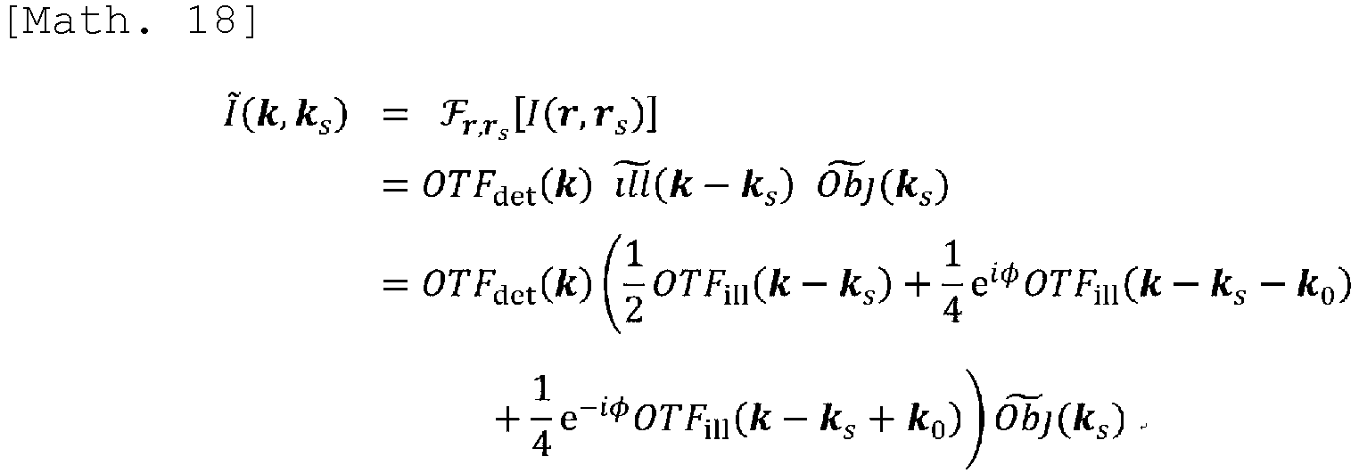
- In the expression (18), Fr,rs represents Fourier transformation of r and rs. OTFdet represents Fourier transformation of PSFdet and represents the OTF of the detection
optical system 5. ill∼ represents Fourier transformation of ill, OTFill represents Fourier transformation of PSFill, and Obj∼ represents Fourier transformation of Obj. The expression (18) is a sum of three terms as represented by the following expression (19).
Expression (19)
- In this case, I0∼(k,ks) of the first term on the right side of the expression (19) is referred to as the 0th-order component, I+1∼(k,ks) of the second term on the right side is referred to as the +lst-order component, and I-1∼(k,ks) of the third term on the right side is referred to as the - 1st-order component. These are the same as the data I0∼(k,ks) of the region AR1a of the Oth-order component, the data I+1∼(k,ks) of the region AR1b of the +lst-order component, and the data I-1∼(k,ks) of the region AR1c of the -1st-order component described above. Each of the 0th-order component, the +1st-order component, and the -1st-order component is represented by the following expression (20) .
Expression (20)
- The following describes a method of determining a region in which the Oth-order component, the +lst-order component, and the -1st-order component have values. In the expression (20), the cutoff frequency of OTFdet(k) is given as 2kNA em. The cutoff frequency of OTFill(k) is given as 2σkNA ex. Thus, OTFdet(k) has a value only in a range in which |k| is equal to or smaller than 2kNA em. Similarly, OTFill(k-ks) has a value only in a range in which |k-ks| is equal to or smaller than 2σkNA e. OTFill(k-ks-k0) has a value only in a range in which |k-ks-k0| is equal to or smaller than 2σkNA ex. OTFill(k-ks+k0) has a value only in a range in which |k-ks+k0| is equal to or smaller than 2σkNA ex. These regions are illustrated in
Fig. 10 . - Thus, to separate I0∼(k,ks), I+1∼(k,ks), and I-1∼(k,ks) from I∼(k,ks), each value of the regions represented by the respective expressions (13) to (15) may be extracted. Each of the region AR1a of the Oth-order component, the region AR1b of the +lst-order component, and the region AR1c of the -1st-order component may be larger or smaller than the region represented by each of the expressions (13) to (15). Also in a case in which the
opening 15a and theopening 15b of themask 15 have a shape other than a circular shape, the region in which component separation is performed can be determined by calculating a region in which OTFdet and OTFill have values by theoretical calculation, simulation, and the like. - I0∼(k,ks), I+1∼(k,ks), and I-1∼(k,ks) that are returned to the real space by inverse Fourier transformation are respectively assumed to be I0(r,rs), I+1(r,rs), and I-1(r,rs). By performing inverse Fourier transformation on k and ks in the expression (20) described above, the following expression (21) is obtained.
Expression (21)
- The
image processor 7 performs the processing represented by the expression (16) and the expression (17) described above on results of component separation and inverse Fourier transformation. In this way, the phase of the interference fringes L2 is shifted in accordance with the detector coordinates r. The shift amount of the phase of the interference fringes is determined so that a peak position of a function obtained as a product of PSFdet(r+rs) and PSFill(rs) and the peak of the interference fringes substantially match each other, for example. - The deviation amount of the phase of the interference fringes is determined as follows, for example. The
image processor 7 calculates a positional deviation amount of a signal detected at the detector coordinates r. Theimage processor 7 calculates the positional deviation amount described above by obtaining the peak position of the function obtained as a product of PSFdet(r+rs) and PSFill(rs). In this case, the positional deviation of the effective PSF can be considered to be proportional to the detector coordinates r. A parameter representing a degree of deviation is assumed to be β, and the positional deviation amount is represented as r/β. - A value of β may be calculated from the peak position of the function obtained as a product of PSFdet(r+rs) and PSFill(rs) or may be calculated by numerical simulation. When β is determined, the phase shift amount corresponding to the detector coordinates is determined. The phase shift amount ψ(r) of the interference fringes L2 is determined so that the peak position of the function obtained as a product of PSFdet(r+rs) and PSFill(rs) matches the peak position of the interference fringes. Through such processing, the phase shift amount is represented as ψ(r) = -2πk0.r/β-φ, for example. A value of an initial phase φ may be a value that is measured in advance by using fluorescent beads or may be a value estimated from an observation image. The
image processor 7 determines a conversion amount of the phase (phase shift amount) on the basis of the light intensity distribution of the excitation light on the sample S. Theimage processor 7 determines the phase shift amount on the basis of the electric field intensity ill(r) of the excitation light on the sample plane Sa as the light intensity distribution of the excitation light on the sample S. By using ψ(r) that is set as described above, distortion of the shape of the effective PSF for each position r of thedetector 6a is corrected after the processing represented by the expression (16) and the expression (17). - After performing the phase shift processing as described above, the
image processor 7 performs processing of correcting the positional deviation of the effective PSF for eachdetector 6a. When the processing of correcting the positional deviation is performed, the effective PSFs of the images of therespective detectors 6a of thedetection device 6 become substantially the same. Theimage processor 7 generates the super resolution image ISR(rs) by adding up the images of therespective detectors 6a of thedetection device 6. This series of processing is represented by the following expression (22).
Expression (22)
- In the expression (22), PH(r) represents a pinhole function defined by the following expression (23).
Expression (23)
- By adjusting a value of rPH, a signal amount and a sectioning effect can be adjusted. When rPH is increased, the signal amount is increased. When rPH is reduced, the sectioning capacity is improved. PSFSR(rs) as the effective PSF of the image obtained by the arithmetic operation of the expression (22) described above is represented by the following expression (24).
Expression (24)
- Focusing on the periodic direction of the interference fringes L2, that is, the k0-direction, it can be found that the full width at half maximum of the PSFeff becomes narrower and the resolving power is improved as the period of the interference fringes L2 is smaller on the basis of the expression (24). That is, as the number of fringes (bright parts) included in the periodic direction of the interference fringes L2 according to the embodiment is increased, the full width at half maximum of the PSFeff is reduced and the resolving power is improved. The full width at half maximum of a conventional fluorescence microscope is given as 0.51λem/NA. The full width at half maximum of the PSFeff according to the embodiment is 0.3λex/NA in a case in which σ = 0.3, for example, and the full width at half maximum of the PSF is 1.7 times narrower and the resolving power is improved as compared with the conventional fluorescence microscope. The number of bright parts included in the periodic direction of the interference fringes L2 according to the embodiment is 5 in a case in which σ = 0.3, for example. The full width at half maximum of the PSFeff according to the embodiment is 0.34λex/NA in a case in which σ = 0.4, for example, and the full width at half maximum of the PSF is 1.5 times narrower and the resolving power is improved as compared with the conventional fluorescence microscope. The number of bright parts included in the periodic direction of the interference fringes L2 according to the embodiment is 3 in a case in which σ = 0.4, for example. In a case of sufficiently reducing an aperture of a pinhole of a conventional confocal microscope, it is known that the full width at half maximum of the PSF becomes 1.4 times narrower and the resolving power is improved as compared with the conventional fluorescence microscope. To hold superiority in the effect of improving the resolving power, the full width at half maximum of the PSF of the confocal microscope is preferably 1.5 times or more narrower as compared with the conventional fluorescence microscope. That is, the number of bright parts included in the periodic direction of the interference fringes L2 according to the embodiment is preferably equal to or larger than 3. The same applies to the other embodiments.
- In the present embodiment, a scanning interval and the interval between the
detectors 6a of thedetection device 6 may be set on the basis of the cutoff frequency and Nyquist's theorem. The scanning interval may be set to be equal to or smaller than λex/8NA in the periodic direction of the interference fringes. The scanning interval may also be set to be equal to or smaller than λex/4NA in a direction perpendicular to the periodic direction of the interference fringes. The interval between thedetectors 6a of thedetection device 6 may be set to be equal to or smaller than λem/4NA. -
Fig. 11 is a flowchart illustrating the observation method according to the third embodiment. The processing from Step S1 to Step S4 is the same as that inFig. 6 , so that description thereof is omitted. In Step S21, theimage processor 7 performs Fourier transformation on at least some of the detection results of thedetectors 6a. In Step S21, theimage processor 7 performs four-dimensional Fourier transformation on I(r,rs). In Step S22, theimage processor 7 performs component separation in the frequency space. Theimage processor 7 separates the component of the frequency space obtained by Fourier transformation for each region of the frequency space. In Step S23, theimage processor 7 performs inverse Fourier transformation on the separated component. In Step S24, theimage processor 7 performs phase shift processing. In Step S25, theimage processor 7 corrects the positional deviation of the effective PSF. In Step S26, theimage processor 7 generates an image (for example, a super resolution image) by adding up the images that are obtained by correcting the positional deviation in Step S25. - In this way, the
image processor 7 according to the present embodiment generates the image by converting the phase of at least part of the data obtained through the component separation. In the above description, theimage processor 7 performs phase shift processing on the data in the real space. That is, theimage processor 7 uses, as the data obtained through the component separation, data (data in the real space) that is obtained by converting the data subjected to component separation (data in the frequency space) into the data in the real space by inverse Fourier transformation. Theimage processor 7 may perform, in the frequency space, phase shift processing on the data in the frequency space subjected to component separation. - The following describes a fourth embodiment. In the present embodiment, a configuration similar to that in the embodiments described above is denoted by the same reference numeral, and description thereof is omitted or simplified as appropriate. In the present embodiment, the image processor 7 (refer to
Fig. 4 ) performs component separation described in the third embodiment and performs deconvolution on the separated component thereafter to generate an image. - By substituting the expression (20) for the expression (19) described above, the following expression (25) is obtained.
Expression (25)
- In the expression (25), OTF0(k,ks), OTF+1(k,ks), and OTF-1(k,ks) are represented by the following expression (26) .
Expression (26)
- The
image processor 7 performs deconvolution using an estimated value of each of OTF0(k,ks), OTF+1(k,ks), and OTF-1(k,ks). There are known various methods of deconvolution such as a Wiener filter and a Richardson-Lucy method. The following describes processing using the Wiener filter as an example of deconvolution, but any other method can be used for deconvolution. Deconvolution for the expression (25) described above using the Wiener filter is represented by the following expression (27).
Expression (27)
- In the expression (27), A(ks) is an apodization function for suppressing a negative value of the image. w is a Wiener parameter for suppressing noise. Fks -1 is inverse Fourier transformation of ks. The
image processor 7 generates the image using a result of deconvolution described above. -
Fig. 12 is a flowchart illustrating the observation method according to the fourth embodiment. The processing from Step S1 to Step S4 is the same as that inFig. 6 , so that description thereof is omitted. In Step S31, theimage processor 7 performs Fourier transformation on the detection result. In Step S32, theimage processor 7 separates the component in the frequency space. In Step S33, theimage processor 7 performs deconvolution using the component separated through the processing in Step S32. In Step S34, theimage processor 7 performs apodization. In Step S35, theimage processor 7 performs inverse Fourier transformation on data obtained through deconvolution and apodization. Theimage processor 7 generates the image using data obtained through inverse Fourier transformation. - As described above, the
image processor 7 according to the present embodiment performs component separation, deconvolution, and apodization in the frequency space, and converts the data obtained through these pieces of processing into data in the real space to generate the image. In the present embodiment, theimage processor 7 may generate the image without performing processing of causing the effective PSFs of therespective detectors 6a of thedetection device 6 to substantially match each other to correct a positional deviation. - In the present embodiment, the scanning interval and the interval between the
detectors 6a of thedetection device 6 may be set on the basis of the cutoff frequency and Nyquist's theorem. The scanning interval may be set to be equal to or smaller than λex/8NA in the periodic direction of the interference fringes. The scanning interval may be set to be equal to or smaller than λex/4NA in a direction perpendicular to the periodic direction of the interference fringes. The interval between thedetectors 6a of thedetection device 6 may be set to be equal to or smaller than λem/4NA. - The
image processor 7 may set a range of k as an addition target to be a range of the entire space, or to be a partial range of the entire space. Theimage processor 7 may limit a range of r at the time of performing arithmetic operation on I0∼(k,ks), I+1∼(k,ks), and I-1∼(k,ks) by Fourier transformation. Theimage processor 7 may use, as OTF0(k,ks), OTF+1(k,ks), and OTF-1(k,ks), data that is obtained in advance by measurement using fluorescent beads, numerical simulation using a design value, or the like, or data (for example, an estimated value) that is obtained from a result obtained by detecting fluorescence from the sample S by thedetection device 6. - The following describes a fifth embodiment. In the present embodiment, a configuration similar to that in the embodiments described above is denoted by the same reference numeral, and description thereof is omitted or simplified as appropriate.
Fig. 13 is a diagram illustrating the microscope according to the fifth embodiment. In the present embodiment, thedetection device 6 includes a line sensor (line detector) in which thedetectors 6a are one-dimensionally arranged. Thedetectors 6a are arranged in one direction in thedetection device 6. Thedetection device 6 is disposed at a position that is optically conjugate to the sample plane Sa. The direction in which thedetectors 6a are arranged (hereinafter, referred to as an arrangement direction) is set to be a direction corresponding to the periodic direction of the interference fringes L2. For example, inFig. 13 , the periodic direction of the interference fringes is the X-direction, and the arrangement direction of thedetectors 6a is set to be the Xb-direction corresponding to the X-direction. - The
microscope 1 according to the present embodiment includes a λ/2wave plate 30 and anoptical path rotator 31 that causes the optical path to rotate about the optical axis. The λ/2wave plate 30 causes polarized light passing through theoptical path rotator 31 to rotate on the basis of a rotation angle of the optical path rotated by theoptical path rotator 31. Theoptical path rotator 31 is disposed on the optical path between themask 15 and the sample S in the illuminationoptical system 4. Theoptical path rotator 31 is, for example, disposed at a position at which the excitation light L1 becomes substantially parallel light on the optical path in the illuminationoptical system 4. Theoptical path rotator 31 is, for example, disposed at a position through which the excitation light L1 passes in the illuminationoptical system 4 and the fluorescence L3 passes in the detectionoptical system 5. Theoptical path rotator 31 is, for example, disposed on the optical path between thedichroic mirror 16 and the sample S. The λ/2wave plate 30 may be disposed on the same side as the sample S with respect to theoptical path rotator 31, or may be disposed on the opposite side of the sample S (for example, on the same side as the light source of the excitation light) with respect to theoptical path rotator 31. - The
optical path rotator 31 is, for example, an image rotator such as a Dove prism. Theoptical path rotator 31 is disposed to be able to rotate about the optical axis of the illuminationoptical system 4. Theoptical path rotator 31 is driven by adriver 32 to rotate. In a case of using the Dove prism as theoptical path rotator 31, when the Dove prism is rotated about the optical axis of the illuminationoptical system 4 by θ°, the optical path on a light emitting side of the Dove prism (on the sample S side) is rotated about the optical axis of the illuminationoptical system 4 by 2×θ° with respect to the optical path on a light incident side of the Dove prism (on thelight source 3 side). Due to this, the incident plane of the excitation light L1 for the sample S is rotated about the Z-direction by 2×θ°, and the periodic direction of the interference fringes L2 is rotated about the Z-direction by 2×θ°. For example, in a case of changing the periodic direction of the interference fringes L2 by 90°, thedriver 32 causes theoptical path rotator 31 to rotate about the optical axis of the illuminationoptical system 4 by 45°. In this way, theoptical path rotator 31 is included in the fringe direction changer that changes the direction of the interference fringes with respect to the sample. - The λ/2
wave plate 30 is disposed to be able to rotate about the optical axis of the illuminationoptical system 4. The λ/2wave plate 30 rotates interlocking with theoptical path rotator 31. The λ/2wave plate 30 rotates by an angle that is defined on the basis of a rotation angle of theoptical path rotator 31. For example, the λ/2wave plate 30 is fixed to (for example, integrated with) theoptical path rotator 31, and rotates together with theoptical path rotator 31. In this case, the λ/2wave plate 30 rotates by the same angle as the rotation angle of theoptical path rotator 31. - When the λ/2
wave plate 30 is rotated about the optical axis of the illuminationoptical system 4 by θ°, the polarization direction of the excitation light L1 is rotated about the optical axis of the illuminationoptical system 4 by 2×θ° with respect to the polarization direction on the light incident side (light source 3 side). Due to this, the polarization state of the excitation light L1 at the time of being incident on the sample S becomes S-polarization. - The
optical path rotator 31 inFig. 13 is also included in an image rotator. The image rotator causes an image of the sample S (for example, an image of fluorescence from the sample S) to rotate about the optical axis of the detectionoptical system 5 with respect to thedetectors 6a. That is, the fringe direction changer and the image rotator include theoptical path rotator 31 as the same member (optical member). Theoptical path rotator 31 is disposed at a position on which fluorescence is incident on the optical path of the illuminationoptical system 4. The image rotator causes the image of fluorescence to rotate with theoptical path rotator 31. Theoptical path rotator 31 adjusts the periodic direction of the interference fringes L2 with respect to the arrangement direction of thedetectors 6a of thedetection device 6. In a case of using the Dove prism as theoptical path rotator 31, when the Dove prism is rotated about the optical axis of the illuminationoptical system 4 by θ°, the periodic direction of the interference fringes L2 is rotated about the Z-direction by 2×θ°. The optical path of the fluorescence L3 from the sample S is then rotated by - 2×θ° on the light emitting side (detection device 6 side) with respect to the light incident side (sample S side) of the Dove prism. - When the Dove prism is rotated, the optical path of light traveling toward the sample S via the Dove prism is rotated, and the periodic direction of the interference fringes L2 with respect to the sample S is changed. The optical path of the light traveling from the sample S toward the
detection device 6 via the Dove prism is rotated in the opposite direction of the optical path of the light traveling toward the sample S by the same angle. Thus, in a case of projecting images of thedetectors 6a (for example, line detectors) of thedetection device 6 on the sample plane Sa via the detectionoptical system 5, the direction in which thedetectors 6a are arranged always matches the periodic direction of the interference fringes even in a case in which the periodic direction of the interference fringes is changed by the Dove prism. Thus, thedetection device 6 can detect the fluorescence L3 before and after the periodic direction of the interference fringes L2 is changed. Theimage processor 7 generates the image through the processing described in the first embodiment to the fourth embodiment on the basis of the detection result of thedetection device 6. - In the
microscope 1 according to the first embodiment, thedriver 22 causes themask 15 to rotate to change the periodic direction of the interference fringes L2, but the periodic direction of the interference fringes L2 may be changed by the optical path rotator 31 (for example, the Dove prism) described above. The fringe direction changer that changes the periodic direction of the interference fringes L2 may have a form different from both of thedriver 22 and theoptical path rotator 31. For example, thestage 2 may be disposed to be able to rotate about the Z-direction, and the direction of the interference fringes L2 with respect to the sample S may be changed by rotation of thestage 2. In this case, thestage 2 is included in the fringe direction changer that changes the direction of the interference fringes L2 with respect to the sample S. - The
microscope 1 illustrated inFig. 14 is different from that inFig. 13 in the position at which theoptical path rotator 31 is disposed. InFig. 14 , the fringe direction changer is the same as that in the first embodiment and includes themask 15 and thedriver 22. Theoptical path rotator 31 serves as both of the fringe direction changer and the image rotator inFig. 13 but is disposed separately from the fringe direction changer inFig. 14 . InFig. 14 , theoptical path rotator 31 is disposed at a position not overlapping with the optical path of the illuminationoptical system 4 on the optical path of the detectionoptical system 5. Theoptical path rotator 31 is disposed at a position on which the excitation light L1 is not incident but the fluorescence L3 is incident. Theoptical path rotator 31 is disposed on the optical path between thedichroic mirror 16 and thedetection device 6. - In the
microscope 1, the periodic direction of the interference fringes L2 is changed when thedriver 22 causes themask 15 and thepolarizer 14 to rotate. Thedriver 32 causes theoptical path rotator 31 to rotate by an angle that is defined on the basis of rotation angles of themask 15 and thepolarizer 14. In themicroscope 1, thedriver 32 causes theoptical path rotator 31 to rotate to cause a direction of an image projected on thedetection device 6 to match the direction in which thedetectors 6a are arranged. - The following describes a sixth embodiment. In the present embodiment, a configuration similar to that in the embodiments described above is denoted by the same reference numeral, and description thereof is omitted or simplified as appropriate.
Fig. 15 is a diagram illustrating the microscope according to the sixth embodiment. In the present embodiment, themicroscope 1 includes alight shielding member 33. Thelight shielding member 33 is disposed at a position that is optically conjugate to the sample plane Sa or in the vicinity thereof. InFig. 15 , thedetection device 6 is disposed at a position that is optically conjugate to the sample plane Sa, and thelight shielding member 33 is disposed in the vicinity of thedetection device 6. Thelight shielding member 33 may be disposed at a position that is conjugate to the sample plane Sa or in the vicinity thereof. - The
light shielding member 33 has anopening 33a through which the fluorescence L3 passes and blocks the fluorescence L3 around theopening 33a. Theopening 33a extends in the arrangement direction (Xb-direction) of thedetectors 6a in thedetection device 6. Theopening 33a is, for example, a slit having a rectangular shape. Thelight shielding member 33 is disposed so that a long side of theopening 33a becomes substantially parallel with the arrangement direction of thedetectors 6a. One or both of dimensions and a shape of theopening 33a of thelight shielding member 33 may be variable. For example, thelight shielding member 33 may be a mechanical diaphragm that can change a light shielding region, a spatial light modulator (SLM), or the like. One or both of the dimensions and the shape of theopening 33a may be fixed. - The
detection device 6 detects the fluorescence L3 passed through theopening 33a of thelight shielding member 33. Theimage processor 7 generates an image on the basis of a detection result of thedetection device 6. Theimage processor 7 may perform any of the pieces of processing described in the first embodiment to the fourth embodiment. Herein, the following describes a case in which the phase of the PSFs of the interference fringes L2 is shifted through image processing. - In the present embodiment, image data I(x,rs) corresponding to the detection result of the
detection device 6 is represented by the following expression (28).
Expression (28)
- I(x,rs) is three-dimensional data having detector coordinates x corresponding to the position of the
detector 6a in thedetection device 6 and the scan coordinates (xs,ys) as independent variables. In the expression (28), PHy(ys) represents a pinhole function representing influence of thelight shielding member 33. PHy(ys) is represented by the following expression (29).
Expression (29)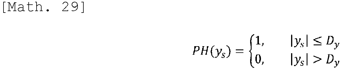
- In the expression (29), Dy is a half of the width of the
opening 33a of thelight shielding member 33 in the Yb-direction (refer toFig. 17 ). That is, the width of theopening 33a of thelight shielding member 33 in the Yb-direction (refer toFig. 17 ) is assumed to be 2Dy. - The processing performed by the
image processor 7 described in the present embodiment can also be applied to the case in which thelight shielding member 33 is not disposed as illustrated inFig. 13 . In the case in which thelight shielding member 33 is not disposed, PHy(ys) = 1 may be established for the entire range of ys in accordance with the fact that Dy is infinite. In the case in which thelight shielding member 33 is not disposed, the width in the Yb-direction of the optical path of the fluorescence L3 at the time of being incident on thedetector 6a corresponds to the dimension in the Yb-direction of thedetector 6a, and a half value of the dimension in the Yb-direction of thedetector 6a may be used as a value of Dy. - By performing Fourier transformation on x, xs, and ys in the expression (28) described above, the following expression (30) is obtained. In the expression (30), PHy∼(kys) represents Fourier transformation of PHy(ys). ky represents an integration variable of convolution.
Expression (30)
- In this case, for convenience of explanation, an illumination shape is assumed to be represented by the expression (2) described above, and the periodic direction of the interference fringes L2 is assumed to be the X-direction. ill∼(kx-kxs, ky-kys) in the expression (30) is represented by the following expression (31). In the expression (31), φ represents the initial phase of the interference fringes L2.
Expression (31)
- By substituting the expression (31) for the expression (30) to be organized, I∼(kx,kxs,kys) is represented by the following expression (32).
Expression (32)
- In the expression (32), I∼0(kx,kxs,kys) corresponds to the Oth-order component described in the third embodiment, I∼+1(kx,kxs,kys) corresponds to the +lst-order component, and I∼-1(kx,kxs,kys) corresponds to the -1st-order component. Regions in which I∼0(kx,kxs,kys), I∼+1(kx,kxs,kys), and I∼-1(kx,kxs,kys) have respective values are different from each other.
-
Fig. 16 is a diagram illustrating a region of the frequency space used for component separation according to the sixth embodiment. Ranges in the kys-direction of the regions in which the Oth-order component, the +lst-order component, and the -1st-order component have respective values depend on PHy∼ and OTFdet.Fig. 16 illustrates the regions in which the components have respective values in a case in which theopening 15a and theopening 15b of the mask 15 (refer toFig. 2 ) have a circular shape. In a case in which the opening of themask 15 has a shape other than the circular shape, it is possible to obtain Fourier transformation of ill, and calculate the range of the region in which each component has a value on the basis of the expression (30). As a method of calculating the range of the region in which each component has a value, analytic calculation, numerical simulation, or the like may be performed. - In
Fig. 16 , each of the region AR1a of the Oth-order component, the region AR1b of the +lst-order component, and the region AR1c of the -1st-order component is a region having an elliptic shape on the kxs-kys plane. The region AR1a of the Oth-order component, the region AR1b of the +lst-order component, and the region AR1c of the -1st-order component have the same width in the kxs-direction on the kxs-kys plane. The width of the region AR1a of the 0th-order component is 4σkNA ex. The region AR1a of the 0th-order component is a region centered on an origin. Each of the region AR1b of the +lst-order component and the region AR1c of the -1st-order component is a region having the center on the axis of kxs. A distance between the center of the region AR1c of the -1st-order component and the origin is 2(1 - σ)kNA ex. The region AR1c of the +lst-order component is a region at a position symmetrical to the region AR1c of the -1st-order component with respect to the region AR1a of the Oth-order component. - The
image processor 7 extracts each component from I∼(kx,kxs,kys). For example, theimage processor 7 extracts data of the region AR1a of the Oth-order component from I∼(kx,kxs,kys) to separate I0∼(kx,kxs,kys) therefrom. Theimage processor 7 extracts data of the region AR1b of the +lst-order component from I∼(kx,kxs,kys) to separate I+1∼(kx,kxs,kys) therefrom. Theimage processor 7 extracts data of the region AR1c of the -1st-order component from I∼(kx,kxs,kys) to separate I-1∼(kx,kxs,kys) therefrom. - The
image processor 7 performs inverse Fourier transformation on each of I0∼(kx,kxs,kys), I+1∼(kx,kxs,kys), and I-1∼(kx,kxs,kys) that are obtained through component separation, and calculates data of each component in the real space. The data obtained by performing inverse Fourier transformation on I0∼(kx,kxs,kys) is represented as I0(x,xs,ys), data obtained by performing inverse Fourier transformation on I+1∼(kx,kxs,kys) is represented as I+1(x,xs,ys), and data obtained by performing inverse Fourier transformation on I-1∼(kx,kxs,kys) is represented as I-1(x,xs,ys). - The
image processor 7 shifts the phase of the interference fringes in accordance with the detector coordinates so that the effective PSFs of therespective detectors 6a of thedetection device 6 are aligned by using at least part of the data of the respective components in the real space obtained as described above. Theimage processor 7 shifts the phase of the interference fringes L2 by arithmetic operations represented by the following expressions (33) and (34).
Expression (33)
Expression (34)
- After the phase shift processing, similarly to the third embodiment, the
image processor 7 performs correction processing of collecting the positional deviation. After the correction processing, theimage processor 7 generates a super resolution image by adding up images of the respective detectors. - The following describes a seventh embodiment. In the present embodiment, a configuration similar to that in the embodiments described above is denoted by the same reference numeral, and description thereof is omitted or simplified as appropriate.
Fig. 17 is a diagram illustrating the microscope according to the seventh embodiment. In the present embodiment, themicroscope 1 includes thedriver 22 and adriver 34. Thedriver 22 is the same as that in the first embodiment. Thedriver 22 causes themask 15 to rotate to change the periodic direction of the interference fringes L2. Thedriver 22 is included in the fringe direction changer that changes the direction of the interference fringes L2 with respect to the sample S. - In the present embodiment, the
detection device 6 can rotate about the Zb-direction. Thedriver 34 causes thedetection device 6 to rotate about the Zb-direction. Thedriver 34 causes thedetection device 6 to rotate so that the arrangement direction of thedetectors 6a in thedetection device 6 corresponds to the periodic direction of the interference fringes L2. For example, in a case in which thedriver 22 causes themask 15 to rotate by 90°, the periodic direction of the interference fringes L2 is changed by 90°, so that thedriver 34 causes thedetection device 6 to rotate by 90°. - The
driver 34 causes thelight shielding member 33 to rotate so that relative positions of thedetection device 6 and thelight shielding member 33 are maintained. For example, thelight shielding member 33 is integrated with thedetection device 6, and thedriver 34 causes thelight shielding member 33 and thedetection device 6 to integrally rotate. - The
microscope 1 may include theoptical path rotator 31 illustrated inFig. 14 instead of causing thedetection device 6 to rotate. Themicroscope 1 does not necessarily include thelight shielding member 33 as illustrated inFig. 13 . - The following describes an eighth embodiment. In the present embodiment, a configuration similar to that in the embodiments described above is denoted by the same reference numeral, and description thereof is omitted or simplified as appropriate.
Fig. 18 is a diagram illustrating the microscope according to the eighth embodiment. In the embodiment described above, exemplified is a case in which the illumination pupil is divided into two poles (two regions) on the pupil plane P0 (refer toFig. 2(C) ), but the illumination pupil may have another form. The following describes a form in which the illumination pupil is divided into four poles (four regions) on the pupil plane. - The illumination
optical system 4 according to the present embodiment includes thecollimator lens 12, a λ/2wave plate 35, a polarizedlight separating element 36, amirror 37, a mask 38 (opening member), amirror 39, a mask 40 (opening member), and a polarizedlight separating element 41 on the light emitting side of theoptical fiber 11. The configuration from thedichroic mirror 16 to theobjective lens 21 of the illuminationoptical system 4 is the same as that in the first embodiment. - The excitation light L1 emitted from the
optical fiber 11 is converted into substantially parallel light by thecollimator lens 12 and is incident on the λ/2wave plate 35. The excitation light L1 passed through the λ/2wave plate 35 includes excitation light L1c as linearly polarized light in a first direction and excitation light L1d as linearly polarized light in a second direction. A direction of an optical axis (a fast axis, a slow axis) of the λ/2wave plate 35 is set so that a ratio between an amount of the excitation light L1c and an amount of the excitation light L1d becomes a predetermined ratio. - The excitation light L1 (the excitation light L1c and the excitation light L1d) passed through the λ/2
wave plate 35 is incident on the polarizedlight separating element 36. The polarizedlight separating element 36 includes a polarizedlight separation film 36a that is inclined with respect to theoptical axis 12a of thecollimator lens 12. The polarizedlight separation film 36a has a characteristic of reflecting the linearly polarized light in the first direction and transmitting the linearly polarized light in the second direction. The polarizedlight separating element 36 is, for example, a polarized beam splitter prism (PBS prism). The linearly polarized light in the first direction described above is S-polarized light with respect to the polarizedlight separation film 36a. The linearly polarized light in the second direction described above is P-polarized light with respect to the polarizedlight separation film 36a. - The excitation light L1c as S-polarized light with respect to the polarized
light separation film 36a is reflected by the polarizedlight separation film 36a and is incident on themask 38 via themirror 37. The excitation light L1d as P-polarized light with respect to the polarizedlight separation film 36a is transmitted through the polarizedlight separation film 36a and is incident on themask 40 via themirror 39. Each of themask 38 and themask 40 is a light flux splitter that splits the excitation light that excites a fluorescent substance into a plurality of light fluxes. Themask 38 and themask 40 will be described later with reference toFig. 19 . - Each of the excitation light L1c passed through the
mask 38 and the excitation light L1d passed through themask 40 is incident on the polarizedlight separating element 41. The polarizedlight separating element 41 includes a polarizedlight separation film 41a that is inclined with respect to the optical path of the excitation light L1c and the optical path of the excitation light L1d. The polarizedlight separation film 41a has a characteristic of reflecting the linearly polarized light in the first direction and transmitting the linearly polarized light in the second direction. The polarizedlight separating element 41 is, for example, a polarized beam splitter prism (PBS prism). The linearly polarized light in the first direction described above is S-polarized light with respect to the polarizedlight separation film 41a. The linearly polarized light in the second direction described above is P-polarized light with respect to the polarizedlight separation film 41a. - The excitation light L1c is S-polarized light with respect to the polarized
light separation film 41a and is reflected by the polarizedlight separation film 41a to be incident on thedichroic mirror 16. The excitation light L1d is P-polarized light with respect to the polarizedlight separation film 41a and is transmitted through the polarizedlight separation film 41a to be incident on thedichroic mirror 16. One or both of the polarizedlight separating element 36 and the polarizedlight separating element 41 are not necessarily the PBS prism. One or both of the polarizedlight separating element 36 and the polarizedlight separating element 41 may be a photonic crystal and the like having different characteristics of reflection and transmission for TE-polarized light and TM-polarized light. -
Fig. 19 is a diagram illustrating the mask and the polarization state of the excitation light according to the eighth embodiment. InFig. 19(A) , the Xc-direction, the Yc-direction, and the Zc-direction are directions respectively corresponding to the X-direction, the Y-direction, and the Z-direction on the sample plane Sa (refer toFig. 18 ). Themask 38 has anopening 38a and anopening 38b. Themask 38 is disposed on a pupil plane conjugate plane, or within a range distant therefrom by 100 mm or less. Theopening 38a and theopening 38b are arranged in the Xc-direction. Each of theopening 38a and theopening 38b has a circular shape, for example, but may have a shape other than the circular shape. - In
Fig. 19(B) , the Xd-direction, the Yd-direction, and the Zd-direction are directions respectively corresponding to the X-direction, the Y-direction, and the Z-direction on the sample plane Sa (refer toFig. 18 ). Themask 40 is disposed on the pupil plane conjugate plane, or within a range distant therefrom by 100 mm or less. Themask 38 or themask 40 may be disposed on the pupil plane, or within a range distant therefrom by 100 mm or less. Themask 40 has anopening 40a and anopening 40b. Theopening 40a and theopening 40b are arranged in the Yd-direction. Each of theopening 40a and theopening 40b has a circular shape, for example, but may have a shape other than the circular shape. - In
Fig. 19(C) , the reference numeral AR2a denotes a region on which the excitation light L1c passed through theopening 38a of themask 38 is incident on the pupil plane P0 of theobjective lens 21. The reference numeral AR2b denotes a region on which the excitation light L1c passed through theopening 38b of themask 38 is incident on the pupil plane P0. Each of arrows in the region AR2a and the region AR2b indicates a polarization direction of the excitation light L1c that is incident thereon. The region AR2a and the region AR2b are arranged in the X-direction. - Each of the excitation light L1c incident on the region AR2a and the excitation light L1c incident on the region AR2b is linearly polarized light in the Y-direction. The excitation light L1c incident on the region AR2a and the excitation light L1c incident on the region AR2b have the same polarization direction and interfere with each other on the sample plane Sa (refer to
Fig. 18 ). Due to this interference, the interference fringes the periodic direction of which is the X-direction is formed on the sample plane Sa. The incident plane of the excitation light L1c with respect to the sample plane Sa is the XZ-plane, and the excitation light L1c is incident on the sample S as S-polarized light. - In
Fig. 19(C) , the reference numeral AR2c denotes a region on which the excitation light L1d passed through theopening 40a of themask 40 is incident on the pupil plane P0. The reference numeral AR2d denotes a region on which the excitation light L1d passed through theopening 40b of themask 40 is incident on the pupil plane P0. Each of arrows in the region AR2c and the region AR2d indicates the polarization direction of the excitation light L1d that is incident thereon. The region AR2c and the region AR2d are arranged in the Y-direction. - Each of the excitation light L1d incident on the region AR2c and the excitation light L1d incident on the region AR2d is linearly polarized light in the X-direction. The excitation light L1d incident on the region AR2c and the excitation light L1d incident on the region AR2d have the same polarization direction and interfere with each other on the sample plane Sa (refer to
Fig. 18 ). Due to this interference, the interference fringes the periodic direction of which is the Y-direction is formed on the sample plane Sa. The incident plane of the excitation light L1d with respect to the sample plane Sa is the YZ-plane, and the excitation light L1c is incident on the sample S as S-polarized light. - Returning to the description of
Fig. 18 , the interference fringes L2 are formed on the sample plane Sa by combining the interference fringes generated by interference of the excitation light L1c and the interference fringes generated by interference of the excitation light L1d. Polarization directions of the excitation light L1c and the excitation light L1d are substantially orthogonal to each other, so that interference between the excitation light L1c and the excitation light L1d is suppressed. - The
detection device 6 detects the fluorescence L3 from the sample S via the detectionoptical system 5. As described in the first embodiment, thedetection device 6 is an image sensor in which thedetectors 6a are arranged in two directions, that is, the Xb-direction and the Yb-direction. Theimage processor 7 generates an image on the basis of a detection result of thedetection device 6. Herein, the following describes a case of shifting the phase of the PSFs of the interference fringes L2 through image processing. -
Fig. 20 is a diagram illustrating the pupil conjugate plane and the region of the frequency space used for component separation according to the eighth embodiment. InFig. 20(A) , the pupil conjugate plane P1 is represented in a wave coordinate space. kNA ex (a circle drawn by a dotted line) illustrated inFig. 20(A) represents a pupil radius of theobjective lens 21. Each of the region AR2a and the region AR2b on which the excitation light L1c is incident and the region AR2c and the region AR2d on which the excitation light L1d is incident is assumed to have a circular shape herein, but the shape thereof is not limited to the circular shape. A radius of each of the regions from the region ARa to the region ARd is σkNA ex. A distance between the center of each of the regions from the region ARa to the region ARd and theoptical axis 21a of theobjective lens 21 is (1 - σ)kNA ex. A distance between the center of the region AR2a and the center of the region AR2b is 2(1 - σ)kNA ex, for example, but the distance is not limited to this value. A distance between the center of the region AR2c and the center of the region AR2d is 2(1 - σ)kNA ex, for example, but the distance is not limited to this value. - The electric field intensity ill(r) on the sample plane Sa is represented by the following expression (35). In the expression (35), each of k0x and k0y is a wave vector of the interference fringes L2. k0x is represented as k0x = (k0,0). k0y is represented as k0y = (0, k0). k0 as a component of k0x and k0y is represented as k0 = 2(1 - σ) kNA ex.
Expression (35)
- In the present embodiment, the illumination pupil has four poles, and the interference fringes the periodic direction of which is the X-direction and the interference fringes the periodic direction of which is the Y-direction are added up. The image data I(r,rs) obtained by the
detection device 6 is represented by the following expression (36).
Expression (36)
- The
image processor 7 performs four-dimensional Fourier transformation on r and rs of I(r,rs) in the expression (36) as represented by the following expression (37) .
Expression (37)
- In the expression (37), OTFdet is Fourier transformation of PSFdet, and represents the OTF of the detection
optical system 5. ill∼ represents Fourier transformation of ill. OTFill represents Fourier transformation of PSFill. φx and φy represent the initial phase in the X-direction of the interference fringes L2 and the initial phase in the Y-direction of the interference fringes L2, respectively. Obj∼ represents Fourier transformation of Obj. The expression (37) is a sum of five terms as represented by the following expression (38).
Expression (38)
- Respective terms on the right side of the expression (38) are represented by the following expression (39).
Expression (39)
- In this case, I0∼(k,ks) is referred to as the 0th-order component, I∼+1,x(k,ks) is referred to as the +1st-order component in the X-direction, and I∼-1,x(k,ks) is referred to as the -1st-order component in the X-direction. I∼+1,y(k,ks) is referred to as the +lst-order component in the Y-direction, and I∼-1,y(k,ks) is referred to as the - 1st-order component in the Y-direction. In
Fig. 20(B) , the reference numeral AR3a denotes a region in which data of the Oth-order component is present (hereinafter, referred to as a region of the Oth-order component). The reference numeral AR3b denotes a region in which data of the +1st-order component in the X-direction is present (hereinafter, referred to as a region of the +lst-order component in the X-direction). The reference numeral AR3c denotes a region in which data of the -1st-order component in the X-direction is present (hereinafter, referred to as a region of the -1st-order component in the X-direction). The reference numeral AR3d denotes a region in which data of the +lst-order component in the Y-direction is present (hereinafter, referred to as a region of the +lst-order component in the Y-direction). The reference numeral AR3e denotes a region in which data of the -1st-order component in the Y-direction is present (hereinafter, referred to as a region of the -1st-order component in the Y-direction). - The region AR3a of the Oth-order component is represented by the following expression (40).
Expression (40)
- The region AR3b of the +lst-order component in the X-direction is represented by the following expression (41).
Expression (41)
- The region AR3c of the -1st-order component in the X-direction is represented by the following expression (42).
Expression (42)
- The region AR3d of the +lst-order component in the Y-direction is represented by the following expression (43).
Expression (43)
- The region AR3e of the -1st-order component in the Y-direction is represented by the following expression (44).
Expression (44)
- The
image processor 7 extracts, by filtering, each component from I∼(k,ks) that is obtained through Fourier transformation. For example, theimage processor 7 extracts data in a region satisfying the expression (40) described above from I∼(k,ks) as the Oth-order component. Theimage processor 7 extracts data in a region satisfying the expression (41) described above from I∼(k,ks) as the +lst-order component in the X-direction. Theimage processor 7 extracts data in a region satisfying the expression (42) described above from I∼(k,ks) as the -1st-order component in the X-direction. Theimage processor 7 extracts data in a region satisfying the expression (43) described above from I∼(k,ks) as the +lst-order component in the Y-direction. Theimage processor 7 extracts data in a region satisfying the expression (44) described above from I∼(k,ks) as the -1st-order component in the Y-direction. - The
image processor 7 calculates the data of each component in the real space by performing inverse Fourier transformation on each extracted component. In this case, the Oth-order component in the real space is represented as I0(r,rs), the +lst-order component in the X-direction in the real space is represented as I+1,x(r,rs), and the -1st-order component in the X-direction in the real space is represented as I-1,x(r,rs). The +lst-order component in the Y-direction in the real space is represented as I+1,y(r,rs), and the -1st-order component in the Y-direction in the real space is represented as I-1,y(r,rs). - By using at least part of the data of each component in the real space that is obtained as described above, the
image processor 7 shifts the phase of the interference fringes in accordance with the detector coordinates so that the effective PSFs of therespective detectors 6a of thedetection device 6 are aligned. Through an arithmetic operation represented by the following expression (45), theimage processor 7 shifts the phase of each of the +1st-order component in the X-direction, the -1st-order component in the X-direction, the +lst-order component in the Y-direction, and the -1st-order component in the Y-direction in the real space.
Expression (45)
- In the expression (45), ψx(r) represents the phase shift amount for each of the +lst-order component and the - 1st-order component in the X-direction. ψy(r) represents the phase shift amount for each of the +lst-order component and the -1st-order component in the Y-direction. The phase shift amount described above is, for example, set so that a peak position of a function obtained as a product of PSFdet(r+rs) and PSFill(rs) matches the peak position of the interference fringes L2.
- After the phase shift processing for each component, the
image processor 7 adds up the respective components as represented by the following expression (46).
Expression (46)
- Through the phase shift processing described above, it is possible to obtain data in which the effective PSFs of the
respective detectors 6a of thedetection device 6 are substantially aligned. After the phase shift processing, theimage processor 7 performs correction processing of correcting the positional deviation for each of thedetectors 6a. Theimage processor 7 then generates a super resolution image by adding up pieces of data subjected to the correction processing. - The region used for component separation is not limited to the regions represented by the expression (41) to the expression (44) described above. The region used for component separation may be larger or smaller than the regions represented by the expression (41) to the expression (44) described above. At least one of the
opening 38a and theopening 38b of themask 38 and theopening 40a and theopening 40b of themask 40 does not necessarily have a circular shape. The region used for component separation can be obtained by numerical simulation, theoretical calculation, and the like in both of a case in which the opening of the mask has a circular shape and a case in which the opening of the mask has a shape other than the circular shape. - The processing performed by the
image processor 7 may be any of the pieces of processing described in the first embodiment to the fourth embodiment. For example, in a case of applying deconvolution in the frequency space as described in the fourth embodiment, although the three components are used in the expression (27), five components including the Oth-order component, the +lst-order component in the X-direction, the -1st-order component in the X-direction, the +lst-order component in the Y-direction, and the -1st-order component in the Y-direction may be used in the present embodiment. - The following describes a ninth embodiment. In the present embodiment, a configuration similar to that in the embodiments described above is denoted by the same reference numeral, and description thereof is omitted or simplified as appropriate.
Fig. 21 is a diagram illustrating the microscope according to the ninth embodiment. In the present embodiment, themicroscope 1 includes the λ/2wave plate 30 and theoptical path rotator 31 described above with reference toFig. 13 . Theoptical path rotator 31 is driven by thedriver 32 to rotate about the optical axis of the illuminationoptical system 4. When theoptical path rotator 31 is rotated, each of the optical path of the excitation light L1c and the optical path of the excitation light L1d rotates about the optical axis of the illuminationoptical system 4. As a result, the periodic direction of the interference fringes L2 formed on the sample plane Sa is rotated about the Z-direction. -
Fig. 22 is a diagram illustrating the polarization state of the excitation light according to the ninth embodiment. InFig. 22(A) , regions AR4a on which the excitation light L1c is incident on the pupil plane P0 are arranged in the X-direction. A region AR4b and a region AR4b on which the excitation light L1d is incident on the pupil plane P0 are arranged in the Y-direction. -
Fig. 22(B) corresponds to a state in which the Dove prism (theoptical path rotator 31 inFig. 21 ) and the λ/2wave plate 30 are rotated by 22.5° from the state inFig. 22(A) . InFig. 22(B) , the regions AR4a on which the excitation light L1c is incident on the pupil plane P0 are arranged in a direction rotated from the X-direction by 45°. In this state, the periodic direction of the interference fringes of the excitation light L1c on the sample plane Sa is a direction rotated from the X-direction by 45°. The regions AR4b on which the excitation light L1d is incident on the pupil plane P0 are arranged in a direction rotated from the Y-direction by 45°. In this state, the periodic direction of the interference fringes of the excitation light L1d on the sample plane Sa is a direction rotated from the Y-direction by 45°. - Returning to the description of
Fig. 21 , in the present embodiment, thedetection device 6 detects the fluorescence L3 from the sample S before and after the periodic direction of the interference fringes L2 is changed. Theimage processor 7 generates an image on the basis of a detection result of thedetection device 6 before the periodic direction of the interference fringes L2 is changed and a detection result of thedetection device 6 after the periodic direction of the interference fringes L2 is changed. As described above with reference toFig. 14 , theoptical path rotator 31 may be disposed on the optical path between thedichroic mirror 16 and thedetection device 6. - The following describes a tenth embodiment. In the present embodiment, a configuration similar to that in the embodiments described above is denoted by the same reference numeral, and description thereof is omitted or simplified as appropriate. In the ninth embodiment, the
microscope 1 changes the periodic direction of the interference fringes L2 with theoptical path rotator 31, but the fringe direction changer that changes the periodic direction of the interference fringes L2 may have an aspect different from that of theoptical path rotator 31. -
Fig. 23 is a diagram illustrating the microscope according to the tenth embodiment.Fig. 24 is a diagram illustrating the mask according to the tenth embodiment. In the present embodiment, themicroscope 1 includes adriver 45 and adriver 46. Themask 38 can rotate about the optical axis of the excitation light L1c. Themask 38 is driven by thedriver 45 to rotate (refer toFig. 24(A) ). InFig. 24(A) , themask 38 is rotated clockwise by 45°. - The
mask 40 can rotate about the optical axis of the excitation light L1d. Themask 40 is driven by thedriver 46 to rotate (refer toFig. 24(B) ). Thedriver 46 causes themask 40 to rotate by the same angle as the angle of rotation of themask 38 rotated by thedriver 45. InFig. 24(B) , themask 40 is rotated clockwise by 45°. Due to this, the periodic direction of the interference fringes L2 on the sample plane Sa is rotated about the Z-direction by 45°. - A λ/2
wave plate 48 is disposed on the optical path between the polarizedlight separating element 41 and thedichroic mirror 16. The λ/2wave plate 48 is driven by adriver 49 to rotate about the optical axis of the illuminationoptical system 4. The λ/2wave plate 48 and thedriver 49 adjust each of the excitation light L1c and the excitation light L1d to be incident on the sample S as S-polarized light. - The following describes an eleventh embodiment. In the present embodiment, a configuration similar to that in the embodiments described above is denoted by the same reference numeral, and description thereof is omitted or simplified as appropriate.
Fig. 25 is a diagram illustrating the microscope according to the eleventh embodiment. In the present embodiment, themicroscope 1 includes a relayoptical system 47. The relayoptical system 47 is part of the illuminationoptical system 4 and is part of the detectionoptical system 5. The relayoptical system 47 is disposed on the optical path between the deflectingmirror 18a and the deflectingmirror 18b in thescanning part 18. The deflectingmirror 18a is disposed at substantially the same position as that of a first pupil conjugate plane that is optically conjugate to the pupil plane P0 of theobjective lens 21. The relayoptical system 47 is disposed so that a second pupil conjugate plane that is optically conjugate to the first pupil conjugate plane described above is formed between the deflectingmirror 18b and thelens 19. The deflectingmirror 18b is disposed at substantially the same position as that of the second pupil conjugate plane described above. - The
scanning part 18 is not limited to the form described above. For example, thestage 2 may include a Y-stage that moves in the Y-direction with respect to theobjective lens 21, and thescanning part 18 may include the Y-stage in place of the deflectingmirror 18b. In this case, thescanning part 18 may scan the sample S in the X-direction with the excitation light L1 by the deflectingmirror 18a and scan the sample S in the Y-direction with the excitation light L1 by moving the Y-stage. In this case, the deflectingmirror 18a may be disposed at substantially the same position as that of the pupil conjugate plane that is optically conjugate to the pupil plane P0 of theobjective lens 21. - The
stage 2 may include an X-stage that moves in the X-direction with respect to theobjective lens 21, and thescanning part 18 may include the X-stage in place of the deflectingmirror 18a. In this case, thescanning part 18 may scan the sample S in the X-direction with the excitation light L1 by moving the X-stage described above, and scan the sample S in the Y-direction with the excitation light L1 by the deflectingmirror 18b. In this case, the deflectingmirror 18b may be disposed at substantially the same position as that of the pupil conjugate plane that is optically conjugate to the pupil plane P0 of theobjective lens 21. - The
stage 2 may include the X-stage that moves in the X-direction with respect to theobjective lens 21 and the Y-stage that moves in the Y-direction with respect to theobjective lens 21, and thescanning part 18 may include the X-stage and the Y-stage described above. In this case, thescanning part 18 may scan the sample S in the X-direction with the excitation light L1 by moving the X-stage described above, and scan the sample S in the Y-direction with the excitation light L1 by moving the Y-stage described above. - In the embodiment described above, the scanning direction in which the sample S is scanned with the interference fringes includes two directions, that is, the X-direction and the Y-direction, and the illumination
optical system 4 two-dimensionally scans the sample S with the interference fringes. The scanning direction in which the sample S is scanned with the interference fringes may include three directions, that is, the X-direction, the Y-direction, and the Z-direction. For example, themicroscope 1 may perform 2D processing of scanning the sample S in the X-direction and the Y-direction with the interference fringes to acquire a 2D image, and repeat the 2D processing while changing the position in the Z-direction at which the interference fringes are generated to three-dimensionally scan the sample S with the interference fringes. By three-dimensionally scanning the sample S with the interference fringes, themicroscope 1 may acquire a plurality of 2D images the positions of which in the Z-direction are different, and generate a 3D image (for example, a Z-stack). In a case of three-dimensionally scanning the sample S with the interference fringes, the illuminationoptical system 4 may perform scanning in the X-direction and the Y-direction, and scanning in the Z-direction may be performed by moving thestage 2. The illuminationoptical system 4 may three-dimensionally scan the sample S with the interference fringes. - The following describes modifications. A configuration similar to that in the embodiments described above is denoted by the same reference numeral, and description thereof is omitted or simplified as appropriate.
Fig. 26 andFig. 27 are diagrams illustrating the illumination pupil according to modifications. - The illumination pupil has two poles in
Fig. 2 , four poles inFig. 20 , and three poles inFig. 26(A) . Each of the reference numeral AR5a to the reference numeral AR5c denotes a region on which the excitation light is incident on the pupil plane P0. In this case, formed are first interference fringes of the excitation light incident on the region AR5a and the excitation light incident on the region AR5b, second interference fringes of the excitation light incident on the region AR5b and the excitation light incident on the region AR5c, and third interference fringes of the excitation light incident on the region AR5c and the excitation light incident on the region AR5a. On the sample plane Sa, the interference fringes are formed by combining the first interference fringes, the second interference fringes, and the third interference fringes described above. In these sets of interference fringes, each of the periodic direction of the first interference fringes, the periodic direction of the second interference fringes, and the periodic direction of the third interference fringes is the periodic direction, and there are three periodic directions, so that the super resolution effect can be obtained in the three directions. The illumination pupil may have five or more poles. - The illumination pupil has a circular shape in
Fig. 2 , for example, but may have any other shape. InFig. 26(B) and Fig. 26(C) , the reference numeral AR6 denotes a region on which the excitation light is incident. The region AR6 inFig. 26(B) is a region surrounded by a circle AR6a as part of a circle centered on theoptical axis 21a of theobjective lens 21 and a straight line AR6b connecting both ends of the circular arc AR6a. The region AR6 inFig. 26(C) is a region surrounded by a circular arc as part of the circle centered on theoptical axis 21a of theobjective lens 21 and a curved line AR6c symmetrical to the circular arc AR6a. - In a case of the illumination pupil having the shape illustrated in
Fig. 26(B) or Fig. 26(C) , resolving power in a direction in which the interference fringes are not formed is improved, and sectioning is also improved as compared with a case of the illumination pupil having a circular shape. In a case of the illumination pupil having the shape illustrated inFig. 26(B) , resolving power in a direction in which the interference fringes are not formed is improved, and sectioning is also improved as compared with a case of the illumination pupil having the shape illustrated inFig. 26(C) . In a case of the illumination pupil having the shape illustrated inFig. 26(C) , resolving power in a direction in which the interference fringes are formed is improved as compared with a case of the illumination pupil having the shape illustrated inFig. 26(B) . - In
Fig. 27(A) , the illumination pupil has a form obtained by causing the illumination pupil having the shape illustrated inFig. 26(B) to have four poles. InFig. 27(B) , the illumination pupil has a form obtained by causing the illumination pupil having the shape illustrated inFig. 26(C) to have four poles. Also in a case of the illumination pupil having a shape other than the circular shape, the number of a plurality of regions (the number of poles) on which the excitation light is incident is set to be an optional number equal to or larger than 2. A shape of one of the regions on which the excitation light is incident on the pupil plane P0 may have a shape different from the shape of the other regions. Dimensions of one of the regions on which the excitation light is incident on the pupil plane P0 may be different from dimensions of the other regions. The regions on which the excitation light is incident on the pupil plane P0 may be disposed asymmetrical to each other with respect to theoptical axis 21a of theobjective lens 21. - The shape, the dimensions, and the arrangement of each pole of the illumination pupil can be implemented by designing the shape, the dimensions, and the arrangement of the opening of the
mask 15 illustrated inFig. 2 , for example. Themask 15 may be a mechanical diaphragm that can change a light shielding region, a spatial light modulator (SLM), or the like. -
Fig. 28 is a diagram illustrating the microscope according to a modification. InFig. 28 , the illuminationoptical system 4 includes acollimator lens 50, a λ/2wave plate 51, alens 52, adiffraction grating 53, alens 54, and themask 15 in this order from theoptical fiber 11 toward thedichroic mirror 16. Thecollimator lens 50 converts the excitation light L1 from theoptical fiber 11 into substantially parallel light. The λ/2wave plate 51 adjusts the polarization state of the excitation light L1 at the time of being incident on the sample S. Thelens 52 concentrates the excitation light L1 to thediffraction grating 53. - The
diffraction grating 53 causes the excitation light L1 to branch into a plurality of light fluxes by diffraction. Thediffraction grating 53 is a light flux splitter that splits the excitation light that excites a fluorescent substance into a plurality of light fluxes. Thediffraction grating 53 is disposed at a focal point of thelens 52, or within a range distant from the focal point by 1 mm or less. That is, thediffraction grating 53 is disposed on a plane that is conjugate to the sample plane Sa, or within a range distant therefrom by 1 mm or less. The light fluxes described above include Oth-order diffracted light, +lst-order diffracted light, and -1st-order diffracted light. Thelens 54 converts each of the Oth-order diffracted light, the +lst-order diffracted light, and the -1st-order diffracted light into substantially parallel light. Themask 15 is disposed so that the 0th-order diffracted light is blocked, and at least part of the +1-order diffracted light and at least part of the -1st-order diffracted light pass therethrough. In such a form, the amount of the excitation light L1 transmitted through themask 15 can be increased. Thediffraction grating 53 may be designed so that the Oth-order diffracted light is not generated. A configuration not including themask 15 may also be employed. -
Fig. 29 andFig. 30 are diagrams illustrating the polarization adjuster according to modifications. The optical path of the illuminationoptical system 4 is bent due to a reflection member such as thedichroic mirror 16 illustrated inFig. 1 , but the illuminationoptical system 4 is illustrated inFig. 29 andFig. 30 while being exploded to cause theoptical axis 4a to be a straight line. InFig. 29 andFig. 30 , the Z-direction is a direction parallel with theoptical axis 4a, and each of the X-direction and the Y-direction is a direction perpendicular to theoptical axis 4a. - In
Fig. 29 , the illuminationoptical system 4 includes a λ/4 wave plate 61, themask 15, and a λ/4 wave plate 62. The excitation light L1 emitted from theoptical fiber 11 is linearly polarized light substantially in the X-direction and is incident on the λ/4 wave plate 61. A polarizer (for example, a polarizing plate) having a transmission axis in the X-direction may be disposed on the optical path between theoptical fiber 11 and the λ/4 wave plate 61. - The fast axis of the λ/4 wave plate 61 is set in a direction obtained by rotating the X-direction counterclockwise by 45° when viewed from the +Z side. The excitation light L1 passed through the λ/4 wave plate 61 becomes circularly polarized light and is incident on the
mask 15. The excitation light L1 passed through theopening 15a and theopening 15b of themask 15 is circularly polarized light and is incident on the λ/4 wave plate 62. The fast axis of the λ/4 wave plate 62 is set in a direction obtained by rotating the X-direction clockwise by 45° when viewed from the +Z side. The excitation light L1 passed through the λ/4 wave plate 62 becomes linearly polarized light in the X-direction and is emitted to the sample. - As described in the first embodiment, the
mask 15 is disposed to be able to rotate about theoptical axis 4a. When themask 15 rotates, the periodic direction of the interference fringes is changed. For example, in the state ofFig. 29 , theopening 15a and theopening 15b of themask 15 are arranged in the Y-direction, and the periodic direction of the interference fringes is the Y-direction. When themask 15 is rotated by 90° from the state ofFig. 29 , the periodic direction of the interference fringes is rotated by 90° to become the X-direction. - The λ/4 wave plate 62 can rotate about the
optical axis 4a. The λ/4 wave plate 62 is disposed to rotate by the same angle as that of themask 15. For example, the λ/4 wave plate 62 is integrated with themask 15 and rotates integrally with themask 15. For example, the λ/4 wave plate 62 rotates by 90° when themask 15 rotates by 90°, and the fast axis of the λ/4 wave plate 62 becomes parallel with the fast axis of the λ/4 wave plate 61. In this case, the excitation light L1 passed through the λ/4 wave plate 62 becomes linearly polarized light in the Y-direction. The incident plane of the excitation light L1 with respect to the sample plane is parallel with the periodic direction of the interference fringes, and the excitation light L1 at the time of being incident on the sample plane is linearly polarized light perpendicular to the periodic direction of the interference fringes, so that the excitation light L1 is emitted to the sample plane in a state of S-polarized light. - In this way, the λ/4 wave plate 62 is included in the polarization adjuster that adjusts the polarization state of the excitation light at the time of being incident on the sample. Such a polarization adjuster can reduce loss of the amount of the excitation light L1 as compared with the aspect described above with reference to
Fig. 1 . - In
Fig. 30 , the illuminationoptical system 4 includes a polarizer 65, themask 15, and a λ/2 wave plate 66. The excitation light L1 emitted from theoptical fiber 11 is linearly polarized light substantially in the X-direction and is incident on the polarizer 65. A transmission axis of the polarizer 65 is set in the X-direction. The excitation light L1 passed through the polarizer 65 is linearly polarized light in the X-direction and is incident on themask 15. The excitation light L1 passed through theopening 15a and theopening 15b of themask 15 is linearly polarized light in the X-direction and is incident on the λ/2 wave plate 66. The fast axis of the λ/2 wave plate 66 is set in a direction obtained by rotating the X-direction clockwise by 45° when viewed from the +Z side. The excitation light L1 passed through the λ/2 wave plate 66 becomes linearly polarized light in the Y-direction and is emitted to the sample. - As described in the first embodiment, the
mask 15 is disposed to be able to rotate about theoptical axis 4a. When themask 15 rotates, the periodic direction of the interference fringes is changed. For example, in the state ofFig. 30 , theopening 15a and theopening 15b of themask 15 are arranged in the X-direction, and the periodic direction of the interference fringes is the X-direction. When themask 15 rotates by 90° from the state ofFig. 29 , the periodic direction of the interference fringes is rotated by 90° to become the Y-direction. - The λ/2 wave plate 66 can rotate about the
optical axis 4a. The λ/2 wave plate 66 is disposed to rotate by a half angle of the rotation angle of themask 15. For example, when themask 15 rotates by 90°, the λ/2 wave plate 66 rotates by 45°. In this case, the excitation light L1 passed through the λ/2 wave plate 66 becomes linearly polarized light in the X-direction. The incident plane of the excitation light L1 with respect to the sample plane is parallel with the periodic direction of the interference fringes, and the excitation light L1 at the time of being incident on the sample plane is linearly polarized light perpendicular to the periodic direction of the interference fringes, so that the excitation light L1 is emitted to the sample plane in a state of S-polarized light. In this way, the λ/2 wave plate 66 is included in the polarization adjuster that adjusts the polarization state of the excitation light at the time of being incident on the sample. Such a polarization adjuster can reduce loss of the amount of the excitation light L1 as compared with the aspect described above with reference toFig. 1 . - In the
microscope 1 according to the embodiment, thedetection device 6 may include an image sensor, and include an image rotator that causes an image of the sample S to rotate about the optical axis of the detectionoptical system 5. In a case of rotating a fringe direction, a fringe period can be caused to match the position of the detector by rotating the image of the sample S. - In the embodiment described above, the
image processor 7 includes a computer system, for example. Theimage processor 7 reads out an image processing program stored in a storage and performs various kinds of processing in accordance with the image processing program. The image processing program causes a computer to generate an image on the basis of a detection result of thedetection device 6. The detection result of thedetection device 6 described above is obtained by splitting light from a light source into a plurality of light fluxes, scanning the sample in a plurality of directions with the interference fringes that are generated by interference of at least part of the light fluxes, and detecting light from the sample by a detection device including a plurality of detectors via a detection optical system on which the light from the sample is incident. - A technical scope of the present invention is not limited to the aspect described above in the embodiments. One or more of requirements described above in the embodiments may be omitted. The requirements described above in the embodiments can be combined as appropriate. As long as being allowed by the law, all documents cited in the embodiments described above are incorporated herein as part of the description.
-
- 1
- Microscope
- 3
- Light source
- 4
- Illumination optical system
- 5
- Detection optical system
- 6
- Detection device
- 6a
- Plurality of detectors
- 7
- Image processor
- L2
- Interference fringes
Claims (25)
- A microscope comprising:an illumination optical system that includes a light flux splitter that splits light from a light source into a plurality of light fluxes, and scans a sample in a plurality of directions with interference fringes generated by interference of at least part of the light fluxes split by the light flux splitter;a detection optical system on which light from the sample is incident;a detection device that includes a plurality of detectors that detect the light from the sample via the detection optical system; andan image processor that generates an image using detection results of two or more of the detectors of the detection device.
- The microscope according to claim 1, wherein the interference fringes include three or more bright parts in a periodic direction of the interference fringes.
- The microscope according to claim 1 or 2, wherein
the illumination optical system includes an objective lens,
the light flux splitter includes an opening member having a plurality of openings, and
the opening member is disposed on a pupil plane of the objective lens, in the vicinity of the pupil plane, on a pupil conjugate plane, or in the vicinity of the pupil conjugate plane. - The microscope according to claim 1 or 2, wherein
the light flux splitter includes a diffraction grating, and
the diffraction grating is disposed at a position that is conjugate to the sample or in the vicinity of the position. - The microscope according to any one of claims 1 to 4, wherein the detection device includes a line sensor in which the detectors are arranged in one direction.
- The microscope according to any one of claims 1 to 4, wherein the detection device includes an image sensor in which the detectors are arranged in two directions.
- The microscope according to any one of claims 1 to 6, comprising:
a fringe direction changer that changes a direction of the interference fringes with respect to the sample. - The microscope according to any one of claims 1 to 7, comprising:
an image rotator that causes an image of the sample to rotate about an optical axis of the detection optical system with respect to the detectors. - The microscope according to claim 8, wherein the image rotator is disposed on an optical path not overlapping with the illumination optical system in the detection optical system.
- The microscope according to claim 8, wherein the fringe direction changer and the image rotator are constituted of a same member.
- The microscope according to any one of claims 1 to 10, comprising:
a polarization adjuster that adjusts a polarization state of the light at the time of being incident on the sample. - The microscope according to any one of claims 1 to 11, wherein positions of the detectors are set on the basis of magnification of the detection optical system and a period of the interference fringes.
- The microscope according to any one of claims 1 to 12, wherein the image processor generates the image using a detection result of a detector selected from among the detectors on the basis of magnification of the detection optical system and a period of the interference fringes.
- The microscope according to any one of claims 1 to 13, wherein the image processor corrects data obtained from at least one of the detectors on the basis of a position of the detector.
- The microscope according to any one of claims 1 to 14, wherein the image processor converts detection results of at least some of the detectors into data in a frequency space.
- The microscope according to claim 15, wherein the image processor converts detection results of at least some of the detectors into the data in the frequency space by Fourier transformation.
- The microscope according to claim 15 or 16, wherein the image processor generates the image by performing filtering on the data in the frequency space.
- The microscope according to any one of claims 15 to 17, wherein the image processor generates the image by separating the data in the frequency space into a plurality of regions of the frequency space.
- The microscope according to claim 18, wherein the image processor separates the data in the frequency space into a plurality of regions of the frequency space on the basis of light intensity distribution of the interference fringes.
- The microscope according to claim 18 or 19, wherein the regions are set not to overlap with each other.
- The microscope according to any one of claims 18 to 20, wherein the image processor generates the image by converting a phase of at least part of data obtained through the separation.
- The microscope according to claim 21, wherein the image processor determines a conversion amount of the phase on the basis of light intensity distribution of the interference fringes and a position of the detector.
- The microscope according to any one of claims 1 to 22, wherein the image processor performs deconvolution on data obtained from the detection device to generate the image.
- The microscope according to claim 23, wherein the image processor performs the deconvolution on data obtained from at least one of the detectors on the basis of a position of the detector and light intensity distribution of the interference fringes.
- An observation method comprising:splitting light from a light source into a plurality of light fluxes, and scanning a sample in a plurality of directions with interference fringes generated by interference of at least part of the light fluxes;detecting light from the sample by a detection device including a plurality of detectors via a detection optical system on which light from the sample is incident; andgenerating an image using detection results of two or more of the detectors of the detection device.
Priority Applications (1)
| Application Number | Priority Date | Filing Date | Title |
|---|---|---|---|
| EP25195917.7A EP4628872A3 (en) | 2017-09-12 | 2017-09-12 | Microscope and observation method |
Applications Claiming Priority (1)
| Application Number | Priority Date | Filing Date | Title |
|---|---|---|---|
| PCT/JP2017/032817 WO2019053768A1 (en) | 2017-09-12 | 2017-09-12 | Microscope and observation method |
Related Child Applications (2)
| Application Number | Title | Priority Date | Filing Date |
|---|---|---|---|
| EP25195917.7A Division EP4628872A3 (en) | 2017-09-12 | 2017-09-12 | Microscope and observation method |
| EP25195917.7A Division-Into EP4628872A3 (en) | 2017-09-12 | 2017-09-12 | Microscope and observation method |
Publications (3)
| Publication Number | Publication Date |
|---|---|
| EP3683611A1 true EP3683611A1 (en) | 2020-07-22 |
| EP3683611A4 EP3683611A4 (en) | 2021-06-09 |
| EP3683611B1 EP3683611B1 (en) | 2025-09-24 |
Family
ID=65723957
Family Applications (2)
| Application Number | Title | Priority Date | Filing Date |
|---|---|---|---|
| EP25195917.7A Pending EP4628872A3 (en) | 2017-09-12 | 2017-09-12 | Microscope and observation method |
| EP17924823.2A Active EP3683611B1 (en) | 2017-09-12 | 2017-09-12 | Microscope and observation method |
Family Applications Before (1)
| Application Number | Title | Priority Date | Filing Date |
|---|---|---|---|
| EP25195917.7A Pending EP4628872A3 (en) | 2017-09-12 | 2017-09-12 | Microscope and observation method |
Country Status (4)
| Country | Link |
|---|---|
| US (1) | US11287625B2 (en) |
| EP (2) | EP4628872A3 (en) |
| JP (1) | JP7063337B2 (en) |
| WO (1) | WO2019053768A1 (en) |
Families Citing this family (8)
| Publication number | Priority date | Publication date | Assignee | Title |
|---|---|---|---|---|
| US11686935B2 (en) * | 2019-01-29 | 2023-06-27 | Meta Platforms Technologies, Llc | Interferometric structured illumination for depth determination |
| WO2020179036A1 (en) * | 2019-03-06 | 2020-09-10 | 株式会社ニコン | Microscope |
| US11604341B2 (en) * | 2019-04-02 | 2023-03-14 | Thermo Electron Scientific Instruments Llc | Enhanced sample imaging using structured illumination microscopy |
| JP7296239B2 (en) * | 2019-04-10 | 2023-06-22 | オムロン株式会社 | Optical measurement device, optical measurement method, and optical measurement program |
| CN115297765B (en) * | 2020-02-19 | 2026-07-17 | 热电科学仪器有限公司 | Phase mask for structured illumination |
| JP7307027B2 (en) * | 2020-04-10 | 2023-07-11 | 浜松ホトニクス株式会社 | Observation device and observation method |
| DE102020211380A1 (en) * | 2020-09-10 | 2022-03-10 | Carl Zeiss Microscopy Gmbh | Process for super-resolution evaluation of structured illuminated microscope images and microscope with structured illumination |
| CN117055203B (en) * | 2023-10-11 | 2023-12-08 | 深圳赛陆医疗科技有限公司 | Illumination system, imaging system and gene sequencer |
Family Cites Families (20)
| Publication number | Priority date | Publication date | Assignee | Title |
|---|---|---|---|---|
| JP3751660B2 (en) * | 1995-06-15 | 2006-03-01 | 浜松ホトニクス株式会社 | Regular pattern defect inspection system |
| JP4270614B2 (en) | 1998-09-22 | 2009-06-03 | オリンパス株式会社 | Apparatus for detecting physical quantity of observation object and detection method using the same |
| JP2001117007A (en) * | 1999-10-21 | 2001-04-27 | Nikon Corp | Laser microscope and confocal laser scanning microscope |
| JP2003015049A (en) * | 2001-06-27 | 2003-01-15 | Nikon Corp | Grating illumination microscope and observation method using the same |
| EP1864112B1 (en) | 2005-03-25 | 2015-05-06 | Massachusetts Institute of Technology | Device and method for hilbert phase imaging |
| JP4978470B2 (en) * | 2005-10-11 | 2012-07-18 | 株式会社ニコン | Microscope apparatus and observation method |
| EP2136233B1 (en) | 2007-04-12 | 2013-06-12 | Nikon Corporation | Microscope device |
| JP4436878B2 (en) * | 2008-10-06 | 2010-03-24 | オリンパス株式会社 | Apparatus for detecting physical quantity of observation object and detection method using the same |
| JP2010224320A (en) * | 2009-03-24 | 2010-10-07 | Olympus Corp | Microscope apparatus |
| JP2013513823A (en) * | 2009-12-09 | 2013-04-22 | アプライド プレシジョン インコーポレイテッド | Method and system for microscope imaging with high-speed three-dimensional structured illumination |
| JP5708447B2 (en) * | 2011-11-02 | 2015-04-30 | トヨタ自動車株式会社 | Drive device |
| JP5900515B2 (en) | 2012-01-18 | 2016-04-06 | 株式会社ニコン | Structured illumination device, structured illumination microscope device, structured illumination method |
| JP2013179581A (en) * | 2012-02-07 | 2013-09-09 | Canon Inc | Image generating apparatus and control method for the same |
| JP2013201530A (en) * | 2012-03-23 | 2013-10-03 | Canon Inc | Imaging device and control method of the same |
| US9075013B2 (en) * | 2012-04-29 | 2015-07-07 | Periodic Structures, Inc. | Apparatus and methods for microscopy having resolution beyond the Abbe limit |
| DE102012214568A1 (en) | 2012-08-16 | 2014-02-20 | Leica Microsystems Cms Gmbh | Optical arrangement and a microscope |
| JP6006053B2 (en) * | 2012-09-06 | 2016-10-12 | アストロデザイン株式会社 | Laser scanning fluorescence microscope |
| US9316536B2 (en) * | 2013-06-24 | 2016-04-19 | ASTRODESIGN, Inc. | Spatial frequency reproducing apparatus and optical distance measuring apparatus |
| JP6364750B2 (en) * | 2013-11-18 | 2018-08-01 | 株式会社ニコン | Structured illumination device and structured illumination microscope device |
| JP6413364B2 (en) * | 2014-06-06 | 2018-10-31 | 株式会社ニコン | Illumination optical system and microscope apparatus |
-
2017
- 2017-09-12 WO PCT/JP2017/032817 patent/WO2019053768A1/en not_active Ceased
- 2017-09-12 JP JP2019541507A patent/JP7063337B2/en active Active
- 2017-09-12 EP EP25195917.7A patent/EP4628872A3/en active Pending
- 2017-09-12 EP EP17924823.2A patent/EP3683611B1/en active Active
-
2020
- 2020-03-12 US US16/816,704 patent/US11287625B2/en active Active
Also Published As
| Publication number | Publication date |
|---|---|
| US20200241271A1 (en) | 2020-07-30 |
| EP4628872A2 (en) | 2025-10-08 |
| EP4628872A3 (en) | 2025-12-10 |
| WO2019053768A1 (en) | 2019-03-21 |
| JPWO2019053768A1 (en) | 2020-10-29 |
| JP7063337B2 (en) | 2022-05-09 |
| EP3683611A4 (en) | 2021-06-09 |
| US11287625B2 (en) | 2022-03-29 |
| EP3683611B1 (en) | 2025-09-24 |
Similar Documents
| Publication | Publication Date | Title |
|---|---|---|
| US11287625B2 (en) | Microscope and observation method | |
| EP2093601B1 (en) | Microscope device and image processing method | |
| JP5888416B2 (en) | Structured illumination microscope | |
| US8019136B2 (en) | Optical sectioning microscopy | |
| EP2136233B1 (en) | Microscope device | |
| EP2781943B1 (en) | Sample observation device for generating super resolution image | |
| US12196938B2 (en) | Microscope | |
| WO2007043314A1 (en) | Microscope | |
| US20150124073A1 (en) | Illumination optical system and microscope | |
| EP3184992B1 (en) | Raman spectroscopy microscope and method for observing raman scattering | |
| WO2016199179A1 (en) | Structured illumination microscope system, method, and program | |
| WO2017158695A1 (en) | Point spread function measurement device and measurement method, image acquisition device and image acquisition method | |
| US9964748B2 (en) | Sample image data generating apparatus and sample image data generating method | |
| EP2889666A1 (en) | Image generation system | |
| US9507137B2 (en) | Microscope with structured illumination using displaceable grid structures | |
| JP4844137B2 (en) | Microscope equipment | |
| JP6467160B2 (en) | Imaging optical system, illumination device and observation device | |
| JP6413364B2 (en) | Illumination optical system and microscope apparatus | |
| WO2020179040A1 (en) | Microscope and observation method | |
| WO2020179032A1 (en) | Microscope and observation method | |
| WO2020179039A1 (en) | Microscope and observation method | |
| WO2011125370A1 (en) | Observation device and observation method | |
| WO2020179068A1 (en) | Microscope | |
| WO2022050221A1 (en) | Microscope | |
| JP2014020784A (en) | Electromagnetic wave measurement system |
Legal Events
| Date | Code | Title | Description |
|---|---|---|---|
| STAA | Information on the status of an ep patent application or granted ep patent |
Free format text: STATUS: THE INTERNATIONAL PUBLICATION HAS BEEN MADE |
|
| PUAI | Public reference made under article 153(3) epc to a published international application that has entered the european phase |
Free format text: ORIGINAL CODE: 0009012 |
|
| STAA | Information on the status of an ep patent application or granted ep patent |
Free format text: STATUS: REQUEST FOR EXAMINATION WAS MADE |
|
| 17P | Request for examination filed |
Effective date: 20200311 |
|
| AK | Designated contracting states |
Kind code of ref document: A1 Designated state(s): AL AT BE BG CH CY CZ DE DK EE ES FI FR GB GR HR HU IE IS IT LI LT LU LV MC MK MT NL NO PL PT RO RS SE SI SK SM TR |
|
| AX | Request for extension of the european patent |
Extension state: BA ME |
|
| DAV | Request for validation of the european patent (deleted) | ||
| DAX | Request for extension of the european patent (deleted) | ||
| RIC1 | Information provided on ipc code assigned before grant |
Ipc: G02B 21/36 20060101AFI20210305BHEP Ipc: G02B 21/06 20060101ALI20210305BHEP Ipc: G02B 21/00 20060101ALI20210305BHEP Ipc: G02B 27/58 20060101ALI20210305BHEP Ipc: G01N 21/64 20060101ALI20210305BHEP |
|
| A4 | Supplementary search report drawn up and despatched |
Effective date: 20210510 |
|
| RIC1 | Information provided on ipc code assigned before grant |
Ipc: G02B 21/36 20060101AFI20210503BHEP Ipc: G02B 21/06 20060101ALI20210503BHEP Ipc: G02B 21/00 20060101ALI20210503BHEP Ipc: G02B 27/58 20060101ALI20210503BHEP Ipc: G01N 21/64 20060101ALI20210503BHEP |
|
| P01 | Opt-out of the competence of the unified patent court (upc) registered |
Effective date: 20230517 |
|
| STAA | Information on the status of an ep patent application or granted ep patent |
Free format text: STATUS: EXAMINATION IS IN PROGRESS |
|
| 17Q | First examination report despatched |
Effective date: 20230628 |
|
| GRAP | Despatch of communication of intention to grant a patent |
Free format text: ORIGINAL CODE: EPIDOSNIGR1 |
|
| STAA | Information on the status of an ep patent application or granted ep patent |
Free format text: STATUS: GRANT OF PATENT IS INTENDED |
|
| INTG | Intention to grant announced |
Effective date: 20250502 |
|
| RAP3 | Party data changed (applicant data changed or rights of an application transferred) |
Owner name: NIKON CORPORATION |
|
| RIN1 | Information on inventor provided before grant (corrected) |
Inventor name: FUJIKAKE, YOSUKE Inventor name: TERUI, YUKI |
|
| GRAS | Grant fee paid |
Free format text: ORIGINAL CODE: EPIDOSNIGR3 |
|
| GRAA | (expected) grant |
Free format text: ORIGINAL CODE: 0009210 |
|
| STAA | Information on the status of an ep patent application or granted ep patent |
Free format text: STATUS: THE PATENT HAS BEEN GRANTED |
|
| AK | Designated contracting states |
Kind code of ref document: B1 Designated state(s): AL AT BE BG CH CY CZ DE DK EE ES FI FR GB GR HR HU IE IS IT LI LT LU LV MC MK MT NL NO PL PT RO RS SE SI SK SM TR |
|
| REG | Reference to a national code |
Ref country code: GB Ref legal event code: FG4D |
|
| REG | Reference to a national code |
Ref country code: CH Ref legal event code: EP |
|
| REG | Reference to a national code |
Ref country code: DE Ref legal event code: R096 Ref document number: 602017091965 Country of ref document: DE |
|
| REG | Reference to a national code |
Ref country code: IE Ref legal event code: FG4D |
|
| PG25 | Lapsed in a contracting state [announced via postgrant information from national office to epo] |
Ref country code: NO Free format text: LAPSE BECAUSE OF FAILURE TO SUBMIT A TRANSLATION OF THE DESCRIPTION OR TO PAY THE FEE WITHIN THE PRESCRIBED TIME-LIMIT Effective date: 20251224 |
|
| REG | Reference to a national code |
Ref country code: LT Ref legal event code: MG9D |
|
| PG25 | Lapsed in a contracting state [announced via postgrant information from national office to epo] |
Ref country code: FI Free format text: LAPSE BECAUSE OF FAILURE TO SUBMIT A TRANSLATION OF THE DESCRIPTION OR TO PAY THE FEE WITHIN THE PRESCRIBED TIME-LIMIT Effective date: 20250924 |
|
| PG25 | Lapsed in a contracting state [announced via postgrant information from national office to epo] |
Ref country code: HR Free format text: LAPSE BECAUSE OF FAILURE TO SUBMIT A TRANSLATION OF THE DESCRIPTION OR TO PAY THE FEE WITHIN THE PRESCRIBED TIME-LIMIT Effective date: 20250924 |
|
| PG25 | Lapsed in a contracting state [announced via postgrant information from national office to epo] |
Ref country code: GR Free format text: LAPSE BECAUSE OF FAILURE TO SUBMIT A TRANSLATION OF THE DESCRIPTION OR TO PAY THE FEE WITHIN THE PRESCRIBED TIME-LIMIT Effective date: 20251225 |
|
| PG25 | Lapsed in a contracting state [announced via postgrant information from national office to epo] |
Ref country code: SE Free format text: LAPSE BECAUSE OF FAILURE TO SUBMIT A TRANSLATION OF THE DESCRIPTION OR TO PAY THE FEE WITHIN THE PRESCRIBED TIME-LIMIT Effective date: 20250924 |
|
| PG25 | Lapsed in a contracting state [announced via postgrant information from national office to epo] |
Ref country code: LV Free format text: LAPSE BECAUSE OF FAILURE TO SUBMIT A TRANSLATION OF THE DESCRIPTION OR TO PAY THE FEE WITHIN THE PRESCRIBED TIME-LIMIT Effective date: 20250924 |
|
| PG25 | Lapsed in a contracting state [announced via postgrant information from national office to epo] |
Ref country code: BG Free format text: LAPSE BECAUSE OF FAILURE TO SUBMIT A TRANSLATION OF THE DESCRIPTION OR TO PAY THE FEE WITHIN THE PRESCRIBED TIME-LIMIT Effective date: 20250924 |
|
| PG25 | Lapsed in a contracting state [announced via postgrant information from national office to epo] |
Ref country code: RS Free format text: LAPSE BECAUSE OF FAILURE TO SUBMIT A TRANSLATION OF THE DESCRIPTION OR TO PAY THE FEE WITHIN THE PRESCRIBED TIME-LIMIT Effective date: 20251224 |
|
| REG | Reference to a national code |
Ref country code: NL Ref legal event code: MP Effective date: 20250924 |
|
| PG25 | Lapsed in a contracting state [announced via postgrant information from national office to epo] |
Ref country code: NL Free format text: LAPSE BECAUSE OF FAILURE TO SUBMIT A TRANSLATION OF THE DESCRIPTION OR TO PAY THE FEE WITHIN THE PRESCRIBED TIME-LIMIT Effective date: 20250924 |
|
| REG | Reference to a national code |
Ref country code: AT Ref legal event code: MK05 Ref document number: 1840765 Country of ref document: AT Kind code of ref document: T Effective date: 20250924 |
|
| PG25 | Lapsed in a contracting state [announced via postgrant information from national office to epo] |
Ref country code: SM Free format text: LAPSE BECAUSE OF FAILURE TO SUBMIT A TRANSLATION OF THE DESCRIPTION OR TO PAY THE FEE WITHIN THE PRESCRIBED TIME-LIMIT Effective date: 20250924 |
|
| PG25 | Lapsed in a contracting state [announced via postgrant information from national office to epo] |
Ref country code: ES Free format text: LAPSE BECAUSE OF FAILURE TO SUBMIT A TRANSLATION OF THE DESCRIPTION OR TO PAY THE FEE WITHIN THE PRESCRIBED TIME-LIMIT Effective date: 20250924 |
|
| PG25 | Lapsed in a contracting state [announced via postgrant information from national office to epo] |
Ref country code: AT Free format text: LAPSE BECAUSE OF FAILURE TO SUBMIT A TRANSLATION OF THE DESCRIPTION OR TO PAY THE FEE WITHIN THE PRESCRIBED TIME-LIMIT Effective date: 20250924 |
|
| PG25 | Lapsed in a contracting state [announced via postgrant information from national office to epo] |
Ref country code: IT Free format text: LAPSE BECAUSE OF FAILURE TO SUBMIT A TRANSLATION OF THE DESCRIPTION OR TO PAY THE FEE WITHIN THE PRESCRIBED TIME-LIMIT Effective date: 20250924 |
|
| PG25 | Lapsed in a contracting state [announced via postgrant information from national office to epo] |
Ref country code: IS Free format text: LAPSE BECAUSE OF FAILURE TO SUBMIT A TRANSLATION OF THE DESCRIPTION OR TO PAY THE FEE WITHIN THE PRESCRIBED TIME-LIMIT Effective date: 20260124 |
|
| PG25 | Lapsed in a contracting state [announced via postgrant information from national office to epo] |
Ref country code: CZ Free format text: LAPSE BECAUSE OF FAILURE TO SUBMIT A TRANSLATION OF THE DESCRIPTION OR TO PAY THE FEE WITHIN THE PRESCRIBED TIME-LIMIT Effective date: 20250924 Ref country code: PT Free format text: LAPSE BECAUSE OF FAILURE TO SUBMIT A TRANSLATION OF THE DESCRIPTION OR TO PAY THE FEE WITHIN THE PRESCRIBED TIME-LIMIT Effective date: 20260126 |
|
| PG25 | Lapsed in a contracting state [announced via postgrant information from national office to epo] |
Ref country code: PL Free format text: LAPSE BECAUSE OF FAILURE TO SUBMIT A TRANSLATION OF THE DESCRIPTION OR TO PAY THE FEE WITHIN THE PRESCRIBED TIME-LIMIT Effective date: 20250924 |
|
| PG25 | Lapsed in a contracting state [announced via postgrant information from national office to epo] |
Ref country code: EE Free format text: LAPSE BECAUSE OF FAILURE TO SUBMIT A TRANSLATION OF THE DESCRIPTION OR TO PAY THE FEE WITHIN THE PRESCRIBED TIME-LIMIT Effective date: 20250924 Ref country code: SK Free format text: LAPSE BECAUSE OF FAILURE TO SUBMIT A TRANSLATION OF THE DESCRIPTION OR TO PAY THE FEE WITHIN THE PRESCRIBED TIME-LIMIT Effective date: 20250924 |
|
| REG | Reference to a national code |
Ref country code: DE Ref legal event code: R097 Ref document number: 602017091965 Country of ref document: DE |
|
| PG25 | Lapsed in a contracting state [announced via postgrant information from national office to epo] |
Ref country code: LT Free format text: LAPSE BECAUSE OF FAILURE TO SUBMIT A TRANSLATION OF THE DESCRIPTION OR TO PAY THE FEE WITHIN THE PRESCRIBED TIME-LIMIT Effective date: 20250924 |
|
| PG25 | Lapsed in a contracting state [announced via postgrant information from national office to epo] |
Ref country code: DK Free format text: LAPSE BECAUSE OF FAILURE TO SUBMIT A TRANSLATION OF THE DESCRIPTION OR TO PAY THE FEE WITHIN THE PRESCRIBED TIME-LIMIT Effective date: 20250924 |
|
| PLBE | No opposition filed within time limit |
Free format text: ORIGINAL CODE: 0009261 |
|
| STAA | Information on the status of an ep patent application or granted ep patent |
Free format text: STATUS: NO OPPOSITION FILED WITHIN TIME LIMIT |
|
| REG | Reference to a national code |
Ref country code: CH Ref legal event code: L10 Free format text: ST27 STATUS EVENT CODE: U-0-0-L10-L00 (AS PROVIDED BY THE NATIONAL OFFICE) Effective date: 20260805 |