EP3680928A1 - Electron multiplier for mems light detection device - Google Patents
Electron multiplier for mems light detection device Download PDFInfo
- Publication number
- EP3680928A1 EP3680928A1 EP19150940.5A EP19150940A EP3680928A1 EP 3680928 A1 EP3680928 A1 EP 3680928A1 EP 19150940 A EP19150940 A EP 19150940A EP 3680928 A1 EP3680928 A1 EP 3680928A1
- Authority
- EP
- European Patent Office
- Prior art keywords
- ribs
- pixels
- electron multiplier
- electron
- textured surfaces
- Prior art date
- Legal status (The legal status is an assumption and is not a legal conclusion. Google has not performed a legal analysis and makes no representation as to the accuracy of the status listed.)
- Granted
Links
Images


Classifications
-
- H—ELECTRICITY
- H01—ELECTRIC ELEMENTS
- H01J—ELECTRIC DISCHARGE TUBES OR DISCHARGE LAMPS
- H01J1/00—Details of electrodes, of magnetic control means, of screens, or of the mounting or spacing thereof, common to two or more basic types of discharge tubes or lamps
- H01J1/02—Main electrodes
- H01J1/34—Photo-emissive cathodes
-
- H—ELECTRICITY
- H01—ELECTRIC ELEMENTS
- H01J—ELECTRIC DISCHARGE TUBES OR DISCHARGE LAMPS
- H01J9/00—Apparatus or processes specially adapted for the manufacture, installation, removal, maintenance of electric discharge tubes, discharge lamps, or parts thereof; Recovery of material from discharge tubes or lamps
- H01J9/02—Manufacture of electrodes or electrode systems
- H01J9/12—Manufacture of electrodes or electrode systems of photo-emissive cathodes; of secondary-emission electrodes
-
- G—PHYSICS
- G02—OPTICS
- G02B—OPTICAL ELEMENTS, SYSTEMS OR APPARATUS
- G02B23/00—Telescopes, e.g. binoculars; Periscopes; Instruments for viewing the inside of hollow bodies; Viewfinders; Optical aiming or sighting devices
- G02B23/12—Telescopes, e.g. binoculars; Periscopes; Instruments for viewing the inside of hollow bodies; Viewfinders; Optical aiming or sighting devices with means for image conversion or intensification
Definitions
- Image intensifiers typically include a photocathode layer or component and an electron multiplier of some type.
- the photocathode layer or component converts incoming photons into electrons and the electron multiplier (e.g., a photoelectric component or layer, commonly referred to as a gain layer) generates multiple electrons from electrons received from the photocathode layer or component.
- the electron multiplier i.e., a gain layer
- imagers that rely on electron impact ionization as a gain mechanism often experience performance degradation when electrons move along undesirable paths prior to or subsequent to an impact. For example, if electrons backscatter (reflect or bounce) off an input surface of the electron multiplier, these backscattered electrons may create a halo effect that degrades image quality. Additionally or alternatively, some electrons, including backscattered electrons, may be lost between the photocathode layer or component and the electron multiplier (i.e., if the electrons are absorbed by a structure other than the electron multiplier). Still further, electrons may move laterally within the electron multiplier, thereby degrading the spatial fidelity of the electrons output by the electron multiplier. That is, crosstalk between pixels, or adjacent regions, in the photoelectric component or layer may cause performance degradation.
- the solutions may be inefficient to implement, in terms of time, resources, and cost, especially for a Micro-Electro-Mechanical-Systems (MEMS) image intensifier.
- MEMS Micro-Electro-Mechanical-Systems
- some electron multipliers include a collimator grid that reduces halo effect, but the collimator grid may fail to limit crosstalk between pixels of the electron multiplier and increase the amount of electrons lost between the photocathode layer and the electron multiplier.
- adding a collimator grid to a substrate may be expensive and inefficient.
- some electron multipliers include textured regions while other electron multipliers include doped regions.
- doped or textured regions might reduce crosstalk or halo effect, respectively, but neither of these regions addresses both issues (e.g., textured regions might reduce halo effect but do not reduce crosstalk while doped regions might reduce crosstalk without impacting halo effect).
- an electron multiplier that reduces the halo effect caused by backscattered electrons and reduces crosstalk between pixels, while also limiting the number of electrons lost between the photocathode layer or component and the electron multiplier is desired.
- an electron multiplier that provides these advantages for MEMS image intensifiers is desired.
- an electron multiplier for a Micro-Electro-Mechanical-Systems (MEMS) image intensifier includes an input surface, an emission surface, a plurality of doped ribs, and a plurality of textured surfaces.
- the input surface receives electrons and the emission surface is opposite the input surface.
- the plurality of doped ribs extends at least partially between the input surface and the emission surface to form a plurality of pixels.
- the plurality of textured surfaces are disposed in the plurality of pixels.
- a method of forming an electron multiplier for a MEMS image intensifier includes creating a plurality of pixels and creating a plurality of textured surfaces.
- the plurality of pixels are created between a plurality of ribs that extend at least partially between an input surface and an emission surface of a substrate.
- the plurality of textured surfaces are created in the plurality of pixels.
- an electron sensing device includes a cathode and an anode with a plurality of textured surfaces.
- the cathode provides a source of electrons and the anode receives the electrons emitted from the cathode.
- the plurality of textured surfaces is disposed between doped ribs.
- the doped ribs extend at least partially through the anode and define a plurality of pixels.
- the electron multiplier includes ribs and textured surfaces formed between the ribs. More specifically, the electron multiplier presented herein includes p-type doped ribs that define a plurality of cells or pixels, insofar as the term "doped" or variants thereof (e.g., doping) indicates that a dopant has been added to shift the Fermi levels within the material (with p-type indicating that the ribs have been shifted to predominantly positive charge carriers).
- the ribs are made of a p-type dopant (referred to herein simply as dopant, doping, etc.), the ribs prevent electron crosstalk between pixels.
- the ribs also extend above an input surface of the electron multiplier (i.e., an input surface of the gain layer) and, thus, minimize the halo effect created by backscattered electrons.
- textured surfaces that form depressions within the plurality of pixels further assist in preventing backscattered or lost electrons.
- the textured surfaces formed between the doped ribs limit electron loss.
- the depressions are inverted pyramids formed by wet etching a substrate that includes the doped ribs.
- the doped ribs act as a mask when the textured surfaces are etched into the gain layer substrate. Consequently, the textured surfaces may be said to be self-aligned.
- the texturing or dopant must be meticulously applied to achieve a specific configuration.
- the electron multiplier presented herein is suitable for MEMS image intensifiers.
- the electron multiplier presented herein may be formed on multiple die on a wafer (e.g., 50-500 die) for an image intensifier of night vision goggles.
- This electron multiplier may provide performance advantages that allow a system including the electron multiplier to be substantially smaller and lighter than systems including conventional electron multipliers and, thus, may allow an image intensifier and/or a pair of night vision googles to be substantially smaller, in size and weight, than those incorporating conventional electron multipliers.
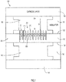
- FIG. 1 this figure illustrates a cross-sectional view of a MEMS image intensifier 100 including an electron multiplier 120 configured in accordance with an example embodiment of the present invention.
- the MEMS image intensifier 100 also includes a cathode layer 130 and a phosphor screen 140, each of which is coupled to the electron multiplier 120 via an annular insulator 150 that surrounds a vacuum gap 152.
- the electron multiplier 120 which may also be referred to as an anode 120 or gain layer 120, includes an input surface 122 and an emission surface 124 that is opposite the input surface 122.
- the cathode layer 130 sits above the input surface 122 so that the cathode layer 130 may emit electrons towards the input surface 122 (the cathode 130 and anode 120 may be collectively referred to as an electron sensing device). Meanwhile, the phosphor screen 140 sits below the emission surface 124 so that the phosphor screen 140 may receive electrons emitted from the emission surface 124.
- the cathode layer 130 may convert photons received from ambient light to electrons (e-) and release these electrons towards the electron multiplier 120.
- An electric field (not shown) between the cathode layer 130 and the electron multiplier 120 may accelerate the electrons towards the electron multiplier 120, causing the electrons to impact the electron multiplier 120.
- the electron multiplier 120 amplifies the received electrons and emits additional electrons towards the phosphor screen 140. That is, there is a gain of electrons through the electron multiplier 120.
- image intensifier 100 is merely an example and, in other embodiment, the electron multiplier 120 can be included in any MEMS image intensifiers or light detection device now known or developed hereafter.
- the particular characteristics of the electron multiplier 120 presented herein provide a highly efficient gain which, in turn, allows the image intensifier 100 (more specifically, the phosphor screen 140) to output visible light that can be viewed in a direct view system (i.e., a system where a user looks directly at phosphor for an image) or a digital system (i.e., a system where a user views a digital output from a camera focused on a phosphor screen).
- the gain layer 120 which may be formed from or on a wafer or substrate 202 (e.g., a silicon substrate), defines an active area 204 that is configured to receive and amplify electrons emitted by the cathode layer 130.
- the active area 204 includes a lattice of interior walls or ribs 210 and a series of textured surfaces 230 formed therebetween. That is, the ribs 210 form a plurality of pixels 212 and the textured surfaces 230 are formed within the pixels 212.
- the ribs 210 are made of p-type doping (i.e., formed from a doped material) and extend, at least slightly, above the input surface 122 of the gain layer 120 (which may also be referred to as the input surface 122 of the gain layer substrate 202).
- the ribs 210 also extend, at least partially through the substrate 202, in a direction that is perpendicular to the input surface 122 (as well as the output surface 124), at least in its initial state (i.e., prior to forming the textured surfaces). That is, the ribs 210 may extend orthogonally through at least a portion of the gain layer substrate 202 from the input surface 122 to or towards the emission surface 124 (which is illustrated as a vertical direction in FIG. 2 ).
- the ribs 210 can be formed in the wafer 202 with dopant selective etching techniques, implanting techniques, or any other techniques that define a lattice of doped walls or ribs 210 within and above (at least slightly) the gain layer substrate 202.
- the ribs 120 prevent, or at least discourage, electrons from moving laterally within the gain layer substrate 202 (since the doping produces an electrostatic barrier (i.e., the doping produces an electric field that repels negative charged carriers) and has a lower lifetime, it limits signal transfer).
- the textured surfaces 230 may be self-aligned on the substrate 202.
- the gain layer 120 can be etched after the ribs 210 are formed in the substrate 202 and the ribs 210 will act as a mask to ensure the etchant only etches in the pixels 212 between the ribs 210.
- the textured surfaces 230 in at least some embodiments, may be depressions that are shaped as inverted pyramids, as is described in further detail below.
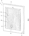
- FIG. 2 illustrates a perspective view of a die 10 including the electron multiplier 120 included in the MEMS image intensifier 100 of FIG. 1 .
- the electron multiplier 120 includes a plurality of pixels 212 that are formed, by a plurality of ribs 210, in the active area 204 (also referred to as an imagining area 204) of the die 10.
- Each pixel 212 also includes a textured surface; however, for simplicity, the textured surfaces are not shown in FIG. 2 .
- FIG. 2 provides an overall perspective of a die. Consequently, in FIG. 2 , the entire active area 204 can be clearly seen to be a square with a length and width of dimension D1.
- the active area 204 is a square area that is approximately 14 millimeters (mm) by 14 mm (i.e., D1 is 14 mm).
- the active area 204 may be any shape and size.
- the active area 204 is bounded by an external band 16 that allows the die 10 to be secured and sealed to additional components (i.e., to additional the cathode 130 and/or phosphor screen 140 with a vacuum seal).
- the external band 16 is formed from the gain layer substrate 202 (e.g., a silicon substrate).
- the pixels 212 are uniform pixels. That is, the pixels 212 are patterned in a regular, repeating pattern, insofar as the pixels 212 each have the same dimensions and are separated by the same distance.
- each pixel 212 may be a square with length and width dimensions (depicted as W1 in FIG. 4 ) in the range of approximately 4 microns to approximately 6 microns.
- each rib 210 may have a thickness (depicted as W2 in FIG. 4 ) of approximately 0.3 microns so that adjacent pixels 212 are separated by a distance of approximately 0.3 microns.
- the electron multiplier 120 may have an open area ratio of approximately 88%. That is, the pixels 212 may cover approximately 88% of the electron multiplier's normal surface area (the surface area seen from a normal position relative to the electron multiplier 120 (the top of the page in the Figures)).
- the open area ratio may be in the range of approximately 80% to 95%.
- higher open area ratios may serve to more effectively reduce the halo effect created by backscattered electrons (since higher open area ratios reduce the chance of an electron impacting a top surface 214 (see FIG. 4 ) of a rib 210), but the open area ratio must also be balanced against the structural integrity of the lattice of interior ribs 210 and the size of the pixels 212.
- thinner ribs 210 may be more unstable and larger pixels 212 may be less effective in preventing backscattered electrons from re-impacting the gain layer 120.
- the textured surfaces 230 substantially span each of the pixels 212 and, thus, the textured surfaces 230 collectively cover a portion of the active area 204 equivalent to the open area ratio (i.e., 80-95%) regardless of the particular ratio created by different configurations.
- FIG. 3 depicts in perspective the single pixel 212 from inset B of FIG. 2 , but illustrates this pixel with its textured surface 230.
- the textured surface 230 is an inverted pyramidal depression.
- the pyramid includes two sets of opposing faces: set 231 and set 233.
- the opposing sets of faces 231 and 233 form a square that spans the entire (or nearly the entire) pixel 212. That is, at the top 234, the opposing sets of faces 231 and 233 may span the four ribs 210 forming a boundary around the pixel 212.
- the four faces included in the two opposing sets of faces 231 and 233 converge at a bottom 236 of the depression 230 so that the bottom 236 is essentially a point.
- the depression 230 is formed via etching. Consequently, the depression 230 is etched along crystallographic planes and is shaped as a square pyramid. More specifically, anisotropic wet etching techniques may be utilized to etch the inverted pyramid into a Silicon wafer and, thus, the sides (e.g., the faces in sets 231 and 233) are ⁇ 111 ⁇ planes the form an interior angle between the pyramidal wall and the input surface 122 that measures 54.7° (this angle may be referred to herein as the wall angle).
- the depression the depression may take any desirable shape and may be created in any desirable manner.
- bottom 236 of the depression 230 may be a flat surface that is substantially smaller than the opening defined at the top 234 of the depression 230.
- the depression in the depicted embodiment the depression is a complete inverted pyramid, but in other embodiments, the depression 230 may be a truncated pyramid.
- the depression 230 may be a conical pyramid or any other desirable shape (e.g., to match a shape of a pixel 212 or by somehow etching along another plane).
- depressions 230 without any surfaces that are parallel to the input surface 122 may be preferred since these shapes may discourage electrons from bouncing away from the gain layer 120 (flat surfaces that are parallel to the input surface 122 may allow an electron to bounce straight away, which may allow the electron to then accelerate into another pixel).
- the depression 230 extends only partially through the substrate 202 so that holes are not formed in the gain layer 120 (which might destroy the vacuum during some of the processing steps).
- the electrons from the cathode do not have a surface to land on, the electrons from the cathode cannot create gain.
- the depth of the depression 230 is directly linked to the width W1 of the pixel 212, as governed by Pythagorean principles.
- the depth of a depression 230 may be determined by the following equation: (1 ⁇ 2 (pixel width W1) * tan(wall angle)).
- the pixel width is in the range of 4 to 6 microns (which is mentioned above as an example range)
- the depression depth may be in the range of approximately 2.8 microns to approximately 4.2 microns.
- the substrate height H2 of the ribs 210 is a non-zero height that ensures that the ribs extend at least partially through the substrate 202 (i.e., 0 ⁇ H2 ⁇ H1).
- the substrate height H2 may depend on the technique used to create the ribs 210 within the substrate 202. For example, implantation may limit the height H2 as compared to dopant selective etching techniques.
- the extension height H3 may be the height that the ribs 210 extend above a pre-textured input surface 122 (which may be aligned with a top 234 of the depressions 230).
- the extension height H3 may vary from embodiment to embodiment and may be determined by balancing the need to prevent halo effect against the need to prevent loss of electrons.
- the ribs 120 may eliminate more halo effect by preventing backscattered electrons from re-impacting different pixels 212.
- the ribs 120 may cause an increase electron loss at least because the ribs 120 may include more exposed surface area which an electron may impact (and the dopant materials forming the ribs 120 does not provide signal, so electrons impacting exposed portions of the ribs 120 may be lost).
- the rib height H3 may be determined based on pixel pitch (which may be determined based on the size of the pixels 212 and the width of the ribs 210).
- the rib height H3 may be less than approximately two-and-one-half times greater than the pixel pitch of the depressions 230 (i.e., H3 ⁇ 2.5 * pixel pitch).
- backscatter may begin to asymptote just after the wall height approaches a dimension that is 2.5 times greater than the pixel pitch and, thus, increasing the wall height H3 past this dimension (i.e., 2.5 * pixel pitch) may not be worthwhile (at least in view of the desire to minimize electron loss).
- FIG. 4 illustrates multiple possible paths (P1-P4) along which a backscattered electron may travel.
- a backscattered electron impacts the substrate 202, the electron may be captured and amplified in its proper pixel 212. If, instead, a backscattered electron impacts the doped walls 230 (or more specifically, the backscatter electron impacts an interior surface 216 of the doped walls 230), the electron may be lost.
- the backscattered electron may generate a halo effect.
- the electron may be captured and amplified.
- the electron may not generate halo effect, but it may be lost.
- the doped walls 230 should have an extension height H3 that is high enough to prevent electrons from moving between pixels 212; however, at the same time, the extension height H3 should be minimized to minimize electron loss.
- the height of the extension H3 must be determined in view of the geometry of the textured surface 230.
- the ribs 230 (or at least the portion of the ribs 230 denoted by height H3, which may be referred to as the rib extension) and the textured surfaces 230 collectively act to substantially reduce electron scatter (and the halo effect associated therewith).
- the lattice of ribs 210 prevents backscattered electrons from traveling laterally into another pixel 212 and the textured surfaces encourage backscattered electrons to bounce into the substrate or, if not, into the ribs 210. That is, the textured surfaces 230 encourage backscattering electrons to travel along path P1 or P2 or, alternatively, along path P3 or P4.
- the textured surfaces 230 encourage backscattering electrons to bounce from one face in one of the sets of faces 231, 233 towards the other face in the same set 231, 233 which, in turn, directs the backscattering electrons towards the substrate 202 or the ribs 210 bounding a pixel 212. If instead, a pixel 212 included only the ribs 210, a backscattering electron might bounce away from the gain layer in a direction normal to the input surface and escape the pixel 212. On the other hand, if a pixel 212 included only the textured surfaces 230, electrons bouncing along paths P3 or P4 would escape the pixel and degrade performance of the electron multiplier.
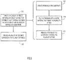
- FIG. 5 illustrates a high-level flow chart of a method for forming an electron multiplier for a MEMS image intensifier, according to an example embodiment of the present invention.
- a plurality of pixels is created.
- the plurality of pixels is created between a plurality of ribs that extend at least partially between an input surface and an emission surface of a substrate.
- the creating of the pixels at 510 is a three-step process.
- trenches are created in the substrate.
- the trenches are formed from the input surface and/or the emission surface with any techniques suitable for removing material from a semiconductor substrate (i.e., a silicon substrate); however, preferably, the trenches have a high aspect ratio (i.e., the trenches are narrow and deep). Thin trenches maximize the open area ratio of the pixels (thereby allowing the textured surfaces to cover a large portion of the input surface) while deep trenches further reduce crosstalk between pixels. Then, at 514, the trenches are filled with a doped material that forms the plurality of ribs. The doped material may be deposited in the trenches via any deposition techniques now known or developed hereafter. Finally, at 516, a portion of the substrate is removed to reveal the plurality of ribs.
- a semiconductor substrate i.e., a silicon substrate
- the trenches have a high aspect ratio (i.e., the trenches are narrow and deep). Thin trenches maximize the open area ratio of the pixels (thereby allowing the
- the substrate may be dry etched with dopant selective etching techniques to remove the substrate. This etching reveals the portion of the ribs denoted by height H3 in FIG. 4 .
- steps 512, 514, and 516 are not the only manner of creating the pixels between the plurality of ribs.
- doped ribs may be deep implanted into the substrate as an alternative to steps 512, 514, and 516.
- a plurality of textured surfaces are created in the plurality of pixels at 520.
- a substrate including the doped ribs may be wet etched to create the textured surfaces.
- the wet etching may utilize any type of silicon/bulk etchant, such as potassium hydroxide (KOH), tetra-methyl ammonium hydroxide (TMAH) and ethylene di-amine pyro-catechol (EDP). Regardless of the etchant, wet etching does not remove doped materials, so the ribs will not be removed. Instead, the ribs act as a mask so that the textured surfaces self-align (since the entire input surface can be wet etched and the textured surfaces automatically align within the pixels).
- KOH potassium hydroxide
- TMAH tetra-methyl ammonium hydroxide
- EDP ethylene di-amine pyro-catechol
- the textured surfaces will initially be formed as truncated, inverted square pyramids.
- the sides of the inverted pyramid will converge and the flat bottom of the truncated pyramid will disappear.
- the inverted pyramid may be most effective in reducing backscatter (since electrons cannot bounce off a surface that is parallel to the initial input surface of the substrate).
- an electron multiplier for a MEMS image intensifier comprising: an input surface for receiving electrons; an emission surface opposite the input surface; a plurality of doped ribs extending at least partially between the input surface and the emission surface to form a plurality of pixels; and a plurality of textured surfaces disposed in the plurality of pixels.
- a method of forming an electron multiplier for a MEMS image intensifier comprising: creating a plurality of pixels between a plurality of ribs that extend at least partially between an input surface and an emission surface of a substrate; and creating a plurality of textured surfaces in the plurality of pixels.
- an electron sensing device for a MEMS image intensifier comprising: a cathode for providing a source of electrons; and an anode for receiving electrons emitted from the cathode, the anode including a plurality of textured surfaces disposed between doped ribs that extend at least partially through the anode and define a plurality of pixels.
- the electron multiplier, method of forming the electron multiplier, and the electron sensing device presented herein provides a number of advantages. Most notably, the embodiments presented herein reduce the halo effect caused by backscattered electrons and reduces crosstalk between pixels, while also limiting the number of electrons lost between the photocathode layer or component and the electron multiplier is desired. Halo effect is reduced by the lattice of ribs that form and bound each pixel. In particular, these ribs extend above textured surfaces formed in the pixels to prevent backscattered electrons from re-impacting the gain layer at a different pixel.
- the ribs which are formed from a doped material, also extend, at least partially through the gain layer in order to prevent crosstalk between pixels in the gain layer. That is, the dopant provides lateral isolation within the gain layer. However, at the same time, the walls only extend slightly above the textured surfaces in order to minimize electron loss.
- the aforementioned features and advantages are created within the gain layer and do not require a separate layer (e.g., a separate layer of ribs) to be manufactured and bonded to the gain layer. Therefore, the techniques presented herein may be more inexpensive and less time consuming as compared to techniques that add a layer to a gain layer. In fact, the techniques herein produce a collimating structure, a doping profile, and a mask for etching of the pyramid structure (i.e., create self-aligned textured surfaces) by creating pixels defined by p-type doped ribs with a few (or a single) step process.
- the electron multiplier presented herein may be particularly inexpensive and efficient to manufacture, especially as compared to gain layers that include doped regions or textured regions that must be meticulously arranged on the gain layer. Consequently, the electron multiplier presented herein can be rapidly and efficiently produced at scale (i.e., via wafer scale processing).
- the electron multiplier presented herein reduces halo effect, crosstalk and electron loss, the electron multiplier presented herein improves image fidelity (i.e., as measured via the modulation transfer function).
- image fidelity i.e., as measured via the modulation transfer function.
- the electron multiplier presented herein may provide a performance improvement by improving the image fidelity of the image produced, regardless of whether the night vision goggles are a digital or analog solution.
- the electron multiplier presented herein is suitable for wafer scale processing, the electron multiplier may be included in an electron sensing device/ image intensifier that provides a size and weight reduction as compared to other such components.
Landscapes
- Engineering & Computer Science (AREA)
- Manufacturing & Machinery (AREA)
- Electron Tubes For Measurement (AREA)
Abstract
Description
- Image intensifiers typically include a photocathode layer or component and an electron multiplier of some type. Generally, the photocathode layer or component converts incoming photons into electrons and the electron multiplier (e.g., a photoelectric component or layer, commonly referred to as a gain layer) generates multiple electrons from electrons received from the photocathode layer or component. Often, the electron multiplier (i.e., a gain layer) utilizes electron impact ionization as a gain mechanism to amplify the electrical response generated by the photocathode layer or component (the electrical response generated in response to incoming photons).
- Unfortunately, imagers that rely on electron impact ionization as a gain mechanism often experience performance degradation when electrons move along undesirable paths prior to or subsequent to an impact. For example, if electrons backscatter (reflect or bounce) off an input surface of the electron multiplier, these backscattered electrons may create a halo effect that degrades image quality. Additionally or alternatively, some electrons, including backscattered electrons, may be lost between the photocathode layer or component and the electron multiplier (i.e., if the electrons are absorbed by a structure other than the electron multiplier). Still further, electrons may move laterally within the electron multiplier, thereby degrading the spatial fidelity of the electrons output by the electron multiplier. That is, crosstalk between pixels, or adjacent regions, in the photoelectric component or layer may cause performance degradation.
- Over time, various solutions have attempted to address at least some of these issues; however, the solutions often fail to address all three of the aforementioned issues. Moreover, the solutions may be inefficient to implement, in terms of time, resources, and cost, especially for a Micro-Electro-Mechanical-Systems (MEMS) image intensifier. For example, some electron multipliers include a collimator grid that reduces halo effect, but the collimator grid may fail to limit crosstalk between pixels of the electron multiplier and increase the amount of electrons lost between the photocathode layer and the electron multiplier. Moreover, adding a collimator grid to a substrate may be expensive and inefficient. Alternatively, some electron multipliers include textured regions while other electron multipliers include doped regions. These doped or textured regions might reduce crosstalk or halo effect, respectively, but neither of these regions addresses both issues (e.g., textured regions might reduce halo effect but do not reduce crosstalk while doped regions might reduce crosstalk without impacting halo effect). In view of the aforementioned issues, an electron multiplier that reduces the halo effect caused by backscattered electrons and reduces crosstalk between pixels, while also limiting the number of electrons lost between the photocathode layer or component and the electron multiplier is desired. In particular, an electron multiplier that provides these advantages for MEMS image intensifiers is desired.
- According to one embodiment, an electron multiplier for a Micro-Electro-Mechanical-Systems (MEMS) image intensifier includes an input surface, an emission surface, a plurality of doped ribs, and a plurality of textured surfaces. The input surface receives electrons and the emission surface is opposite the input surface. The plurality of doped ribs extends at least partially between the input surface and the emission surface to form a plurality of pixels. The plurality of textured surfaces are disposed in the plurality of pixels.
- According to another embodiment, a method of forming an electron multiplier for a MEMS image intensifier includes creating a plurality of pixels and creating a plurality of textured surfaces. The plurality of pixels are created between a plurality of ribs that extend at least partially between an input surface and an emission surface of a substrate. The plurality of textured surfaces are created in the plurality of pixels.
- According to yet another embodiment, an electron sensing device includes a cathode and an anode with a plurality of textured surfaces. The cathode provides a source of electrons and the anode receives the electrons emitted from the cathode. The plurality of textured surfaces is disposed between doped ribs. The doped ribs extend at least partially through the anode and define a plurality of pixels.
-
-
FIG. 1 illustrates a cross-sectional view of a Micro-Electro-Mechanical-Systems (MEMS) image intensifier including an electron multiplier configured in accordance with an example embodiment of the present invention. -
FIG. 2 illustrates a perspective view of the electron multiplier included in the MEMS image intensifier ofFIG. 1 . -
FIG. 3 illustrates a perspective view of inset B fromFIG. 2 . -
FIG. 4 illustrates a sectional view taken along line C-C fromFIG. 3 . This sectional view is also a close-up view of inset A from the sectional view ofFIG. 1 . -
FIG. 5 illustrates a high-level flow chart of a method for forming an electron multiplier for a MEMS image intensifier, according to an example embodiment of the present invention. - Like reference numerals have been used to identify like elements throughout this disclosure.
- An electron multiplier for a Micro-Electro-Mechanical-Systems (MEMS) image intensifier is presented herein. The electron multiplier includes ribs and textured surfaces formed between the ribs. More specifically, the electron multiplier presented herein includes p-type doped ribs that define a plurality of cells or pixels, insofar as the term "doped" or variants thereof (e.g., doping) indicates that a dopant has been added to shift the Fermi levels within the material (with p-type indicating that the ribs have been shifted to predominantly positive charge carriers). Advantageously, since the ribs are made of a p-type dopant (referred to herein simply as dopant, doping, etc.), the ribs prevent electron crosstalk between pixels. The ribs also extend above an input surface of the electron multiplier (i.e., an input surface of the gain layer) and, thus, minimize the halo effect created by backscattered electrons. Meanwhile, textured surfaces that form depressions within the plurality of pixels further assist in preventing backscattered or lost electrons.
- Typically ribs that extend above the input surface cause at least some electrons to be lost between the cathode layer and the electron multiplier (e.g., electrons impacting a top surface of a rib may be lost); however, with the electron multiplier presented herein, the textured surfaces formed between the doped ribs limit electron loss. As explained in further detail below, in at least some embodiments, the depressions are inverted pyramids formed by wet etching a substrate that includes the doped ribs. The doped ribs act as a mask when the textured surfaces are etched into the gain layer substrate. Consequently, the textured surfaces may be said to be self-aligned. By comparison, if textured or doped regions are added to a gain layer without ribs, the texturing or dopant must be meticulously applied to achieve a specific configuration.
- As mentioned, the electron multiplier presented herein is suitable for MEMS image intensifiers. As a brief example, the electron multiplier presented herein may be formed on multiple die on a wafer (e.g., 50-500 die) for an image intensifier of night vision goggles. This electron multiplier may provide performance advantages that allow a system including the electron multiplier to be substantially smaller and lighter than systems including conventional electron multipliers and, thus, may allow an image intensifier and/or a pair of night vision googles to be substantially smaller, in size and weight, than those incorporating conventional electron multipliers.
- Now turning to
FIG. 1 , this figure illustrates a cross-sectional view of aMEMS image intensifier 100 including anelectron multiplier 120 configured in accordance with an example embodiment of the present invention. TheMEMS image intensifier 100 also includes acathode layer 130 and aphosphor screen 140, each of which is coupled to theelectron multiplier 120 via anannular insulator 150 that surrounds avacuum gap 152. In particular, theelectron multiplier 120, which may also be referred to as ananode 120 orgain layer 120, includes aninput surface 122 and anemission surface 124 that is opposite theinput surface 122. Thecathode layer 130 sits above theinput surface 122 so that thecathode layer 130 may emit electrons towards the input surface 122 (thecathode 130 andanode 120 may be collectively referred to as an electron sensing device). Meanwhile, thephosphor screen 140 sits below theemission surface 124 so that thephosphor screen 140 may receive electrons emitted from theemission surface 124. - More specifically, the
cathode layer 130 may convert photons received from ambient light to electrons (e-) and release these electrons towards theelectron multiplier 120. An electric field (not shown) between thecathode layer 130 and theelectron multiplier 120 may accelerate the electrons towards theelectron multiplier 120, causing the electrons to impact theelectron multiplier 120. Theelectron multiplier 120 amplifies the received electrons and emits additional electrons towards thephosphor screen 140. That is, there is a gain of electrons through theelectron multiplier 120. However,image intensifier 100 is merely an example and, in other embodiment, theelectron multiplier 120 can be included in any MEMS image intensifiers or light detection device now known or developed hereafter. - The particular characteristics of the
electron multiplier 120 presented herein provide a highly efficient gain which, in turn, allows the image intensifier 100 (more specifically, the phosphor screen 140) to output visible light that can be viewed in a direct view system (i.e., a system where a user looks directly at phosphor for an image) or a digital system (i.e., a system where a user views a digital output from a camera focused on a phosphor screen). In particular, thegain layer 120, which may be formed from or on a wafer or substrate 202 (e.g., a silicon substrate), defines anactive area 204 that is configured to receive and amplify electrons emitted by thecathode layer 130. Theactive area 204 includes a lattice of interior walls orribs 210 and a series oftextured surfaces 230 formed therebetween. That is, theribs 210 form a plurality ofpixels 212 and thetextured surfaces 230 are formed within thepixels 212. - The
ribs 210 are made of p-type doping (i.e., formed from a doped material) and extend, at least slightly, above theinput surface 122 of the gain layer 120 (which may also be referred to as theinput surface 122 of the gain layer substrate 202). Theribs 210 also extend, at least partially through thesubstrate 202, in a direction that is perpendicular to the input surface 122 (as well as the output surface 124), at least in its initial state (i.e., prior to forming the textured surfaces). That is, theribs 210 may extend orthogonally through at least a portion of thegain layer substrate 202 from theinput surface 122 to or towards the emission surface 124 (which is illustrated as a vertical direction inFIG. 2 ). As explained in further detail below in connection withFIG. 5 , theribs 210 can be formed in thewafer 202 with dopant selective etching techniques, implanting techniques, or any other techniques that define a lattice of doped walls orribs 210 within and above (at least slightly) thegain layer substrate 202. - Notably, since the ribs arc made of a doped material, the
ribs 120 prevent, or at least discourage, electrons from moving laterally within the gain layer substrate 202 (since the doping produces an electrostatic barrier (i.e., the doping produces an electric field that repels negative charged carriers) and has a lower lifetime, it limits signal transfer). Moreover, since theribs 120 are doped, thetextured surfaces 230 may be self-aligned on thesubstrate 202. For example, if thetextured surfaces 230 are formed with wet/anisotropic etching techniques, thegain layer 120 can be etched after theribs 210 are formed in thesubstrate 202 and theribs 210 will act as a mask to ensure the etchant only etches in thepixels 212 between theribs 210. Regardless of how thetextured surfaces 230 are formed, thetextured surfaces 230, in at least some embodiments, may be depressions that are shaped as inverted pyramids, as is described in further detail below. -
FIG. 2 illustrates a perspective view of a die 10 including theelectron multiplier 120 included in theMEMS image intensifier 100 ofFIG. 1 . As mentioned, theelectron multiplier 120 includes a plurality ofpixels 212 that are formed, by a plurality ofribs 210, in the active area 204 (also referred to as an imagining area 204) of thedie 10. Eachpixel 212 also includes a textured surface; however, for simplicity, the textured surfaces are not shown inFIG. 2 . Instead,FIG. 2 provides an overall perspective of a die. Consequently, inFIG. 2 , the entireactive area 204 can be clearly seen to be a square with a length and width of dimension D1. More specifically, in the depicted example, theactive area 204 is a square area that is approximately 14 millimeters (mm) by 14 mm (i.e., D1 is 14 mm). However, in other embodiments, theactive area 204 may be any shape and size. Moreover, regardless of the shape and size of theactive area 204, theactive area 204 is bounded by anexternal band 16 that allows the die 10 to be secured and sealed to additional components (i.e., to additional thecathode 130 and/orphosphor screen 140 with a vacuum seal). In the depicted embodiment, theexternal band 16 is formed from the gain layer substrate 202 (e.g., a silicon substrate). - Still referring to
FIG. 2 , in the depicted embodiment, thepixels 212 are uniform pixels. That is, thepixels 212 are patterned in a regular, repeating pattern, insofar as thepixels 212 each have the same dimensions and are separated by the same distance. For example, eachpixel 212 may be a square with length and width dimensions (depicted as W1 inFIG. 4 ) in the range of approximately 4 microns to approximately 6 microns. Meanwhile, eachrib 210 may have a thickness (depicted as W2 inFIG. 4 ) of approximately 0.3 microns so thatadjacent pixels 212 are separated by a distance of approximately 0.3 microns. With these dimensions, theelectron multiplier 120 may have an open area ratio of approximately 88%. That is, thepixels 212 may cover approximately 88% of the electron multiplier's normal surface area (the surface area seen from a normal position relative to the electron multiplier 120 (the top of the page in the Figures)). - However, in other embodiments, the open area ratio may be in the range of approximately 80% to 95%. Generally, higher open area ratios may serve to more effectively reduce the halo effect created by backscattered electrons (since higher open area ratios reduce the chance of an electron impacting a top surface 214 (see
FIG. 4 ) of a rib 210), but the open area ratio must also be balanced against the structural integrity of the lattice ofinterior ribs 210 and the size of thepixels 212. Notably,thinner ribs 210 may be more unstable andlarger pixels 212 may be less effective in preventing backscattered electrons from re-impacting thegain layer 120. As is explained in further detail below, thetextured surfaces 230 substantially span each of thepixels 212 and, thus, thetextured surfaces 230 collectively cover a portion of theactive area 204 equivalent to the open area ratio (i.e., 80-95%) regardless of the particular ratio created by different configurations. -
FIG. 3 depicts in perspective thesingle pixel 212 from inset B ofFIG. 2 , but illustrates this pixel with itstextured surface 230. As can be seen, in the depicted embodiment, thetextured surface 230 is an inverted pyramidal depression. The pyramid includes two sets of opposing faces: set 231 and set 233. At a top 234 of thedepression 230, the opposing sets offaces pixel 212. That is, at the top 234, the opposing sets offaces ribs 210 forming a boundary around thepixel 212. Meanwhile, the four faces included in the two opposing sets offaces depression 230 so that the bottom 236 is essentially a point. - As is explained in further detail below in connection with
FIG. 5 , in the depicted embodiment, thedepression 230 is formed via etching. Consequently, thedepression 230 is etched along crystallographic planes and is shaped as a square pyramid. More specifically, anisotropic wet etching techniques may be utilized to etch the inverted pyramid into a Silicon wafer and, thus, the sides (e.g., the faces insets 231 and 233) are {111} planes the form an interior angle between the pyramidal wall and theinput surface 122 that measures 54.7° (this angle may be referred to herein as the wall angle). - That being said, in different embodiments, the depression the depression may take any desirable shape and may be created in any desirable manner. For example,
bottom 236 of thedepression 230 may be a flat surface that is substantially smaller than the opening defined at the top 234 of thedepression 230. In other words, in the depicted embodiment the depression is a complete inverted pyramid, but in other embodiments, thedepression 230 may be a truncated pyramid. In still other embodiments, thedepression 230 may be a conical pyramid or any other desirable shape (e.g., to match a shape of apixel 212 or by somehow etching along another plane). However,depressions 230 without any surfaces that are parallel to the input surface 122 (e.g., complete pyramids) may be preferred since these shapes may discourage electrons from bouncing away from the gain layer 120 (flat surfaces that are parallel to theinput surface 122 may allow an electron to bounce straight away, which may allow the electron to then accelerate into another pixel). Moreover, regardless of its shape, thedepression 230 extends only partially through thesubstrate 202 so that holes are not formed in the gain layer 120 (which might destroy the vacuum during some of the processing steps). Notably , if the electrons from the cathode do not have a surface to land on, the electrons from the cathode cannot create gain. - Still referring to
FIG. 3 , but now with reference toFIG.4 as well (which illustrates sectional view of a pixel taken along line C-C fromFIG. 3 that is also a close-up view of inset A fromFIG. 1 ), in the depicted embodiment, the depth of thedepression 230 is directly linked to the width W1 of thepixel 212, as governed by Pythagorean principles. In particular, the depth of adepression 230 may be determined by the following equation: (½ (pixel width W1) * tan(wall angle)). Thus, if anisotropic wet etching techniques are utilized to etch the inverted pyramid into a silicon wafer (and, thus, the wall angle is 54.7°), the depression depth may be approximately 7/10 the size of the pixel width (i.e., tan(54.7°)*0.5 = approximately 0.7). As a specific example, if the pixel width is in the range of 4 to 6 microns (which is mentioned above as an example range), the depression depth may be in the range of approximately 2.8 microns to approximately 4.2 microns. These formulas may hold true even if the etching somehow acts along a different plane, but will not hold true if the etching somehow creates curvature in the depression walls. - By comparison, and now referring to
FIG. 4 , the height of theribs 230 may be loosely tied to the size of thepixels 212, but may not be directly determinable based on the pixel size. Instead, the overall height of theribs 212 may be the sum of a substrate height H2 and an extension height H3 (i.e., H2 + H3 = the overall height of the ribs 210), each of which may be determined based on distinct factors. First, the substrate height H2 of theribs 210 is a non-zero height that ensures that the ribs extend at least partially through the substrate 202 (i.e., 0 < H2 ≤ H1). However, at the same time, theribs 210 may be more effective at limiting crosstalk between pixels as H2 converges on H1. That is,ribs 210 that extend further through thesubstrate 202 may be more effective at eliminating crosstalk betweenpixels 212. Consequently, in at least some embodiments, the substrate height H2 may be based on the height H1 of the substrate. In fact, in some embodiments, the ribs may extend entirely through the substrate 202 (and, thus, H2=H1). Alternatively, theribs 210 may have a substrate height H2 that is a fraction of the height H1 of the substrate. For example, theribs 210 may extend halfway or three-quarters of the way through the substrate (i.e., H2 = 0.5*H1 or 0.75*H1). However, generally, the substrate height H2 may depend on the technique used to create theribs 210 within thesubstrate 202. For example, implantation may limit the height H2 as compared to dopant selective etching techniques. - Second, the extension height H3 may be the height that the
ribs 210 extend above a pre-textured input surface 122 (which may be aligned with a top 234 of the depressions 230). The extension height H3 may vary from embodiment to embodiment and may be determined by balancing the need to prevent halo effect against the need to prevent loss of electrons. Notably, if the ribs include a height H3 that is relatively taller (i.e., as the ribs extend further above the input surface 122), theribs 120 may eliminate more halo effect by preventing backscattered electrons from re-impactingdifferent pixels 212. However, as theribs 120 extend further above the input surface 122 (i.e., as H3 increases), theribs 120 may cause an increase electron loss at least because theribs 120 may include more exposed surface area which an electron may impact (and the dopant materials forming theribs 120 does not provide signal, so electrons impacting exposed portions of theribs 120 may be lost). - In at least some embodiments, the rib height H3 may be determined based on pixel pitch (which may be determined based on the size of the
pixels 212 and the width of the ribs 210). For example, the rib height H3 may be less than approximately two-and-one-half times greater than the pixel pitch of the depressions 230 (i.e., H3 < 2.5 * pixel pitch). Notably, backscatter may begin to asymptote just after the wall height approaches a dimension that is 2.5 times greater than the pixel pitch and, thus, increasing the wall height H3 past this dimension (i.e., 2.5 * pixel pitch) may not be worthwhile (at least in view of the desire to minimize electron loss). As an example, when thepixels 212 are squares with length and width dimensions in the range of approximately 4 to approximately 6 microns, theribs 210 may have a height H3 that is less than approximately 10 to approximately 15 microns (as determined by multiplying the specific length/width dimension by 2.5). As a more specific example, theribs 210 may extend approximately 5 to approximately 10 microns above the input surface (i.e., H3 = 5-10 microns) when thepixels 212 are squares with length and width dimensions in the range of approximately 4 to approximately 6 microns. At this height, theribs 120 may reduce the halo effect without providing a substantial increase in lost electrons. - To demonstrate the interplay between the extension height H3, halo effect, and electron loss,
FIG. 4 illustrates multiple possible paths (P1-P4) along which a backscattered electron may travel. Notably, if a backscattered electron impacts thesubstrate 202, the electron may be captured and amplified in itsproper pixel 212. If, instead, a backscattered electron impacts the doped walls 230 (or more specifically, the backscatter electron impacts aninterior surface 216 of the doped walls 230), the electron may be lost. Still further, if a backscattered electron travels into another pixel 212 (i.e., a backscattered electron travels above thetop surface 214 of the dopedwalls 230 and into another pixel 212), the backscattered electron may generate a halo effect. Thus, inFIG. 4 , if the electron travels along path P3 or P4, the electron may be captured and amplified. Alternatively, if the electron travels along path P2 or P1, the electron may not generate halo effect, but it may be lost. Thus, the dopedwalls 230 should have an extension height H3 that is high enough to prevent electrons from moving betweenpixels 212; however, at the same time, the extension height H3 should be minimized to minimize electron loss. Moreover, the height of the extension H3 must be determined in view of the geometry of thetextured surface 230. - Regardless of the specific height H3 of the
ribs 210, the ribs 230 (or at least the portion of theribs 230 denoted by height H3, which may be referred to as the rib extension) and thetextured surfaces 230 collectively act to substantially reduce electron scatter (and the halo effect associated therewith). In particular, the lattice ofribs 210 prevents backscattered electrons from traveling laterally into anotherpixel 212 and the textured surfaces encourage backscattered electrons to bounce into the substrate or, if not, into theribs 210. That is, thetextured surfaces 230 encourage backscattering electrons to travel along path P1 or P2 or, alternatively, along path P3 or P4. Put another way, thetextured surfaces 230 encourage backscattering electrons to bounce from one face in one of the sets offaces same set substrate 202 or theribs 210 bounding apixel 212. If instead, apixel 212 included only theribs 210, a backscattering electron might bounce away from the gain layer in a direction normal to the input surface and escape thepixel 212. On the other hand, if apixel 212 included only thetextured surfaces 230, electrons bouncing along paths P3 or P4 would escape the pixel and degrade performance of the electron multiplier. -
FIG. 5 illustrates a high-level flow chart of a method for forming an electron multiplier for a MEMS image intensifier, according to an example embodiment of the present invention. Initially, atstep 510, a plurality of pixels is created. The plurality of pixels is created between a plurality of ribs that extend at least partially between an input surface and an emission surface of a substrate. In at least one embodiment, the creating of the pixels at 510 is a three-step process. First, at 512, trenches are created in the substrate. The trenches are formed from the input surface and/or the emission surface with any techniques suitable for removing material from a semiconductor substrate (i.e., a silicon substrate); however, preferably, the trenches have a high aspect ratio (i.e., the trenches are narrow and deep). Thin trenches maximize the open area ratio of the pixels (thereby allowing the textured surfaces to cover a large portion of the input surface) while deep trenches further reduce crosstalk between pixels. Then, at 514, the trenches are filled with a doped material that forms the plurality of ribs. The doped material may be deposited in the trenches via any deposition techniques now known or developed hereafter. Finally, at 516, a portion of the substrate is removed to reveal the plurality of ribs. For example, the substrate may be dry etched with dopant selective etching techniques to remove the substrate. This etching reveals the portion of the ribs denoted by height H3 inFIG. 4 . However, steps 512, 514, and 516 are not the only manner of creating the pixels between the plurality of ribs. For example, in some embodiments, doped ribs may be deep implanted into the substrate as an alternative tosteps - Once the plurality of pixels are created, a plurality of textured surfaces are created in the plurality of pixels at 520. For example, a substrate including the doped ribs may be wet etched to create the textured surfaces. The wet etching may utilize any type of silicon/bulk etchant, such as potassium hydroxide (KOH), tetra-methyl ammonium hydroxide (TMAH) and ethylene di-amine pyro-catechol (EDP). Regardless of the etchant, wet etching does not remove doped materials, so the ribs will not be removed. Instead, the ribs act as a mask so that the textured surfaces self-align (since the entire input surface can be wet etched and the textured surfaces automatically align within the pixels). Notably, with wet etching, the textured surfaces will initially be formed as truncated, inverted square pyramids. However, as the wet etching continues, the sides of the inverted pyramid will converge and the flat bottom of the truncated pyramid will disappear. As mentioned, the inverted pyramid may be most effective in reducing backscatter (since electrons cannot bounce off a surface that is parallel to the initial input surface of the substrate).
- To summarize, in one form, an electron multiplier for a MEMS image intensifier is provided, comprising: an input surface for receiving electrons; an emission surface opposite the input surface; a plurality of doped ribs extending at least partially between the input surface and the emission surface to form a plurality of pixels; and a plurality of textured surfaces disposed in the plurality of pixels.
- In another form, a method of forming an electron multiplier for a MEMS image intensifier is provided, comprising: creating a plurality of pixels between a plurality of ribs that extend at least partially between an input surface and an emission surface of a substrate; and creating a plurality of textured surfaces in the plurality of pixels.
- In yet another form, an electron sensing device for a MEMS image intensifier is provided, comprising: a cathode for providing a source of electrons; and an anode for receiving electrons emitted from the cathode, the anode including a plurality of textured surfaces disposed between doped ribs that extend at least partially through the anode and define a plurality of pixels.
- The electron multiplier, method of forming the electron multiplier, and the electron sensing device presented herein provides a number of advantages. Most notably, the embodiments presented herein reduce the halo effect caused by backscattered electrons and reduces crosstalk between pixels, while also limiting the number of electrons lost between the photocathode layer or component and the electron multiplier is desired. Halo effect is reduced by the lattice of ribs that form and bound each pixel. In particular, these ribs extend above textured surfaces formed in the pixels to prevent backscattered electrons from re-impacting the gain layer at a different pixel. The ribs, which are formed from a doped material, also extend, at least partially through the gain layer in order to prevent crosstalk between pixels in the gain layer. That is, the dopant provides lateral isolation within the gain layer. However, at the same time, the walls only extend slightly above the textured surfaces in order to minimize electron loss.
- Moreover, the aforementioned features and advantages are created within the gain layer and do not require a separate layer (e.g., a separate layer of ribs) to be manufactured and bonded to the gain layer. Therefore, the techniques presented herein may be more inexpensive and less time consuming as compared to techniques that add a layer to a gain layer. In fact, the techniques herein produce a collimating structure, a doping profile, and a mask for etching of the pyramid structure (i.e., create self-aligned textured surfaces) by creating pixels defined by p-type doped ribs with a few (or a single) step process. Thus, the electron multiplier presented herein may be particularly inexpensive and efficient to manufacture, especially as compared to gain layers that include doped regions or textured regions that must be meticulously arranged on the gain layer. Consequently, the electron multiplier presented herein can be rapidly and efficiently produced at scale (i.e., via wafer scale processing).
- At a higher level, since the electron multiplier presented herein reduces halo effect, crosstalk and electron loss, the electron multiplier presented herein improves image fidelity (i.e., as measured via the modulation transfer function). Thus, when the electron multiplier presented herein is incorporated into various imaging products, such as night vision goggles or scopes, the electron multiplier may provide a performance improvement by improving the image fidelity of the image produced, regardless of whether the night vision goggles are a digital or analog solution. Moreover, since the electron multiplier presented herein is suitable for wafer scale processing, the electron multiplier may be included in an electron sensing device/ image intensifier that provides a size and weight reduction as compared to other such components.
- It is to be understood that terms such as "left," "right," "top," "bottom," "front," "rear," "side," "height," "length," "width," "upper," "lower," "interior," "exterior," "inner," "outer" and the like as may be used herein, merely describe points or portions of reference and do not limit the present invention to any particular orientation or configuration. Further, the term "exemplary" is used herein to describe an example or illustration. Any embodiment described herein as exemplary is not to be construed as a preferred or advantageous embodiment, but rather as one example or illustration of a possible embodiment of the invention.
- Although the disclosed inventions are illustrated and described herein as embodied in one or more specific examples, it is nevertheless not intended to be limited to the details shown, since various modifications and structural changes may be made therein without departing from the scope of the inventions and within the scope and range of equivalents of the claims. In addition, various features from one of the embodiments may be incorporated into another of the embodiments. Accordingly, it is appropriate that the appended claims be construed broadly and in a manner consistent with the scope of the disclosure as set forth in the following claims.
Claims (10)
- An electron multiplier apparatus comprising:an input surface for receiving electrons;an emission surface opposite the input surface;a plurality of doped ribs extending at least partially between the input surface and the emission surface to form a plurality of pixels; anda plurality of textured surfaces disposed in the plurality of pixels.
- The electron multiplier apparatus of claim 1, wherein the plurality of textured surfaces comprise a plurality of depressions.
- The electron multiplier apparatus of claim 2, wherein each of the plurality of depressions is an inverted pyramid.
- The electron multiplier apparatus of claim 3, wherein the inverted pyramid includes two sets of opposing faces and the two sets of opposing faces meet at a point at a bottom of the depression.
- The electron multiplier apparatus of claim 1, wherein the plurality of doped ribs extend above the input surface.
- The electron multiplier apparatus of claim 1, wherein the plurality of pixels are square pixels and the plurality of textured surfaces include tops defined by the square pixels.
- A method of forming an electron multiplier for a Micro-Electro-Mechanical-Systems (MEMS) image intensifier, comprising:creating a plurality of pixels between a plurality of ribs that extend at least partially between an input surface and an emission surface of a substrate; andcreating a plurality of textured surfaces in the plurality of pixels.
- The method of claim 7, wherein the creating of the plurality of pixels comprises:creating trenches in the substrate;filling the trenches with a doped material that forms the plurality of ribs; andremoving a portion of the substrate to reveal the plurality of ribs.
- The method of claim 7, wherein the creating the plurality of textured surfaces comprises:wet etching the substrate between the plurality of ribs to form the textured surfaces in the pixels.
- The method of claim 9, wherein the plurality of ribs are formed from a doped material and act as a mask during the wet etching.
Priority Applications (1)
| Application Number | Priority Date | Filing Date | Title |
|---|---|---|---|
| EP19150940.5A EP3680928B1 (en) | 2019-01-09 | 2019-01-09 | Electron multiplier for mems light detection device |
Applications Claiming Priority (1)
| Application Number | Priority Date | Filing Date | Title |
|---|---|---|---|
| EP19150940.5A EP3680928B1 (en) | 2019-01-09 | 2019-01-09 | Electron multiplier for mems light detection device |
Publications (2)
| Publication Number | Publication Date |
|---|---|
| EP3680928A1 true EP3680928A1 (en) | 2020-07-15 |
| EP3680928B1 EP3680928B1 (en) | 2021-08-25 |
Family
ID=65023713
Family Applications (1)
| Application Number | Title | Priority Date | Filing Date |
|---|---|---|---|
| EP19150940.5A Active EP3680928B1 (en) | 2019-01-09 | 2019-01-09 | Electron multiplier for mems light detection device |
Country Status (1)
| Country | Link |
|---|---|
| EP (1) | EP3680928B1 (en) |
Citations (2)
| Publication number | Priority date | Publication date | Assignee | Title |
|---|---|---|---|---|
| US20050122021A1 (en) * | 2003-12-03 | 2005-06-09 | Smith Arlynn W. | Surface structures for halo reduction in electron bombarded devices |
| US10312047B1 (en) * | 2018-06-01 | 2019-06-04 | Eagle Technology, Llc | Passive local area saturation of electron bombarded gain |
-
2019
- 2019-01-09 EP EP19150940.5A patent/EP3680928B1/en active Active
Patent Citations (2)
| Publication number | Priority date | Publication date | Assignee | Title |
|---|---|---|---|---|
| US20050122021A1 (en) * | 2003-12-03 | 2005-06-09 | Smith Arlynn W. | Surface structures for halo reduction in electron bombarded devices |
| US10312047B1 (en) * | 2018-06-01 | 2019-06-04 | Eagle Technology, Llc | Passive local area saturation of electron bombarded gain |
Also Published As
| Publication number | Publication date |
|---|---|
| EP3680928B1 (en) | 2021-08-25 |
Similar Documents
| Publication | Publication Date | Title |
|---|---|---|
| CN1890773B (en) | Surface structures for halo reduction in electron bombarded devices | |
| US8440495B2 (en) | Method for reducing crosstalk in image sensors using implant technology | |
| US10930700B2 (en) | Semiconductor light detection element | |
| US10163599B1 (en) | Electron multiplier for MEMs light detection device | |
| JP6688928B2 (en) | Passive local region saturation of electron impact gain | |
| US8618498B2 (en) | Backscatter reduction in thin electron detectors | |
| EP3680928B1 (en) | Electron multiplier for mems light detection device | |
| JP4976277B2 (en) | Solid image device with thinned back | |
| US6836059B2 (en) | Image intensifier and electron multiplier therefor | |
| EP3576127A1 (en) | Image intensifier with stray particle shield | |
| JP2025142052A (en) | Microchannel plate and method for manufacturing microchannel plate selectively formed on one side of channel opening and having metal contact | |
| JP7218437B2 (en) | Scintillator for charged particle beam equipment and charged particle beam equipment | |
| EP3987561B1 (en) | Image intensifier with thin layer transmission layer support structures | |
| EP3350825B1 (en) | A phototube and method of making it | |
| JP6532589B1 (en) | Micro-electro-mechanical device | |
| EP3492961B1 (en) | Phosphor screen for mems image intensifiers | |
| EP1652237B1 (en) | Backside thinning of image array devices | |
| US20240204127A1 (en) | Avalanche photodiode | |
| CN119008353B (en) | Electron bombardment photodetector unit and array with charge collection function | |
| CN114287060A (en) | Pixel structure and manufacturing method thereof | |
| WO2023092819A1 (en) | Fin semiconductor device and preparation method therefor | |
| JP2007180092A (en) | Imaging device | |
| JP2008097971A (en) | Imaging device |
Legal Events
| Date | Code | Title | Description |
|---|---|---|---|
| PUAI | Public reference made under article 153(3) epc to a published international application that has entered the european phase |
Free format text: ORIGINAL CODE: 0009012 |
|
| STAA | Information on the status of an ep patent application or granted ep patent |
Free format text: STATUS: REQUEST FOR EXAMINATION WAS MADE |
|
| 17P | Request for examination filed |
Effective date: 20190109 |
|
| AK | Designated contracting states |
Kind code of ref document: A1 Designated state(s): AL AT BE BG CH CY CZ DE DK EE ES FI FR GB GR HR HU IE IS IT LI LT LU LV MC MK MT NL NO PL PT RO RS SE SI SK SM TR |
|
| AX | Request for extension of the european patent |
Extension state: BA ME |
|
| GRAP | Despatch of communication of intention to grant a patent |
Free format text: ORIGINAL CODE: EPIDOSNIGR1 |
|
| STAA | Information on the status of an ep patent application or granted ep patent |
Free format text: STATUS: GRANT OF PATENT IS INTENDED |
|
| RIC1 | Information provided on ipc code assigned before grant |
Ipc: G02B 23/12 20060101ALN20210226BHEP Ipc: H01J 9/12 20060101ALI20210226BHEP Ipc: H01J 1/34 20060101AFI20210226BHEP |
|
| INTG | Intention to grant announced |
Effective date: 20210324 |
|
| RIN1 | Information on inventor provided before grant (corrected) |
Inventor name: CHILCOTT, DAN Inventor name: SMITH, ARLYNN W. |
|
| GRAS | Grant fee paid |
Free format text: ORIGINAL CODE: EPIDOSNIGR3 |
|
| GRAA | (expected) grant |
Free format text: ORIGINAL CODE: 0009210 |
|
| STAA | Information on the status of an ep patent application or granted ep patent |
Free format text: STATUS: THE PATENT HAS BEEN GRANTED |
|
| AK | Designated contracting states |
Kind code of ref document: B1 Designated state(s): AL AT BE BG CH CY CZ DE DK EE ES FI FR GB GR HR HU IE IS IT LI LT LU LV MC MK MT NL NO PL PT RO RS SE SI SK SM TR |
|
| REG | Reference to a national code |
Ref country code: CH Ref legal event code: EP |
|
| REG | Reference to a national code |
Ref country code: DE Ref legal event code: R096 Ref document number: 602019007027 Country of ref document: DE |
|
| REG | Reference to a national code |
Ref country code: NL Ref legal event code: FP Ref country code: IE Ref legal event code: FG4D Ref country code: AT Ref legal event code: REF Ref document number: 1424664 Country of ref document: AT Kind code of ref document: T Effective date: 20210915 |
|
| REG | Reference to a national code |
Ref country code: LT Ref legal event code: MG9D |
|
| REG | Reference to a national code |
Ref country code: AT Ref legal event code: MK05 Ref document number: 1424664 Country of ref document: AT Kind code of ref document: T Effective date: 20210825 |
|
| PG25 | Lapsed in a contracting state [announced via postgrant information from national office to epo] |
Ref country code: RS Free format text: LAPSE BECAUSE OF FAILURE TO SUBMIT A TRANSLATION OF THE DESCRIPTION OR TO PAY THE FEE WITHIN THE PRESCRIBED TIME-LIMIT Effective date: 20210825 Ref country code: SE Free format text: LAPSE BECAUSE OF FAILURE TO SUBMIT A TRANSLATION OF THE DESCRIPTION OR TO PAY THE FEE WITHIN THE PRESCRIBED TIME-LIMIT Effective date: 20210825 Ref country code: FI Free format text: LAPSE BECAUSE OF FAILURE TO SUBMIT A TRANSLATION OF THE DESCRIPTION OR TO PAY THE FEE WITHIN THE PRESCRIBED TIME-LIMIT Effective date: 20210825 Ref country code: ES Free format text: LAPSE BECAUSE OF FAILURE TO SUBMIT A TRANSLATION OF THE DESCRIPTION OR TO PAY THE FEE WITHIN THE PRESCRIBED TIME-LIMIT Effective date: 20210825 Ref country code: LT Free format text: LAPSE BECAUSE OF FAILURE TO SUBMIT A TRANSLATION OF THE DESCRIPTION OR TO PAY THE FEE WITHIN THE PRESCRIBED TIME-LIMIT Effective date: 20210825 Ref country code: BG Free format text: LAPSE BECAUSE OF FAILURE TO SUBMIT A TRANSLATION OF THE DESCRIPTION OR TO PAY THE FEE WITHIN THE PRESCRIBED TIME-LIMIT Effective date: 20211125 Ref country code: AT Free format text: LAPSE BECAUSE OF FAILURE TO SUBMIT A TRANSLATION OF THE DESCRIPTION OR TO PAY THE FEE WITHIN THE PRESCRIBED TIME-LIMIT Effective date: 20210825 Ref country code: HR Free format text: LAPSE BECAUSE OF FAILURE TO SUBMIT A TRANSLATION OF THE DESCRIPTION OR TO PAY THE FEE WITHIN THE PRESCRIBED TIME-LIMIT Effective date: 20210825 Ref country code: NO Free format text: LAPSE BECAUSE OF FAILURE TO SUBMIT A TRANSLATION OF THE DESCRIPTION OR TO PAY THE FEE WITHIN THE PRESCRIBED TIME-LIMIT Effective date: 20211125 Ref country code: PT Free format text: LAPSE BECAUSE OF FAILURE TO SUBMIT A TRANSLATION OF THE DESCRIPTION OR TO PAY THE FEE WITHIN THE PRESCRIBED TIME-LIMIT Effective date: 20211227 |
|
| PG25 | Lapsed in a contracting state [announced via postgrant information from national office to epo] |
Ref country code: PL Free format text: LAPSE BECAUSE OF FAILURE TO SUBMIT A TRANSLATION OF THE DESCRIPTION OR TO PAY THE FEE WITHIN THE PRESCRIBED TIME-LIMIT Effective date: 20210825 Ref country code: LV Free format text: LAPSE BECAUSE OF FAILURE TO SUBMIT A TRANSLATION OF THE DESCRIPTION OR TO PAY THE FEE WITHIN THE PRESCRIBED TIME-LIMIT Effective date: 20210825 Ref country code: GR Free format text: LAPSE BECAUSE OF FAILURE TO SUBMIT A TRANSLATION OF THE DESCRIPTION OR TO PAY THE FEE WITHIN THE PRESCRIBED TIME-LIMIT Effective date: 20211126 |
|
| PG25 | Lapsed in a contracting state [announced via postgrant information from national office to epo] |
Ref country code: DK Free format text: LAPSE BECAUSE OF FAILURE TO SUBMIT A TRANSLATION OF THE DESCRIPTION OR TO PAY THE FEE WITHIN THE PRESCRIBED TIME-LIMIT Effective date: 20210825 |
|
| REG | Reference to a national code |
Ref country code: DE Ref legal event code: R097 Ref document number: 602019007027 Country of ref document: DE |
|
| PG25 | Lapsed in a contracting state [announced via postgrant information from national office to epo] |
Ref country code: SM Free format text: LAPSE BECAUSE OF FAILURE TO SUBMIT A TRANSLATION OF THE DESCRIPTION OR TO PAY THE FEE WITHIN THE PRESCRIBED TIME-LIMIT Effective date: 20210825 Ref country code: SK Free format text: LAPSE BECAUSE OF FAILURE TO SUBMIT A TRANSLATION OF THE DESCRIPTION OR TO PAY THE FEE WITHIN THE PRESCRIBED TIME-LIMIT Effective date: 20210825 Ref country code: RO Free format text: LAPSE BECAUSE OF FAILURE TO SUBMIT A TRANSLATION OF THE DESCRIPTION OR TO PAY THE FEE WITHIN THE PRESCRIBED TIME-LIMIT Effective date: 20210825 Ref country code: EE Free format text: LAPSE BECAUSE OF FAILURE TO SUBMIT A TRANSLATION OF THE DESCRIPTION OR TO PAY THE FEE WITHIN THE PRESCRIBED TIME-LIMIT Effective date: 20210825 Ref country code: CZ Free format text: LAPSE BECAUSE OF FAILURE TO SUBMIT A TRANSLATION OF THE DESCRIPTION OR TO PAY THE FEE WITHIN THE PRESCRIBED TIME-LIMIT Effective date: 20210825 Ref country code: AL Free format text: LAPSE BECAUSE OF FAILURE TO SUBMIT A TRANSLATION OF THE DESCRIPTION OR TO PAY THE FEE WITHIN THE PRESCRIBED TIME-LIMIT Effective date: 20210825 |
|
| PLBE | No opposition filed within time limit |
Free format text: ORIGINAL CODE: 0009261 |
|
| STAA | Information on the status of an ep patent application or granted ep patent |
Free format text: STATUS: NO OPPOSITION FILED WITHIN TIME LIMIT |
|
| PG25 | Lapsed in a contracting state [announced via postgrant information from national office to epo] |
Ref country code: IT Free format text: LAPSE BECAUSE OF FAILURE TO SUBMIT A TRANSLATION OF THE DESCRIPTION OR TO PAY THE FEE WITHIN THE PRESCRIBED TIME-LIMIT Effective date: 20210825 |
|
| 26N | No opposition filed |
Effective date: 20220527 |
|
| PG25 | Lapsed in a contracting state [announced via postgrant information from national office to epo] |
Ref country code: SI Free format text: LAPSE BECAUSE OF FAILURE TO SUBMIT A TRANSLATION OF THE DESCRIPTION OR TO PAY THE FEE WITHIN THE PRESCRIBED TIME-LIMIT Effective date: 20210825 Ref country code: MC Free format text: LAPSE BECAUSE OF FAILURE TO SUBMIT A TRANSLATION OF THE DESCRIPTION OR TO PAY THE FEE WITHIN THE PRESCRIBED TIME-LIMIT Effective date: 20210825 |
|
| REG | Reference to a national code |
Ref country code: CH Ref legal event code: PL |
|
| REG | Reference to a national code |
Ref country code: BE Ref legal event code: MM Effective date: 20220131 |
|
| PG25 | Lapsed in a contracting state [announced via postgrant information from national office to epo] |
Ref country code: LU Free format text: LAPSE BECAUSE OF NON-PAYMENT OF DUE FEES Effective date: 20220109 |
|
| PG25 | Lapsed in a contracting state [announced via postgrant information from national office to epo] |
Ref country code: BE Free format text: LAPSE BECAUSE OF NON-PAYMENT OF DUE FEES Effective date: 20220131 |
|
| PG25 | Lapsed in a contracting state [announced via postgrant information from national office to epo] |
Ref country code: LI Free format text: LAPSE BECAUSE OF NON-PAYMENT OF DUE FEES Effective date: 20220131 Ref country code: CH Free format text: LAPSE BECAUSE OF NON-PAYMENT OF DUE FEES Effective date: 20220131 |
|
| PG25 | Lapsed in a contracting state [announced via postgrant information from national office to epo] |
Ref country code: IE Free format text: LAPSE BECAUSE OF NON-PAYMENT OF DUE FEES Effective date: 20220109 |
|
| P01 | Opt-out of the competence of the unified patent court (upc) registered |
Effective date: 20230627 |
|
| GBPC | Gb: european patent ceased through non-payment of renewal fee |
Effective date: 20230109 |
|
| PG25 | Lapsed in a contracting state [announced via postgrant information from national office to epo] |
Ref country code: GB Free format text: LAPSE BECAUSE OF NON-PAYMENT OF DUE FEES Effective date: 20230109 |
|
| PG25 | Lapsed in a contracting state [announced via postgrant information from national office to epo] |
Ref country code: MK Free format text: LAPSE BECAUSE OF FAILURE TO SUBMIT A TRANSLATION OF THE DESCRIPTION OR TO PAY THE FEE WITHIN THE PRESCRIBED TIME-LIMIT Effective date: 20210825 Ref country code: CY Free format text: LAPSE BECAUSE OF FAILURE TO SUBMIT A TRANSLATION OF THE DESCRIPTION OR TO PAY THE FEE WITHIN THE PRESCRIBED TIME-LIMIT Effective date: 20210825 |
|
| PG25 | Lapsed in a contracting state [announced via postgrant information from national office to epo] |
Ref country code: HU Free format text: LAPSE BECAUSE OF FAILURE TO SUBMIT A TRANSLATION OF THE DESCRIPTION OR TO PAY THE FEE WITHIN THE PRESCRIBED TIME-LIMIT; INVALID AB INITIO Effective date: 20190109 |
|
| PG25 | Lapsed in a contracting state [announced via postgrant information from national office to epo] |
Ref country code: MT Free format text: LAPSE BECAUSE OF FAILURE TO SUBMIT A TRANSLATION OF THE DESCRIPTION OR TO PAY THE FEE WITHIN THE PRESCRIBED TIME-LIMIT Effective date: 20210825 |
|
| PG25 | Lapsed in a contracting state [announced via postgrant information from national office to epo] |
Ref country code: TR Free format text: LAPSE BECAUSE OF FAILURE TO SUBMIT A TRANSLATION OF THE DESCRIPTION OR TO PAY THE FEE WITHIN THE PRESCRIBED TIME-LIMIT Effective date: 20210825 |
|
| PGFP | Annual fee paid to national office [announced via postgrant information from national office to epo] |
Ref country code: NL Payment date: 20260121 Year of fee payment: 8 |
|
| PGFP | Annual fee paid to national office [announced via postgrant information from national office to epo] |
Ref country code: DE Payment date: 20260120 Year of fee payment: 8 |
|
| PGFP | Annual fee paid to national office [announced via postgrant information from national office to epo] |
Ref country code: FR Payment date: 20260121 Year of fee payment: 8 |