EP3680633A1 - Optical power detection device and apparatus - Google Patents
Optical power detection device and apparatus Download PDFInfo
- Publication number
- EP3680633A1 EP3680633A1 EP18853370.7A EP18853370A EP3680633A1 EP 3680633 A1 EP3680633 A1 EP 3680633A1 EP 18853370 A EP18853370 A EP 18853370A EP 3680633 A1 EP3680633 A1 EP 3680633A1
- Authority
- EP
- European Patent Office
- Prior art keywords
- optical
- optical power
- signal
- power detection
- detection device
- Prior art date
- Legal status (The legal status is an assumption and is not a legal conclusion. Google has not performed a legal analysis and makes no representation as to the accuracy of the status listed.)
- Granted
Links
Images



Classifications
-
- G—PHYSICS
- G01—MEASURING; TESTING
- G01J—MEASUREMENT OF INTENSITY, VELOCITY, SPECTRAL CONTENT, POLARISATION, PHASE OR PULSE CHARACTERISTICS OF INFRARED, VISIBLE OR ULTRAVIOLET LIGHT; COLORIMETRY; RADIATION PYROMETRY
- G01J1/00—Photometry, e.g. photographic exposure meter
- G01J1/42—Photometry, e.g. photographic exposure meter using electric radiation detectors
- G01J1/44—Electric circuits
-
- G—PHYSICS
- G01—MEASURING; TESTING
- G01J—MEASUREMENT OF INTENSITY, VELOCITY, SPECTRAL CONTENT, POLARISATION, PHASE OR PULSE CHARACTERISTICS OF INFRARED, VISIBLE OR ULTRAVIOLET LIGHT; COLORIMETRY; RADIATION PYROMETRY
- G01J1/00—Photometry, e.g. photographic exposure meter
- G01J1/02—Details
- G01J1/04—Optical or mechanical part supplementary adjustable parts
-
- G—PHYSICS
- G05—CONTROLLING; REGULATING
- G05D—SYSTEMS FOR CONTROLLING OR REGULATING NON-ELECTRIC VARIABLES
- G05D25/00—Control of light, e.g. intensity, colour or phase
- G05D25/02—Control of light, e.g. intensity, colour or phase characterised by the use of electric means
Definitions
- the present disclosure relates to, but is not limited to, the field of optical fiber devices.
- Optical power detector is one of the key technologies in the laser device, which plays a role in photoelectric conversion of output optical signals in the device, and is an important part of a laser control loop, and optical signal detection is an essential and important link of the whole laser device system.
- the light splitting unit splits the emitted optical signal into two beams, one being output for external application, and the other being provided to the photodetection unit.
- the photodetection unit provides the detected optical signal to a light source control device which uses the optical signal detected by the photodetection unit in a negative feedback loop, so as to control the light source to output a stable and satisfactory laser source.
- the main optical power of the light source device is assigned to an optical output port of the device, and only a small proportion of the optical power is input to the photodetector, resulting in a very weak electric signal output by the photodetector.
- an external amplifier is required to amplify the weak electrical signal.
- the external amplifier unit is easily interfered by other strong electromagnetic signals, and if the interference signals are crossed into the control loop of the light emitting unit, normal work of the control device of the light emitting unit will be affected so that the control device of the light emitting unit cannot work stably at a set locking point, resulting in unlocking of the working point.
- the unlocking of the working point may cause instability of the overall light emitting device, and it is externally shown as failure of the light emitting device.
- a metal shield for shielding electromagnetic interference needs to be additionally arranged.
- This kind of external shield needs to be installed manually, and is low in production efficiency, high in cost and unstable in working efficiency.
- an optical power detection device including: an optical splitter configured to split an input optical signal into a first optical signal and a second optical signal at a preset fixed proportion; a photocell connected to an output end of the optical splitter, the photocell being configured to receive the first optical signal output by the optical splitter and convert the first optical signal into a current signal; an electrical amplification module connected to an output end of the photocell, the electrical amplification module being configured to receive the current signal output by the photocell, convert the current signal into a voltage signal, and perform gain processing on and then output the voltage signal; and a micro-shield configured to encapsulate the photocell and the electrical amplification module.
- an optical power detection apparatus including the optical power detection device of the present disclosure, and at least one of a phase bias control unit and an optical power control unit, wherein the phase bias control unit and the optical power control unit are respectively connected to the optical power detection device and respectively receive a voltage signal output by the optical power detection device.
- module means, a component or a unit
- module means, a component or a unit
- FIG. 1 is a schematic structural diagram of an optical power detection device according to an embodiment of the present disclosure.
- the optical power detection device includes an optical splitter 301, a photocell 302, an electrical amplification module 303, and a micro-shield 304.
- the photocell 302 and the electrical amplification module 303 may be integrated.
- the optical splitter 301 may split an input optical signal into a first optical signal and a second optical signal at a preset fixed proportion; and may adjust the proportion as needed.
- the proportion is not changeable any more after being determined, and it may be considered that the output optical power and the total input optical signal power are linearly proportional.
- the first optical signal may be used as an input signal of an optical detection branch, and the second optical signal may be used for output.
- the photocell 302 is connected to an output end of the optical splitter 301 for outputting the first optical signal.
- the photocell 302 may receive the first optical signal output by the optical splitter 301, and convert the first optical signal into a current signal.
- the photocell 302 may be a photodiode device for converting light energy into electric energy.
- a PN junction photodiode may utilize the photosensitive property of the PN junction to convert the received light change into a current change.
- the micro-shield 304 may encapsulate the photocell 302 and the electrical amplification module 303. Since the current output by the photocell 302 is very weak, the electrical amplification module 303 works in a weak small-signal state in which the current-voltage conversion process is easily interfered by external high-frequency signals. In this embodiment, the photocell 302 and the electrical amplification module 303 are encapsulated in the micro-shield 304 as a whole, so as to prevent external interference from affecting output of the voltage signal.
- the micro-shield 304 may shield interference of external electromagnetic signals.
- FIG. 2 is a current-voltage characteristic curve of a photocell according to an embodiment of the disclosure.
- the photocell in the absence of illumination, the photocell, like a common diode, has unidirectional conductivity, and when a forward voltage is applied externally, the current and the terminal voltage have an exponential relationship; when a reverse voltage is applied externally, the reverse current is called dark current and is generally less than 5 nA.
- the characteristic curve moves downward.
- the characteristic curve is a set of parallel lines of the horizontal axis over a certain range of reverse voltages.
- the current generated by the photocell under illumination at the reverse voltage is called photocurrent, which is controlled by the incident light intensity.
- an optical detector may be equivalent to a constant current source. The greater the light intensity, the greater the photocurrent, and the photocurrent has a linear relationship with the light intensity when the photocurrent is greater than tens of microamperes.
- this index is generally required to be greater than 0.7 a/w.
- the dark current index is not greater than 5 nA.
- the electrical amplification module 303 is connected to an output end of the photocell 302 for outputting current signals, receives the current signal output by the photocell 302, converts the current signal into a voltage signal, and performs gain processing on and then outputs the voltage signal.
- the micro-shield 304 may have, for example, a disc or cylindrical shape, but the embodiment of the present disclosure is not limited thereto.
- the micro-shield 304 may be provided with an optical communication via and an electrical communication via.
- the optical communication via is used for installation of a convex lens or passing of an optical fiber, thereby transmitting the first optical signal to the photocell 302.
- the optical fiber may include a tapered optical fiber.
- the electrical communication via is used for passing of a power supply wire or a pin, so as to transmit the gain-processed voltage signal.
- FIG. 3 is a schematic structural diagram of an electrical amplification module according to an embodiment of the disclosure.
- the electrical amplification module 303 may include a pre-amplifier 502 connected to an anode of the photocell 302 via a PDA pin, and a post-amplifier 504 connected to the pre-amplifier 502.
- the pre-amplifier 502 converts the current signal output by the photocell 302 into a voltage signal through a feedback resistor 503.
- the pre-amplifier 502 may also control the gain of the voltage signal by changing the resistance of the feedback resistor 503.
- a power supply may supply power to the pre-amplifier 502 via a VCC pin and a voltage regulator 501, so as to reduce power supply noise interference.
- the power supply may also be connected to a cathode of the photocell 302 via a voltage regulator 501 and a PDC pin.
- the post-amplifier 504 performs gain processing on the voltage signal converted by the pre-amplifier 502. To increase the dynamic range of the input signal and maintain a fixed signal output range, the gain of the post-amplifier 504 is processed by an Automatic Gain Control (AGC) unit.
- AGC Automatic Gain Control
- the electrical amplification module 303 may further include a low frequency feedback loop unit 505 and a Received Signal Strength Indication (RSSI) unit 506 connected to the low frequency feedback loop unit 505.
- the low frequency feedback loop unit 505 is connected to the post-amplifier 504 to eliminate a DC signal component in an input signal of the electrical amplification module 303.
- the signal output by the post-amplifier 504 is output after the DC signal component is removed by the low frequency feedback loop unit 505.
- the low frequency feedback loop unit 505 may include a DC restorer, and two resistors connected to the DC restorer.
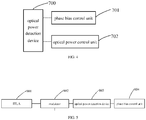
- FIG. 4 is a schematic structural diagram of an optical power detection apparatus according to an embodiment of the present disclosure.
- the optical power detection apparatus includes the optical power detection device 700 according to the embodiments of the present disclosure, and at least one of a phase bias control unit 701 and an optical power control unit 702.
- the phase bias control unit 701 and the optical power control unit 702 are respectively connected to the optical power detection device 700, and respectively receive a voltage signal output by the optical power detection device 700.
- a phase bias control unit 701 may be connected to a modulator to adjust a phase bias working point of the modulator.
- the optical power control unit 702 may be connected with a variable optical attenuator, and the output optical signal power is adjusted by controlling an attenuation value of the variable optical attenuator.
- the optical power detection device may be applied to a PM-QPSK transmitter, an erbium-doped fiber amplifier, a PM-16QAM transmitter and the like.
- FIG. 5 is a schematic structural diagram of a PM-QPSK transmitter including an optical power detection device according to an embodiment of the present disclosure.
- the transmitter using a Mach-Zehnder type modulator is a transmitter based on a PM-QPSK modulation device.
- a bias voltage of a modulator 802 is controlled by a pilot signal plus a DC value.
- the optical input to the modulator 802 uses a tunable laser (ITLA) 801 as a light source, and optical signals of continuous wavelengths emitted by the ITLA 801 are modulated by the modulator 802 to form optical output signals in an optical PM-QPSK modulation format.
- the data input to modulator 802 are 4-way signals output from a PM-QPSK signal source (not shown).
- the modulated optical signal output by the modulator 802 is input to an optical power detection device 803.
- the optical power detection device 803 may be an optical power detection device according to the embodiments of the present disclosure.
- the optical power detection device 803 splits the modulated optical signal into two parts, i.e., a first optical signal and a second optical signal.
- the second optical signal is coupled into an output port of the optical power detection device 803, i.e., a 100G network-side optical output port, as a main output signal.
- the first optical signal is coupled into the photocell 302, and the photocell 302 and the electrical amplification module 303 are disposed in the micro-shield 304 (see FIG.
- the amplitude of the voltage signal is in a proportional relationship with the total input optical signal power of the optical power detection device 803, and may reflect the magnitude of the total input optical power, so that the output optical signal power may be adjusted by controlling an attenuation value of the variable optical attenuator.
- the output of the electrical amplification module 303 in the optical power detection device 803 is transmitted to the phase bias control unit 804 to adjust a phase bias working point of the modulator 802.
- FIG. 6 is a schematic structural diagram of an erbium-doped fiber amplifier including an optical power detection device according to an embodiment of the present disclosure.
- the erbium-doped fiber amplifier includes: optical isolators 901, 905, 911 and 915; 980nm/1550nm wavelength division multiplexers (WDMs) 902, 912; 980nm pump lasers 903, 913; erbium-doped fibers 904 and 914, variable optical attenuators 906 and 916, an optical power detection device 908, an optical power control unit 907, and a Micro Control Unit (MCU) 909.
- the optical isolator 901, the wavelength division multiplexer 902, the erbium-doped fiber 904, the optical isolator 905, the variable optical attenuator 906 and the optical power detection device 908 are connected in sequence.
- the pump laser 903 is connected to the wavelength division multiplexer 902 to deliver energy to the erbium-doped fiber 904.
- the optical power control unit 907 is connected to an output end of the optical power detection device 908 and the MCU 909, respectively.
- the optical isolator 911, the wavelength division multiplexer 912, the erbium-doped fiber 914, the optical isolator 915, the variable optical attenuator 916 and the optical power detection device 908 are connected in sequence.
- the pump laser 913 is connected to the wavelength division multiplexer 912 to deliver energy to the erbium-doped fiber 914.
- the optical power control unit 917 is connected to an output end of the optical power detection device 908 and the MCU 909, respectively.
- a 1550nm optical signal is added from the input end, and energy from the 980nm pump laser is received in the erbium-doped fiber so that stimulated radiation is produced and a 1550nm optical signal with an enhanced power is output.
- Part of the optical signals split out by the optical power detection device 908 is used for detecting strength of the optical signals, and the rest optical signals are coupled into to the output port for transmission of the optical signals.
- the optical signal detected by the optical power detection device 908 is converted into an electrical signal, and then input to the optical power control units 907 and 917 as a negative feedback signal to control the variable optical attenuators 906 and 916 to output satisfactory optical signal strength.
- the optical power detection device 908 may be an optical power detection device according to the embodiments of the present disclosure.
- FIG. 7 is a schematic structural diagram of a PM-16QAM transmitter including an optical power detection device according to an embodiment of the present disclosure.
- an optical input to a modulator 113 uses a tunable laser, ITLA 111, as a light source.
- Optical signals of continuous wavelengths emitted by the ITLA 111 are modulated by the modulator 113 to form optical output signals in an optical 16QAM modulation format.
- the data input to the modulator 113 are signals amplified by a driver 112 from signals output of a two-channel 4-way signal source (not shown).
- the modulated optical signal output from the modulator 113 enters an optical power detection device 115 through a variable optical attenuator 114.
- the optical power detection device 115 splits the modulated optical signal into two parts, one is coupled into an output port of the optical power detection device 115, i.e., a 200G network-side optical output port, as a main output signal; and the other is coupled into the photocell 302, and the photocell 320 and the electrical amplification module 303 are disposed in the micro-shield 304 (see FIG. 1 ) to convert the input optical signal into a photocurrent, and then into a voltage signal for amplification.
- the amplitude of the voltage signal is in a proportional relationship with the total input optical signal power of the optical power detection device 115, and may reflect the magnitude of the total input optical power.
- the voltage signal is output to the optical power control unit 116 so that the output optical signal power may be adjusted by controlling an attenuation value of the variable optical attenuator 114. Further, the output of the electrical amplification module 303 in the optical power detection device 115 is transmitted to the phase bias control unit 117 to adjust a phase bias working point of the modulator 113.
- the present disclosure provides an optical power detection device in which the photocell and the electrical amplification module are encapsulated in the micro-shield to protect signals of the photocell and the electrical amplification module from external interference, thereby effectively saving material cost of the external shield as well as labor cost of welding and installation.
- the optical splitter, the photocell and the electrical amplification module are integrated, thereby improving the sensitivity and integration level while reducing the number of devices, and thus facilitating layout and wiring.
Landscapes
- Physics & Mathematics (AREA)
- General Physics & Mathematics (AREA)
- Spectroscopy & Molecular Physics (AREA)
- Engineering & Computer Science (AREA)
- Automation & Control Theory (AREA)
- Optical Modulation, Optical Deflection, Nonlinear Optics, Optical Demodulation, Optical Logic Elements (AREA)
- Optical Communication System (AREA)
- Geophysics And Detection Of Objects (AREA)
- Lasers (AREA)
- Amplifiers (AREA)
Abstract
Description
- The present disclosure relates to, but is not limited to, the field of optical fiber devices.
- With the continuous development of laser technology, laser devices are more and more widely applied to general technologies of various fields of modern society, and play important roles in communication, medical treatment, machining, radar, material processing and the like. Optical power detector is one of the key technologies in the laser device, which plays a role in photoelectric conversion of output optical signals in the device, and is an important part of a laser control loop, and optical signal detection is an essential and important link of the whole laser device system.
- Current optical power detectors used in the market include two independent functional units, i.e., a light splitting unit and a photodetection unit. The light splitting unit splits the emitted optical signal into two beams, one being output for external application, and the other being provided to the photodetection unit. The photodetection unit provides the detected optical signal to a light source control device which uses the optical signal detected by the photodetection unit in a negative feedback loop, so as to control the light source to output a stable and satisfactory laser source.
- In applications, the main optical power of the light source device is assigned to an optical output port of the device, and only a small proportion of the optical power is input to the photodetector, resulting in a very weak electric signal output by the photodetector. Thus, an external amplifier is required to amplify the weak electrical signal. However, the external amplifier unit is easily interfered by other strong electromagnetic signals, and if the interference signals are crossed into the control loop of the light emitting unit, normal work of the control device of the light emitting unit will be affected so that the control device of the light emitting unit cannot work stably at a set locking point, resulting in unlocking of the working point. The unlocking of the working point may cause instability of the overall light emitting device, and it is externally shown as failure of the light emitting device.
- In order to reduce the influence of interference, a metal shield for shielding electromagnetic interference needs to be additionally arranged. This kind of external shield needs to be installed manually, and is low in production efficiency, high in cost and unstable in working efficiency.
- According to an aspect of the disclosure, there is provided an optical power detection device, including: an optical splitter configured to split an input optical signal into a first optical signal and a second optical signal at a preset fixed proportion; a photocell connected to an output end of the optical splitter, the photocell being configured to receive the first optical signal output by the optical splitter and convert the first optical signal into a current signal; an electrical amplification module connected to an output end of the photocell, the electrical amplification module being configured to receive the current signal output by the photocell, convert the current signal into a voltage signal, and perform gain processing on and then output the voltage signal; and a micro-shield configured to encapsulate the photocell and the electrical amplification module.
- According to another aspect of the present disclosure, there is provided an optical power detection apparatus, including the optical power detection device of the present disclosure, and at least one of a phase bias control unit and an optical power control unit, wherein the phase bias control unit and the optical power control unit are respectively connected to the optical power detection device and respectively receive a voltage signal output by the optical power detection device.
- Accompanying drawings are provided for further understanding of the embodiments of the disclosure and constitute a part of the specification. Hereinafter, these drawings are intended to explain the disclosure together with the following embodiments, but should not be considered as a limitation to the disclosure. In the drawings:
-
FIG. 1 is a schematic structural diagram of an optical power detection device according to an embodiment of the present disclosure; -
FIG. 2 is a current-voltage characteristic curve of a photocell according to an embodiment of the disclosure; -
FIG. 3 is a schematic structural diagram of an electrical amplification module according to an embodiment of the disclosure; -
FIG. 4 is a schematic structural diagram of an optical power detection apparatus according to an embodiment of the present disclosure; -
FIG. 5 is a schematic structural diagram of a PM-QPSK transmitter including an optical power detection device according to an embodiment of the present disclosure; -
FIG. 6 is a schematic structural diagram of an erbium-doped fiber amplifier including an optical power detection device according to an embodiment of the present disclosure; and -
FIG. 7 is a schematic structural diagram of a PM-16QAM transmitter including an optical power detection device according to an embodiment of the present disclosure. - Implementations, functions, features and advantages of the present disclosure will be further explained below with reference to the embodiments and the accompanying drawings.
- For clarity and better understanding of the technical problems, technical solutions and beneficial effects of the present disclosure, the present disclosure will be further described in detail below in conjunction with the accompanying drawings and embodiments. It will be appreciated that the specific embodiments described herein are merely for illustration of the disclosure and are not intended to limit the disclosure.
- In the following description, elements described using terms, such as "module", "component" or "unit", are only used for facilitating description of the present disclosure, and have no specific meaning in themselves. Thus, "module", "component" or "unit" may be used interchangeably.
-
FIG. 1 is a schematic structural diagram of an optical power detection device according to an embodiment of the present disclosure. - As shown in
FIG. 1 , the optical power detection device according to an embodiment of the present disclosure includes anoptical splitter 301, aphotocell 302, anelectrical amplification module 303, and a micro-shield 304. Thephotocell 302 and theelectrical amplification module 303 may be integrated. - The
optical splitter 301 may split an input optical signal into a first optical signal and a second optical signal at a preset fixed proportion; and may adjust the proportion as needed. The proportion is not changeable any more after being determined, and it may be considered that the output optical power and the total input optical signal power are linearly proportional. The first optical signal may be used as an input signal of an optical detection branch, and the second optical signal may be used for output. - The
photocell 302 is connected to an output end of theoptical splitter 301 for outputting the first optical signal. Thephotocell 302 may receive the first optical signal output by theoptical splitter 301, and convert the first optical signal into a current signal. Thephotocell 302 may be a photodiode device for converting light energy into electric energy. For example, a PN junction photodiode may utilize the photosensitive property of the PN junction to convert the received light change into a current change. - The micro-shield 304 may encapsulate the
photocell 302 and theelectrical amplification module 303. Since the current output by thephotocell 302 is very weak, theelectrical amplification module 303 works in a weak small-signal state in which the current-voltage conversion process is easily interfered by external high-frequency signals. In this embodiment, thephotocell 302 and theelectrical amplification module 303 are encapsulated in the micro-shield 304 as a whole, so as to prevent external interference from affecting output of the voltage signal. The micro-shield 304 may shield interference of external electromagnetic signals. -
FIG. 2 is a current-voltage characteristic curve of a photocell according to an embodiment of the disclosure. - Referring to
FIG. 2 , in the absence of illumination, the photocell, like a common diode, has unidirectional conductivity, and when a forward voltage is applied externally, the current and the terminal voltage have an exponential relationship; when a reverse voltage is applied externally, the reverse current is called dark current and is generally less than 5 nA. In the presence of illumination, the characteristic curve moves downward. The characteristic curve is a set of parallel lines of the horizontal axis over a certain range of reverse voltages. The current generated by the photocell under illumination at the reverse voltage is called photocurrent, which is controlled by the incident light intensity. When the light intensity is constant, an optical detector may be equivalent to a constant current source. The greater the light intensity, the greater the photocurrent, and the photocurrent has a linear relationship with the light intensity when the photocurrent is greater than tens of microamperes. - Since the photoelectric conversion efficiency of the photodiode device directly affects the product performance, this index is generally required to be greater than 0.7 a/w. In addition, in order to reduce background noise interference, the dark current index is not greater than 5 nA. To expand the dynamic range of the input optical signal, the photocell is reversely biased.
- Returning to
FIG. 1 , theelectrical amplification module 303 is connected to an output end of thephotocell 302 for outputting current signals, receives the current signal output by thephotocell 302, converts the current signal into a voltage signal, and performs gain processing on and then outputs the voltage signal. - The micro-shield 304 may have, for example, a disc or cylindrical shape, but the embodiment of the present disclosure is not limited thereto. In a specific implementation, the micro-shield 304 may be provided with an optical communication via and an electrical communication via. The optical communication via is used for installation of a convex lens or passing of an optical fiber, thereby transmitting the first optical signal to the
photocell 302. The optical fiber may include a tapered optical fiber. The electrical communication via is used for passing of a power supply wire or a pin, so as to transmit the gain-processed voltage signal. -
FIG. 3 is a schematic structural diagram of an electrical amplification module according to an embodiment of the disclosure. - As shown in
FIG. 3 , theelectrical amplification module 303 according to an embodiment of the disclosure may include apre-amplifier 502 connected to an anode of thephotocell 302 via a PDA pin, and a post-amplifier 504 connected to thepre-amplifier 502. - The
pre-amplifier 502 converts the current signal output by thephotocell 302 into a voltage signal through afeedback resistor 503. Thepre-amplifier 502 may also control the gain of the voltage signal by changing the resistance of thefeedback resistor 503. - In an embodiment of the present disclosure, a power supply may supply power to the
pre-amplifier 502 via a VCC pin and avoltage regulator 501, so as to reduce power supply noise interference. The power supply may also be connected to a cathode of thephotocell 302 via avoltage regulator 501 and a PDC pin. - The post-amplifier 504 performs gain processing on the voltage signal converted by the
pre-amplifier 502. To increase the dynamic range of the input signal and maintain a fixed signal output range, the gain of the post-amplifier 504 is processed by an Automatic Gain Control (AGC) unit. - In an embodiment of the present disclosure, the
electrical amplification module 303 may further include a low frequencyfeedback loop unit 505 and a Received Signal Strength Indication (RSSI)unit 506 connected to the low frequencyfeedback loop unit 505. The low frequencyfeedback loop unit 505 is connected to the post-amplifier 504 to eliminate a DC signal component in an input signal of theelectrical amplification module 303. The signal output by the post-amplifier 504 is output after the DC signal component is removed by the low frequencyfeedback loop unit 505. The low frequencyfeedback loop unit 505 may include a DC restorer, and two resistors connected to the DC restorer. -
FIG. 4 is a schematic structural diagram of an optical power detection apparatus according to an embodiment of the present disclosure. - As shown in
FIG. 4 , the optical power detection apparatus according to an embodiment of the present disclosure includes the opticalpower detection device 700 according to the embodiments of the present disclosure, and at least one of a phasebias control unit 701 and an opticalpower control unit 702. The phasebias control unit 701 and the opticalpower control unit 702 are respectively connected to the opticalpower detection device 700, and respectively receive a voltage signal output by the opticalpower detection device 700. - Typically, a phase
bias control unit 701 may be connected to a modulator to adjust a phase bias working point of the modulator. The opticalpower control unit 702 may be connected with a variable optical attenuator, and the output optical signal power is adjusted by controlling an attenuation value of the variable optical attenuator. - The optical power detection device according to the embodiment of the disclosure may be applied to a PM-QPSK transmitter, an erbium-doped fiber amplifier, a PM-16QAM transmitter and the like.
-
FIG. 5 is a schematic structural diagram of a PM-QPSK transmitter including an optical power detection device according to an embodiment of the present disclosure. - As shown in
FIG. 5 , in an optical transmitter for implementing a 100 Gbit/s high-speed optical transmission device, the transmitter using a Mach-Zehnder type modulator is a transmitter based on a PM-QPSK modulation device. A bias voltage of amodulator 802 is controlled by a pilot signal plus a DC value. - The optical input to the
modulator 802 uses a tunable laser (ITLA) 801 as a light source, and optical signals of continuous wavelengths emitted by theITLA 801 are modulated by themodulator 802 to form optical output signals in an optical PM-QPSK modulation format. The data input tomodulator 802 are 4-way signals output from a PM-QPSK signal source (not shown). - The modulated optical signal output by the
modulator 802 is input to an opticalpower detection device 803. The opticalpower detection device 803 may be an optical power detection device according to the embodiments of the present disclosure. The opticalpower detection device 803 splits the modulated optical signal into two parts, i.e., a first optical signal and a second optical signal. The second optical signal is coupled into an output port of the opticalpower detection device 803, i.e., a 100G network-side optical output port, as a main output signal. The first optical signal is coupled into thephotocell 302, and thephotocell 302 and theelectrical amplification module 303 are disposed in the micro-shield 304 (seeFIG. 1 ) to convert the input optical signal into a photocurrent, and then into a voltage signal for amplification. The amplitude of the voltage signal is in a proportional relationship with the total input optical signal power of the opticalpower detection device 803, and may reflect the magnitude of the total input optical power, so that the output optical signal power may be adjusted by controlling an attenuation value of the variable optical attenuator. The output of theelectrical amplification module 303 in the opticalpower detection device 803 is transmitted to the phasebias control unit 804 to adjust a phase bias working point of themodulator 802. -
FIG. 6 is a schematic structural diagram of an erbium-doped fiber amplifier including an optical power detection device according to an embodiment of the present disclosure. - As shown in
FIG. 6 , the erbium-doped fiber amplifier includes:optical isolators 980nm pump lasers fibers optical attenuators power detection device 908, an opticalpower control unit 907, and a Micro Control Unit (MCU) 909. Theoptical isolator 901, thewavelength division multiplexer 902, the erbium-dopedfiber 904, theoptical isolator 905, the variableoptical attenuator 906 and the opticalpower detection device 908 are connected in sequence. Thepump laser 903 is connected to thewavelength division multiplexer 902 to deliver energy to the erbium-dopedfiber 904. The opticalpower control unit 907 is connected to an output end of the opticalpower detection device 908 and theMCU 909, respectively. Theoptical isolator 911, thewavelength division multiplexer 912, the erbium-dopedfiber 914, theoptical isolator 915, the variableoptical attenuator 916 and the opticalpower detection device 908 are connected in sequence. Thepump laser 913 is connected to thewavelength division multiplexer 912 to deliver energy to the erbium-dopedfiber 914. The opticalpower control unit 917 is connected to an output end of the opticalpower detection device 908 and theMCU 909, respectively. In actual use, for two groups of input optical signals, one reaches the opticalpower detection device 908 via theoptical isolator 901, thewavelength division multiplexer 902, the erbium-dopedfiber 904, theoptical isolator 905 and the variableoptical attenuator 906, and the other reaches the opticalpower detection device 908 via theoptical isolator 911, thewavelength division multiplexer 912, the erbium-dopedfiber 914, theoptical isolator 915 and the variableoptical attenuator 916. - In this embodiment, a 1550nm optical signal is added from the input end, and energy from the 980nm pump laser is received in the erbium-doped fiber so that stimulated radiation is produced and a 1550nm optical signal with an enhanced power is output.
- Part of the optical signals split out by the optical
power detection device 908 is used for detecting strength of the optical signals, and the rest optical signals are coupled into to the output port for transmission of the optical signals. The optical signal detected by the opticalpower detection device 908 is converted into an electrical signal, and then input to the opticalpower control units optical attenuators - The optical
power detection device 908 may be an optical power detection device according to the embodiments of the present disclosure. -
FIG. 7 is a schematic structural diagram of a PM-16QAM transmitter including an optical power detection device according to an embodiment of the present disclosure. - As shown in
Fig. 7 , in a 200G PM-16QAM transmitter, an optical input to amodulator 113 uses a tunable laser, ITLA 111, as a light source. Optical signals of continuous wavelengths emitted by the ITLA 111 are modulated by themodulator 113 to form optical output signals in an optical 16QAM modulation format. The data input to themodulator 113 are signals amplified by adriver 112 from signals output of a two-channel 4-way signal source (not shown). - The modulated optical signal output from the
modulator 113 enters an opticalpower detection device 115 through a variableoptical attenuator 114. The opticalpower detection device 115 splits the modulated optical signal into two parts, one is coupled into an output port of the opticalpower detection device 115, i.e., a 200G network-side optical output port, as a main output signal; and the other is coupled into thephotocell 302, and the photocell 320 and theelectrical amplification module 303 are disposed in the micro-shield 304 (seeFIG. 1 ) to convert the input optical signal into a photocurrent, and then into a voltage signal for amplification. The amplitude of the voltage signal is in a proportional relationship with the total input optical signal power of the opticalpower detection device 115, and may reflect the magnitude of the total input optical power. The voltage signal is output to the opticalpower control unit 116 so that the output optical signal power may be adjusted by controlling an attenuation value of the variableoptical attenuator 114. Further, the output of theelectrical amplification module 303 in the opticalpower detection device 115 is transmitted to the phasebias control unit 117 to adjust a phase bias working point of themodulator 113. - The present disclosure provides an optical power detection device in which the photocell and the electrical amplification module are encapsulated in the micro-shield to protect signals of the photocell and the electrical amplification module from external interference, thereby effectively saving material cost of the external shield as well as labor cost of welding and installation. In the present disclosure, the optical splitter, the photocell and the electrical amplification module are integrated, thereby improving the sensitivity and integration level while reducing the number of devices, and thus facilitating layout and wiring.
- The embodiments of the present disclosure have been described above with reference to the accompanying drawings, but the scope of the present disclosure is not limited thereby. Those skilled in the art can implement the present disclosure in various modifications without departing from the scope and spirit of the present disclosure, e.g., features from one embodiment can be used in another embodiment to yield yet a further embodiment. Any modification, equivalent replacement or improvement made within the technical concept of the present disclosure shall fall in the scope of the claims of the present disclosure.
Claims (8)
- An optical power detection device, comprising:an optical splitter configured to split an input optical signal into a first optical signal and a second optical signal at a preset fixed proportion;a photocell connected to an output end of the optical splitter, the photocell being configured to receive the first optical signal output by the optical splitter and convert the first optical signal into a current signal;an electrical amplification module connected to an output end of the photocell, the electrical amplification module being configured to receive the current signal output by the photocell, convert the current signal into a voltage signal, and perform gain processing on and then output the voltage signal; anda micro-shield configured to encapsulate the photocell and the electrical amplification module.
- The optical power detection device of claim 1, wherein the photocell is reversely biased.
- The optical power detection device of claim 1, wherein the electrical amplification module comprises:a pre-amplifier connected to an anode of the photocell, the pre-amplifier being configured to convert a current signal into a voltage signal through a feedback resistor; anda post-amplifier connected to the pre-amplifier, the post-amplifier being configured to perform gain processing on the voltage signal converted by the pre-amplifier.
- The optical power detection device of claim 3, wherein the electrical amplification module further comprises:
a low frequency feedback loop unit connected to the post-amplifier, the low frequency feedback loop unit being configured to eliminate a DC signal component in an input signal of the electrical amplification module. - The optical power detection device of claim 4, wherein the electrical amplification module further comprises:
a received signal strength indication unit connected to the low frequency feedback loop unit. - The optical power detection device of claim 3, wherein the electrical amplification module further comprises:
a power supply connected to the pre-amplifier and a cathode of the photocell. - The optical power detection device of claim 1, wherein the micro-shield is provided with an optical communication via and an electrical communication via.
- An optical power detection apparatus, comprising the optical power detection device according to any one of claims 1-7, the optical power detection apparatus further comprising at least one of a phase bias control unit and an optical power control unit, wherein
the phase bias control unit and the optical power control unit are respectively connected to the optical power detection device and respectively receive a voltage signal output by the optical power detection device.
Applications Claiming Priority (2)
| Application Number | Priority Date | Filing Date | Title |
|---|---|---|---|
| CN201721144064.4U CN207570667U (en) | 2017-09-07 | 2017-09-07 | The detection device and equipment of luminous power |
| PCT/CN2018/104613 WO2019047923A1 (en) | 2017-09-07 | 2018-09-07 | Optical power detection device and device |
Publications (3)
| Publication Number | Publication Date |
|---|---|
| EP3680633A1 true EP3680633A1 (en) | 2020-07-15 |
| EP3680633A4 EP3680633A4 (en) | 2021-06-30 |
| EP3680633B1 EP3680633B1 (en) | 2025-04-30 |
Family
ID=62698241
Family Applications (1)
| Application Number | Title | Priority Date | Filing Date |
|---|---|---|---|
| EP18853370.7A Active EP3680633B1 (en) | 2017-09-07 | 2018-09-07 | Optical power detection device and apparatus |
Country Status (4)
| Country | Link |
|---|---|
| EP (1) | EP3680633B1 (en) |
| KR (1) | KR102443309B1 (en) |
| CN (1) | CN207570667U (en) |
| WO (1) | WO2019047923A1 (en) |
Families Citing this family (4)
| Publication number | Priority date | Publication date | Assignee | Title |
|---|---|---|---|---|
| CN207570667U (en) * | 2017-09-07 | 2018-07-03 | 中兴通讯股份有限公司 | The detection device and equipment of luminous power |
| CN110440914B (en) * | 2019-07-10 | 2021-07-23 | 武汉精测电子集团股份有限公司 | Noise reduction system for photoelectric detection and AOI detection equipment |
| CN112317558B (en) * | 2020-09-04 | 2023-01-17 | 中国第一汽车股份有限公司 | Rapid electrical detection system and method for sheet number of stamping automatic line |
| CN116429250B (en) * | 2023-06-14 | 2023-10-13 | 深圳深浦电气有限公司 | Photoelectric detection circuit, photoelectric detection method, and photoelectric sensor |
Family Cites Families (11)
| Publication number | Priority date | Publication date | Assignee | Title |
|---|---|---|---|---|
| US4611600A (en) * | 1983-11-21 | 1986-09-16 | Cordis Corporation | Optical fiber pressure transducer |
| JPH0634473A (en) * | 1992-07-21 | 1994-02-08 | Mitsubishi Heavy Ind Ltd | Gas pressure measuring device |
| JP3461645B2 (en) * | 1995-12-12 | 2003-10-27 | 富士通株式会社 | Light intensity measurement device |
| JP3425310B2 (en) * | 1996-11-25 | 2003-07-14 | シャープ株式会社 | Light emitting / receiving device |
| CN1225868C (en) * | 2002-07-18 | 2005-11-02 | 华为技术有限公司 | Flow rate protecting method and device for light interface in data communication equipment |
| CN101170360B (en) * | 2006-10-25 | 2011-05-11 | 中兴通讯股份有限公司 | A signal optical power detection device and detection method |
| CN201368769Y (en) * | 2008-12-31 | 2009-12-23 | 北京工业大学 | Laser light power real-time on-line checking device of semiconductor laser |
| CN202066590U (en) * | 2011-02-22 | 2011-12-07 | 闫妍 | Laser power detecting apparatus |
| CN106949961B (en) * | 2017-03-22 | 2018-07-31 | 精微视达医疗科技(武汉)有限公司 | Luminous power monitoring in real time and feedback method and device |
| CN107104724A (en) * | 2017-04-21 | 2017-08-29 | 广西师范大学 | A kind of light line protective device |
| CN207570667U (en) * | 2017-09-07 | 2018-07-03 | 中兴通讯股份有限公司 | The detection device and equipment of luminous power |
-
2017
- 2017-09-07 CN CN201721144064.4U patent/CN207570667U/en active Active
-
2018
- 2018-09-07 WO PCT/CN2018/104613 patent/WO2019047923A1/en not_active Ceased
- 2018-09-07 KR KR1020207006625A patent/KR102443309B1/en active Active
- 2018-09-07 EP EP18853370.7A patent/EP3680633B1/en active Active
Also Published As
| Publication number | Publication date |
|---|---|
| WO2019047923A1 (en) | 2019-03-14 |
| CN207570667U (en) | 2018-07-03 |
| EP3680633B1 (en) | 2025-04-30 |
| KR20200036012A (en) | 2020-04-06 |
| EP3680633A4 (en) | 2021-06-30 |
| KR102443309B1 (en) | 2022-09-14 |
Similar Documents
| Publication | Publication Date | Title |
|---|---|---|
| EP3680633B1 (en) | Optical power detection device and apparatus | |
| US8774635B2 (en) | Fiber-optic automatic gain control systems and methods | |
| US11770192B2 (en) | Wavelength locking optical module, device, and wavelength locking method | |
| US20070258722A1 (en) | Optical receiver | |
| CA2062216C (en) | Optical-to-electric transducer with extended dynamic range | |
| US7297922B2 (en) | Optical receiver protection circuit | |
| CN102820931A (en) | Optical module of dual-mode optical network unit | |
| CN109743113B (en) | Optical module and optical line terminal | |
| KR20220036646A (en) | Method and Apparatus for Tracking in Optical Wireless Communication with beam forming function | |
| CN107026694A (en) | A kind of output signal control method of feedback control circuit and Electro-Optical Sensor Set | |
| JP6927785B2 (en) | Control method of optical amplifier and optical amplifier | |
| JP5750920B2 (en) | Optical receiver module | |
| JP6182897B2 (en) | Optical receiver and optical receiving method | |
| CN105514784A (en) | Power-controllable single-channel erbium-doped fiber amplifier | |
| US20160182157A1 (en) | Optical receiver and optical reception method | |
| CN201577092U (en) | Passive optical network transmitting and receiving device | |
| CN105807534A (en) | Working mode selectable intelligent semiconductor fiber optic amplifier | |
| JP5938007B2 (en) | Optical receiving apparatus and optical receiving method | |
| JP2024060711A (en) | Light-receiving circuit | |
| JP2013197200A (en) | Photoreceiver control method and communication control method | |
| KR20110067777A (en) | Optical transmission and reception control device | |
| CN120357970B (en) | Optical receiving device, optical component and signal amplifying device | |
| JPH07202311A (en) | Optical semiconductor laser device wavelength stabilization method | |
| CN220137448U (en) | Optical structure and optical module | |
| CZ36461U1 (en) | Optical detection module |
Legal Events
| Date | Code | Title | Description |
|---|---|---|---|
| STAA | Information on the status of an ep patent application or granted ep patent |
Free format text: STATUS: THE INTERNATIONAL PUBLICATION HAS BEEN MADE |
|
| PUAI | Public reference made under article 153(3) epc to a published international application that has entered the european phase |
Free format text: ORIGINAL CODE: 0009012 |
|
| STAA | Information on the status of an ep patent application or granted ep patent |
Free format text: STATUS: REQUEST FOR EXAMINATION WAS MADE |
|
| 17P | Request for examination filed |
Effective date: 20200227 |
|
| AK | Designated contracting states |
Kind code of ref document: A1 Designated state(s): AL AT BE BG CH CY CZ DE DK EE ES FI FR GB GR HR HU IE IS IT LI LT LU LV MC MK MT NL NO PL PT RO RS SE SI SK SM TR |
|
| AX | Request for extension of the european patent |
Extension state: BA ME |
|
| DAV | Request for validation of the european patent (deleted) | ||
| DAX | Request for extension of the european patent (deleted) | ||
| A4 | Supplementary search report drawn up and despatched |
Effective date: 20210601 |
|
| RIC1 | Information provided on ipc code assigned before grant |
Ipc: G01J 1/44 20060101AFI20210526BHEP Ipc: G01J 1/04 20060101ALI20210526BHEP Ipc: G05D 25/02 20060101ALI20210526BHEP |
|
| STAA | Information on the status of an ep patent application or granted ep patent |
Free format text: STATUS: EXAMINATION IS IN PROGRESS |
|
| 17Q | First examination report despatched |
Effective date: 20230405 |
|
| GRAP | Despatch of communication of intention to grant a patent |
Free format text: ORIGINAL CODE: EPIDOSNIGR1 |
|
| STAA | Information on the status of an ep patent application or granted ep patent |
Free format text: STATUS: GRANT OF PATENT IS INTENDED |
|
| GRAS | Grant fee paid |
Free format text: ORIGINAL CODE: EPIDOSNIGR3 |
|
| GRAA | (expected) grant |
Free format text: ORIGINAL CODE: 0009210 |
|
| STAA | Information on the status of an ep patent application or granted ep patent |
Free format text: STATUS: THE PATENT HAS BEEN GRANTED |
|
| INTG | Intention to grant announced |
Effective date: 20250228 |
|
| AK | Designated contracting states |
Kind code of ref document: B1 Designated state(s): AL AT BE BG CH CY CZ DE DK EE ES FI FR GB GR HR HU IE IS IT LI LT LU LV MC MK MT NL NO PL PT RO RS SE SI SK SM TR |
|
| REG | Reference to a national code |
Ref country code: CH Ref legal event code: EP Ref country code: GB Ref legal event code: FG4D |
|
| REG | Reference to a national code |
Ref country code: IE Ref legal event code: FG4D |
|
| REG | Reference to a national code |
Ref country code: DE Ref legal event code: R096 Ref document number: 602018081600 Country of ref document: DE |
|
| REG | Reference to a national code |
Ref country code: NL Ref legal event code: MP Effective date: 20250430 |
|
| REG | Reference to a national code |
Ref country code: AT Ref legal event code: MK05 Ref document number: 1790402 Country of ref document: AT Kind code of ref document: T Effective date: 20250430 |
|
| PG25 | Lapsed in a contracting state [announced via postgrant information from national office to epo] |
Ref country code: ES Free format text: LAPSE BECAUSE OF FAILURE TO SUBMIT A TRANSLATION OF THE DESCRIPTION OR TO PAY THE FEE WITHIN THE PRESCRIBED TIME-LIMIT Effective date: 20250430 Ref country code: FI Free format text: LAPSE BECAUSE OF FAILURE TO SUBMIT A TRANSLATION OF THE DESCRIPTION OR TO PAY THE FEE WITHIN THE PRESCRIBED TIME-LIMIT Effective date: 20250430 Ref country code: PT Free format text: LAPSE BECAUSE OF FAILURE TO SUBMIT A TRANSLATION OF THE DESCRIPTION OR TO PAY THE FEE WITHIN THE PRESCRIBED TIME-LIMIT Effective date: 20250901 |
|
| PGFP | Annual fee paid to national office [announced via postgrant information from national office to epo] |
Ref country code: DE Payment date: 20250702 Year of fee payment: 8 |
|
| REG | Reference to a national code |
Ref country code: LT Ref legal event code: MG9D |
|
| PG25 | Lapsed in a contracting state [announced via postgrant information from national office to epo] |
Ref country code: GR Free format text: LAPSE BECAUSE OF FAILURE TO SUBMIT A TRANSLATION OF THE DESCRIPTION OR TO PAY THE FEE WITHIN THE PRESCRIBED TIME-LIMIT Effective date: 20250731 Ref country code: NO Free format text: LAPSE BECAUSE OF FAILURE TO SUBMIT A TRANSLATION OF THE DESCRIPTION OR TO PAY THE FEE WITHIN THE PRESCRIBED TIME-LIMIT Effective date: 20250730 |
|
| PG25 | Lapsed in a contracting state [announced via postgrant information from national office to epo] |
Ref country code: PL Free format text: LAPSE BECAUSE OF FAILURE TO SUBMIT A TRANSLATION OF THE DESCRIPTION OR TO PAY THE FEE WITHIN THE PRESCRIBED TIME-LIMIT Effective date: 20250430 Ref country code: NL Free format text: LAPSE BECAUSE OF FAILURE TO SUBMIT A TRANSLATION OF THE DESCRIPTION OR TO PAY THE FEE WITHIN THE PRESCRIBED TIME-LIMIT Effective date: 20250430 |
|
| PGFP | Annual fee paid to national office [announced via postgrant information from national office to epo] |
Ref country code: TR Payment date: 20250903 Year of fee payment: 8 |
|
| PG25 | Lapsed in a contracting state [announced via postgrant information from national office to epo] |
Ref country code: BG Free format text: LAPSE BECAUSE OF FAILURE TO SUBMIT A TRANSLATION OF THE DESCRIPTION OR TO PAY THE FEE WITHIN THE PRESCRIBED TIME-LIMIT Effective date: 20250430 |
|
| PG25 | Lapsed in a contracting state [announced via postgrant information from national office to epo] |
Ref country code: HR Free format text: LAPSE BECAUSE OF FAILURE TO SUBMIT A TRANSLATION OF THE DESCRIPTION OR TO PAY THE FEE WITHIN THE PRESCRIBED TIME-LIMIT Effective date: 20250430 |
|
| PG25 | Lapsed in a contracting state [announced via postgrant information from national office to epo] |
Ref country code: AT Free format text: LAPSE BECAUSE OF FAILURE TO SUBMIT A TRANSLATION OF THE DESCRIPTION OR TO PAY THE FEE WITHIN THE PRESCRIBED TIME-LIMIT Effective date: 20250430 |
|
| PG25 | Lapsed in a contracting state [announced via postgrant information from national office to epo] |
Ref country code: RS Free format text: LAPSE BECAUSE OF FAILURE TO SUBMIT A TRANSLATION OF THE DESCRIPTION OR TO PAY THE FEE WITHIN THE PRESCRIBED TIME-LIMIT Effective date: 20250731 |
|
| PG25 | Lapsed in a contracting state [announced via postgrant information from national office to epo] |
Ref country code: IS Free format text: LAPSE BECAUSE OF FAILURE TO SUBMIT A TRANSLATION OF THE DESCRIPTION OR TO PAY THE FEE WITHIN THE PRESCRIBED TIME-LIMIT Effective date: 20250830 |
|
| PG25 | Lapsed in a contracting state [announced via postgrant information from national office to epo] |
Ref country code: LV Free format text: LAPSE BECAUSE OF FAILURE TO SUBMIT A TRANSLATION OF THE DESCRIPTION OR TO PAY THE FEE WITHIN THE PRESCRIBED TIME-LIMIT Effective date: 20250430 |
|
| PG25 | Lapsed in a contracting state [announced via postgrant information from national office to epo] |
Ref country code: DK Free format text: LAPSE BECAUSE OF FAILURE TO SUBMIT A TRANSLATION OF THE DESCRIPTION OR TO PAY THE FEE WITHIN THE PRESCRIBED TIME-LIMIT Effective date: 20250430 Ref country code: SM Free format text: LAPSE BECAUSE OF FAILURE TO SUBMIT A TRANSLATION OF THE DESCRIPTION OR TO PAY THE FEE WITHIN THE PRESCRIBED TIME-LIMIT Effective date: 20250430 |
|
| PG25 | Lapsed in a contracting state [announced via postgrant information from national office to epo] |
Ref country code: CZ Free format text: LAPSE BECAUSE OF FAILURE TO SUBMIT A TRANSLATION OF THE DESCRIPTION OR TO PAY THE FEE WITHIN THE PRESCRIBED TIME-LIMIT Effective date: 20250430 |
|
| PG25 | Lapsed in a contracting state [announced via postgrant information from national office to epo] |
Ref country code: EE Free format text: LAPSE BECAUSE OF FAILURE TO SUBMIT A TRANSLATION OF THE DESCRIPTION OR TO PAY THE FEE WITHIN THE PRESCRIBED TIME-LIMIT Effective date: 20250430 |
|
| PG25 | Lapsed in a contracting state [announced via postgrant information from national office to epo] |
Ref country code: RO Free format text: LAPSE BECAUSE OF FAILURE TO SUBMIT A TRANSLATION OF THE DESCRIPTION OR TO PAY THE FEE WITHIN THE PRESCRIBED TIME-LIMIT Effective date: 20250430 Ref country code: SK Free format text: LAPSE BECAUSE OF FAILURE TO SUBMIT A TRANSLATION OF THE DESCRIPTION OR TO PAY THE FEE WITHIN THE PRESCRIBED TIME-LIMIT Effective date: 20250430 |
|
| PG25 | Lapsed in a contracting state [announced via postgrant information from national office to epo] |
Ref country code: IT Free format text: LAPSE BECAUSE OF FAILURE TO SUBMIT A TRANSLATION OF THE DESCRIPTION OR TO PAY THE FEE WITHIN THE PRESCRIBED TIME-LIMIT Effective date: 20250430 |
|
| REG | Reference to a national code |
Ref country code: DE Ref legal event code: R097 Ref document number: 602018081600 Country of ref document: DE |
|
| PLBE | No opposition filed within time limit |
Free format text: ORIGINAL CODE: 0009261 |
|
| STAA | Information on the status of an ep patent application or granted ep patent |
Free format text: STATUS: NO OPPOSITION FILED WITHIN TIME LIMIT |
|
| REG | Reference to a national code |
Ref country code: CH Ref legal event code: L10 Free format text: ST27 STATUS EVENT CODE: U-0-0-L10-L00 (AS PROVIDED BY THE NATIONAL OFFICE) Effective date: 20260311 |
|
| 26N | No opposition filed |
Effective date: 20260202 |
|
| REG | Reference to a national code |
Ref country code: CH Ref legal event code: H13 Free format text: ST27 STATUS EVENT CODE: U-0-0-H10-H13 (AS PROVIDED BY THE NATIONAL OFFICE) Effective date: 20260504 |
|
| PG25 | Lapsed in a contracting state [announced via postgrant information from national office to epo] |
Ref country code: LU Free format text: LAPSE BECAUSE OF NON-PAYMENT OF DUE FEES Effective date: 20250907 |
|
| GBPC | Gb: european patent ceased through non-payment of renewal fee |
Effective date: 20250907 |
|
| REG | Reference to a national code |
Ref country code: BE Ref legal event code: MM Effective date: 20250930 |
|
| PG25 | Lapsed in a contracting state [announced via postgrant information from national office to epo] |
Ref country code: LT Free format text: LAPSE BECAUSE OF FAILURE TO SUBMIT A TRANSLATION OF THE DESCRIPTION OR TO PAY THE FEE WITHIN THE PRESCRIBED TIME-LIMIT Effective date: 20250430 |
|
| PG25 | Lapsed in a contracting state [announced via postgrant information from national office to epo] |
Ref country code: MC Free format text: LAPSE BECAUSE OF FAILURE TO SUBMIT A TRANSLATION OF THE DESCRIPTION OR TO PAY THE FEE WITHIN THE PRESCRIBED TIME-LIMIT Effective date: 20250430 |
|
| PG25 | Lapsed in a contracting state [announced via postgrant information from national office to epo] |
Ref country code: GB Free format text: LAPSE BECAUSE OF NON-PAYMENT OF DUE FEES Effective date: 20250907 |
|
| PG25 | Lapsed in a contracting state [announced via postgrant information from national office to epo] |
Ref country code: BE Free format text: LAPSE BECAUSE OF NON-PAYMENT OF DUE FEES Effective date: 20250930 Ref country code: CH Free format text: LAPSE BECAUSE OF NON-PAYMENT OF DUE FEES Effective date: 20250930 Ref country code: IE Free format text: LAPSE BECAUSE OF NON-PAYMENT OF DUE FEES Effective date: 20250907 |
|
| PG25 | Lapsed in a contracting state [announced via postgrant information from national office to epo] |
Ref country code: FR Free format text: LAPSE BECAUSE OF NON-PAYMENT OF DUE FEES Effective date: 20250930 |
|
| PG25 | Lapsed in a contracting state [announced via postgrant information from national office to epo] |
Ref country code: SE Free format text: LAPSE BECAUSE OF FAILURE TO SUBMIT A TRANSLATION OF THE DESCRIPTION OR TO PAY THE FEE WITHIN THE PRESCRIBED TIME-LIMIT Effective date: 20250430 |