EP3679602B1 - Thermische strukturen zur ableitung von wärme und verfahren zur herstellung davon - Google Patents
Thermische strukturen zur ableitung von wärme und verfahren zur herstellung davon Download PDFInfo
- Publication number
- EP3679602B1 EP3679602B1 EP18759976.6A EP18759976A EP3679602B1 EP 3679602 B1 EP3679602 B1 EP 3679602B1 EP 18759976 A EP18759976 A EP 18759976A EP 3679602 B1 EP3679602 B1 EP 3679602B1
- Authority
- EP
- European Patent Office
- Prior art keywords
- metal
- copper
- base layer
- diamond
- layer
- Prior art date
- Legal status (The legal status is an assumption and is not a legal conclusion. Google has not performed a legal analysis and makes no representation as to the accuracy of the status listed.)
- Active
Links
Images





Classifications
-
- H—ELECTRICITY
- H10—SEMICONDUCTOR DEVICES; ELECTRIC SOLID-STATE DEVICES NOT OTHERWISE PROVIDED FOR
- H10W—GENERIC PACKAGES, INTERCONNECTIONS, CONNECTORS OR OTHER CONSTRUCTIONAL DETAILS OF DEVICES COVERED BY CLASS H10
- H10W40/00—Arrangements for thermal protection or thermal control
- H10W40/20—Arrangements for cooling
- H10W40/22—Arrangements for cooling characterised by their shape, e.g. having conical or cylindrical projections
- H10W40/226—Arrangements for cooling characterised by their shape, e.g. having conical or cylindrical projections characterised by projecting parts, e.g. fins to increase surface area
-
- H—ELECTRICITY
- H10—SEMICONDUCTOR DEVICES; ELECTRIC SOLID-STATE DEVICES NOT OTHERWISE PROVIDED FOR
- H10W—GENERIC PACKAGES, INTERCONNECTIONS, CONNECTORS OR OTHER CONSTRUCTIONAL DETAILS OF DEVICES COVERED BY CLASS H10
- H10W40/00—Arrangements for thermal protection or thermal control
- H10W40/20—Arrangements for cooling
- H10W40/25—Arrangements for cooling characterised by their materials
- H10W40/254—Diamond
-
- H—ELECTRICITY
- H10—SEMICONDUCTOR DEVICES; ELECTRIC SOLID-STATE DEVICES NOT OTHERWISE PROVIDED FOR
- H10W—GENERIC PACKAGES, INTERCONNECTIONS, CONNECTORS OR OTHER CONSTRUCTIONAL DETAILS OF DEVICES COVERED BY CLASS H10
- H10W40/00—Arrangements for thermal protection or thermal control
- H10W40/20—Arrangements for cooling
- H10W40/25—Arrangements for cooling characterised by their materials
- H10W40/257—Arrangements for cooling characterised by their materials having a heterogeneous or anisotropic structure, e.g. powder or fibres in a matrix, wire mesh or porous structures
-
- H—ELECTRICITY
- H10—SEMICONDUCTOR DEVICES; ELECTRIC SOLID-STATE DEVICES NOT OTHERWISE PROVIDED FOR
- H10W—GENERIC PACKAGES, INTERCONNECTIONS, CONNECTORS OR OTHER CONSTRUCTIONAL DETAILS OF DEVICES COVERED BY CLASS H10
- H10W40/00—Arrangements for thermal protection or thermal control
- H10W40/20—Arrangements for cooling
- H10W40/25—Arrangements for cooling characterised by their materials
- H10W40/258—Metallic materials
-
- H—ELECTRICITY
- H10—SEMICONDUCTOR DEVICES; ELECTRIC SOLID-STATE DEVICES NOT OTHERWISE PROVIDED FOR
- H10W—GENERIC PACKAGES, INTERCONNECTIONS, CONNECTORS OR OTHER CONSTRUCTIONAL DETAILS OF DEVICES COVERED BY CLASS H10
- H10W70/00—Package substrates; Interposers; Redistribution layers [RDL]
- H10W70/01—Manufacture or treatment
- H10W70/02—Manufacture or treatment of conductive package substrates serving as an interconnection, e.g. of metal plates
-
- C—CHEMISTRY; METALLURGY
- C23—COATING METALLIC MATERIAL; COATING MATERIAL WITH METALLIC MATERIAL; CHEMICAL SURFACE TREATMENT; DIFFUSION TREATMENT OF METALLIC MATERIAL; COATING BY VACUUM EVAPORATION, BY SPUTTERING, BY ION IMPLANTATION OR BY CHEMICAL VAPOUR DEPOSITION, IN GENERAL; INHIBITING CORROSION OF METALLIC MATERIAL OR INCRUSTATION IN GENERAL
- C23C—COATING METALLIC MATERIAL; COATING MATERIAL WITH METALLIC MATERIAL; SURFACE TREATMENT OF METALLIC MATERIAL BY DIFFUSION INTO THE SURFACE, BY CHEMICAL CONVERSION OR SUBSTITUTION; COATING BY VACUUM EVAPORATION, BY SPUTTERING, BY ION IMPLANTATION OR BY CHEMICAL VAPOUR DEPOSITION, IN GENERAL
- C23C24/00—Coating starting from inorganic powder
- C23C24/02—Coating starting from inorganic powder by application of pressure only
- C23C24/04—Impact or kinetic deposition of particles
-
- H—ELECTRICITY
- H10—SEMICONDUCTOR DEVICES; ELECTRIC SOLID-STATE DEVICES NOT OTHERWISE PROVIDED FOR
- H10W—GENERIC PACKAGES, INTERCONNECTIONS, CONNECTORS OR OTHER CONSTRUCTIONAL DETAILS OF DEVICES COVERED BY CLASS H10
- H10W40/00—Arrangements for thermal protection or thermal control
- H10W40/70—Fillings or auxiliary members in containers or in encapsulations for thermal protection or control
-
- H—ELECTRICITY
- H10—SEMICONDUCTOR DEVICES; ELECTRIC SOLID-STATE DEVICES NOT OTHERWISE PROVIDED FOR
- H10W—GENERIC PACKAGES, INTERCONNECTIONS, CONNECTORS OR OTHER CONSTRUCTIONAL DETAILS OF DEVICES COVERED BY CLASS H10
- H10W72/00—Interconnections or connectors in packages
- H10W72/851—Dispositions of multiple connectors or interconnections
- H10W72/874—On different surfaces
- H10W72/877—Bump connectors and die-attach connectors
Definitions
- This invention relates to thermally conductive structures and to methods of manufacturing such structures. It has particular application to the manufacture of heat spreaders, heatsinks and heat exchangers.
- Heat spreaders, heatsinks and heat exchangers are ubiquitous in semiconductor electronics, and also find application in other electronic, electrical and mechanical systems which generate significant heat that needs to be dissipated.
- thermal conductivity TC
- CTE coefficient of thermal expansion
- High conductivity metals Cu, Ag, Al
- CTEs in the range of 15-20x10 -6 /K which is simply too high for rigid attachment to semiconductors, which have typical CTE ranges closer to 3-7x10 -6 /K.
- materials such as AIN, Al 2 O 3 ceramics and Cu-W, Cu-Mo, Al-SiC composites are available.
- the TCs currently available are only ⁇ 200 W/mK. For modern CPUs and most other high powered devises, this is too low to effectively remove current, let alone future heat loads.
- the heat spreader may need to be mounted to (and thermally matched with) the material forming the exterior of the package, such as a polymeric or ceramic material.
- TIM1 thermal interface material
- CVD diamond is deposited using chemical vapour deposition (CVD).
- CVD diamond has a TC ⁇ 1500 W/mK, though it is so expensive (20 times that of powder based materials) that it is used in only those very specialized applications that are not cost sensitive. Also, its CTE is notably lower than most semiconductors so it still in fact suffers from CTE mismatch issues.
- US 2012273803 A1 discloses a thermal dissipation substrate formed using a substrate having a plurality of concave regions on an upper surface.
- the concave regions are coated with an adhesive bonding material, such as an epoxy, before being filled with diamond pellets, so that the diamond pellets are held in place by the adhesive bonding material.
- An over-layer of bonding material is then deposited on top, encapsulating the diamond pellets within pockets.
- the over-layer of bonding material is bonded to a heat source, and then the underside of the original substrate is polished away to remove redundant material and to raise the thermal coefficient of the whole substrate.
- CS Cold spraying
- CS is an additive manufacturing technology capable of producing coatings of metals, composites, ceramics and polymers onto a variety of substrate materials. This is accomplished by accelerating small particles (1-60 ⁇ m range) up to supersonic speed in a nozzle using a carrier gas. Upon impact against a substrate, the particles plastically deform and bond to it.
- CS is fast, suitable for large areas, environmentally friendly, low cost and represents an attractive alternative to a number of traditional methods such as electroplating or plasma spray.
- CS has proven to be completely solidstate (i.e.
- the structure formed by a cold spray process is qualitatively different in appearance and properties from a corresponding structure formed by thermal processes such as sintering.
- the term "cold" denotes that the melting temperature of the coating and/or substrate is not reached.
- thermo structure for dissipating heat from a substrate, comprising:
- the base layer is of a ductile material, i.e. one which exhibits plastic deformation when tested using standard compression or tensile tests such as European Standard EN ISO 6892-1:2016 or ASTM E8/E8M. Excluded therefore are brittle materials which exhibit no plasticity before fracture.
- ductile materials are aluminium, copper, zinc, and polymers including thermoplastic materials such as acrylonitrile butadiene styrene (ABS), polyether ether ketone (PEEK), polytetrafluoroethylene (PTFE), nylon and other polyamides , or polyvinyl chloride (PVC), as well as composites containing these materials.
- the preferred metal providing the matrix in which the diamond is dispersed is copper, although it is also possible to use other metals with suitable TC and CTE characteristics, such as aluminium. It is also possible for the matrix to incorporate other metals such as nickel, particularly where such metals are used in metal-clad diamond particles to promote adhesion of a copper layer to the diamond.
- the interface between the base layer and cold-sprayed top layer is effectively continuous, because of how the newly deposited particles in a cold sprayed powder conform to the surface which they impact.
- the low degree of CTE mismatch means that a thermal dissipation structure can be formed directly onto a semiconductor substrate, eliminating the use of TIMs (thermal interface materials) which are a cause of failure of known heat sinks and which provide a thermal barrier between the semiconductor and the copper in a conventional heat sink.
- the base layer has three functions: (1) it improves the bond between the top layer and the underlying substrate, (2) it provides thermal continuity between the substrate and the top layer, and (3) it shields the substrate from the impact energy of the particles used in cold spraying the top layer. Particularly in cases where a copper-diamond top layer is formed by cold spraying and where the substrate is a semiconductor which might otherwise fracture due to the impact energy of the copper particles (or copper-clad diamond particles) used, the presence of a ductile base layer absorbs and spreads the impact energy, preventing damage to the substrate.
- COTS Commercially off the shelf
- metal-diamond composites are required to be stacked and fastened to substrates, requiring a TIM layer to reduce thermal contact resistance, which is disadvantageous with regard to the net thermal resistance of the assembled package.
- the structure of a cold sprayed layer is distinguishable from layers of similar materials formed by sintering, CVD, or other processes. Specifically, once a sample has been prepared for observation, one can observe (using an optical microscope or a scanning electron microscope for example) a clear distinction between the substrate and the sprayed layer, without the addition of an "intermediate" layer that could represent, in a thermal process, the Heat Affected Zone or clear evidence of the strong formation of intermetallics. Basically, where material A is cold-sprayed onto material B, the cold spray process will be identifiable by the fact that an intermediate layer (a little bit of A and little bit of B) at the interface is by and large absent.
- CS fabrication of Cu-Diamond composites is a mechanical process based on large plastic deformation of the softer metal carrier with the hard diamond filler.
- the high-strain plastic deformation forms intimate mechanical and thus thermal contact between the metal carrier and the diamond, and results in a low interfacial thermal barrier between them.
- phase transformation manufacturing processes such as sintering
- metals such as copper
- diamond The very poor wetting of the diamond creates thermal interface resistance between the carrier metal and diamond and results in effective thermal conductivities that have been shown to be lower than the conductivity of the base metal itself.
- the diamond then acts as a barrier to heat flow thus eliminating any positive influence associated with its higher thermal conductivity. This effect is avoided using the CS solid state mechanical forming of the metal-Diamond composite.
- CS fabrication is an additive manufacturing process which facilitates the manufacturing of bespoke layers, structures and features directly onto and around substrates.
- Metal-diamond composites manufactured using conventional fabrication techniques, such as sintering, are produced in volume in a narrow range of dimensions and shapes. Fabricating bespoke features from these is very problematic as it requires subtractive manufacturing processes, such as milling, which is very destructive to tooling due to the diamond content of the composite.
- the base layer is formed on top of said external surface by a cold spraying process, with said top layer being formed above the base layer, wherein the base layer is formed of (i) a metal, (ii) a composite comprising at least two metals, or (iii) a composite comprising a metal and a non-metal.
- the base layer might be formed by electro deposition, physical vapour deposition (PVD), or chemical vapor deposition (CVD).
- PVD physical vapour deposition
- CVD chemical vapor deposition
- the base layer is formed of aluminium or of a composite of aluminium and one or more metal or non-metal components.
- Aluminium is a particularly preferred material for a base layer when the substrate is a semiconductor and the top layer is copper-diamond, because it bonds well both below (to the silicon surface) and above (to the copper-diamond matrix), while retaining very favourable thermal conductivity between the substrate and top layer.
- said base layer is formed by cold spraying aluminium powder having an average particle size of between 5 and 100 ⁇ m, more preferably between 10 and 60 ⁇ m.
- said base layer has an average thickness between 30 and 500 ⁇ m, more preferably between 50 and 250 ⁇ m.
- the base layer is formed of copper, of a composite of copper and one or more metal or non-metal components.
- said base layer is formed by cold spraying copper powder or a composite containing copper and having an average particle size of between 0.5 and 15 ⁇ m, more preferably between 1 and 10 ⁇ m.
- the smaller particle size is particularly advantageous when the substrate is a semiconductor wafer or chip, because it provides reduced impact energy, below the fracture energy of the substrate.
- a further alternative is a base layer formed by cold spraying either a powder mixture of metal and diamond particles, or a powder of metal-clad diamond particles, said powder mixture or powder having an average particle size of between 0.5 and 15 ⁇ m, more preferably between 1 and 10 ⁇ m.
- the base layer has an average thickness between 5 and 50 ⁇ m, more preferably between 10 and 30 ⁇ m.
- said base layer comprises aluminium and copper, and is formed by cold spraying a mixture of copper and aluminium particles.
- a preferred copper and aluminium base layer comprises a mix of aluminium and copper in the ratio (w/w) of between 30:70 and 70:30, more preferably between 40:60 and 60:40.
- said external surface of the substrate is roughened prior to formation of the base layer by a process selected from chemical etching, sand blasting and laser etching.
- said external surface of said substrate has a roughness average (R a ) value of between 1 and 25 ⁇ m, more preferably between 3 and 20 ⁇ m, most preferably between 7 and 15 ⁇ m.
- R a roughness average
- said top layer comprises a mix of copper and diamond in the ratio (w/w) of between 30:70 and 90:10, more preferably between 50:50 and 90:10, even more preferably between 75:25 and 90:10, most preferably around 80:20.
- said powder is a powder mixture of metal and diamond particles
- said metal particles in said mixture have an average size of between 10 and 60 ⁇ m.
- said diamond particles in said mixture or in said metal-clad diamond particles have an average size of between 10 and 200 ⁇ m, more preferably between 20 and 100 ⁇ m.
- the metal is copper.
- such particles comprise diamond grit having an average size in the range 20-100 ⁇ m, and coated with a copper layer 2-8 ⁇ m thick.
- the particles may further comprise a 1-3 ⁇ m layer thickness of nickel applied to the diamond to assist with copper deposition, with the copper layer being applied over the nickel layer.
- the nickel can advantageously be applied by electroplating.
- the preferred weight ratio between diamond and Ni/Cu is between 70-30 and 30-70, more preferably approximately 50-50.
- said top layer has an average thickness of between 0.3 mm and 5 mm.
- an intermediate layer of copper may be provided on top of the aluminium base layer by a cold spraying process, with the top layer being cold sprayed onto said intermediate layer.
- the advantage of the intermediate copper layer is that it promotes a better bond between the base layer and the top layer.
- the copper powder when cold sprayed, forms a good bond with the layers both above and below it.
- the copper layer provides a buffer layer of a softer material which can reduce the impact effects of high-velocity diamond particles on the underlying silicon substrate.
- the intermediate layer is formed by cold spraying copper powder having an average particle size of between 10 and 60 ⁇ m.
- the intermediate layer has an average thickness of between 0.1 mm and 1 mm.
- the top layer at an outer or exposed surface (distal from the substrate), is provided with multi-scale features relative to the bulk of the top layer, with a preferred feature size of between 0.5 ⁇ m and 120 ⁇ m.
- Such features can provide a variation in porosity to enhance boiling.
- said increased porosity results from variation of the cold spray parameters during the application of the outermost part of the top layer by one or more of: varying the nozzle inlet pressure, the standoff distance, the particle feed rate, and the relative movement between substrate and nozzle.
- the increased porosity enables enhanced boiling, and thus better heat transfer from the structure to a surrounding liquid. This is not known in a copper-diamond structure as an intimate integrated feature of the heat spreader to the best knowledge of the inventors.
- TIM2 or other contact resistances
- the same principles and techniques can be used to provide a coating that may replace fins or other conventional enhanced boiling structures, i.e. by depositing a copper-diamond coating on a heat spreader and enabling increased porosity on the outer surface of the deposited layer with multi-scale features.
- said substrate is a semiconductor and more preferably it is formed of silicon, germanium, gallium arsenide, silicon carbide, gallium nitride, gallium phosphide or cadmium sulphide.
- Fig 1 is a sectional view showing a known thermal structure for dissipating heat in an electronics device.
- a semiconductor chip 10 is mounted on a circuit board 12.
- a first thermal interface material (TIM) layer 14 comprising a thermal paste, is deposited on a top surface of the chip 10, to provide a thermally conductive bond to a copper heat spreader 16 which provides an expanded surface for connecting the chip to a heat sink 20.
- a second TIM layer 18 is used to mount the heat sink 20 onto the heat spreader 16.
- a further disadvantage is that several manufacturing steps are required to create the structure of Fig. 1 .
- a high-TC metal binder/matrix is here combined with a low-CTE dispersed phase.
- k m is the conductivity of the matrix material
- k d is that of the dispersions
- ⁇ d is the volume fraction of the dispersed phase.
- ⁇ eff ⁇ 1 + ⁇ d ⁇ 2 ⁇ ⁇ 1 K m 3 K d + 4 G m 2 + K d ⁇ K m 16 G m 2 + 12 G m K d 4 G m + 3 K d 4 ⁇ 2 G m K d ⁇ K m + 3 K d K m + 4 G 1 K 1
- ⁇ i , K i and G i are the volume expansion coefficient, the bulk modulus and the shear modulus of phase i respectively.
- Fig. 2 graphs the thermal conductivity (TC) and coefficient of thermal expansion (CTE) of Cu-Diamond composite materials with different levels of diamond as a percentage w/w. Also shown are experimental thermal conductivity measurements of cold sprayed copper and cold sprayed copper-diamond matrix, produced by cold spraying a powder mixture containing 30% diamond, which shows agreement with theory. The diamond percentage can be increased up to about 70% before the composite becomes too brittle. It is possible to add a third component, such as a material with a negative coefficient of thermal expansion to alter the plot line for the composite.
- TC thermal conductivity
- CTE coefficient of thermal expansion
- Cu-Diamond composites were fabricated using cold spraying (CS) along with pure Cu samples. The latter were fabricated to provide a baseline sense of the porosity of pure CS fabricated matrix material, which is easily obtained from the density measurement of the sample.
- CS cold spraying
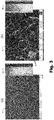
- Fig. 3(a) shows a scanning electron microscope (SEM) image 22 and photograph 24 of the pure CS Cu sample.
- the copper powder used for cold spraying had a particle size of 10-60 ⁇ m. It is clear that is it more-or-less continuous Cu, and this is verified by a density measurement which was found to be that of pure Cu, within experimental uncertainty ( ⁇ 5%). This is further verified by the thermal conductivity measurement of the CS 0% Diamond sample shown in Fig. 2 , which shows that it is that of pure Cu, within experimental uncertainty ( ⁇ 10%).
- Fig. 3(b) shows a SEM image 26 and photograph 28 of a CS 30% Diamond grit ( ⁇ 100 ⁇ m) Cu-Diamond composite. A diamond particle is highlighted and indicated at 30.
- the thermal conductivity measurement together with the density measurement (which was used to estimate ⁇ d) not only verify that the diamond particles are present and participating positively with regard to thermal conductivity of the composite, but the close agreement with Maxwell's theory strongly suggests that the CS fabrication technique forms a composite with a low Cu-Diamond interfacial thermal barrier.
- Fig. 4 is a schematic diagram of a cold spraying apparatus used to create the structures described herein.
- a pressurised gas source 30 feeds the apparatus and is split into two streams.
- An upper stream passes by and picks up powder particles from a powder feeder 32.
- the lower stream passes through a gas heater 34 to increase the gas temperature, hence sonic speed, hence actual velocity at the nozzle exit, before the heated gas stream and the stream carrying the entrained powder particles are reunited.
- the reunited gas stream and the entrained particles pass through a supersonic nozzle 36 which accelerates the particles to impact a substrate 38.
- the particles deform plastically and adhere to the substrate and one another to provide a deposited layer 40 whose thickness and shape can be controlled by moving the substrate relative to the deposition point and by varying gas temperature, the gas pressure and composition, the relative flow rates through the upper and lower branches and so on.
- the structure of the deposited layer can be varied by the choice of powdered material (or mix of powders) and the particle size distribution.
- the preferred top layer is a matrix of copper with embedded diamond, and the most commercially important substrate is silicon, tests were performed on CS copper layers deposited on silicon substrates.
- a 30 ⁇ m copper layer was deposited on silicon, and adhesive strength measured with a tape test in which Scotch Klebeband pressure sensitive tape was applied to the deposited copper layer and the tape was then pulled away, to see if the copper came away with the tape or remained fixed on the silicon (Scotch Klebeband is a trade mark of 3M Corporation).
- Fig. 7 shows a cold sprayed layer 58 formed from 30 ⁇ m aluminium powder on silicon. Unlike 30 ⁇ m copper the aluminium bonds strongly to the silicon, and passes the tape test. Furthermore, it has none of the material handling drawbacks of the 1 ⁇ m copper, and it also is robust enough to permit additional layers to be built on top.
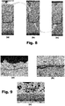
- Fig. 8 shows a three-layer structure on top of silicon.
- a base layer is formed by cold spraying 30 ⁇ m (average particle size) aluminium.
- an intermediate layer is formed by cold spraying 30 ⁇ m copper.
- a copper diamond matrix top layer is formed by cold spraying a mixture of 30 ⁇ m copper and 80 ⁇ m diamond powder.
- Figs 9(a) to 9(c) are SEM micrographs through the three samples of Figs. 8(a) to 8(c) respectively.
- the magnitude of Fig. 9(a) is incidentally twice that of Figs. 9(b) and 9(c) , i.e. a length scale marker in the lower left side of each indicates a length of 0.250mm in 9(a) and the corresponding scale markers indicate lengths of 0.504mm and 0.506mm in 9(b) and (c) respectively.
- Fig. 10 provides a more detailed SEM cross section through the finished structure, with details magnified of a diamond particle (i), the Cu-AI interface (ii), and the Al-Si interface (iii).
- the top surface formed using cold spray is far from smooth at a microscopic level.
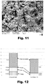
- Fig. 11 is a SEM micrograph of the top surface taken from above, and it reveals numerous bumps, hollows and surface features.
- Surface feature analysis shows that the areal roughness parameters of this surface have the following values: Sa (average of absolute profile heights measured over a unit surface in the XY plane):
- the finished surface is highly porous and irregular which is of significant benefit for a thermal dissipation surface and this makes the structure particularly suitable for cooling high-power electronic devices, particularly using liquid cooling techniques.
- wicking in the copper-diamond composite proving that there is porosity.
- the roughness and porosity of the upper part of the top layer can be increased further by varying the cold spray parameters to "disimprove" the deposition of the mixture in the final part of spraying, e.g. by reducing the feed rate of powder, translating the workpiece more quickly relative to the stream of particles, or adjusting other variables in the process.
- a significant advantage of the structures disclosed herein is that they can be created in a single continuous cold spraying process to build up the various CS layers onto the semiconductor substrate, making this a fast and inexpensive method of manufacturing a high-performance thermal dissipation structure.
- Fig. 12 is a comparison of the thermal resistance budgets for the conventional design of Fig. 1 (left-hand column in Fig. 12 ) and for a thermal structure comprising an integrated heat spreader formed of a copper-diamond cold-sprayed layer deposited directly onto silicon (right-hand column).
- the thermal resistance budget for the conventional design is 0.68 K/W, which arises from the consecutive components (starting from the silicon surface) of the TIM 1 layer (0.111), integrated heat spreader (IHS) of copper (0.124), TIM 2 layer (0.025) and a fan-fin heat sink (0.42).
- the novel design has a thermal resistance of 0.496, made up of an IHS of cold sprayed copper-diamond (0.051), and the same values for the TIM 2 layer and the heat sink. Because of the reduced value for the IHS, and the elimination of a TIM 1 layer, the thermal resistance is reduced by almost 30%. This translates to a 15°C junction temperature drop at the thermal design power.
- the above figures are based on a chip having dimensions of 15 mm by 15 mm, onto which an AI layer is cold sprayed using particles of 30 ⁇ m, to a thickness of 75 ⁇ m, before a 40:60 powder mixture of 30 ⁇ m copper and 30 ⁇ m diamond is cold sprayed to a thickness of 2.5 mm.
- the base layer shown and described in the embodiments above need not be aluminium and some further examples below provide alternative base layers.
- the copper intermediate layer is optional.
- the aluminium base layer is formed by electro deposition. This could be varied further by using physical or chemical vapour deposition (PVD or CVD), os using some other technique. It is however important to ensure that whatever deposition or formation method is employed, the base layer is in intimate contact with the substrate and has a high degree of continuity so that an efficient thermal transfer is provided through the base layer from the substrate to the top layer.
- PVD physical or chemical vapour deposition
- a copper base layer was substituted for the aluminium base layer of example 1.
- the copper base layer was cold sprayed using 1 ⁇ m copper particles.
- Fig. 13 shows a photograph of an experimental test where a track of 1 ⁇ m copper powder 60 is cold sprayed onto a silicon wafer 62. Adhesive strength was measured with a tape test in which Scotch Klebeband pressure sensitive tape was applied to the deposited copper layer and the tape was then pulled away, to see if the copper came away with the tape or remained fixed on the silicon (Scotch Klebeband is a trade mark of 3M Corporation). It was found that the copper bonded strongly and did not come away.
- the particle size used could be smaller or larger. It is preferred to use copper powder with an average size in the range 1-10 ⁇ m. The larger the particle, the easier it is to handle, but the more energy it imparts to the substrate on impact. The cold spray parameters will also influence the impact energy and different substrates will have different limits for impact energy to avoid fracture or damage.
- the copper base layer is deposited to 30 ⁇ m followed by cold spraying of the (optional) intermediate layer of copper and the top layer of copper-diamond.
- a minimum of 20 ⁇ m is preferred to withstand the impact of the cold sprayed particles onto the copper base layer.
- a thermal structure is formed with a base layer and top layer, with no intermediate layer. Both the base layer and top layer are formed from a copper-diamond matrix. As before a 30 ⁇ m copper and 80 ⁇ m diamond mix is used for the top layer. For the base layer, a 3 ⁇ m copper powder is mixed with a 5 ⁇ m diamond grit, and these are cold sprayed to build up a base layer which has good adhesion, excellent thermal characteristics and which shields the substrate when the top layer is sprayed on with a higher average incident particle energy.
- small (1-10 ⁇ m) copper-clad diamond particles could be substituted for the mix of small copper powder/diamond grit.
- the base layer is homogeneous with the top layer, both being formed in a continuous cold spraying process using the same 3 ⁇ m copper powder mixed with a 5 ⁇ m diamond grit.
- This example differs from the others in that it does not employ a distinct base layer but rather has a single layer with both base layer functionality and top layer functionality.
Landscapes
- Cooling Or The Like Of Semiconductors Or Solid State Devices (AREA)
- Chemical & Material Sciences (AREA)
- Engineering & Computer Science (AREA)
- Materials Engineering (AREA)
- Coating By Spraying Or Casting (AREA)
- Other Surface Treatments For Metallic Materials (AREA)
Claims (15)
- Thermische Struktur zur Ableitung von Wärme aus einem Substrat, umfassend:ein Halbleitersubstrat, das eine Außenfläche aufweist;eine Basisschicht eines duktilen Materials, das dazu in der Lage ist, plastische Verformung aufzuweisen, die auf der Außenfläche gebildet ist; undeine obere Schicht, die eine Matrix aus Metall und Diamant umfasst, die über der Basisschicht durch Kaltgasspritzen eines Pulvers, das aus Folgenden ausgewählt ist, gebildet wird:einer Pulvermischung aus Metall- und Diamantpartikeln; undeinem Pulver aus metallgekapselten Diamantpartikeln,wobei die obere Schicht aus einer Matrix aus Metall, die durch die Verformung der Metallkomponenten des Pulvers beim Aufprall auf die darunterliegenden Fläche gebildet wird, und einer dispergierten Phase, die die in der Metallmatrix eingebetteten Diamantpartikel umfasst, gebildet ist.
- Thermische Struktur nach Anspruch 1, wobei die Basisschicht auf der Außenfläche durch einen Kaltgasspritzvorgang gebildet wird, wobei die obere Schicht über der Basisschicht gebildet ist, wobei die Basisschicht aus (i) einem Metall; (ii) einem Verbundstoff, der mindestens zwei Metalle umfasst, oder (iii) einem Verbundstoff, der ein Metall und ein Nichtmetall umfasst, gebildet ist.
- Thermische Struktur nach Anspruch 1 oder 2, wobei die Basisschicht aus Aluminium oder aus einem Verbundstoff aus Aluminium und einer oder mehreren metallischen oder nicht metallischen Komponenten gebildet ist.
- Thermische Struktur nach Anspruch 1 oder 2, wobei die Basisschicht aus Kupfer, aus einem Verbundstoff aus Kupfer und einer oder mehreren metallischen oder nicht metallischen Komponenten gebildet ist.
- Thermische Struktur nach einem der Ansprüche 1-3, wobei die Basisschicht Aluminium und Kupfer umfasst und durch Kaltgasspritzen eines Gemisches aus Kupfer- und Aluminiumpartikeln gebildet wird.
- Thermische Struktur nach einem der vorangehenden Ansprüche, wobei die Außenfläche des Substrats vor der Bildung der Basisschicht durch einen Prozess ausgewählt aus chemischem Ätzen, Sandstrahlen und Laserätzen aufgeraut wird.
- Thermische Struktur nach einem der vorangehenden Ansprüche, wobei das Metall in der oberen Schicht Kupfer ist.
- Thermische Struktur nach einem der vorangehenden Ansprüche, wobei die obere Schicht ein Gemisch aus Kupfer und Diamant im Verhältnis (Gew./Gew.) von 30:70 und 90:10, bevorzugter zwischen 50:50 und 90:10, noch bevorzugter zwischen 75:25 und 90:10, am stärksten bevorzugt um 80:20 umfasst.
- Thermische Struktur nach einem der vorangehenden Ansprüche, wobei das Pulver ein Pulvergemisch aus Metall- und Diamantpartikeln ist und wobei die Metallpartikel eine durchschnittliche Größe von zwischen 10 und 60 µm aufweisen.
- Thermische Struktur nach einem der vorangehenden Ansprüche, wobei die Diamantpartikel in dem Gemisch oder in den metallgekapselten Metallpartikeln eine durchschnittliche Größe von zwischen 10 und 200 µm, bevorzugter zwischen 20 und 100 µm aufweisen.
- Thermische Struktur nach einem der Ansprüche 1-8, wobei das Pulver ein Pulver aus metallgekapselten Diamantpartikel ist, wobei das Metall Kupfer ist.
- Thermische Struktur nach einem der vorangehenden Ansprüche, ferner umfassend eine Zwischenschicht aus Kupfer, die auf der Basisschicht durch einen Kaltgasspritzvorgang gebildet wird, wobei die obere Schicht auf die Zwischenschicht kaltgasgespritzt wird.
- Thermische Struktur nach einem der vorangehenden Ansprüche, wobei die obere Schicht an der Außenfläche distal von dem Substrat mit multiskalaren Merkmalen relativ zu der Masse der oberen Schichtmit einer bevorzugten Merkmalsgröße zwischen 0,5 µm und 120 µm breitgestellt ist.
- Thermische Struktur nach Anspruch 13, wobei die erhöhte Porosität aus einer Variation der Kaltgasspritzparameter während des Aufbringens des äußersten Teils der oberen Schicht durch eines oder mehrere von Folgenden resultiert: Variieren des Düseneinlassdrucks, des Arbeitsabstands, der Partikelzufuhrrate und der relativen Bewegung zwischen Substrat und Düse.
- Verfahren zur Herstellung einer thermischen Struktur zur Ableitung von Wärme aus einem Substrat, umfassend die folgenden Schritte:Bereitstellen eines Halbleitersubstrats, das eine Außenfläche aufweist; undBilden einer Basisschicht aus duktilem Material, das dazu in der Lage ist, eine plastische Verformung aufzuweisen, auf der Außenfläche; undBilden einer oberen Schicht über der Basisschicht durch Kaltgasspritzen eines Pulvers ausgewählt aus:einem Pulvergemisch aus Metall- und Diamantpartikeln undeinem Pulver aus metallgekapselten Diamantpartikeln;wobei eine Matrix aus Metall durch die Verformung der Metallpartikel beim Aufprall auf die darunterliegende Fläche gebildet wird und eine dispergierte Phase, die die Diamantpartikel umfasst, in die Metallmatrix eingebettet wird.
Applications Claiming Priority (2)
| Application Number | Priority Date | Filing Date | Title |
|---|---|---|---|
| EP17189219.3A EP3451376A1 (de) | 2017-09-04 | 2017-09-04 | Thermische strukturen zur ableitung von wärme und verfahren zur herstellung davon |
| PCT/EP2018/073785 WO2019043269A1 (en) | 2017-09-04 | 2018-09-04 | THERMAL STRUCTURES FOR DISSIPATING HEAT AND METHODS OF MAKING SAME |
Publications (2)
| Publication Number | Publication Date |
|---|---|
| EP3679602A1 EP3679602A1 (de) | 2020-07-15 |
| EP3679602B1 true EP3679602B1 (de) | 2021-08-25 |
Family
ID=59790966
Family Applications (2)
| Application Number | Title | Priority Date | Filing Date |
|---|---|---|---|
| EP17189219.3A Withdrawn EP3451376A1 (de) | 2017-09-04 | 2017-09-04 | Thermische strukturen zur ableitung von wärme und verfahren zur herstellung davon |
| EP18759976.6A Active EP3679602B1 (de) | 2017-09-04 | 2018-09-04 | Thermische strukturen zur ableitung von wärme und verfahren zur herstellung davon |
Family Applications Before (1)
| Application Number | Title | Priority Date | Filing Date |
|---|---|---|---|
| EP17189219.3A Withdrawn EP3451376A1 (de) | 2017-09-04 | 2017-09-04 | Thermische strukturen zur ableitung von wärme und verfahren zur herstellung davon |
Country Status (5)
| Country | Link |
|---|---|
| US (1) | US11158560B2 (de) |
| EP (2) | EP3451376A1 (de) |
| KR (1) | KR102551453B1 (de) |
| CN (1) | CN111164747B (de) |
| WO (1) | WO2019043269A1 (de) |
Families Citing this family (14)
| Publication number | Priority date | Publication date | Assignee | Title |
|---|---|---|---|---|
| US9335296B2 (en) | 2012-10-10 | 2016-05-10 | Westinghouse Electric Company Llc | Systems and methods for steam generator tube analysis for detection of tube degradation |
| WO2019163721A1 (ja) * | 2018-02-21 | 2019-08-29 | 住友電気工業株式会社 | 複合材料、及び複合材料の製造方法 |
| US11935662B2 (en) | 2019-07-02 | 2024-03-19 | Westinghouse Electric Company Llc | Elongate SiC fuel elements |
| ES2955292T3 (es) | 2019-09-19 | 2023-11-29 | Westinghouse Electric Co Llc | Aparato para realizar pruebas de adherencia in situ de depósitos de pulverización en frío y procedimiento de empleo |
| CN111826542B (zh) * | 2020-06-30 | 2022-01-04 | 长沙新材料产业研究院有限公司 | 一种铜基金刚石梯度散热材料及其制备方法 |
| CN112701561B (zh) * | 2020-12-30 | 2022-02-22 | 深圳市利拓光电有限公司 | 高速25g半导体激光器芯片的封装结构及封装方法 |
| EP4317528A4 (de) | 2021-04-02 | 2024-10-02 | Hojitsu Seiko Co., Ltd. | Keramisches beschichtungselement |
| TWI760269B (zh) * | 2021-07-30 | 2022-04-01 | 宏進金屬科技股份有限公司 | 散熱片之製法 |
| US20230160646A1 (en) * | 2021-11-19 | 2023-05-25 | Amulaire Thermal Technology, Inc. | Immersion heat dissipation structure |
| KR102866116B1 (ko) | 2021-11-26 | 2025-09-30 | 삼성전자주식회사 | 반도체 패키지 |
| CN116586610A (zh) * | 2023-05-29 | 2023-08-15 | 江西省科学院应用物理研究所 | 一种金刚石增强铜基材料及其制备方法和应用 |
| CN119419123B (zh) * | 2024-10-17 | 2025-10-24 | 乐山希尔电子股份有限公司 | 一种导热导电功率模块的制备工艺 |
| CN119640266B (zh) * | 2024-11-29 | 2025-08-12 | 江苏富乐华半导体科技股份有限公司 | 一种封装用覆铝氮化铝陶瓷基板及其制备方法 |
| CN120709152B (zh) * | 2025-08-27 | 2025-10-28 | 无锡市乾野微纳科技有限公司 | Wlcsp芯片的多dbc封装结构及封装方法 |
Family Cites Families (10)
| Publication number | Priority date | Publication date | Assignee | Title |
|---|---|---|---|---|
| US6727117B1 (en) * | 2002-11-07 | 2004-04-27 | Kyocera America, Inc. | Semiconductor substrate having copper/diamond composite material and method of making same |
| KR100802329B1 (ko) * | 2005-04-15 | 2008-02-13 | 주식회사 솔믹스 | 금속기지 복합체 형성방법 및 이를 이용하여 제조된 코팅층및 벌크 |
| CN101126135B (zh) * | 2007-09-11 | 2010-07-21 | 西安交通大学 | 纳米金属陶瓷基金属陶瓷的制备方法 |
| WO2012147610A1 (ja) * | 2011-04-28 | 2012-11-01 | 株式会社アライドマテリアル | 放熱基板 |
| TW201342423A (zh) * | 2012-04-13 | 2013-10-16 | 國立交通大學 | 散熱基板與其製作方法 |
| WO2015047545A1 (en) * | 2013-09-27 | 2015-04-02 | United Technologies Corporation | Self-peening feedstock materials for cold spray deposition |
| CN104018156B (zh) * | 2014-06-18 | 2017-07-28 | 浙江工业大学 | 一种金属基/金刚石激光复合涂层及其制备方法 |
| US10539379B2 (en) * | 2014-09-02 | 2020-01-21 | Denka Company Limited | Heat dissipation component for semiconductor element |
| CN104878343B (zh) * | 2015-05-18 | 2018-07-20 | 广东省新材料研究所 | 一种金刚石/铜复合材料表面纯铜涂层制备方法 |
| US10751912B2 (en) * | 2015-10-13 | 2020-08-25 | Denka Company Limited | Aluminum-diamond-based composite and method for producing same |
-
2017
- 2017-09-04 EP EP17189219.3A patent/EP3451376A1/de not_active Withdrawn
-
2018
- 2018-09-04 US US16/644,297 patent/US11158560B2/en active Active
- 2018-09-04 KR KR1020207007717A patent/KR102551453B1/ko active Active
- 2018-09-04 WO PCT/EP2018/073785 patent/WO2019043269A1/en not_active Ceased
- 2018-09-04 EP EP18759976.6A patent/EP3679602B1/de active Active
- 2018-09-04 CN CN201880060468.6A patent/CN111164747B/zh active Active
Also Published As
| Publication number | Publication date |
|---|---|
| EP3451376A1 (de) | 2019-03-06 |
| EP3679602A1 (de) | 2020-07-15 |
| US11158560B2 (en) | 2021-10-26 |
| KR20200052301A (ko) | 2020-05-14 |
| KR102551453B1 (ko) | 2023-07-04 |
| WO2019043269A1 (en) | 2019-03-07 |
| CN111164747B (zh) | 2023-12-05 |
| CN111164747A (zh) | 2020-05-15 |
| US20200194334A1 (en) | 2020-06-18 |
Similar Documents
| Publication | Publication Date | Title |
|---|---|---|
| US11158560B2 (en) | Thermal structures for dissipating heat and methods for manufacture thereof | |
| US10785862B2 (en) | Microelectronic modules with sinter-bonded heat dissipation structures and methods for the fabrication thereof | |
| Chen et al. | Mechanical deformation of sintered porous Ag die attach at high temperature and its size effect for wide-bandgap power device design | |
| Che et al. | Spark plasma sintering of titanium-coated diamond and copper–titanium powder to enhance thermal conductivity of diamond/copper composites | |
| EP3190613B1 (de) | Wärmeableitungselement und verfahren zur herstellung des wärmeableitungselements | |
| KR101115865B1 (ko) | 성막 방법, 전열 부재, 파워 모듈, 차량용 인버터, 및 차량 | |
| US12482779B2 (en) | Hybrid backside thermal structures for enhanced ic packages | |
| CN106129025B (zh) | 电子装置及其制法 | |
| US9024436B2 (en) | Thermal interface material for integrated circuit package | |
| US9984951B2 (en) | Sintered multilayer heat sinks for microelectronic packages and methods for the production thereof | |
| Guillemet et al. | An innovative process to fabricate copper/diamond composite films for thermal management applications | |
| CN100454525C (zh) | 复合材料及电路或电模块 | |
| EP3588553A1 (de) | Mikroelektronische module mit thermischen erweiterungsstufen und verfahren zur herstellung davon | |
| WO2016033522A1 (en) | Conductive bond foils | |
| GB2549499A (en) | Method of forming a heat exchanger | |
| JP6962803B2 (ja) | クラッド材およびその製造方法 | |
| CN110957228A (zh) | 一种碳化硅表面增强的铝散热基板及制造方法 | |
| US20210410331A1 (en) | Integrated circuit die thermal solutions with a contiguously integrated heat pipe | |
| Davidson et al. | Copper-diamond composite substrates for electronic components | |
| TW201306195A (zh) | 散熱基板 | |
| US12482719B2 (en) | Low-stress thermal interface | |
| Mistrini et al. | Laser Powder Bed Fusion of Sn-Al Multimaterial Pin-Fin Heat Sinks on Silicon Wafer for Electronic Heat Dissipation |
Legal Events
| Date | Code | Title | Description |
|---|---|---|---|
| STAA | Information on the status of an ep patent application or granted ep patent |
Free format text: STATUS: UNKNOWN |
|
| STAA | Information on the status of an ep patent application or granted ep patent |
Free format text: STATUS: THE INTERNATIONAL PUBLICATION HAS BEEN MADE |
|
| PUAI | Public reference made under article 153(3) epc to a published international application that has entered the european phase |
Free format text: ORIGINAL CODE: 0009012 |
|
| STAA | Information on the status of an ep patent application or granted ep patent |
Free format text: STATUS: REQUEST FOR EXAMINATION WAS MADE |
|
| 17P | Request for examination filed |
Effective date: 20200313 |
|
| AK | Designated contracting states |
Kind code of ref document: A1 Designated state(s): AL AT BE BG CH CY CZ DE DK EE ES FI FR GB GR HR HU IE IS IT LI LT LU LV MC MK MT NL NO PL PT RO RS SE SI SK SM TR |
|
| AX | Request for extension of the european patent |
Extension state: BA ME |
|
| DAV | Request for validation of the european patent (deleted) | ||
| DAX | Request for extension of the european patent (deleted) | ||
| GRAP | Despatch of communication of intention to grant a patent |
Free format text: ORIGINAL CODE: EPIDOSNIGR1 |
|
| STAA | Information on the status of an ep patent application or granted ep patent |
Free format text: STATUS: GRANT OF PATENT IS INTENDED |
|
| INTG | Intention to grant announced |
Effective date: 20210504 |
|
| GRAS | Grant fee paid |
Free format text: ORIGINAL CODE: EPIDOSNIGR3 |
|
| GRAA | (expected) grant |
Free format text: ORIGINAL CODE: 0009210 |
|
| STAA | Information on the status of an ep patent application or granted ep patent |
Free format text: STATUS: THE PATENT HAS BEEN GRANTED |
|
| AK | Designated contracting states |
Kind code of ref document: B1 Designated state(s): AL AT BE BG CH CY CZ DE DK EE ES FI FR GB GR HR HU IE IS IT LI LT LU LV MC MK MT NL NO PL PT RO RS SE SI SK SM TR |
|
| REG | Reference to a national code |
Ref country code: CH Ref legal event code: EP |
|
| REG | Reference to a national code |
Ref country code: IE Ref legal event code: FG4D Ref country code: AT Ref legal event code: REF Ref document number: 1424677 Country of ref document: AT Kind code of ref document: T Effective date: 20210915 |
|
| REG | Reference to a national code |
Ref country code: DE Ref legal event code: R096 Ref document number: 602018022495 Country of ref document: DE |
|
| REG | Reference to a national code |
Ref country code: LT Ref legal event code: MG9D |
|
| REG | Reference to a national code |
Ref country code: NL Ref legal event code: FP |
|
| REG | Reference to a national code |
Ref country code: AT Ref legal event code: MK05 Ref document number: 1424677 Country of ref document: AT Kind code of ref document: T Effective date: 20210825 |
|
| PG25 | Lapsed in a contracting state [announced via postgrant information from national office to epo] |
Ref country code: RS Free format text: LAPSE BECAUSE OF FAILURE TO SUBMIT A TRANSLATION OF THE DESCRIPTION OR TO PAY THE FEE WITHIN THE PRESCRIBED TIME-LIMIT Effective date: 20210825 Ref country code: SE Free format text: LAPSE BECAUSE OF FAILURE TO SUBMIT A TRANSLATION OF THE DESCRIPTION OR TO PAY THE FEE WITHIN THE PRESCRIBED TIME-LIMIT Effective date: 20210825 Ref country code: HR Free format text: LAPSE BECAUSE OF FAILURE TO SUBMIT A TRANSLATION OF THE DESCRIPTION OR TO PAY THE FEE WITHIN THE PRESCRIBED TIME-LIMIT Effective date: 20210825 Ref country code: ES Free format text: LAPSE BECAUSE OF FAILURE TO SUBMIT A TRANSLATION OF THE DESCRIPTION OR TO PAY THE FEE WITHIN THE PRESCRIBED TIME-LIMIT Effective date: 20210825 Ref country code: FI Free format text: LAPSE BECAUSE OF FAILURE TO SUBMIT A TRANSLATION OF THE DESCRIPTION OR TO PAY THE FEE WITHIN THE PRESCRIBED TIME-LIMIT Effective date: 20210825 Ref country code: LT Free format text: LAPSE BECAUSE OF FAILURE TO SUBMIT A TRANSLATION OF THE DESCRIPTION OR TO PAY THE FEE WITHIN THE PRESCRIBED TIME-LIMIT Effective date: 20210825 Ref country code: BG Free format text: LAPSE BECAUSE OF FAILURE TO SUBMIT A TRANSLATION OF THE DESCRIPTION OR TO PAY THE FEE WITHIN THE PRESCRIBED TIME-LIMIT Effective date: 20211125 Ref country code: AT Free format text: LAPSE BECAUSE OF FAILURE TO SUBMIT A TRANSLATION OF THE DESCRIPTION OR TO PAY THE FEE WITHIN THE PRESCRIBED TIME-LIMIT Effective date: 20210825 Ref country code: NO Free format text: LAPSE BECAUSE OF FAILURE TO SUBMIT A TRANSLATION OF THE DESCRIPTION OR TO PAY THE FEE WITHIN THE PRESCRIBED TIME-LIMIT Effective date: 20211125 Ref country code: PT Free format text: LAPSE BECAUSE OF FAILURE TO SUBMIT A TRANSLATION OF THE DESCRIPTION OR TO PAY THE FEE WITHIN THE PRESCRIBED TIME-LIMIT Effective date: 20211227 |
|
| PG25 | Lapsed in a contracting state [announced via postgrant information from national office to epo] |
Ref country code: PL Free format text: LAPSE BECAUSE OF FAILURE TO SUBMIT A TRANSLATION OF THE DESCRIPTION OR TO PAY THE FEE WITHIN THE PRESCRIBED TIME-LIMIT Effective date: 20210825 Ref country code: LV Free format text: LAPSE BECAUSE OF FAILURE TO SUBMIT A TRANSLATION OF THE DESCRIPTION OR TO PAY THE FEE WITHIN THE PRESCRIBED TIME-LIMIT Effective date: 20210825 Ref country code: GR Free format text: LAPSE BECAUSE OF FAILURE TO SUBMIT A TRANSLATION OF THE DESCRIPTION OR TO PAY THE FEE WITHIN THE PRESCRIBED TIME-LIMIT Effective date: 20211126 |
|
| PG25 | Lapsed in a contracting state [announced via postgrant information from national office to epo] |
Ref country code: DK Free format text: LAPSE BECAUSE OF FAILURE TO SUBMIT A TRANSLATION OF THE DESCRIPTION OR TO PAY THE FEE WITHIN THE PRESCRIBED TIME-LIMIT Effective date: 20210825 |
|
| REG | Reference to a national code |
Ref country code: CH Ref legal event code: PL |
|
| REG | Reference to a national code |
Ref country code: BE Ref legal event code: MM Effective date: 20210930 |
|
| REG | Reference to a national code |
Ref country code: DE Ref legal event code: R097 Ref document number: 602018022495 Country of ref document: DE |
|
| PG25 | Lapsed in a contracting state [announced via postgrant information from national office to epo] |
Ref country code: SM Free format text: LAPSE BECAUSE OF FAILURE TO SUBMIT A TRANSLATION OF THE DESCRIPTION OR TO PAY THE FEE WITHIN THE PRESCRIBED TIME-LIMIT Effective date: 20210825 Ref country code: SK Free format text: LAPSE BECAUSE OF FAILURE TO SUBMIT A TRANSLATION OF THE DESCRIPTION OR TO PAY THE FEE WITHIN THE PRESCRIBED TIME-LIMIT Effective date: 20210825 Ref country code: RO Free format text: LAPSE BECAUSE OF FAILURE TO SUBMIT A TRANSLATION OF THE DESCRIPTION OR TO PAY THE FEE WITHIN THE PRESCRIBED TIME-LIMIT Effective date: 20210825 Ref country code: MC Free format text: LAPSE BECAUSE OF FAILURE TO SUBMIT A TRANSLATION OF THE DESCRIPTION OR TO PAY THE FEE WITHIN THE PRESCRIBED TIME-LIMIT Effective date: 20210825 Ref country code: EE Free format text: LAPSE BECAUSE OF FAILURE TO SUBMIT A TRANSLATION OF THE DESCRIPTION OR TO PAY THE FEE WITHIN THE PRESCRIBED TIME-LIMIT Effective date: 20210825 Ref country code: CZ Free format text: LAPSE BECAUSE OF FAILURE TO SUBMIT A TRANSLATION OF THE DESCRIPTION OR TO PAY THE FEE WITHIN THE PRESCRIBED TIME-LIMIT Effective date: 20210825 Ref country code: AL Free format text: LAPSE BECAUSE OF FAILURE TO SUBMIT A TRANSLATION OF THE DESCRIPTION OR TO PAY THE FEE WITHIN THE PRESCRIBED TIME-LIMIT Effective date: 20210825 |
|
| PLBE | No opposition filed within time limit |
Free format text: ORIGINAL CODE: 0009261 |
|
| STAA | Information on the status of an ep patent application or granted ep patent |
Free format text: STATUS: NO OPPOSITION FILED WITHIN TIME LIMIT |
|
| PG25 | Lapsed in a contracting state [announced via postgrant information from national office to epo] |
Ref country code: LU Free format text: LAPSE BECAUSE OF NON-PAYMENT OF DUE FEES Effective date: 20210904 Ref country code: IT Free format text: LAPSE BECAUSE OF FAILURE TO SUBMIT A TRANSLATION OF THE DESCRIPTION OR TO PAY THE FEE WITHIN THE PRESCRIBED TIME-LIMIT Effective date: 20210825 Ref country code: BE Free format text: LAPSE BECAUSE OF NON-PAYMENT OF DUE FEES Effective date: 20210930 |
|
| 26N | No opposition filed |
Effective date: 20220527 |
|
| PG25 | Lapsed in a contracting state [announced via postgrant information from national office to epo] |
Ref country code: SI Free format text: LAPSE BECAUSE OF FAILURE TO SUBMIT A TRANSLATION OF THE DESCRIPTION OR TO PAY THE FEE WITHIN THE PRESCRIBED TIME-LIMIT Effective date: 20210825 Ref country code: LI Free format text: LAPSE BECAUSE OF NON-PAYMENT OF DUE FEES Effective date: 20210930 Ref country code: CH Free format text: LAPSE BECAUSE OF NON-PAYMENT OF DUE FEES Effective date: 20210930 |
|
| GBPC | Gb: european patent ceased through non-payment of renewal fee |
Effective date: 20220904 |
|
| P01 | Opt-out of the competence of the unified patent court (upc) registered |
Effective date: 20230517 |
|
| PG25 | Lapsed in a contracting state [announced via postgrant information from national office to epo] |
Ref country code: CY Free format text: LAPSE BECAUSE OF FAILURE TO SUBMIT A TRANSLATION OF THE DESCRIPTION OR TO PAY THE FEE WITHIN THE PRESCRIBED TIME-LIMIT Effective date: 20210825 |
|
| PG25 | Lapsed in a contracting state [announced via postgrant information from national office to epo] |
Ref country code: HU Free format text: LAPSE BECAUSE OF FAILURE TO SUBMIT A TRANSLATION OF THE DESCRIPTION OR TO PAY THE FEE WITHIN THE PRESCRIBED TIME-LIMIT; INVALID AB INITIO Effective date: 20180904 |
|
| PG25 | Lapsed in a contracting state [announced via postgrant information from national office to epo] |
Ref country code: GB Free format text: LAPSE BECAUSE OF NON-PAYMENT OF DUE FEES Effective date: 20220904 |
|
| PG25 | Lapsed in a contracting state [announced via postgrant information from national office to epo] |
Ref country code: MK Free format text: LAPSE BECAUSE OF FAILURE TO SUBMIT A TRANSLATION OF THE DESCRIPTION OR TO PAY THE FEE WITHIN THE PRESCRIBED TIME-LIMIT Effective date: 20210825 |
|
| PG25 | Lapsed in a contracting state [announced via postgrant information from national office to epo] |
Ref country code: MT Free format text: LAPSE BECAUSE OF FAILURE TO SUBMIT A TRANSLATION OF THE DESCRIPTION OR TO PAY THE FEE WITHIN THE PRESCRIBED TIME-LIMIT Effective date: 20210825 |
|
| PGFP | Annual fee paid to national office [announced via postgrant information from national office to epo] |
Ref country code: IE Payment date: 20240801 Year of fee payment: 7 Ref country code: DE Payment date: 20240919 Year of fee payment: 7 |
|
| PGFP | Annual fee paid to national office [announced via postgrant information from national office to epo] |
Ref country code: FR Payment date: 20240924 Year of fee payment: 7 |
|
| PGFP | Annual fee paid to national office [announced via postgrant information from national office to epo] |
Ref country code: NL Payment date: 20240920 Year of fee payment: 7 |
|
| REG | Reference to a national code |
Ref country code: DE Ref legal event code: R079 Ref document number: 602018022495 Country of ref document: DE Free format text: PREVIOUS MAIN CLASS: H01L0023373000 Ipc: H10W0040250000 |
|
| PG25 | Lapsed in a contracting state [announced via postgrant information from national office to epo] |
Ref country code: TR Free format text: LAPSE BECAUSE OF FAILURE TO SUBMIT A TRANSLATION OF THE DESCRIPTION OR TO PAY THE FEE WITHIN THE PRESCRIBED TIME-LIMIT Effective date: 20210825 |
|
| REG | Reference to a national code |
Ref country code: NL Ref legal event code: MM Effective date: 20251001 |