EP3678052A1 - Fingerabdrucksensor und anzeigevorrichtung damit - Google Patents
Fingerabdrucksensor und anzeigevorrichtung damit Download PDFInfo
- Publication number
- EP3678052A1 EP3678052A1 EP20150196.2A EP20150196A EP3678052A1 EP 3678052 A1 EP3678052 A1 EP 3678052A1 EP 20150196 A EP20150196 A EP 20150196A EP 3678052 A1 EP3678052 A1 EP 3678052A1
- Authority
- EP
- European Patent Office
- Prior art keywords
- areas
- photo sensors
- disposed
- phs
- sensing lines
- Prior art date
- Legal status (The legal status is an assumption and is not a legal conclusion. Google has not performed a legal analysis and makes no representation as to the accuracy of the status listed.)
- Granted
Links
Images







Classifications
-
- G—PHYSICS
- G06—COMPUTING OR CALCULATING; COUNTING
- G06V—IMAGE OR VIDEO RECOGNITION OR UNDERSTANDING
- G06V40/00—Recognition of biometric, human-related or animal-related patterns in image or video data
- G06V40/10—Human or animal bodies, e.g. vehicle occupants or pedestrians; Body parts, e.g. hands
- G06V40/12—Fingerprints or palmprints
- G06V40/13—Sensors therefor
- G06V40/1318—Sensors therefor using electro-optical elements or layers, e.g. electroluminescent sensing
-
- G—PHYSICS
- G06—COMPUTING OR CALCULATING; COUNTING
- G06V—IMAGE OR VIDEO RECOGNITION OR UNDERSTANDING
- G06V10/00—Arrangements for image or video recognition or understanding
- G06V10/10—Image acquisition
- G06V10/12—Details of acquisition arrangements; Constructional details thereof
- G06V10/14—Optical characteristics of the device performing the acquisition or on the illumination arrangements
- G06V10/147—Details of sensors, e.g. sensor lenses
-
- G—PHYSICS
- G09—EDUCATION; CRYPTOGRAPHY; DISPLAY; ADVERTISING; SEALS
- G09F—DISPLAYING; ADVERTISING; SIGNS; LABELS OR NAME-PLATES; SEALS
- G09F9/00—Indicating arrangements for variable information in which the information is built-up on a support by selection or combination of individual elements
-
- H—ELECTRICITY
- H10—SEMICONDUCTOR DEVICES; ELECTRIC SOLID-STATE DEVICES NOT OTHERWISE PROVIDED FOR
- H10F—INORGANIC SEMICONDUCTOR DEVICES SENSITIVE TO INFRARED RADIATION, LIGHT, ELECTROMAGNETIC RADIATION OF SHORTER WAVELENGTH OR CORPUSCULAR RADIATION
- H10F39/00—Integrated devices, or assemblies of multiple devices, comprising at least one element covered by group H10F30/00, e.g. radiation detectors comprising photodiode arrays
- H10F39/80—Constructional details of image sensors
- H10F39/802—Geometry or disposition of elements in pixels, e.g. address-lines or gate electrodes
- H10F39/8023—Disposition of the elements in pixels, e.g. smaller elements in the centre of the imager compared to larger elements at the periphery
-
- H—ELECTRICITY
- H10—SEMICONDUCTOR DEVICES; ELECTRIC SOLID-STATE DEVICES NOT OTHERWISE PROVIDED FOR
- H10F—INORGANIC SEMICONDUCTOR DEVICES SENSITIVE TO INFRARED RADIATION, LIGHT, ELECTROMAGNETIC RADIATION OF SHORTER WAVELENGTH OR CORPUSCULAR RADIATION
- H10F39/00—Integrated devices, or assemblies of multiple devices, comprising at least one element covered by group H10F30/00, e.g. radiation detectors comprising photodiode arrays
- H10F39/80—Constructional details of image sensors
- H10F39/805—Coatings
- H10F39/8057—Optical shielding
-
- H—ELECTRICITY
- H10—SEMICONDUCTOR DEVICES; ELECTRIC SOLID-STATE DEVICES NOT OTHERWISE PROVIDED FOR
- H10K—ORGANIC ELECTRIC SOLID-STATE DEVICES
- H10K59/00—Integrated devices, or assemblies of multiple devices, comprising at least one organic light-emitting element covered by group H10K50/00
- H10K59/60—OLEDs integrated with inorganic light-sensitive elements, e.g. with inorganic solar cells or inorganic photodiodes
-
- H—ELECTRICITY
- H10—SEMICONDUCTOR DEVICES; ELECTRIC SOLID-STATE DEVICES NOT OTHERWISE PROVIDED FOR
- H10W—GENERIC PACKAGES, INTERCONNECTIONS, CONNECTORS OR OTHER CONSTRUCTIONAL DETAILS OF DEVICES COVERED BY CLASS H10
- H10W90/00—Package configurations
Definitions
- Exemplary embodiments of the inventive concept relate to a fingerprint sensor and a display device including the fingerprint sensor.
- Mobile devices such as smartphones and tablet personal computers include a locking function to prevent access by unauthorized users.
- the locking function include requiring the user to enter a password/pin, draw a certain shape, or apply their finger to a fingerprint sensor to unlock their device.
- a user may forget their password/pin or how to draw the shape.
- an unauthorized user can access their device if they are able to determine the password/pin or the shape.
- security of a mobile device can be greatly improved through use of the fingerprint sensor.
- a fingerprint sensor may be installed in or mounted to a display device of a mobile device to provide a fingerprint sensing function.
- the fingerprint sensor may be configured as an optical sensing type sensor.
- the optical sensing fingerprint sensor includes a light source and at least one photo sensor.
- photo sensors are used throughout a display panel of the display device, the production cost of the display device may be unnecessarily increased.
- Exemplary embodiments of the inventive concept are directed to an optical sensing fingerprint sensor capable of reducing the production cost of a display device, and a display device including the fingerprint sensor.
- Exemplary embodiments of the inventive concept are directed to a fingerprint sensor in which photo sensors are arranged in areas on a sensor layer at different resolutions, and a display device including the fingerprint sensor.
- An exemplary embodiment of the inventive concept provides a fingerprint sensor including: a first layer including a plurality of pixels; a light transmitting hole array layer including a plurality of light transmitting holes providing light transmitting paths of light rays that are incident through the first layer; and a sensor layer including a plurality of photo sensors configured to sense the light rays that pass through the light transmitting holes and are incident on the sensor layer, wherein a resolution at which the photo sensors are disposed in first areas on the sensor layer may differ from a resolution at which the photo sensors are disposed in second areas on the sensor layer.
- the photo sensors are disposed at a high resolution in the first areas and disposed at a low resolution in the second areas.
- a pitch between the photo sensors that are disposed in the second areas is greater than a pitch between the photo sensors that are disposed in the first areas.
- an area of each of the photo sensors that are disposed in the second areas is greater than an area of each of the photo sensors that are disposed in the first areas.
- the photo sensors are not disposed in the second areas.
- the first areas and the second areas form target areas on which the light rays passing through the light transmitting holes are incident.
- the first areas are respective central areas of the target areas
- the second areas are respective perimeter areas of the target areas other than the central areas.
- each of the first areas at least partially overlap with a corresponding one of the light transmitting holes.
- the target areas at least partially overlap with each other, and the second areas are areas in which the target areas overlap with each other.
- the target areas do not overlap with each other, and the sensor layer further includes third areas formed in areas of the sensor layer other than the target areas.
- a resolution at which the photo sensors are disposed in at least one of the first, second, and third areas differ from a resolution at which the photo sensors are disposed in at least one remaining areas thereof.
- a resolution at which the photo sensors are disposed in each of the third areas is equal to or lower than a resolution at which the photo sensors are disposed in each of the second areas.
- the photo sensors are not disposed in the third areas.
- the first layer includes: a circuit element layer including a plurality of circuit elements constituting a pixel circuit of each of the pixels; and a light emitting element layer on which light emitting elements for the pixels are located.
- the photo sensors are coupled both to first sensing lines configured to receive driving signals and to second sensing lines configured to output sensing signals in response to the sensed light rays.
- the number of photo sensors that are electrically coupled to a first group of first sensing lines is greater than the number of photo sensors that are electrically coupled to a second group of first sensing lines. In an exemplary embodiment, the number of photo sensors that are electrically coupled to a first group of the second sensing lines is greater than the number of photo sensors that are electrically coupled to a second group of the second sensing lines.
- the first group of first sensing lines and the first group of second sensing lines are electrically coupled to the photo sensors that are disposed in the first areas.
- the first group of first sensing lines and the first group of second sensing lines electrically couple any one of the photo sensors that are disposed in each of the first areas and any one of the photo sensors that are disposed in a corresponding one of the second areas.
- the first group of first sensing lines and the first group of second sensing lines is bent between any one of the photo sensors that are disposed in the first area and any one of the photo sensors that are disposed in the second area.
- An exemplary embodiment of the inventive concept provides a display device including: a display panel including a plurality of pixels and a light transmitting hole array layer including a plurality of light transmitting holes providing light transmitting paths of light rays that are incident from the outside; and a sensor layer disposed on one surface of the display panel and including a plurality of photo sensors configured to sense the light rays that are incident through the display panel, wherein a resolution at which the photo sensors are disposed in first areas on the sensor layer differs from a resolution at which the photo sensors are disposed in second areas on the sensor layer.
- the photo sensors are disposed at a high resolution in the first areas, and are disposed at a low resolution in the second areas or not disposed in the second areas.
- the first areas and the second areas form target areas on which the light rays passing through the light transmitting holes are incident.
- the first areas are respective central areas of the target areas and the second areas are respective perimeter areas of the target areas other than the central areas.
- the target areas at least partially overlap with each other, and the second areas are areas in which the target areas overlap with each other.
- the target areas do not overlap with each other and the sensor layer further includes third areas formed in areas of the sensor layer other than the target areas.
- a resolution at which the photo sensors are disposed in at least one of the first, second, and third areas differs from a resolution at which the photo sensors are disposed in at least one remaining areas thereof.
- the display device further includes a driving circuit and the pixels of the display device are coupled to scan lines and data lines.
- the driving circuit includes first through n-th scan drivers configured to supply scan signals to the pixels through the scan lines, a data driver configured to supply data signals and a bias signal to the pixels through the data lines, and a timing controller configured to supply image data and bias data to the data driver, and to sequentially supply first through nth start signals to the first through nth scan drivers, respectively.
- the pixels are supplied with the data signals when the scan signals are supplied during display periods, and are supplied with the bias signal when the scan signals are supplied during a bias period between the display periods, and n is a natural number greater than one.
- Exemplary embodiments of the inventive concept provide an optical sensing fingerprint sensor capable of reducing the production cost of a display device, and a display device including the fingerprint sensor.
- FIGS. 1 and 2 are diagrams schematically illustrating a display device 10 in accordance with an exemplary embodiment of the inventive concept.
- FIGS. 1 and 2 are diagrams schematically illustrating a display panel 110 and a driving circuit 200 for driving the display panel 110 that are provided in the display device 10 in accordance with an exemplary embodiment of the inventive concept.
- FIGS. 1 and 2 illustrate that the display panel 110 and the driving circuit 200 are separately provided, the inventive concept is not limited thereto.
- the entirety or portion of the driving circuit 200 may be integrally formed on the display panel 110.
- the display device 10 includes the display panel 110 and the driving circuit 200 configured to drive the display panel 110.
- the display panel 110 includes a display area AA and a non-display area NA.
- the display area AA is an area in which a plurality of pixels PXL are provided, and may be referred to as an active area.
- each of the pixels PXL include at least one light emitting element.
- the light emitting element could be an organic light emitting diode.
- the display device 10 may drive pixels PXL in response to image data input from an external device, thus displaying an image on the display area AA.
- the external device could be a data driving circuit.
- the display area AA includes a sensing area SA.
- the sensing area SA includes at least some of the pixels PXL provided in the display area AA.
- the entirety of the display area AA is set as the sensing area SA.
- FIG 1 illustrates an example where only one sensing area SA is formed on the display area AA
- the inventive concept is not limited thereto.
- a plurality of sensing areas SA arranged in a regular or irregular pattern may be formed on the display area AA.
- the plurality of sensing areas SA may have identical or different areas and shapes.
- FIG 1 illustrates an example where the sensing area SA is formed in at least a portion of the display area AA
- the inventive concept is not limited thereto.
- the display area AA and the sensing area SA may be provided to overlap with each other in only some area.
- a portion of the sensing area SA can overlap a portion of the non-display area NA while a remaining portion of the sensing area SA overlaps the display area AA.
- the non-display area NA may be an area disposed around the display area AA.
- the non-display area NA may be referred to as a non-active area.
- the non-display area NA comprehensively means any area of the display panel 110 except the display area AA.
- the non-display area NA includes, for example, a line area, a pad area, and various dummy areas.
- the line area may include signal lines such as scan lines, data lines, or sensing lines.
- the pad area may include conductive pads to connect to one of the signal lines and to another circuit element.
- the dummy area could include dummy pads that are not connected to any of the signal lines.
- the display device 10 further includes a plurality of photo sensors provided in the sensing area SA.
- the photo sensors PHS sense rays of light that are reflected by the finger of a user after being emitted from a light source, and analyze the rays of reflected light to sense the fingerprint of the user.
- the photo sensors PHS will be described as being used for fingerprint sensing by way of example, the photo sensors PHS may be used for a variety of purposes to perform various functions, e.g., as a touch sensor and a scanner.
- the photo sensors PHS are disposed on the sensing area SA.
- the photo sensors PHS may overlap with at least some or all of the pixels PXL provided on the sensing area SA, or may be disposed around the pixels PXL.
- at least some or all of the photo sensors PHS may be provided between the pixels PXL.
- a display device including photo sensors PHS overlapping some or all of the pixels PXL or including photo sensors PHS between the pixels may be referred to as a fingerprint sensor embedded display device when the photo sensors PHS are used to sense a fingerprint. Exemplary embodiments of the arrangement relationship between the photo sensors PHS and the pixels PXL will be described in more detail with reference to FIGS. 3A to 3E .
- the photo sensors PHS use, as a light source, a light emitting element provided in at least one pixel PXL which is disposed in or around the sensing area SA.
- the light emitting element could be an organic light emitting diode of a pixel.
- the photo sensors PHS, along with the pixels PXL of the sensing area SA, particularly, along with light emitting elements provided in the pixels PXL, may form a photo-sensing type fingerprint sensor.
- the fingerprint sensor embedded display device is configured using the pixels PXL as the light source without using a separate external light source, the thicknesses of the photo-sensing type fingerprint sensor and a portion of the display device that includes the fingerprint sensor may be reduced, and the production cost may also be reduced.
- the photo sensors PHS are disposed both on an image display surface (e.g., a front surface) of opposite surfaces of the display panel 110, and on the other surface (e.g., a rear surface) facing away the front surface.
- an image display surface e.g., a front surface
- the other surface e.g., a rear surface
- the inventive concept is not limited thereto.
- the display device 10 further includes an optical system for configuring the photo-sensing type fingerprint sensor along with the photo sensors PHS.
- the optical system may be formed integrally with the display panel 110.
- the display panel 110 may be an optical-system-integrated display panel including a pinhole array layer.
- the driving circuit 200 drives the display panel 110.
- the driving circuit 200 may output a data signal corresponding to image data to the display panel 110, or may output driving signals for the photo sensors PHS and receive sensing signals from the photo sensors PHS.
- the driving circuit 200 that has received the sensing signals may detect a shape of the fingerprint of the user based on the sensing signals.
- the driving circuit 200 includes a panel driving unit 210 (e.g., a panel driving circuit) and a fingerprint detection unit 220 (e.g., a fingerprint detection circuit).
- a panel driving unit 210 e.g., a panel driving circuit
- a fingerprint detection unit 220 e.g., a fingerprint detection circuit
- FIGS. 1 and 2 illustrate the panel driving unit 210 and the fingerprint detection unit 220 as being separately provided, the inventive concept is not limited thereto.
- at least portion of the fingerprint detection unit 220 may be integrated with the panel driving unit 210 or interlock with the panel driving unit 210.
- the panel driving unit 210 successively scans the pixels PXL of the display area AA and supplies data signals corresponding to image data to the pixels PXL.
- the display panel 110 may display an image corresponding to the image data.
- the panel driving unit 210 could activate a first row of the pixels PXL and apply data signals to the activated first row during a first period, activate a second row of the pixels PXL and apply data signals to the activated second row during a first period after the second period, .., and activate a last row of the pixels PXL and apply data signals to the activated last row during a last period.
- the panel driving unit 210 includes a scan driving circuit and data driving circuit (e.g., a data driver).
- the scan driving circuit may include a plurality of scan drivers (e.g., first through n-th scan drivers), one for each of the rows of pixels PXL.
- the pixels PXL may be coupled to scan lines and data lines.
- the scan drivers may be configured to supply scan signals to the pixels PXL through the scan lines.
- the data driver may be configured to supply data signals to the pixels PXL through the data lines. In an embodiment, the data driver supplies both the data signals and a bias signal to the pixels PXL through the data lines.
- the panel driving unit 210 may additionally include a timing control circuit (e.g., a timing controller).
- the timing controller may provide image data and bias data to the data driver.
- the data driver can generate data signals from the image data and bias signals from the bias data.
- the timing controller may sequentially supply first through n-th start signals to the first to n-th scan drivers.
- the start signals may indicate to a given scan driver when to start outputting a given one of the scan signals.
- the pixels PXL are supplied with the data signals when the scan signals are supplied during display periods, and are supplied with the bias signal when the scan signals are supplied during a bias period between the display periods.
- the panel driving unit 210 supplies driving signals for fingerprint sensing to the pixels PXL.
- the driving signals may be provided to cause the pixels PXL to emit light and operate as light sources for the photo sensors PHS.
- the driving signals for fingerprint sensing may be provided to pixels PXL provided in a specific area in the display panel 110, for example, to the pixels PXL provided in the sensing area SA.
- the driving signals for fingerprint sensing may be provided by the fingerprint detection unit 220.
- the fingerprint detection unit 220 may transmit driving signals for driving the photo sensors PHS to the photo sensors PHS, and detect the fingerprint of the user based on sensing signals received from the photo sensors PHS. For example, the sensing signals are received in response to transmitting the driving signals.
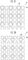
- FIGS. 3A to 3E are plan views illustrating exemplary embodiments of an arrangement structure of the pixels PXL and the photo sensors PHS in accordance with embodiments of the inventive concept.
- FIGS. 3A to 3E illustrate different exemplary embodiments pertaining to relative sizes, resolutions, and arrangement relationships between at least one or more pixels PXL and photo sensors PHS which are provided in the sensing area SA.
- the photo sensors PHS are disposed in the sensing area SA at the same resolution (or the same density) as that of the pixels PXL.
- the number of photo sensors PHS disposed in the sensing area SA is the same as that of the pixels PXL.
- the resolution may be in other words an area number density.
- the pixels PXL and the photo sensors PHS are disposed to be paired one-to-one with each other.
- the pixels PXL and the photo sensors PHS have been illustrated as overlapping with each other.
- the pixels PXL and the photo sensors PHS do not overlap with each other, or overlap with each other only in some area.
- each photo sensor PHS has been illustrated as having a size less than that of each pixel PXL, the inventive concept is not limited thereto.
- each photo sensor PHS may have a size equal to or greater than that of each pixel PXL. This exemplary embodiment is illustrated in FIGS 3C and 3D .
- the photo sensors PHS are disposed in the sensing area SA at a resolution lower than that of the pixels PXL. In other words, the number of photo sensors PHS disposed in the sensing area SA is less than that of the pixels PXL.
- FIGS. 3B to 3E illustrate examples in which one photo sensor PHS is disposed per four pixels PXL, the inventive concept is not limited thereto.
- each photo sensor PHS has a size less than that of each pixel PXL, or, as illustrated in FIGS. 3C and 3D , each photo sensor PHS has a size greater than that of each pixel PXL.
- the photo sensors PHS When the photo sensors PHS are disposed at a resolution less than that of the pixels PXL, some or all of the photo sensors PHS may be disposed to overlap with the pixels PXL. In other words, as illustrated in FIGS. 3B and 3C , the photo sensors PHS may partially overlap with some of the pixels PXL.
- each photo sensor PHS is disposed between the pixels PXL and partially overlap with the pixels PXL.
- each photo sensor PHS has a size greater than that of each pixel PXL.
- each photo sensor PHS may have a size appropriate to cover at least one pixel PXL.
- the photo sensors PHS do not overlap with the pixels PXL.
- the arrangement structure between the pixels PXL and the photo sensors PHS is not limited to the above-mentioned arrangement structure.
- the shapes, the arrangement, the relative sizes, the numbers, the resolutions, etc. of the pixels PXL and the photo sensors PHS in the sensing area SA may be modified in various ways within the bounds of the inventive concept.
- the pixels PXL and the photo sensors PHS may be disposed in the form of a combination of two or more of the exemplary embodiments of FIGS. 3A to 3E .
- a first part of a sensing area SA could correspond to the one to one mapping of photosensors and pixels in FIG 3A
- a remaining second part of the sensing area SA corresponds to the one to four mapping of photosensors to pixels in FIG 3B .
- the photo sensors PHS have been illustrated as being regularly arranged in the sensing area SA, the inventive concept is not limited thereto.
- the photo sensors PHS may be irregularly arranged in the sensing area SA.
- FIG 4 is a circuit diagram illustrating an example of a pixel PXL illustrated in FIGS. 1 to 3E .
- FIG 4 illustrates an active pixel which is disposed both on an i-th scan line Si (i is a natural number) provided on an i-th horizontal pixel line and on a j-th data line Dj (j is a natural number) provided on a j-th vertical pixel line and includes two transistors.
- the structure of the pixel PXL according to the inventive concept is not limited to that illustrated in FIG 4 .
- the pixel PXL in accordance with an exemplary embodiment of the inventive concept includes a first transistor M1, a second transistor M2, a capacitor C, and a light emitting element LD.
- the first transistor M1 is coupled between the data line Dj and a first node N1.
- a gate electrode of the first transistor M1 is coupled to the scan line Si.
- the first transistor M1 is turned on when a scan signal having a gate-on voltage (e.g., a low voltage) is supplied from the scan line Si.
- the data line Dj may be electrically coupled with the first node N1.
- a scan driver can provide the scan signal and a data driver may provide a data voltage to the data line Dj.
- the second transistor M2 is coupled between a first power supply ELVDD and the light emitting element LD.
- a gate electrode of the second transistor M2 is coupled to the first node N1.
- the second transistor M2 may control, in response to a voltage of the first node N1, the amount of current flowing from the first power supply ELVDD to a second power supply ELVSS via the light emitting element LD.
- the first power supply ELVDD is a high-potential power supply
- the second power supply ELVSS is a low-potential power supply.
- the capacitor C may be coupled between the first power supply ELVDD and the first node N1.
- the capacitor C may store a voltage corresponding to a data signal to be supplied to the first node N1.
- the light emitting element LD may be coupled between the second transistor M2 and the second power supply ELVSS.
- the light emitting element LD emits light at a luminance corresponding to current controlled by the second transistor M2.
- the light emitting element LD is an organic light emitting diode (OLED).
- FIG 5 is a circuit diagram illustrating an example of a photo sensor PHS illustrated in FIGS. 1 to 3E .
- FIG 5 illustrates only a photo sensor PHS that is coupled to an m-th horizontal sensing line Txm (m is a natural number) and an n-th vertical sensing line Rxn (n is a natural number).
- the horizontal sensing line and the vertical sensing line may be oriented in a way different from that illustrated in FIG 5 .
- elements constituting the photo sensor PHS may also be oriented in directions corresponding thereto.
- the photo sensor PHS in accordance with an exemplary embodiment of the inventive concept includes a photo diode PD and a transistor M.
- the photo diode PD may be coupled between a ground and an electrode of the transistor M.
- the photo diode PD may be configured to convert light energy into electric energy and have photoelectromotive force of changing current depending on the intensity of light therearound.
- the transistor M is coupled between an n-th vertical sensing line Rxn and the photo diode PD.
- a gate electrode of the transistor M is coupled to an m-th horizontal sensing line Txm.
- the transistor M is turned on when a driving signal having a gate-on voltage (e.g., a low voltage) is supplied to the m-th horizontal sensing line Txm. If the transistor M is turned on, current flowing through the photo diode PD may flow to the n-th vertical sensing line Rxn.
- a driving signal having a gate-on voltage e.g., a low voltage
- the display device 10 may apply driving signals to the horizontal sensing lines coupled to the photo sensors PHS, and sense the fingerprint of the user based on current (hereinafter, referred to as sensing signals) supplied to the vertical sensing lines.
- FIG 6 is a sectional view of the display device 10 in accordance with an exemplary embodiment of the inventive concept.
- FIG 7 is a plan view illustrating an exemplary embodiment of a pinhole array layer PHL of FIG 6 .
- the display device 10 in accordance with an exemplary embodiment of the inventive concept includes a display panel 110 including a plurality of pixels PXL, a sensor layer 120 provided on one surface of the display panel 110, and a window 130 provided on the other surface of the display panel 110.
- the display panel 110 may include a first substrate SUB1, a circuit element layer BPL, a light emitting element layer LDL, a first protective layer PTL1, and a first adhesive layer ADL1 which are successively disposed on a first surface (e.g., an upper surface) of the first substrate SUB1.
- the first substrate SUB1 may be a base substrate of the display panel 110 and be formed of a substantially or completely transparent light-transmitting substrate.
- the first substrate SUB1 is a thin film substrate formed of polyimide (PI).
- the first substrate SUB1 is formed of a rigid substrate including glass or tempered glass, or a flexible substrate made of plastic.
- the material of the first substrate SUB1 is not limited thereto, and the first substrate SUB1 may be formed of various materials.
- the window 130 may be formed of a same or similar material to that of the first substrate SUB1.
- the first substrate SUB1 includes a display area AA and a non-display area NA, as illustrated in FIGS. 1 and 2 .
- the circuit element layer BPL may be disposed on the first surface of the first substrate SUB1, and may include at least one conductive layer.
- the circuit element layer BPL may include a plurality of circuit elements which constitute a pixel circuit of each pixel PXL, and lines configured to supply power and signals for driving the pixels PXL.
- the circuit element layer BPL may include circuit elements such as a transistor and a capacitor, and a plurality of conductive layers provided to form lines connected to the circuit elements.
- the light emitting element layer LDL may be disposed on the circuit element layer BPL.
- the light emitting element layer LDL includes a plurality of light emitting elements LD which are coupled to the circuit elements and/or the lines of the circuit element layer BPL through contact holes or the like.
- Such light emitting elements LD may form each pixel PXL.
- each pixel PXL may include one of the light emitting elements LD.
- each of the pixels PXL may be formed of circuit elements provided in the circuit element layer BPL, and a light emitting element LD provided in the light emitting element layer LDL.
- the first protective layer PTL1 may be disposed on the light emitting element layer LDL to cover the entirety or a portion of the display panel 110, for example, to cover the display area AA.
- the first protective layer PTL1 includes a thin film encapsulation (TFE) layer or a sealing member such as an encapsulation substrate.
- the first protective layer PTL1 may further include a protective film or the like.
- the first adhesive layer ADL1 may be disposed between the first protective layer PTL1 and the window 130 and couple the first protective layer PTL1 with the window 130.
- the first adhesive layer ADL1 includes a transparent adhesive such as an optical clear adhesive (OCA), but the adhesive material is not limited thereto.
- OCA optical clear adhesive
- the display panel 110 further includes a second protective layer PTL2 and a second adhesive layer ADL2 which are successively disposed on a second surface (e.g., a lower surface) of the first substrate SUB1.
- the second protective layer PTL2 may be disposed on the second surface of the first substrate SUB1 and include at least one film layer such as a protective film layer.
- the second adhesive layer ADL2 may be disposed between the second protective layer PTL2 and the sensor layer 120 and couple the second protective layer PTL2 with the sensor layer 120.
- the second adhesive layer ADL2 may include a transparent adhesive such as an OCA, the adhesive material is not limited thereto.
- the display panel 110 further includes a pinhole array layer PHL.
- the pinhole array layer PHL may be disposed to overlap with the sensing area SA.
- the sensing area SA of the display device 10 may be defined in correspondence with the disposition state of the pinhole array layer PHL.
- the pinhole array layer PHL is disposed between the light emitting element layer LDL and the sensor layer 120 and configured to selectively transmit incident light therethrough.
- the pinhole array layer PHL is formed of a light blocking mask LBM having a plurality of pinholes PIH.
- the pinholes PIH may be through-holes of the light blocking mask LBM.
- the pinholes PIH may be a form of light transmitting holes.
- the light blocking mask LBM may be formed of an opaque metal layer which is locally open in portions thereof in which the respective pinholes PIH are formed.
- the material of the light blocking mask LBM is not limited to metal, and the light blocking mask LBM may be formed of various materials capable of blocking transmission of light.
- the light blocking mask LBM may be formed of a black matrix material.
- the light blocking mask LBM may be rigid or flexible.
- the pinholes PIH may form openings which are distributed in the light blocking mask LBM.
- the pinhole array layer PHL may include a plurality of pinholes PIH which have identical or different sizes and are regularly or irregularly disposed in the light blocking mask LBM at positions spaced apart from each other at identical or different pitches. For example, when a group of the pinholes PIH are spaced apart from one another at identical pitches, a given pinhole of the group is a same distance away from the pinholes it is adjacent.
- the pinholes PIH may be formed to have appropriate sizes and pitches to prevent diffraction of incident light and more clearly sense the shape of the fingerprint of the user.
- the width of each pin hole PIH may be set to a value which is ten times or more the wavelength of incident light so as to prevent diffraction of the light.
- the width of the pinhole PIH may range from 2 ⁇ m to 15 ⁇ m.
- the pitch between the pinholes PIH may be determined based on the distance between the pinhole array layer PHL and the sensor layer 120, the wavelength of incident light, and a field of view (FOV, also called “angle of view”) required for each pinhole PIH.
- FOV field of view
- the angle of the FOV of the pinhole PIH may approximately range from 30° to 60°, e.g., may be 45°, but it is not limited thereto.
- the pitch between the pinholes PIH is set to a value two times or more the distance between the pinhole array layer PHL and the sensor layer 120, or may be set to a value or more obtained by adding a predetermined error range to the distance.
- each pinhole PIH may have a width (or a diameter in the case of a circular shape) ranging from approximately 5 ⁇ m to approximately 15 ⁇ m along a first direction (e.g., a horizontal direction) and/or a second direction (e.g., a vertical direction) perpendicular to the first direction.
- a first direction e.g., a horizontal direction
- a second direction e.g., a vertical direction
- the inventive concept is not limited thereto, and the size, the shape, the number, the resolution, and the arrangement of the pinholes PIH may be modified in various ways.
- the pinholes PIH are disposed in the light blocking mask LBM in an irregular pattern.
- the size of each pinhole PIH may be changed depending on various factors such as a wavelength bandwidth of light to be used to sense the fingerprint and the thickness of each of the layers constituting the display device 10.
- the pinhole array layer PHL having the above-mentioned structure, some of the light that is incident on the pinhole array layer PHL is blocked by the light blocking mask LBM, and the rest of the light passes through the pinholes PIH and reaches the sensor layer 120 disposed under the pinhole array layer PHL.
- light that is incident on the pinhole array layer PHL may be light rays (hereinafter, referred to as "reflected light rays") which are reflected by, e.g., the finger placed on the display device 10.
- reflected light rays which are emitted from the pixels PXL and reflected by the finger of the user may be incident on the pinhole array layer PHL.
- some reflected light rays that reach the light blocking mask LBM may be blocked by the light blocking mask LBM, and only some reflected light rays that are incident on the pinholes PIH may pass through the pinholes PIH and reach the sensor layer 120.
- a buffer layer is further disposed on each of opposite surfaces of the pinhole array layer PHL.
- the buffer layer may be provided to prevent impurities from diffusing on the pinhole arrays layer PHL, and may have a single- or multi-layer structure.
- the multi-layers of the buffer layer may be formed of identical or different materials.
- the thickness of a portion of the display device 10 may be reduced.
- the pinhole array layer PHL is separately provided under the display panel 110 rather than being integrally provided with the display panel 110.
- the pinhole array layer PHL may be attached to a lower surface of the display panel 110 by an adhesive or the like.
- the display panel 110 is transparent on areas thereof in which the pinholes PIH are disposed, so as to allow reflected light rays to pass through the corresponding pinholes PIH.
- the display panel 110 is transparent at positions corresponding to the pinholes PIH and respective peripheral areas of the pinholes PIH so as to satisfy the required FOV of each pinhole PIH.
- the sensor layer 120 may be provided on one surface of the display panel 110 such that the sensor layer 120 overlaps with at least a portion of the display panel 110.
- the sensor layer 120 may disposed to overlap with the sensing area SA of the display panel 110.
- the sensor layer 120 may be provided on a lower surface (e.g., a surface opposite to the surface on which an image is displayed) of the display panel 110.
- the sensor layer 120 may be implemented as a sensor integrated circuit (IC) which is attached to the lower surface of the display panel 110.
- IC sensor integrated circuit
- the image quality of the display device 10 may be prevented from deteriorating due to the sensor layer 120.
- the sensor layer 120 includes a plurality of photo sensors PHS disposed at a predetermined resolution (density, pitch). As described with reference to FIGS. 3A to 3E , the photo sensors PHS may have various sizes, numbers, resolutions, and arrangements relative to the pixels PXL in the display panel 110.
- the photo sensors PHS may output, as sensing signals, electrical signals corresponding to reflected light rays that are received after passing through the pinholes PIH.
- Reflected light rays that are received at the photo sensors PHS may have different light characteristics (e.g., frequencies, wavelengths, and intensities) depending on whether the reflected light rays are formed by the valleys of the fingerprint of the user or formed by the ridges of the fingerprint. Therefore, the photo sensors PHS may output sensing signals having different electrical characteristics corresponding to the light characteristics of the reflected light rays.
- the sensing signals output from the photo sensors PHS may be converted into image data and used to identify the fingerprint of the user.
- a reflected light ray may reach at least a portion of the sensor layer 120.
- a portion of the sensor layer 120 on which reflected light rays that have passed through each pinhole PIH are incident may be referred to as a target area TA.
- the sizes and arrangement of the target areas TA may be determined depending on the sizes, shapes, arrangement, and FOVs of the pinholes PIH, and the thicknesses of the layers disposed over the pinhole array layer PHL.
- the target area TA has an area greater than that of a pinhole PIH.
- the target area TA may have the same shape as that of a pinhole PIH.
- the target areas TA may be arranged in one-to-one correspondence with the pinholes PIH. All or some of the target areas TA may or not overlap with the pinholes PIH.
- the inventive concept is not limited to those described above.
- the target areas TA corresponding to the respective pinholes PIH may overlap with each other.
- the inventive concept is not limited thereto, and in exemplary embodiments, the target areas TA do not overlap with each other and are spaced apart from each other. Based on, e.g., the sizes of the pinholes PIH and the distance between the pinhole array layer PHL and the sensor layer 120, it may be determined whether the target areas TA overlap with each other.
- the photo sensors PHS are arranged in each target area TA at different resolutions (densities, pitches).
- the photo sensors PHS may be arranged in first areas of the target areas TA at a first resolution and in second areas thereof at a second resolution.
- the first areas are central areas of the target areas TA.
- the central areas may be areas which at least partially overlap with the pinholes PIH.
- the size of each first area is greater than that of a pinhole PIH.
- the inventive concept is not limited thereto.
- the size of the first area may be equal to or less than that of a pinhole PIH.
- the first areas may be set to sizes and shapes large enough to identify a fingerprint using image data generated from sensing signals of the photo sensors PHS disposed in the first areas.
- the second areas are areas formed in the perimeters (periphery) of the target areas TA and are areas on the sensor layer 120 other than the central areas of the target areas TA.
- the second areas are areas overlapping with each other between adjacent target areas TA, but the inventive concept is not limited thereto.
- the second areas are areas which do not overlap with adjacent target areas TA.
- the first area of a target area is centrally located within the target area in a given region and the second area of the target area surrounds the given region.
- the first resolution is higher than the second resolution.
- the photo sensors PHS are not disposed in the second area.
- the photo sensors PHS are arranged at different resolutions between the target areas TA and the other areas except the target areas TA.
- the photo sensors PHS may be arranged in the target areas TA at a first resolution and in the other areas thereof at a second resolution.
- the first resolution is higher than the second resolution.
- the photo sensors PHS are not disposed in the other areas except the target areas TA.
- the window 130 may be a protective member which is disposed on the uppermost surface of the module of the display device 10 including the display panel 110.
- the window 130 may be a substantially transparent light transmitting substrate.
- the window 130 may include a rigid or flexible substrate, and the constituent material of the window 130 is not limited to a specific material.
- the display device 10 further includes a polarization plate and/or a touch sensor layer (touch electrode layer) although not illustrated.
- the polarization plate and/or the touch sensor layer may be disposed between the first protective layer PTL1 and the window 130, but it is not limited thereto.
- the polarization plate may be used to polarize incident light.
- FIG 8 is a sectional view illustrating a display device 10 in accordance with an exemplary embodiment of the inventive concept.
- the display device 10 illustrated in FIG 8 except the fact that it further includes a second substrate SUB2, is substantially the same as the display device 10 illustrated in FIG 6 .
- like reference numerals are used to designate the same or similar elements as those illustrated in FIG 6 , and further explanation thereof will be omitted.
- the display panel 110 further includes a second substrate SUB2 disposed on the second surface (e.g., the lower surface) of the first substrate SUB1.
- the second substrate SUB2 is disposed between the first substrate SUB 1 and the sensor layer 120.
- the pinhole array layer PHL is disposed between the first substrate SUB1 and the second substrate SUB2.
- the second substrate SUB2 may be formed of material identical with or different from that of the first substrate SUB1.
- each of the first substrate SUB1 and the second substrate SUB2 may be a thin film substrate made of polyimide.
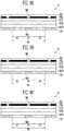
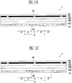
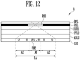
- FIGS. 9A to 12 are enlarged sectional views illustrating exemplary embodiments of area A of FIG 6 .
- FIGS. 9A to 12 illustrate different exemplary embodiments related to the resolutions, sizes, and/or arrangement relationships of the photo sensors PHS provided on the sensor layer 120.
- target areas TA corresponding to the respective pinholes PIH at least partially overlap with each other.
- the photo sensors PHS may be arranged at different resolutions between an area (hereinafter, referred to as a first area A1) in which target areas TA overlap with each other and an area (hereinafter, referred to as a second area A2) in which target areas TA do not overlap with each other.
- each first area A1 has been illustrated as having an area greater than that of each pinhole PIH, the inventive concept is not limited thereto. In other words, in some exemplary embodiments, each first area A1 may have an area equal to or less than that of each pinhole PIH. Some of these exemplary embodiments are illustrated in FIG 12 .
- photo sensors PHS are disposed at a first resolution in the first areas A1 on the sensor layer 120, and photo sensors PHS are disposed at a second resolution in the second areas A2 on the sensor layer 120.
- the first resolution is higher than the second resolution.
- the photo sensors PHS that are disposed in the second areas A2 are arranged at pitches greater than that of the photo sensors PHS disposed in the first areas A1, thus implementing a low resolution structure.
- a given photosensor in a second area A2 is a same first distance away from the photosensors PHS it is adjacent in the second area A2
- a given photosensor in a first area A1 is a same second distance away from the photosensors PHS it is adjacent in the first area A1, and the first distance is greater than the second distance.
- the photo sensors PHS that are disposed in the second area A2 may be arranged to be disposed collinearly with at least some of the photo sensors PHS that are disposed in the first areas A1, but the inventive concept is not limited thereto.
- the photo sensors PHS that are disposed in the second areas A2 may be aligned with spaces between the photo sensors PHS that are disposed in the first areas A1.
- each of the photo sensors PHS that are disposed in the second areas A2 has a width greater than that of each of the photo sensors PHS disposed in the first areas A1, thus implementing a low resolution structure.
- a photo diode of each of the photo sensors PHS disposed in the second areas A2 has an area greater than that of a photo diode of each of the photo sensors PHS disposed in the first areas A1.
- the inventive concept is not limited thereto.
- each of the photo sensors PHS disposed in the second areas A2 are manufactured to have a relatively large area in such a way that the circuit elements thereof are disposed at pitches greater than that of each of the photo sensors PHS disposed in the first areas A1.
- the photo sensors PHS are not disposed in the second areas A2.
- the target areas TA corresponding to the respective pinholes PIH come into contact with each other without overlapping with each other.
- the first areas A1 have sizes and shapes large enough to identify the fingerprint based on image data generated from sensing signals of the photo sensors PHS disposed in the first areas A1.
- the second areas A2 may be set to areas on the sensor layer 120 other than the first areas A1.
- the first areas A1 may at least partially overlap with the pinholes PIH.
- photo sensors PHS are disposed at a first resolution in the first areas A1 on the sensor layer 120, and photo sensors PHS are disposed at a second resolution in the second areas A2 on the sensor layer 120.
- the first resolution is higher than the second resolution.
- FIG 10 illustrates an example where the photo sensors PHS are disposed at a comparatively high resolution in the first areas A1 and at a comparatively low resolution in the second areas A2 and have the same area
- the inventive concept is not limited thereto.
- the photo sensors PHS that are disposed in the second areas A2 may have areas greater than that of the photo sensors PHS that are disposed in the first areas A1.
- the photo sensors PHS are not disposed in the second areas A2.
- target areas TA corresponding to the respective pinholes PIH are spaced apart from each other.
- the first areas A1 have sizes and shapes large enough to identify the fingerprint based on image data generated from sensing signals of the photo sensors PHS disposed in the first areas A1.
- the second areas A2 may be set to areas on the target areas TA other than the first areas A1.
- an area (hereinafter, referred to as a third area A3) between the target areas TA may have various shapes and sizes depending on the sizes and arrangements of the pinholes PIH, and the distance between the pinhole array layer PHL and the sensor layer 120.
- the photo sensors PHS corresponding to each of the pinholes PIH may have different resolutions between at least two areas of the first area A1, the second area A2, and the third area A3.
- the photo sensors PHS are disposed at a first resolution in the first areas A1 and at a second resolution in the second areas A2 and the third areas A3.
- the first resolution is higher than the second resolution.
- the photo sensors PHS that are disposed in the second areas A2 and the third areas A3 are arranged at pitches greater than that of the photo sensors PHS disposed in the first areas A1, thus implementing a low resolution structure.
- the photo sensors PHS that are disposed in the second area A2 and the third areas A3 may be arranged to be disposed collinearly with at least some of the photo sensors PHS disposed in the first areas A1, but the inventive concept is not limited thereto.
- the photo sensors PHS that are disposed in the second areas A2 and the third areas A3 may be aligned with spaces between the photo sensors PHS that are disposed in the first areas A1.
- each of the photo sensors PHS that are disposed in the second areas A2 and the third areas A3 is manufactured to have an area greater than that of each of the photo sensors PHS disposed in the first areas A1, thus implementing a low resolution structure.
- Detailed descriptions of this exemplary embodiment are the same as that described with reference to FIG 9B ; therefore, further explanation thereof will be omitted.
- the photo sensors PHS are disposed at a first resolution in the first areas A1, at a second resolution in the second areas A2, and at a third resolution in the third areas A3.
- the first resolution is higher than the second resolution
- the second resolution is higher than the third resolution.
- the photo sensors PHS that are disposed in the third areas A3 are disposed at pitches greater than that of the photo sensors PHS disposed in the second areas A2, thus implementing a low resolution structure.
- the photo sensors PHS that are disposed in the third area A3 may be arranged to be disposed collinearly with at least some of the photo sensors PHS that are disposed in the second areas A2, but the inventive concept is not limited thereto.
- the photo sensors PHS that are disposed in the third areas A3 may be aligned with spaces between the photo sensors PHS that are disposed in the second areas A2.
- the photo sensors PHS that are disposed in the third areas A3 may be aligned with at least some of the photo sensors PHS that are disposed in the first areas A1 or with spaces between the photo sensors PHS that are disposed in the first areas A1, depending on alignment between the photo sensors PHS that are disposed in the first areas A1 and the photo sensors PHS that are disposed in the second areas A2.
- each of the photo sensors PHS that are disposed in the third areas A3 are manufactured to have an area greater than that of each of the photo sensors PHS disposed in the second areas A2, thus implementing a low resolution structure.
- Detailed descriptions of this exemplary embodiment are the same as that described with reference to FIG 9B ; therefore, further explanation thereof will be omitted.
- the photo sensors PHS are not disposed in at least one of the second area A2 and the third area A3.
- FIG 11C illustrates an example where the photo sensors PHS are present in the second area A2 and not present in the third area A3, the inventive concept is not limited thereto.
- the photo sensors PHS are not present in the second area and present in the third area A3, and in yet another embodiment the photosensors PHS are not present in the second area A2 and not present in the third area A3.
- each first area A1 has a size (an area, a width, and a diameter) less than that of each pinhole PIH.
- each second area A2 may partially overlap with the pin hole PIH.
- the second area A2 may partially overlap with the pinhole PIH.
- the entirety of the second area A2 may overlap with the pinhole PIH.
- photo sensors PHS are disposed at a first resolution in the first areas A1 on the sensor layer 120, and photo sensors PHS are disposed at a second resolution in the second areas A2 on the sensor layer 120.
- the first resolution is higher than the second resolution.
- the inventive concept is not limited to that illustrated in FIG 12 .
- the photo sensors PHS may be arranged in various ways, as described with reference to FIGS. 9A to 11C . Detailed descriptions of these exemplary embodiments are the same as those described with reference to FIGS. 9A to 11C ; therefore, further explanation thereof will be omitted.
- the production cost of the sensor layer 120 may be reduced, and the production cost of the display device 10 may be consequently reduced.
- a method of arranging the photo sensors PHS is not limited to those described above.
- the arrangements and sizes of the photo sensors PHS relative to the pinholes PIH may be modified in various ways so long as the photo sensors PHS are arranged at different resolutions between different areas in the sensor layers 120.
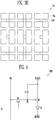
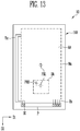
- FIG 13 is a plan view schematically illustrating a display device 10 in accordance with an exemplary embodiment of the inventive concept.
- the display device 10 of FIG 13 further includes a pad unit P, compared to that illustrated in FIG 1 .
- a plurality of electrodes IE which are electrically coupled with the photo sensors PHS may be formed in the pad unit P.
- some of the electrodes IE are coupled to horizontal sensing lines Tx, and some of the electrodes IE are coupled to vertical sensing lines Rx.
- some of the electrodes IE may be provided as dummy electrodes which are coupled neither to the horizontal sensing lines Tx nor to the vertical sensing lines Rx.
- the pad unit P may include the driving circuit 200 illustrated in FIGS. 1 and 2 or be coupled to the driving circuit 200.
- Driving signals output from the fingerprint detection unit 220 of the driving circuit 200 may be transmitted to the horizontal sensing lines Tx through the electrodes IE of the pad unit P.
- Sensing signals output through the vertical sensing lines Rx may be transmitted to the fingerprint detection unit 220 of the driving circuit 200 through the electrodes IE of the pad unit P.
- the horizontal sensing lines Tx are electrically coupled to a plurality of photo sensors PHS that are arranged in a horizontal direction (a first direction D1) on the display area AA.
- the horizontal sensing lines Tx may supply driving signals received from the electrodes IE to the photo sensors PHS coupled to the horizontal sensing lines Tx.
- the vertical sensing lines Rx are electrically coupled to a plurality of photo sensors PHS that are arranged in a vertical direction (a second direction D2) on the display area AA.
- the vertical sensing lines Rx may receive sensing signals output from the photo sensors PHS and transmit the received sensing signals to the electrodes IE.
- the photo sensors PHS may be disposed at intersections between the horizontal sensing lines Tx and the vertical sensing lines Rx.
- the photo sensors PHS may be configured to be turned on when driving signals are received from the horizontal sensing lines Tx, and configured to output sensing signals in response to the driving signals and the quantity of light that is incident on the photo sensors PHS.
- the number of photo sensors PHS that are electrically coupled to a first group of horizontal sensing lines Tx may be greater (or less) than that coupled to a second group of horizontal sensing lines Tx.
- the number of photo sensors PHS that are electrically coupled to a first group of vertical sensing lines Rx may be greater (or less) than that coupled to a second group of vertical sensing lines Rx.
- the inventive concept is not limited to those described above.
- the numbers of photo sensors PHS that are electrically coupled to the first and second groups of horizontal sensing lines Tx may be the same as each other, and the numbers of photo sensors PHS that are electrically coupled to the first and second groups of vertical sensing lines Rx may also be the same as each other.
- the first and second groups of horizontal sensing lines Tx may be spaced apart from each other, and the first and second groups of vertical sensing lines Rx may be spaced apart from each other.
- the inventive concept is not limited thereto.
- FIGS. 14A to 14D Exemplary embodiments related to connection relationships between the horizontal sensing lines Tx, the vertical sensing lines Rx, and the photo sensors PHS are illustrated in FIGS. 14A to 14D .
- the arrangement of the horizontal sensing lines Tx and the vertical sensing line Rx is not limited to that illustrated in FIG 13 .
- the terms “horizontal” and “vertical” used in this specification are only to distinguish relative arrangements thereof.
- the horizontal sensing lines Tx are not necessarily required to extend in the first direction D1 (e.g., a horizontal direction), and the vertical sensing lines Rx are also not necessarily required to extend in the second direction D2 (e.g., a vertical direction).
- the horizontal sensing lines Tx may extend in the second direction D2
- the vertical sensing lines Rx may extend in the first direction D1.
- FIGS. 14A to 14D are plan views illustrating a portion of the sensing area SA of FIG 13 according to an exemplary embodiment of the inventive concept. Particularly, FIGS. 14A to 14D illustrate exemplary embodiments related to connection relationships between the horizontal sensing lines Tx, the vertical sensing lines Rx, and the photo sensors PHS.
- the number of photo sensors PHS that are electrically coupled to a first group of horizontal sensing lines Tx may be greater (or less) than that coupled to a second group of horizontal sensing lines Tx.
- the number of photo sensors PHS that are electrically coupled to a first group of vertical sensing lines Rx may be greater (or less) than that coupled to a second group of vertical sensing lines Rx.
- the inventive concept is not limited to those described above.
- the numbers of photo sensors PHS that are electrically coupled to the first and second groups of horizontal sensing lines Tx may be the same as each other, and the numbers of photo sensors PHS that are electrically coupled to the first and second groups of vertical sensing lines Rx may also be the same as each other.
- the first and second groups of horizontal sensing lines Tx may be spaced apart from each other, and the first and second groups of vertical sensing lines Rx may be spaced apart from each other.
- m-th to m+5-th horizontal sensing lines Txm to Txm+5 and n-th to n+5-th vertical sensing lines Rxn to Rxn+5 are disposed in the sensing area SA.
- Photo sensors PHS are disposed at intersections between the horizontal sensing lines Tx and the vertical sensing lines Rx.
- the first group of horizontal sensing lines Tx includes the m+1-th to m+4-th horizontal sensing lines Txm+1 to Txm+4, and the second group of horizontal sensing lines Tx includes the m-th and m+5-th horizontal sensing lines Txm and Txm+5.
- the number of photo sensors PHS that is coupled to the first group of horizontal sensing lines Tx is greater than that coupled to the second group of horizontal sensing lines Tx.
- the first group of horizontal sensing lines Tx may at least partially overlap with the first areas A1 illustrated in FIGS. 9A to 12 .
- the second group of horizontal sensing lines Tx do not overlap with the first areas A1 illustrated in FIGS. 9A to 12 .
- the inventive concept is not limited thereto.
- the second group of horizontal sensing lines Tx may also at least partially overlap with the first areas A1 illustrated in FIGS. 9A to 12 .
- the area in which the first group of horizontal sensing lines Tx overlaps with the first areas A1 is greater than the area in which the second group overlaps with the first areas A1.
- the number of photo sensors PHS disposed in the first areas A1 on the sensor layer 120 is greater than that in the second areas A2. Therefore, the number of photo sensors PHS that are coupled to the first group of horizontal sensing lines Tx that overlaps with the first areas A1 is greater than that coupled to the second group of horizontal sensing lines Tx that does not overlap with the first areas A1 or is less in the overlapping area than the first group of horizontal sensing lines Tx.
- the first group of horizontal sensing lines Tx may extend in the horizontal direction without bending, as illustrated in FIG 14A .
- the first group of horizontal sensing lines Tx may be bent in at least an area, as illustrated in FIG 14B .
- the first group of horizontal sensing lines Tx may be bent in at least an area so as to couple the photo sensors PHS that are disposed in the first areas A1 and the second areas A2.
- Bent portions of the horizontal sensing lines Tx may be formed in boundaries between the first areas A1 and the second areas A2.
- the inventive concept is not limited thereto.
- the first group of horizontal sensing lines Tx may be formed in curved shapes in the boundaries between the first areas A1 and the second areas A2.
- the first group of horizontal sensing lines Tx may be bent or formed in curved shapes in other areas rather than the boundaries between the first areas A1 and the second areas A2.
- the first group of horizontal sensing lines Tx may be bent in at least an area such that the photo sensors PHS disposed in the first areas A1 do not overlap with the photo sensors PHS disposed in the second areas A2, as illustrated in FIG 14C .
- vertical sensing lines Rxn+1 and Rxn+4 each include a first bent portion when transitioning from a second area A2 to a first area A1, and a second bent portion when transitioning from the first area A1 to another second area A2
- horizontal sensing lines Txm+1 and Txm+4 each include a first bent portion when transitioning from a second area A2 to a first area A1, and a second bent portion when transitioning from the first area A1 to another second area A2.
- the numbers of photo sensors PHS that are coupled to the respective horizontal sensing lines Tx may be the same.
- at least some of the horizontal sensing lines Tx may be disposed to be spaced apart from each other in the second areas A2. The distance between the horizontal sensing lines Tx may be determined in various ways depending on whether the target areas TA overlap with each other, the sizes of the target areas TA, and the sizes of the first areas and the second areas.
- the first group of vertical sensing lines Rx includes the n+1-th to n+4-th vertical sensing lines Rxn+1 to Rxn+4, and the second group thereof includes the n-th and n+5-th vertical sensing lines Rxn and Rxn+5.
- the number of photo sensors PHS that is coupled to the first group of vertical sensing lines Rx is greater than that coupled to the second group.
- the first group of vertical sensing lines Rx may at least partially overlap with the first areas A1 illustrated in FIGS. 9A to 12 .
- the second group of vertical sensing lines Rx does not overlap with the first areas A1 illustrated in FIGS. 9A to 12 .
- the inventive concept is not limited thereto.
- the second group of vertical sensing lines Rx may also at least partially overlap with the first areas A1 illustrated in FIGS. 9A to 12 .
- the area in which the first group of vertical sensing lines Rx overlaps with the first areas A1 is greater than the area in which the second group overlaps with the first areas A1.
- the number of photo sensors PHS that are coupled to the first group of vertical sensing lines Rx is greater than that coupled to the second group.
- the connection relationship between the vertical sensing lines Rx and the photo sensors PHS is the same as that described for the horizontal sensing lines Tx with reference to FIGS. 14A to 14D ; therefore, further explanation thereof will be omitted.
- FIGS. 14A to 14D illustrate exemplary embodiments in which the horizontal sensing lines Tx and the vertical sensing lines Rx are arranged in the same shape
- the inventive concept is not limited thereto.
- the arrangement shape of the horizontal sensing lines Tx and the vertical sensing lines Rx may be modified in various ways depending on the array state of the photo sensors PHS.
- the horizontal sensing lines Tx and/or the vertical sensing lines Rx may be disposed in an area in the same manner as that illustrated in FIG 14A and disposed in the other area in the same manner as that illustrated in FIG 14B .
- the horizontal sensing lines Tx and/or the vertical sensing lines Rx may be disposed in an area in the same manner as that illustrated in FIG 14A or 14B and disposed in the other area in the same manner as that illustrated in FIG 14C .
- high resolution photo sensors are arranged in only some areas in a sensor layer, and low resolution photo sensors may be arranged in the other areas or no photo sensor may be provided therein. Therefore, the production cost of the display device may be reduced.
Landscapes
- Engineering & Computer Science (AREA)
- Theoretical Computer Science (AREA)
- General Physics & Mathematics (AREA)
- Physics & Mathematics (AREA)
- Multimedia (AREA)
- Human Computer Interaction (AREA)
- Vascular Medicine (AREA)
- Health & Medical Sciences (AREA)
- General Health & Medical Sciences (AREA)
- Life Sciences & Earth Sciences (AREA)
- Chemical & Material Sciences (AREA)
- Inorganic Chemistry (AREA)
- Sustainable Development (AREA)
- Image Input (AREA)
- Devices For Indicating Variable Information By Combining Individual Elements (AREA)
Applications Claiming Priority (1)
| Application Number | Priority Date | Filing Date | Title |
|---|---|---|---|
| KR1020190001340A KR102808360B1 (ko) | 2019-01-04 | 2019-01-04 | 지문 센서 및 이를 포함하는 표시 장치 |
Publications (2)
| Publication Number | Publication Date |
|---|---|
| EP3678052A1 true EP3678052A1 (de) | 2020-07-08 |
| EP3678052B1 EP3678052B1 (de) | 2024-02-28 |
Family
ID=69137710
Family Applications (1)
| Application Number | Title | Priority Date | Filing Date |
|---|---|---|---|
| EP20150196.2A Active EP3678052B1 (de) | 2019-01-04 | 2020-01-03 | Fingerabdrucksensor und anzeigevorrichtung damit |
Country Status (4)
| Country | Link |
|---|---|
| US (2) | US11521995B2 (de) |
| EP (1) | EP3678052B1 (de) |
| KR (1) | KR102808360B1 (de) |
| CN (1) | CN111414795B (de) |
Families Citing this family (13)
| Publication number | Priority date | Publication date | Assignee | Title |
|---|---|---|---|---|
| JP7240151B2 (ja) * | 2018-11-22 | 2023-03-15 | 株式会社ジャパンディスプレイ | 検出装置及び表示装置 |
| KR102808360B1 (ko) * | 2019-01-04 | 2025-05-19 | 삼성디스플레이 주식회사 | 지문 센서 및 이를 포함하는 표시 장치 |
| CN109784303B (zh) * | 2019-01-29 | 2021-07-30 | 上海天马微电子有限公司 | 显示装置 |
| KR102743357B1 (ko) | 2019-04-24 | 2024-12-18 | 삼성디스플레이 주식회사 | 표시 장치 |
| KR102872943B1 (ko) | 2019-06-11 | 2025-10-20 | 삼성디스플레이 주식회사 | 표시 장치 |
| US11832473B2 (en) | 2019-06-26 | 2023-11-28 | Oti Lumionics Inc. | Optoelectronic device including light transmissive regions, with light diffraction characteristics |
| CN114097102B (zh) | 2019-06-26 | 2023-11-03 | Oti照明公司 | 包括具有光衍射特征的光透射区域的光电设备 |
| CN114342068A (zh) | 2019-08-09 | 2022-04-12 | Oti照明公司 | 包含辅助电极和分区的光电子装置 |
| WO2022123431A1 (en) | 2020-12-07 | 2022-06-16 | Oti Lumionics Inc. | Patterning a conductive deposited layer using a nucleation inhibiting coating and an underlying metallic coating |
| KR102810624B1 (ko) * | 2021-02-23 | 2025-05-22 | 삼성디스플레이 주식회사 | 픽셀 회로, 이를 포함하는 표시 장치 및 이의 구동 방법 |
| JP7823863B2 (ja) * | 2021-05-20 | 2026-03-04 | 株式会社Magnolia White | 光学素子及び電子機器 |
| CN114284319B (zh) * | 2021-12-14 | 2023-09-26 | 武汉华星光电半导体显示技术有限公司 | 显示面板及电子设备 |
| CN119789704A (zh) * | 2024-11-15 | 2025-04-08 | 厦门天马显示科技有限公司 | 显示面板及显示装置 |
Citations (3)
| Publication number | Priority date | Publication date | Assignee | Title |
|---|---|---|---|---|
| US20170017824A1 (en) * | 2015-02-02 | 2017-01-19 | Synaptics Incorporated | Low profile illumination in an optical fingerprint sensor |
| WO2017211152A1 (en) * | 2016-06-07 | 2017-12-14 | Shenzhen GOODIX Technology Co., Ltd. | Optical collimators for under-screen optical sensor module for on-screen fingerprint sensing |
| EP3267359A1 (de) * | 2016-07-06 | 2018-01-10 | Samsung Electronics Co., Ltd | Fingerabdrucksensor, fingerabdrucksensorsystem und sensorsystem das die lichtquellen des bildschirms benutzt |
Family Cites Families (17)
| Publication number | Priority date | Publication date | Assignee | Title |
|---|---|---|---|---|
| US10147757B2 (en) * | 2015-02-02 | 2018-12-04 | Synaptics Incorporated | Image sensor structures for fingerprint sensing |
| JPWO2016148186A1 (ja) | 2015-03-16 | 2017-04-27 | 積水化学工業株式会社 | 太陽電池 |
| CN107430681B (zh) | 2015-03-25 | 2021-02-09 | 苹果公司 | 包括光学图像传感器上方的针孔阵列掩膜的电子设备及相关方法 |
| EP3278272B1 (de) * | 2015-06-18 | 2020-12-09 | Shenzhen Goodix Technology Co., Ltd. | Multifunktionsfingerabdrucksensor mit optischer abtastfähigkeit |
| US9721142B2 (en) * | 2015-06-26 | 2017-08-01 | Synaptics Incorporated | Multi-resolution fingerprint sensor |
| US9524416B1 (en) * | 2015-07-03 | 2016-12-20 | Fingerprint Cards Ab | Fingerprint sensing device comprising three-dimensional pattern |
| US10387711B2 (en) * | 2016-03-07 | 2019-08-20 | Microsoft Technology Licensing, Llc | Pixel having a photoemitter and a photodetector triggered by a pixel selector signal bus |
| KR20180005588A (ko) | 2016-07-06 | 2018-01-16 | 삼성전자주식회사 | 디스플레이 패널의 광원들을 이용한 지문 센서, 지문 센서 패키지 및 지문 센싱 시스템 |
| JP6691110B2 (ja) | 2016-08-25 | 2020-04-28 | 北京小米移動軟件有限公司Beijing Xiaomi Mobile Software Co.,Ltd. | 表示パネル、端末及び表示制御方法 |
| KR102635898B1 (ko) * | 2016-10-25 | 2024-02-15 | 엘지디스플레이 주식회사 | 지문센서 일체형 터치 스크린 장치 |
| KR102838254B1 (ko) | 2017-02-22 | 2025-07-28 | 삼성디스플레이 주식회사 | 지문 센서 및 이의 제조 방법 |
| KR102295068B1 (ko) * | 2017-03-31 | 2021-08-31 | 삼성디스플레이 주식회사 | 표시 장치 및 그의 구동 방법 |
| CN107168465B (zh) * | 2017-05-15 | 2020-01-31 | 京东方科技集团股份有限公司 | 显示模组及显示装置 |
| US10809853B2 (en) * | 2017-12-11 | 2020-10-20 | Will Semiconductor (Shanghai) Co. Ltd. | Optical sensor having apertures |
| US10755070B2 (en) * | 2017-12-12 | 2020-08-25 | Silicon Display Technology | Sensor pixel, fingerprint and image sensor including the same, and driving method thereof |
| KR102643092B1 (ko) | 2018-10-02 | 2024-03-06 | 삼성디스플레이 주식회사 | 지문 센서 및 이를 구비한 표시 장치 |
| KR102808360B1 (ko) | 2019-01-04 | 2025-05-19 | 삼성디스플레이 주식회사 | 지문 센서 및 이를 포함하는 표시 장치 |
-
2019
- 2019-01-04 KR KR1020190001340A patent/KR102808360B1/ko active Active
- 2019-11-22 US US16/692,239 patent/US11521995B2/en active Active
-
2020
- 2020-01-03 EP EP20150196.2A patent/EP3678052B1/de active Active
- 2020-01-03 CN CN202010004543.6A patent/CN111414795B/zh active Active
-
2022
- 2022-12-05 US US18/061,520 patent/US11830282B2/en active Active
Patent Citations (3)
| Publication number | Priority date | Publication date | Assignee | Title |
|---|---|---|---|---|
| US20170017824A1 (en) * | 2015-02-02 | 2017-01-19 | Synaptics Incorporated | Low profile illumination in an optical fingerprint sensor |
| WO2017211152A1 (en) * | 2016-06-07 | 2017-12-14 | Shenzhen GOODIX Technology Co., Ltd. | Optical collimators for under-screen optical sensor module for on-screen fingerprint sensing |
| EP3267359A1 (de) * | 2016-07-06 | 2018-01-10 | Samsung Electronics Co., Ltd | Fingerabdrucksensor, fingerabdrucksensorsystem und sensorsystem das die lichtquellen des bildschirms benutzt |
Also Published As
| Publication number | Publication date |
|---|---|
| US20230094986A1 (en) | 2023-03-30 |
| CN111414795A (zh) | 2020-07-14 |
| CN111414795B (zh) | 2025-08-12 |
| US11521995B2 (en) | 2022-12-06 |
| KR20200085401A (ko) | 2020-07-15 |
| EP3678052B1 (de) | 2024-02-28 |
| US20200219915A1 (en) | 2020-07-09 |
| US11830282B2 (en) | 2023-11-28 |
| KR102808360B1 (ko) | 2025-05-19 |
Similar Documents
| Publication | Publication Date | Title |
|---|---|---|
| US11830282B2 (en) | Fingerprint sensor and display device including the same | |
| US11024682B2 (en) | Fingerprint sensor and display device including the same | |
| KR102743357B1 (ko) | 표시 장치 | |
| US12238982B2 (en) | Display device including light-blocking layer and sensor layer | |
| KR102643092B1 (ko) | 지문 센서 및 이를 구비한 표시 장치 | |
| US11825669B2 (en) | Electroluminescent device | |
| KR102400868B1 (ko) | 표시 장치 | |
| KR102632590B1 (ko) | 터치 센서 및 이를 포함한 표시 장치 | |
| CN108604296B (zh) | 发光指纹识别面板及包括其的指纹识别显示装置 | |
| US11200398B2 (en) | Display device and method of driving display device | |
| KR20200142641A (ko) | 표시 장치 | |
| KR102778739B1 (ko) | 표시 장치 및 휴대용 단말기 | |
| KR20190048985A (ko) | 터치센서를 포함하는 표시장치 및 그의 제조방법 | |
| KR20200137081A (ko) | 지문 센서 및 이를 포함하는 표시 장치 | |
| CN116390596A (zh) | 显示面板和显示装置 | |
| US11295106B2 (en) | Display device and driving method thereof | |
| US12229359B2 (en) | Display device and driving method with variable frequency of display according to fingerprint sensing | |
| US10769988B2 (en) | Display device configured to measure light and adjust display brightness and a method of driving the same | |
| KR20240050556A (ko) | 표시장치 | |
| KR20250019945A (ko) | 터치 디스플레이 장치 |
Legal Events
| Date | Code | Title | Description |
|---|---|---|---|
| PUAI | Public reference made under article 153(3) epc to a published international application that has entered the european phase |
Free format text: ORIGINAL CODE: 0009012 |
|
| STAA | Information on the status of an ep patent application or granted ep patent |
Free format text: STATUS: THE APPLICATION HAS BEEN PUBLISHED |
|
| AK | Designated contracting states |
Kind code of ref document: A1 Designated state(s): AL AT BE BG CH CY CZ DE DK EE ES FI FR GB GR HR HU IE IS IT LI LT LU LV MC MK MT NL NO PL PT RO RS SE SI SK SM TR |
|
| AX | Request for extension of the european patent |
Extension state: BA ME |
|
| STAA | Information on the status of an ep patent application or granted ep patent |
Free format text: STATUS: REQUEST FOR EXAMINATION WAS MADE |
|
| 17P | Request for examination filed |
Effective date: 20210108 |
|
| RBV | Designated contracting states (corrected) |
Designated state(s): AL AT BE BG CH CY CZ DE DK EE ES FI FR GB GR HR HU IE IS IT LI LT LU LV MC MK MT NL NO PL PT RO RS SE SI SK SM TR |
|
| STAA | Information on the status of an ep patent application or granted ep patent |
Free format text: STATUS: EXAMINATION IS IN PROGRESS |
|
| 17Q | First examination report despatched |
Effective date: 20220228 |
|
| P01 | Opt-out of the competence of the unified patent court (upc) registered |
Effective date: 20230516 |
|
| REG | Reference to a national code |
Ref legal event code: R079 Ipc: G06V0040130000 Ref country code: DE Ref legal event code: R079 Ref document number: 602020026265 Country of ref document: DE Free format text: PREVIOUS MAIN CLASS: G06K0009000000 Ipc: G06V0040130000 |
|
| GRAP | Despatch of communication of intention to grant a patent |
Free format text: ORIGINAL CODE: EPIDOSNIGR1 |
|
| STAA | Information on the status of an ep patent application or granted ep patent |
Free format text: STATUS: GRANT OF PATENT IS INTENDED |
|
| RIC1 | Information provided on ipc code assigned before grant |
Ipc: G06V 40/13 20220101AFI20230814BHEP |
|
| INTG | Intention to grant announced |
Effective date: 20230913 |
|
| GRAS | Grant fee paid |
Free format text: ORIGINAL CODE: EPIDOSNIGR3 |
|
| GRAA | (expected) grant |
Free format text: ORIGINAL CODE: 0009210 |
|
| STAA | Information on the status of an ep patent application or granted ep patent |
Free format text: STATUS: THE PATENT HAS BEEN GRANTED |
|
| AK | Designated contracting states |
Kind code of ref document: B1 Designated state(s): AL AT BE BG CH CY CZ DE DK EE ES FI FR GB GR HR HU IE IS IT LI LT LU LV MC MK MT NL NO PL PT RO RS SE SI SK SM TR |
|
| REG | Reference to a national code |
Ref country code: GB Ref legal event code: FG4D |
|
| REG | Reference to a national code |
Ref country code: CH Ref legal event code: EP |
|
| REG | Reference to a national code |
Ref country code: DE Ref legal event code: R096 Ref document number: 602020026265 Country of ref document: DE |
|
| REG | Reference to a national code |
Ref country code: IE Ref legal event code: FG4D |
|
| REG | Reference to a national code |
Ref country code: LT Ref legal event code: MG9D |
|
| PG25 | Lapsed in a contracting state [announced via postgrant information from national office to epo] |
Ref country code: IS Free format text: LAPSE BECAUSE OF FAILURE TO SUBMIT A TRANSLATION OF THE DESCRIPTION OR TO PAY THE FEE WITHIN THE PRESCRIBED TIME-LIMIT Effective date: 20240628 |
|
| REG | Reference to a national code |
Ref country code: NL Ref legal event code: MP Effective date: 20240228 |
|
| PG25 | Lapsed in a contracting state [announced via postgrant information from national office to epo] |
Ref country code: LT Free format text: LAPSE BECAUSE OF FAILURE TO SUBMIT A TRANSLATION OF THE DESCRIPTION OR TO PAY THE FEE WITHIN THE PRESCRIBED TIME-LIMIT Effective date: 20240228 |
|
| PG25 | Lapsed in a contracting state [announced via postgrant information from national office to epo] |
Ref country code: GR Free format text: LAPSE BECAUSE OF FAILURE TO SUBMIT A TRANSLATION OF THE DESCRIPTION OR TO PAY THE FEE WITHIN THE PRESCRIBED TIME-LIMIT Effective date: 20240529 |
|
| PG25 | Lapsed in a contracting state [announced via postgrant information from national office to epo] |
Ref country code: RS Free format text: LAPSE BECAUSE OF FAILURE TO SUBMIT A TRANSLATION OF THE DESCRIPTION OR TO PAY THE FEE WITHIN THE PRESCRIBED TIME-LIMIT Effective date: 20240528 Ref country code: HR Free format text: LAPSE BECAUSE OF FAILURE TO SUBMIT A TRANSLATION OF THE DESCRIPTION OR TO PAY THE FEE WITHIN THE PRESCRIBED TIME-LIMIT Effective date: 20240228 Ref country code: NL Free format text: LAPSE BECAUSE OF FAILURE TO SUBMIT A TRANSLATION OF THE DESCRIPTION OR TO PAY THE FEE WITHIN THE PRESCRIBED TIME-LIMIT Effective date: 20240228 |
|
| PG25 | Lapsed in a contracting state [announced via postgrant information from national office to epo] |
Ref country code: ES Free format text: LAPSE BECAUSE OF FAILURE TO SUBMIT A TRANSLATION OF THE DESCRIPTION OR TO PAY THE FEE WITHIN THE PRESCRIBED TIME-LIMIT Effective date: 20240228 |
|
| PG25 | Lapsed in a contracting state [announced via postgrant information from national office to epo] |
Ref country code: RS Free format text: LAPSE BECAUSE OF FAILURE TO SUBMIT A TRANSLATION OF THE DESCRIPTION OR TO PAY THE FEE WITHIN THE PRESCRIBED TIME-LIMIT Effective date: 20240528 Ref country code: NO Free format text: LAPSE BECAUSE OF FAILURE TO SUBMIT A TRANSLATION OF THE DESCRIPTION OR TO PAY THE FEE WITHIN THE PRESCRIBED TIME-LIMIT Effective date: 20240528 Ref country code: NL Free format text: LAPSE BECAUSE OF FAILURE TO SUBMIT A TRANSLATION OF THE DESCRIPTION OR TO PAY THE FEE WITHIN THE PRESCRIBED TIME-LIMIT Effective date: 20240228 Ref country code: LT Free format text: LAPSE BECAUSE OF FAILURE TO SUBMIT A TRANSLATION OF THE DESCRIPTION OR TO PAY THE FEE WITHIN THE PRESCRIBED TIME-LIMIT Effective date: 20240228 Ref country code: IS Free format text: LAPSE BECAUSE OF FAILURE TO SUBMIT A TRANSLATION OF THE DESCRIPTION OR TO PAY THE FEE WITHIN THE PRESCRIBED TIME-LIMIT Effective date: 20240628 Ref country code: HR Free format text: LAPSE BECAUSE OF FAILURE TO SUBMIT A TRANSLATION OF THE DESCRIPTION OR TO PAY THE FEE WITHIN THE PRESCRIBED TIME-LIMIT Effective date: 20240228 Ref country code: GR Free format text: LAPSE BECAUSE OF FAILURE TO SUBMIT A TRANSLATION OF THE DESCRIPTION OR TO PAY THE FEE WITHIN THE PRESCRIBED TIME-LIMIT Effective date: 20240529 Ref country code: FI Free format text: LAPSE BECAUSE OF FAILURE TO SUBMIT A TRANSLATION OF THE DESCRIPTION OR TO PAY THE FEE WITHIN THE PRESCRIBED TIME-LIMIT Effective date: 20240228 Ref country code: ES Free format text: LAPSE BECAUSE OF FAILURE TO SUBMIT A TRANSLATION OF THE DESCRIPTION OR TO PAY THE FEE WITHIN THE PRESCRIBED TIME-LIMIT Effective date: 20240228 Ref country code: BG Free format text: LAPSE BECAUSE OF FAILURE TO SUBMIT A TRANSLATION OF THE DESCRIPTION OR TO PAY THE FEE WITHIN THE PRESCRIBED TIME-LIMIT Effective date: 20240228 |
|
| PG25 | Lapsed in a contracting state [announced via postgrant information from national office to epo] |
Ref country code: PL Free format text: LAPSE BECAUSE OF FAILURE TO SUBMIT A TRANSLATION OF THE DESCRIPTION OR TO PAY THE FEE WITHIN THE PRESCRIBED TIME-LIMIT Effective date: 20240228 Ref country code: PT Free format text: LAPSE BECAUSE OF FAILURE TO SUBMIT A TRANSLATION OF THE DESCRIPTION OR TO PAY THE FEE WITHIN THE PRESCRIBED TIME-LIMIT Effective date: 20240628 |
|
| REG | Reference to a national code |
Ref country code: AT Ref legal event code: MK05 Ref document number: 1661952 Country of ref document: AT Kind code of ref document: T Effective date: 20240228 |
|
| PG25 | Lapsed in a contracting state [announced via postgrant information from national office to epo] |
Ref country code: SE Free format text: LAPSE BECAUSE OF FAILURE TO SUBMIT A TRANSLATION OF THE DESCRIPTION OR TO PAY THE FEE WITHIN THE PRESCRIBED TIME-LIMIT Effective date: 20240228 Ref country code: PT Free format text: LAPSE BECAUSE OF FAILURE TO SUBMIT A TRANSLATION OF THE DESCRIPTION OR TO PAY THE FEE WITHIN THE PRESCRIBED TIME-LIMIT Effective date: 20240628 Ref country code: PL Free format text: LAPSE BECAUSE OF FAILURE TO SUBMIT A TRANSLATION OF THE DESCRIPTION OR TO PAY THE FEE WITHIN THE PRESCRIBED TIME-LIMIT Effective date: 20240228 Ref country code: LV Free format text: LAPSE BECAUSE OF FAILURE TO SUBMIT A TRANSLATION OF THE DESCRIPTION OR TO PAY THE FEE WITHIN THE PRESCRIBED TIME-LIMIT Effective date: 20240228 |
|
| PG25 | Lapsed in a contracting state [announced via postgrant information from national office to epo] |
Ref country code: DK Free format text: LAPSE BECAUSE OF FAILURE TO SUBMIT A TRANSLATION OF THE DESCRIPTION OR TO PAY THE FEE WITHIN THE PRESCRIBED TIME-LIMIT Effective date: 20240228 |
|
| PG25 | Lapsed in a contracting state [announced via postgrant information from national office to epo] |
Ref country code: SM Free format text: LAPSE BECAUSE OF FAILURE TO SUBMIT A TRANSLATION OF THE DESCRIPTION OR TO PAY THE FEE WITHIN THE PRESCRIBED TIME-LIMIT Effective date: 20240228 |
|
| PG25 | Lapsed in a contracting state [announced via postgrant information from national office to epo] |
Ref country code: CZ Free format text: LAPSE BECAUSE OF FAILURE TO SUBMIT A TRANSLATION OF THE DESCRIPTION OR TO PAY THE FEE WITHIN THE PRESCRIBED TIME-LIMIT Effective date: 20240228 Ref country code: EE Free format text: LAPSE BECAUSE OF FAILURE TO SUBMIT A TRANSLATION OF THE DESCRIPTION OR TO PAY THE FEE WITHIN THE PRESCRIBED TIME-LIMIT Effective date: 20240228 |
|
| PG25 | Lapsed in a contracting state [announced via postgrant information from national office to epo] |
Ref country code: AT Free format text: LAPSE BECAUSE OF FAILURE TO SUBMIT A TRANSLATION OF THE DESCRIPTION OR TO PAY THE FEE WITHIN THE PRESCRIBED TIME-LIMIT Effective date: 20240228 |
|
| PG25 | Lapsed in a contracting state [announced via postgrant information from national office to epo] |
Ref country code: SK Free format text: LAPSE BECAUSE OF FAILURE TO SUBMIT A TRANSLATION OF THE DESCRIPTION OR TO PAY THE FEE WITHIN THE PRESCRIBED TIME-LIMIT Effective date: 20240228 |
|
| PG25 | Lapsed in a contracting state [announced via postgrant information from national office to epo] |
Ref country code: SM Free format text: LAPSE BECAUSE OF FAILURE TO SUBMIT A TRANSLATION OF THE DESCRIPTION OR TO PAY THE FEE WITHIN THE PRESCRIBED TIME-LIMIT Effective date: 20240228 Ref country code: SK Free format text: LAPSE BECAUSE OF FAILURE TO SUBMIT A TRANSLATION OF THE DESCRIPTION OR TO PAY THE FEE WITHIN THE PRESCRIBED TIME-LIMIT Effective date: 20240228 Ref country code: RO Free format text: LAPSE BECAUSE OF FAILURE TO SUBMIT A TRANSLATION OF THE DESCRIPTION OR TO PAY THE FEE WITHIN THE PRESCRIBED TIME-LIMIT Effective date: 20240228 Ref country code: EE Free format text: LAPSE BECAUSE OF FAILURE TO SUBMIT A TRANSLATION OF THE DESCRIPTION OR TO PAY THE FEE WITHIN THE PRESCRIBED TIME-LIMIT Effective date: 20240228 Ref country code: DK Free format text: LAPSE BECAUSE OF FAILURE TO SUBMIT A TRANSLATION OF THE DESCRIPTION OR TO PAY THE FEE WITHIN THE PRESCRIBED TIME-LIMIT Effective date: 20240228 Ref country code: CZ Free format text: LAPSE BECAUSE OF FAILURE TO SUBMIT A TRANSLATION OF THE DESCRIPTION OR TO PAY THE FEE WITHIN THE PRESCRIBED TIME-LIMIT Effective date: 20240228 Ref country code: AT Free format text: LAPSE BECAUSE OF FAILURE TO SUBMIT A TRANSLATION OF THE DESCRIPTION OR TO PAY THE FEE WITHIN THE PRESCRIBED TIME-LIMIT Effective date: 20240228 |
|
| REG | Reference to a national code |
Ref country code: DE Ref legal event code: R097 Ref document number: 602020026265 Country of ref document: DE |
|
| PG25 | Lapsed in a contracting state [announced via postgrant information from national office to epo] |
Ref country code: IT Free format text: LAPSE BECAUSE OF FAILURE TO SUBMIT A TRANSLATION OF THE DESCRIPTION OR TO PAY THE FEE WITHIN THE PRESCRIBED TIME-LIMIT Effective date: 20240228 |
|
| PG25 | Lapsed in a contracting state [announced via postgrant information from national office to epo] |
Ref country code: IT Free format text: LAPSE BECAUSE OF FAILURE TO SUBMIT A TRANSLATION OF THE DESCRIPTION OR TO PAY THE FEE WITHIN THE PRESCRIBED TIME-LIMIT Effective date: 20240228 |
|
| PLBE | No opposition filed within time limit |
Free format text: ORIGINAL CODE: 0009261 |
|
| STAA | Information on the status of an ep patent application or granted ep patent |
Free format text: STATUS: NO OPPOSITION FILED WITHIN TIME LIMIT |
|
| PGFP | Annual fee paid to national office [announced via postgrant information from national office to epo] |
Ref country code: GB Payment date: 20241223 Year of fee payment: 6 |
|
| PGFP | Annual fee paid to national office [announced via postgrant information from national office to epo] |
Ref country code: FR Payment date: 20241224 Year of fee payment: 6 |
|
| 26N | No opposition filed |
Effective date: 20241129 |
|
| PGFP | Annual fee paid to national office [announced via postgrant information from national office to epo] |
Ref country code: DE Payment date: 20241223 Year of fee payment: 6 |
|
| PG25 | Lapsed in a contracting state [announced via postgrant information from national office to epo] |
Ref country code: SI Free format text: LAPSE BECAUSE OF FAILURE TO SUBMIT A TRANSLATION OF THE DESCRIPTION OR TO PAY THE FEE WITHIN THE PRESCRIBED TIME-LIMIT Effective date: 20240228 |
|
| REG | Reference to a national code |
Ref country code: CH Ref legal event code: PL |
|
| PG25 | Lapsed in a contracting state [announced via postgrant information from national office to epo] |
Ref country code: MC Free format text: LAPSE BECAUSE OF FAILURE TO SUBMIT A TRANSLATION OF THE DESCRIPTION OR TO PAY THE FEE WITHIN THE PRESCRIBED TIME-LIMIT Effective date: 20240228 Ref country code: LU Free format text: LAPSE BECAUSE OF NON-PAYMENT OF DUE FEES Effective date: 20250103 |
|
| PG25 | Lapsed in a contracting state [announced via postgrant information from national office to epo] |
Ref country code: BE Free format text: LAPSE BECAUSE OF NON-PAYMENT OF DUE FEES Effective date: 20250131 |
|
| PG25 | Lapsed in a contracting state [announced via postgrant information from national office to epo] |
Ref country code: CH Free format text: LAPSE BECAUSE OF NON-PAYMENT OF DUE FEES Effective date: 20250131 |
|
| REG | Reference to a national code |
Ref country code: BE Ref legal event code: MM Effective date: 20250131 |
|
| PG25 | Lapsed in a contracting state [announced via postgrant information from national office to epo] |
Ref country code: IE Free format text: LAPSE BECAUSE OF NON-PAYMENT OF DUE FEES Effective date: 20250103 |