EP3677966A1 - Exposure device, exposure method, and photolithography method - Google Patents
Exposure device, exposure method, and photolithography method Download PDFInfo
- Publication number
- EP3677966A1 EP3677966A1 EP18772701.1A EP18772701A EP3677966A1 EP 3677966 A1 EP3677966 A1 EP 3677966A1 EP 18772701 A EP18772701 A EP 18772701A EP 3677966 A1 EP3677966 A1 EP 3677966A1
- Authority
- EP
- European Patent Office
- Prior art keywords
- light valve
- exposure
- light
- valve array
- reflectivity
- Prior art date
- Legal status (The legal status is an assumption and is not a legal conclusion. Google has not performed a legal analysis and makes no representation as to the accuracy of the status listed.)
- Withdrawn
Links
Images




Classifications
-
- G—PHYSICS
- G03—PHOTOGRAPHY; CINEMATOGRAPHY; ANALOGOUS TECHNIQUES USING WAVES OTHER THAN OPTICAL WAVES; ELECTROGRAPHY; HOLOGRAPHY
- G03F—PHOTOMECHANICAL PRODUCTION OF TEXTURED OR PATTERNED SURFACES, e.g. FOR PRINTING, FOR PROCESSING OF SEMICONDUCTOR DEVICES; MATERIALS THEREFOR; ORIGINALS THEREFOR; APPARATUS SPECIALLY ADAPTED THEREFOR
- G03F7/00—Photomechanical, e.g. photolithographic, production of textured or patterned surfaces, e.g. printing surfaces; Materials therefor, e.g. comprising photoresists; Apparatus specially adapted therefor
- G03F7/20—Exposure; Apparatus therefor
- G03F7/2002—Exposure; Apparatus therefor with visible light or UV light, through an original having an opaque pattern on a transparent support, e.g. film printing, projection printing; by reflection of visible or UV light from an original such as a printed image
-
- G—PHYSICS
- G03—PHOTOGRAPHY; CINEMATOGRAPHY; ANALOGOUS TECHNIQUES USING WAVES OTHER THAN OPTICAL WAVES; ELECTROGRAPHY; HOLOGRAPHY
- G03F—PHOTOMECHANICAL PRODUCTION OF TEXTURED OR PATTERNED SURFACES, e.g. FOR PRINTING, FOR PROCESSING OF SEMICONDUCTOR DEVICES; MATERIALS THEREFOR; ORIGINALS THEREFOR; APPARATUS SPECIALLY ADAPTED THEREFOR
- G03F7/00—Photomechanical, e.g. photolithographic, production of textured or patterned surfaces, e.g. printing surfaces; Materials therefor, e.g. comprising photoresists; Apparatus specially adapted therefor
- G03F7/70—Microphotolithographic exposure; Apparatus therefor
- G03F7/70058—Mask illumination systems
- G03F7/70075—Homogenization of illumination intensity in the mask plane by using an integrator, e.g. fly's eye lens, facet mirror or glass rod, by using a diffusing optical element or by beam deflection
-
- G—PHYSICS
- G03—PHOTOGRAPHY; CINEMATOGRAPHY; ANALOGOUS TECHNIQUES USING WAVES OTHER THAN OPTICAL WAVES; ELECTROGRAPHY; HOLOGRAPHY
- G03F—PHOTOMECHANICAL PRODUCTION OF TEXTURED OR PATTERNED SURFACES, e.g. FOR PRINTING, FOR PROCESSING OF SEMICONDUCTOR DEVICES; MATERIALS THEREFOR; ORIGINALS THEREFOR; APPARATUS SPECIALLY ADAPTED THEREFOR
- G03F7/00—Photomechanical, e.g. photolithographic, production of textured or patterned surfaces, e.g. printing surfaces; Materials therefor, e.g. comprising photoresists; Apparatus specially adapted therefor
- G03F7/70—Microphotolithographic exposure; Apparatus therefor
- G03F7/70058—Mask illumination systems
- G03F7/7015—Details of optical elements
-
- G—PHYSICS
- G03—PHOTOGRAPHY; CINEMATOGRAPHY; ANALOGOUS TECHNIQUES USING WAVES OTHER THAN OPTICAL WAVES; ELECTROGRAPHY; HOLOGRAPHY
- G03F—PHOTOMECHANICAL PRODUCTION OF TEXTURED OR PATTERNED SURFACES, e.g. FOR PRINTING, FOR PROCESSING OF SEMICONDUCTOR DEVICES; MATERIALS THEREFOR; ORIGINALS THEREFOR; APPARATUS SPECIALLY ADAPTED THEREFOR
- G03F7/00—Photomechanical, e.g. photolithographic, production of textured or patterned surfaces, e.g. printing surfaces; Materials therefor, e.g. comprising photoresists; Apparatus specially adapted therefor
- G03F7/20—Exposure; Apparatus therefor
- G03F7/2002—Exposure; Apparatus therefor with visible light or UV light, through an original having an opaque pattern on a transparent support, e.g. film printing, projection printing; by reflection of visible or UV light from an original such as a printed image
- G03F7/2008—Exposure; Apparatus therefor with visible light or UV light, through an original having an opaque pattern on a transparent support, e.g. film printing, projection printing; by reflection of visible or UV light from an original such as a printed image characterised by the reflectors, diffusers, light or heat filtering means or anti-reflective means used
-
- G—PHYSICS
- G03—PHOTOGRAPHY; CINEMATOGRAPHY; ANALOGOUS TECHNIQUES USING WAVES OTHER THAN OPTICAL WAVES; ELECTROGRAPHY; HOLOGRAPHY
- G03F—PHOTOMECHANICAL PRODUCTION OF TEXTURED OR PATTERNED SURFACES, e.g. FOR PRINTING, FOR PROCESSING OF SEMICONDUCTOR DEVICES; MATERIALS THEREFOR; ORIGINALS THEREFOR; APPARATUS SPECIALLY ADAPTED THEREFOR
- G03F7/00—Photomechanical, e.g. photolithographic, production of textured or patterned surfaces, e.g. printing surfaces; Materials therefor, e.g. comprising photoresists; Apparatus specially adapted therefor
- G03F7/70—Microphotolithographic exposure; Apparatus therefor
- G03F7/70058—Mask illumination systems
- G03F7/70083—Non-homogeneous intensity distribution in the mask plane
-
- G—PHYSICS
- G03—PHOTOGRAPHY; CINEMATOGRAPHY; ANALOGOUS TECHNIQUES USING WAVES OTHER THAN OPTICAL WAVES; ELECTROGRAPHY; HOLOGRAPHY
- G03F—PHOTOMECHANICAL PRODUCTION OF TEXTURED OR PATTERNED SURFACES, e.g. FOR PRINTING, FOR PROCESSING OF SEMICONDUCTOR DEVICES; MATERIALS THEREFOR; ORIGINALS THEREFOR; APPARATUS SPECIALLY ADAPTED THEREFOR
- G03F7/00—Photomechanical, e.g. photolithographic, production of textured or patterned surfaces, e.g. printing surfaces; Materials therefor, e.g. comprising photoresists; Apparatus specially adapted therefor
- G03F7/70—Microphotolithographic exposure; Apparatus therefor
- G03F7/70058—Mask illumination systems
- G03F7/70091—Illumination settings, i.e. intensity distribution in the pupil plane or angular distribution in the field plane; On-axis or off-axis settings, e.g. annular, dipole or quadrupole settings; Partial coherence control, i.e. sigma or numerical aperture [NA]
- G03F7/70116—Off-axis setting using a programmable means, e.g. liquid crystal display [LCD], digital micromirror device [DMD] or pupil facets
-
- G—PHYSICS
- G03—PHOTOGRAPHY; CINEMATOGRAPHY; ANALOGOUS TECHNIQUES USING WAVES OTHER THAN OPTICAL WAVES; ELECTROGRAPHY; HOLOGRAPHY
- G03F—PHOTOMECHANICAL PRODUCTION OF TEXTURED OR PATTERNED SURFACES, e.g. FOR PRINTING, FOR PROCESSING OF SEMICONDUCTOR DEVICES; MATERIALS THEREFOR; ORIGINALS THEREFOR; APPARATUS SPECIALLY ADAPTED THEREFOR
- G03F7/00—Photomechanical, e.g. photolithographic, production of textured or patterned surfaces, e.g. printing surfaces; Materials therefor, e.g. comprising photoresists; Apparatus specially adapted therefor
- G03F7/70—Microphotolithographic exposure; Apparatus therefor
- G03F7/70058—Mask illumination systems
- G03F7/70125—Use of illumination settings tailored to particular mask patterns
-
- G—PHYSICS
- G03—PHOTOGRAPHY; CINEMATOGRAPHY; ANALOGOUS TECHNIQUES USING WAVES OTHER THAN OPTICAL WAVES; ELECTROGRAPHY; HOLOGRAPHY
- G03F—PHOTOMECHANICAL PRODUCTION OF TEXTURED OR PATTERNED SURFACES, e.g. FOR PRINTING, FOR PROCESSING OF SEMICONDUCTOR DEVICES; MATERIALS THEREFOR; ORIGINALS THEREFOR; APPARATUS SPECIALLY ADAPTED THEREFOR
- G03F7/00—Photomechanical, e.g. photolithographic, production of textured or patterned surfaces, e.g. printing surfaces; Materials therefor, e.g. comprising photoresists; Apparatus specially adapted therefor
- G03F7/70—Microphotolithographic exposure; Apparatus therefor
- G03F7/70058—Mask illumination systems
- G03F7/7015—Details of optical elements
- G03F7/70175—Lamphouse reflector arrangements or collector mirrors, i.e. collecting light from solid angle upstream of the light source
-
- G—PHYSICS
- G03—PHOTOGRAPHY; CINEMATOGRAPHY; ANALOGOUS TECHNIQUES USING WAVES OTHER THAN OPTICAL WAVES; ELECTROGRAPHY; HOLOGRAPHY
- G03F—PHOTOMECHANICAL PRODUCTION OF TEXTURED OR PATTERNED SURFACES, e.g. FOR PRINTING, FOR PROCESSING OF SEMICONDUCTOR DEVICES; MATERIALS THEREFOR; ORIGINALS THEREFOR; APPARATUS SPECIALLY ADAPTED THEREFOR
- G03F7/00—Photomechanical, e.g. photolithographic, production of textured or patterned surfaces, e.g. printing surfaces; Materials therefor, e.g. comprising photoresists; Apparatus specially adapted therefor
- G03F7/70—Microphotolithographic exposure; Apparatus therefor
- G03F7/70058—Mask illumination systems
- G03F7/70191—Optical correction elements, filters or phase plates for controlling intensity, wavelength, polarisation, phase or the like
-
- G—PHYSICS
- G03—PHOTOGRAPHY; CINEMATOGRAPHY; ANALOGOUS TECHNIQUES USING WAVES OTHER THAN OPTICAL WAVES; ELECTROGRAPHY; HOLOGRAPHY
- G03F—PHOTOMECHANICAL PRODUCTION OF TEXTURED OR PATTERNED SURFACES, e.g. FOR PRINTING, FOR PROCESSING OF SEMICONDUCTOR DEVICES; MATERIALS THEREFOR; ORIGINALS THEREFOR; APPARATUS SPECIALLY ADAPTED THEREFOR
- G03F7/00—Photomechanical, e.g. photolithographic, production of textured or patterned surfaces, e.g. printing surfaces; Materials therefor, e.g. comprising photoresists; Apparatus specially adapted therefor
- G03F7/70—Microphotolithographic exposure; Apparatus therefor
- G03F7/70058—Mask illumination systems
- G03F7/70208—Multiple illumination paths, e.g. radiation distribution devices, microlens illumination systems, multiplexers or demultiplexers for single or multiple projection systems
Definitions
- Embodiments of the present disclosure relate to an exposure device, an exposure method and a photolithography method.
- each functional layer is usually patterned by adopting a photolithography process.
- the critical dimension (CD) of a photolithography process refers to the minimum size of lines that can be formed by the photolithography process.
- the uniformity of the critical dimension of patterns formed by using the photolithography process usually affects characteristics of a product, so it is an important factor affecting quality of the product.
- At least an embodiment of the present disclosure provides an exposure device, comprising an exposure light source and an optical-path assembly, wherein the optical-path assembly is configured to guide light emitted by the exposure light source to an exposing position, the optical-path assembly comprises a light valve array, the light emitted by the exposure light source is able to be guided to the light valve array and then guided to the exposing position after the light is transmitted or reflected by the light valve array, the light valve array comprises a plurality of light valve units, and optical transmittance or reflectivity of each of the light valve units is adjustable.
- the optical-path assembly comprises two light paths: a first exposure light path excluding the light valve array, and a second exposure light path comprising the light valve array.
- the optical-path assembly further comprises a first reflect mirror and a second reflect mirror, the first reflect mirror is configured to guide the light emitted by the exposure light source to the light valve array, and the second reflect mirror is configured to guide the light subjected to transmission or reflection of the light valve array to the exposing position.
- the light valve array is a reflective light valve array or a transmissive light valve array.
- the reflective light valve array comprises a micromirror array
- the transmissive light valve array comprises an electrochromic light valve array or a liquid crystal light valve array.
- the exposure device provided by at least an embodiment of the present disclosure further comprises: a control device, configured to adjust the optical transmittance or reflectivity of each of the light valve units.
- the electrochromic material adopted by the electrochromic light valve array comprises WO 3 , MoO, Nb 2 O 5 , V 2 O 5 , NiO, IrO or MnO.
- control device is configured to adjust the optical transmittance or reflectivity of each of the light valve units by adjusting a voltage applied to each light valve unit of the light valve array.
- the exposure device provided by at least an embodiment of the present disclosure further comprises: a storage device, configured to store a relationship between a voltage applied to each of the light valve units and the optical transmittance or reflectivity of each of the light valve units.
- At least an embodiment of the present disclosure provides an exposure method using any one of the above exposure devices, comprising: acquiring an exposure compensating parameter; based on the exposure compensating parameter, adjusting reflectivity or transmittance of the light valve array; and performing exposure by the light that is emitted by the exposure light source and adjusted by the light valve array.
- the exposure method provided by at least an embodiment of the present disclosure further comprises: prior to acquiring of the exposure compensating parameter, firstly judging whether or not an exposure pattern obtained by performing exposure without use of the light valve array meets a predetermined requirement, and in case of not meeting, then acquiring the exposure compensating parameter.
- acquiring of the exposure compensating parameter comprises: obtaining a test pattern of critical dimension; getting a distribution matrix A ij of the critical dimension based on the test pattern; and calculating a compensating factor matrix C ij from a target critical dimension matrix a target and the distribution matrix A ij of the critical dimension to function as the compensating parameter.
- the optical transmittance or reflectivity of a plurality of light valve units of the exposure device is adjusted according to the compensating factor matrix C ij , and the method further comprises: converting the compensating factor matrix C ij into an optical transmittance or reflectivity matrix T ij of the light valve array, and adjusting the optical transmittance or reflectivity of the plurality of light valve units of the exposure device with use of the optical transmittance or reflectivity matrix T ij .
- adjusting the optical transmittance or reflectivity of the plurality of light valve units of the exposure device with use of the optical transmittance or reflectivity matrix T ij comprises: letting the optical transmittance or reflectivity matrix T ij be correspondent with the plurality of light valve units, so as to obtain a deviation of optical transmittance or reflectivity of each of the light valve units, and adjusting the optical transmittance or reflectivity of each of the light valve units based on the deviation.
- a control device of the exposure device adjusts a voltage of each of the light valve units of the exposure device according to a relationship between the voltage applied to the light valve units and the optical transmittance or reflectivity of the light valve units, so as to adjust the optical transmittance or reflectivity of each of the light valve units.
- a distribution matrix A ij of the critical dimension is inputted into a control device of the exposure device, and the control device executes a calculation/conversion process, and adjusts voltage applied to a plurality of light valve units of the exposure device so as to adjust the optical transmittance or reflectivity of each of the light valve units.
- the test pattern of critical dimension is a pattern obtained after a developing process; or the test pattern of critical dimension is a pattern obtained after an etching process.
- At least an embodiment of the present disclosure provides a photolithography method, comprising any one of the above-mentioned exposure methods.
- 100 - workpiece to be processed 100 - workpiece to be processed; 201 - exposure light source; 202 - light valve array; 2020 - light valve unit; 203 - mask; 204 - first reflect mirror; 205 - second reflect mirror; 206 - control device; 207 - storage device
- connection is not intended to define a physical connection or mechanical connection, but may include an electrical connection, directly or indirectly.
- "On,” “under,” “right,” “left” and the like are only used to indicate relative position relationship, and when the position of the object which is described is changed, the relative position relationship may be changed accordingly.
- the uniformity of critical dimension of patterns formed on a photomask which directly affects the uniformity of critical dimension formed on a target product.
- the uniformity of an exposing machine itself for example, the uniformity of an exposure light source, lens, etc., has a direct effect on the uniformity of critical dimension formed on the target product.
- coating, development and etching of a photoresist and other procedures which also have greater influence on the uniformity of critical dimension.
- At least an embodiment of the present disclosure provides an exposure device, comprising an exposure light source and an optical-path assembly, wherein the optical-path assembly is configured to guide light emitted by the exposure light source to an exposing position, the optical-path assembly includes a light valve array, light emitted by the exposure light source is able to be guided to the light valve array, and then guided to the exposing position after the light is transmitted or reflected by the light valve array, the light valve array includes a plurality of light valve units, optical transmittance or reflectivity of each of the light valve units is adjustable.
- At least an embodiment of the present disclosure provides an exposure method using the above exposure device, and the method comprises: acquiring an exposure compensating parameter; based on the exposure compensating parameter, adjusting the reflectivity or transmittance of the light valve array; performing exposure by the light that is emitted by the exposure light source and adjusted by the light valve array.
- At least an embodiment of the present disclosure provides a photolithography method that comprises the exposure method.
- the exposure device includes an exposure light source 201 and an optical-path assembly.
- the optical-patch assembly is configured to guide the light emitted by the exposure light source 201, via an exposure mask 203, to an exposing position, for exposing a photoresist layer that has been coated on a workpiece 100 to be processed (e.g., a substrate or wafer) placed at the exposing position;
- the optical-path assembly includes a light valve array 202, and the light emitted by the exposure light source 201 can be guided to the light valve array 202, and then be guided to the exposing position after being transmitted or reflected by the light valve array 202.
- the light valve array 202 can include a plurality of light valve units 2020, and optical transmittance or reflectivity of these light valve units 2020 can be adjusted so that the light intensity arriving at the light valve array 202 can be adjusted separately.
- each light valve unit 2020 of the light valve array 202 in the optical-path assembly may be adjusted, and so the light valve array 202 can selectively transmit or reflect the light emitted by the exposure light source 201 in a region-dependent manner, so as to control the final intensity and distribution of the light guided to the exposing position in the exposure device.
- the position of each light valve unit 2020 of the light valve array 202 may also be adjusted (e.g., the tilt angle of each light valve unit 2020 or the like may be adjusted, so as to adjust the propagating direction of light and guide light to the exposing position accurately.
- the optical-path assembly of the exposure device may include two light paths; one light path is an ordinary light path, that is, a first exposure light path which excludes the light valve array 202, in which the exposure light source 201 can be directly used for exposure; and the other light path is a compensating light path, that is, a second exposure light path comprising the light valve array 202, by which light from the exposure light source 201 can be adjusted so as to control the final exposure intensity and distribution of the exposure device.
- two light paths may, for example, be separately arranged in different areas of the exposure device, so different light paths may be selected for exposure according to requirements.
- two light paths may share at least part of a light path channel, and in this case the light valve array 202 may be arranged to be a detachable structure and be selectively mounted according to exposure requirements.
- the light valve array 202 may be installed in the light path channel; when the first exposure light path excluding the light valve array 202 is required to be used for exposure, the light valve array 202 in the light path channel may be detached.
- the exposure device includes an exposure light source 201, a light valve array 202, and may further include, for example, a mask carrier (not shown) provided at the light exit of the exposure device, and a mask 203 is detachably mounted on the mask carrier.
- the light valve array 202 is a transmissive light valve array, and light emitted by the exposure light source 201 are guided to a workpiece 100 to be processed that is placed at an exposing position after the light is transmitted by the light valve array 202.
- the exposure device utilizes each light valve unit of the light valve array 202 to selectively transmit light emitted by the exposure light source 201, thereby achieving the technical effect of controlling the final exposure intensity and distribution of the exposure device.
- the exposure device may further include, for example, a lens assembly (not shown in the figure) and so on, and the lens assembly may be mounted, for example, between the exposure light source 201 and the light valve array 202 to assist in adjusting the light emitted by the exposure light source 201.
- the exposure device also includes an exposure light source 201, a light valve array 202, and a mask carrier (not shown) arranged at the light exit of the exposure device for detachable installation of a mask 203.
- the light valve array 202 is a reflective light valve array
- an optical-path assembly of the exposure device further includes a first reflect mirror 204 and a second reflect mirror 205.
- Light emitted by the exposure light source 201 are led by the first reflect mirror 204 to the light valve array 202, and the light reflected by the light valve array 202 are led by the second reflect mirror 205 to a workpiece 100 to be processed that is placed in an exposing position.
- the exposure device utilizes each light valve unit of the light valve array 202 to selectively reflect light emitted by the exposure light source 201, thereby achieving the technical effect of controlling the final exposure intensity and distribution of the exposure device.
- the exposure device may further include a lens assembly or the like (not shown in the figure) likewise, and the lens assembly may be mounted, for example, between the exposure light source 201 and the first reflect mirror 204 or at other suitable location so as to make auxiliary adjustment of the light emitted by the exposure light source 201.
- the exposure light source 201 may be selected as required to be a light source with appropriate wavelength, and for example, it may be a light source of G-line (436 nm) in ultraviolet spectrum, i-line (365 nm) developed to 248 nm, 193 nm, extreme ultraviolet light (EUV) or even X-ray, etc.
- G-line 436 nm
- i-line 365 nm
- EUV extreme ultraviolet light
- X-ray X-ray
- the first reflect mirror 204 and the second reflect mirror 205 may be selectively installed, and the number, mounting position and installation angle of the first reflect mirror 204 and the second reflect mirror 205 may be adjusted according to the required exposure position.
- the exposure light path in this case is the first exposure light path that excludes the light valve array 202;
- the first reflect mirror 204 and the second reflect mirror 205 are installed, light emitted by the exposure light source 201 are guided by the first reflect mirror 204 to the light valve array 202, and is then reflected to the exposure position by the second reflect mirror 205 after the light is modulated by the light valve array 202, the exposure light path at this time is the second exposure light path that includes the light valve array 202.
- each light valve unit of the light valve array 202 may be adjusted as well, so that the light reflected by the light valve array 202 can be directed to the exposure position.
- the light valve array may be for example a reflective light valve array or a transmissive light valve array, and the type may be selected according to demand.
- the reflective light valve array may, for example, be a micromirror array, such as a digital micromirror array, such as a high-reflectivity aluminum micromirror array, and optical reflectivity of the micromirror array may be adjusted with digital signals, thereby modulating the incident light emitted from the light source according to the signals.
- the micromirror array is such as an MEMS (micro-electromechanical system) type micromirror array.
- MEMS micro-electromechanical system
- the basic principle of the MEMS type micromirror array is to cause a movable micromirror to rotate or translate under the action of static electricity (or magnetic force), so that the propagating direction or phase of input light can be changed.
- the transmissive light valve array may be, for example, an electrochromic light valve array, a liquid crystal light valve array or the like.
- the electrochromic material used in the electrochromic light valve array may be, for example, WO 3 , MoO, Nb 2 O 5 , V 2 O 5 , NiO, IrO, MnO or the like, and this embodiment places no limitation on the specific category of the electrochromic material.
- the optical transmittance of these materials can be adjusted with the aid of the magnitude of an externally applied voltage.
- an electrochromic light valve array includes two substrates opposed to each other, with a layer of electrochromic material interposed therebetween.
- At least one of the two substrates may be an array substrate, on which a corresponding drive array is provided, while the other substrate is an opposing substrate, on which a common electrode is arranged.
- the drive array includes a plurality of pixel units; each of the pixel units can correspond to one light valve unit, and includes such as a thin film transistor, a pixel electrode, and other circuital structure.
- the pixel electrode and a common electrode of each of the light valve units can act to apply a voltage difference across the electrochromic material of the corresponding part so as to change its transmittance.
- the liquid crystal light valve array can act to control the rotational angle of liquid crystal molecules with the aid of an electrical signal and then the transmittance of light is adjusted.
- the liquid crystal light valve array includes two substrates opposed to each other, with a layer of liquid crystal material interposed therebetween, and the two substrates are respectively provided with two polarizers, the polarizing axes of which are perpendicular to each other.
- At least one of the two substrates may be an array substrate, on which a corresponding drive array is provided, while the other substrate is an opposing substrate, on which a common electrode is arranged.
- the drive array includes a plurality of pixel units, each of which may correspond to one light valve unit, and include such as a thin film transistor, a pixel electrode, and other circuital structure.
- the pixel electrode and a common electrode of each of the light valve units can act to apply a voltage difference to the liquid crystal material of the corresponding part so as to change its transmittance.
- the exposure device may further include a control device 206 which may be, for example, electrically connected to the light valve array 202, and be configured to provide the light valve array 202 with display signals so as to adjust the optical transmittance or reflectivity of the light valve array 202.
- the control device 206 may be configured to be capable of adjusting the optical transmittance or reflectivity of each light valve unit in the light valve array 202.
- the control device 206 may be configured to adjust the optical transmittance of each light valve unit by adjusting a voltage applied to each light valve unit in the light valve array 202.
- the controller may be in various forms such as a central processor, a microprocessor, a programmable logic controller (PLC) and so on, and is configured to be able to execute a computer program or instructions, and the embodiments of the present disclosure place no limitation on this aspect.
- PLC programmable logic controller
- the exposure device may further include a storage device 207, which may, for example, store a relationship between an electrical signal applied to a light valve unit and the optical transmittance or reflectivity of the light valve unit.
- the control device 206 makes an individualized adjustment to an electrical signal applied to each light valve unit according to the relationship, and then the optical transmittance or reflectivity of the light valve unit is adjusted.
- the storage device 207 may store the relationship between a voltage applied to a light valve unit and the optical transmittance of the light valve unit.
- the control device 206 can adjust the voltage applied to each light valve unit according to the relationship, and then the optical transmittance of each light valve unit is adjusted.
- the storage device 207 may include a magnetic storage medium, a semiconductor storage medium, or the like, and may be a volatile storage device or a non-volatile storage device, and the embodiments of the present disclosure place no limitation on in this aspect.
- the exposure device provided by this embodiment may be used, for example, in a photolithography process, and thus the light emitted by the exposure light source 201 may be useful for exposure by means of selectively utilizing a normal light path or a compensating light path, then light exiting from the exposure device is illuminated to an exposing position via a mask 203, for example, to a workpiece 100 to be processed such as a substrate, wafer or the like, thereby realizing patterning on the workpiece 100 to be processed.
- a compensating light path is utilized for exposure in the exposure device provided by the present embodiment, the technical effect of controlling the final exposure amount of the exposure device in a region-dependent manner can be achieved by adjusting the optical transmittance or reflectivity of each light valve unit in the light valve array 202.
- the photolithographic pattern can be made to be more uniform, or closer to the desired target pattern.
- an exposure method by employing any of the above exposure devices for exposure, by which, the exposure process can be compensated, so as to obtain an exposure pattern that is more uniform or closer to the desired target pattern.
- the method includes the following operations S101 ⁇ S103.
- an exposure compensating parameter may be acquired, for example, by a test pattern obtained after an exposure process is performed once.
- the test pattern may be, for example, a pattern obtained after performing a development process, or may also be a pattern obtained after performing an etching process.
- the exposure compensating parameter may be, for example, a numerical value, and may also be a numerical matrix, and its concrete form is not limited here.
- the reflectivity or transmittance of the light valve array may be adjusted by a control device of the exposure device according to the exposure compensating parameter, and for example, the optical transmittance or reflectivity of each light valve unit may be adjusted by adjusting an electrical signal applied to the light valve unit with use of the control device.
- the control device can make an individualized adjustment to an electrical signal applied to each light valve unit according to the relationship and the exposure compensating parameter, and then the optical transmittance or reflectivity of each light valve unit is adjusted.
- the control device of the exposure device can adjust the size of a voltage applied to each light valve unit according to the relationship and the exposure compensating parameter purposefully and respectively so as to adjust transmittance of each light valve unit.
- the optical transmittance or reflectivity of each light valve unit of the light valve array is adjusted purposefully by the control device according to the exposure compensating parameter, and then the light emitted by the exposure light source is adjusted, the pattern obtained by performing an exposure process with the adjusted light get closer to the desired target pattern.
- a photoresist layer subjected to exposure is developed to obtain a photoresist pattern, which can be used as an etching mask, to etch other structural layers beneath the photoresist layer.
- the etching process may be either dry etching or wet etching.
- the exposure method further includes an operation S100 prior to the operation S101.
- the judging process is usually performed before the step S101, i.e., prior to acquiring of the exposure compensating parameter.
- the obtained result is a positive result, that is, when an exposure pattern in the case of performing an exposure without use of a light valve array meets a predetermined requirement, exposure can be carried out using an ordinary optical path of the exposure device.
- the process advance to the step S101*, in which exposure is performed using the first exposure light path that does not include a light valve array.
- the obtained result is a negative result, that is, when an exposure pattern in the case of performing an exposure without use of a light valve array does not meet a predetermined requirement, exposure can be carried out by using a compensating optical path of the exposure device.
- the process switches to the step S101, exposure is performed by using a second exposure light path that includes a light valve array, and at this time an exposure compensating parameter is further acquired.
- an exposure method which may be, for example, used in a photolithography process to obtain a uniform critical dimension.
- the photolithography process includes, for example, coating of a photoresist, exposing the photoresist by using the exposure method provided by the present embodiment, developing treatment of the photoresist to obtain a photoresist pattern, transferring of the photoresist pattern to the required material so as to obtain a photolithographic pattern on the material, etc..
- the exposure method provided by embodiments of the present disclosure will be described with reference to an example in which the uniformity of critical dimension of photolithographic patterns is achieved.
- the exposure method includes steps S200 to S203.
- a test pattern of critical dimension may be obtained firstly, and the pattern may be such as a pattern obtained after a development process, and may also be a pattern obtained after an etching process.
- the test pattern can reflect the distribution of size of the critical dimension. According to the uniformity of critical dimension in the test pattern of critical dimension, it is judged whether or not a pattern obtained in the case of performing exposure without use of a light valve array meets a predetermined requirement. For example, it is measured whether or not the critical dimension at each location in the test pattern of critical dimension exceeds a preset maximum critical dimension, or whether or not the difference between the maximum critical dimension and the minimum critical dimension in the test pattern exceeds the process requirement.
- step S201* exposure is performed by using the first exposure light path excluding a light valve array.
- step S201 exposure is performed using a second exposure light path including a light valve array.
- acquisition of the exposure compensating parameter includes operations S2011 to S2013.
- the test pattern may be the test pattern of critical dimension obtained in step S200, and may also be a test pattern of critical dimension obtained newly.
- the test pattern of critical dimension obtained in step S200 is selected in this embodiment, and this test pattern can reflect the influence of each step in the exposure process on the exposure pattern.
- an automatic optical detection device can be used to detect the size of the critical dimension at each location in the test pattern, and then a distribution matrix A ij of critical dimension is generated.
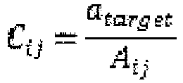
- the compensation factor matrix C ij may be calculated from a target critical dimension matrix a target and the distribution matrix A ij of critical dimension, so as to act as an exposure compensating parameter.
- the reflectivity or transmittance of a light valve array may be adjusted by a control device of the exposure device based on the compensation factor matrix C ij obtained in S2013, and each matrix element corresponds to one light valve unit of the light valve array.
- the optical transmittance or reflectivity of each light valve unit may be adjusted by adjusting an electrical signal applied to the light valve unit by way of a control device.
- the control device can purposefully adjust an electrical signal applied to each light valve unit according to the relationship and the compensation factor matrix C ij , and then the optical transmittance or reflectivity of light valve units is adjusted.
- the control device of the exposure device can adjust a voltage applied to each light valve unit of the exposure device according to the compensation factor matrix C ij and the relationship so as to adjust the optical transmittance of each light valve unit.
- the control device has purposefully adjusted the optical transmittance or reflectivity of each light valve unit according to the compensation factor matrix C ij , and thus light emitted by the exposure light source are adjusted in a region-dependent manner, the pattern obtained by performing an exposure process using the adjusted light gets closer to the desired target pattern, and the critical dimension in the obtained pattern is more uniform.
- acquisition of an exposure compensating parameter may further include the following operation S2014:
- the compensation factor matrix C jj is converted into the transmittance or reflectivity matrix T ij of the light valve array, and then the matrix T ij is used to adjust the optical transmittance or reflectivity of multiple light valve units of the exposure device.
- T max is the maximum transmittance of the optical valve units forming the light valve array
- max(C ij ) is the maximum value of each compensation factor
- T trans is a transmittance factor.
- the optical reflectivity matrix of the light valve array may be obtained similarly and useable for the subsequent compensating operation, and details are omitted here.
- adjustment of the optical transmittance or reflectivity of a plurality of light valve units of an exposure device with use of the optical transmittance or reflectivity matrix T ij includes that, the optical transmittance or reflectivity matrix T ij is made to correspond to the plurality of light valve units, so as to obtain the deviation of the optical transmittance or reflectivity of each light valve unit, and the optical transmittance or reflectivity of each light valve unit is adjusted according to the deviation.
- a calculation/conversion process from the distribution matrix of critical dimension A ij to a compensation factor matrix C ij and then to an optical transmittance or reflectivity matrix T ij as shown in FIG. 8 is executed by the control device (in the figure, contour maps of numerical values in the matrix A ij , matrix C ij and matrix T ij are illustratively given, and they represent the size distribution of values in the matrix), and the control device adjusts electrical signals applied to the plurality of light valve units of the exposure device.
- the light valve array is a transmissive light valve array
- a voltage applied to each light valve unit is adjusted so as to adjust the optical transmittance of each light valve unit.
- the pattern obtained by performing exposure with a compensating optical path that passes through the light valve array with adjusted transmittance has a more uniform critical dimension, as shown in FIG. 9 , and the critical dimension distribution matrix A correctedij of the finally obtained pattern is basically the same as the target critical dimension matrix a target or the error is within the acceptable range of the process.
- an exposure device, an exposure method and a lithography method which have at least one of the following beneficial effects:
Landscapes
- Physics & Mathematics (AREA)
- General Physics & Mathematics (AREA)
- Exposure And Positioning Against Photoresist Photosensitive Materials (AREA)
- Exposure Of Semiconductors, Excluding Electron Or Ion Beam Exposure (AREA)
Abstract
Description
- The present application claims priority to Chinese patent application No.
201710770859.4, filed on August 31, 2017 - Embodiments of the present disclosure relate to an exposure device, an exposure method and a photolithography method.
- In the fabrication process of semiconductor devices or display substrates, each functional layer is usually patterned by adopting a photolithography process. The critical dimension (CD) of a photolithography process refers to the minimum size of lines that can be formed by the photolithography process. The uniformity of the critical dimension of patterns formed by using the photolithography process usually affects characteristics of a product, so it is an important factor affecting quality of the product.
- At least an embodiment of the present disclosure provides an exposure device, comprising an exposure light source and an optical-path assembly, wherein the optical-path assembly is configured to guide light emitted by the exposure light source to an exposing position, the optical-path assembly comprises a light valve array, the light emitted by the exposure light source is able to be guided to the light valve array and then guided to the exposing position after the light is transmitted or reflected by the light valve array, the light valve array comprises a plurality of light valve units, and optical transmittance or reflectivity of each of the light valve units is adjustable.
- For example, in the exposure device provided by at least an embodiment of the present disclosure, the optical-path assembly comprises two light paths: a first exposure light path excluding the light valve array, and a second exposure light path comprising the light valve array.
- For example, in the exposure device provided by at least an embodiment of the present disclosure, the optical-path assembly further comprises a first reflect mirror and a second reflect mirror, the first reflect mirror is configured to guide the light emitted by the exposure light source to the light valve array, and the second reflect mirror is configured to guide the light subjected to transmission or reflection of the light valve array to the exposing position.
- For example, in the exposure device provided by at least an embodiment of the present disclosure, the light valve array is a reflective light valve array or a transmissive light valve array.
- For example, in the exposure device provided by at least an embodiment of the present disclosure, the reflective light valve array comprises a micromirror array; the transmissive light valve array comprises an electrochromic light valve array or a liquid crystal light valve array.
- For example, the exposure device provided by at least an embodiment of the present disclosure further comprises: a control device, configured to adjust the optical transmittance or reflectivity of each of the light valve units.
- For example, in the exposure device provided by at least an embodiment of the present disclosure, the electrochromic material adopted by the electrochromic light valve array comprises WO3, MoO, Nb2O5, V2O5, NiO, IrO or MnO.
- For example, in the exposure device provided by at least an embodiment of the present disclosure, the control device is configured to adjust the optical transmittance or reflectivity of each of the light valve units by adjusting a voltage applied to each light valve unit of the light valve array.
- For example, the exposure device provided by at least an embodiment of the present disclosure further comprises: a storage device, configured to store a relationship between a voltage applied to each of the light valve units and the optical transmittance or reflectivity of each of the light valve units.
- At least an embodiment of the present disclosure provides an exposure method using any one of the above exposure devices, comprising: acquiring an exposure compensating parameter; based on the exposure compensating parameter, adjusting reflectivity or transmittance of the light valve array; and performing exposure by the light that is emitted by the exposure light source and adjusted by the light valve array.
- For example, the exposure method provided by at least an embodiment of the present disclosure further comprises: prior to acquiring of the exposure compensating parameter, firstly judging whether or not an exposure pattern obtained by performing exposure without use of the light valve array meets a predetermined requirement, and in case of not meeting, then acquiring the exposure compensating parameter.
- For example, in the exposure method provided by at least an embodiment of the present disclosure, acquiring of the exposure compensating parameter comprises: obtaining a test pattern of critical dimension; getting a distribution matrix Aij of the critical dimension based on the test pattern; and calculating a compensating factor matrix Cij from a target critical dimension matrix atarget and the distribution matrix Aij of the critical dimension to function as the compensating parameter.
- For example, in the exposure method provided by at least an embodiment of the present disclosure, the compensating factor matrix Cij is calculated from the target critical dimension matrix atarget and the distribution matrix Aij of the critical dimension by the following formula:
- For example, in the exposure method provided by at least an embodiment of the present disclosure, the optical transmittance or reflectivity of a plurality of light valve units of the exposure device is adjusted according to the compensating factor matrix Cij, and the method further comprises: converting the compensating factor matrix Cij into an optical transmittance or reflectivity matrix Tij of the light valve array, and adjusting the optical transmittance or reflectivity of the plurality of light valve units of the exposure device with use of the optical transmittance or reflectivity matrix Tij.
- For example, in the exposure method provided by at least an embodiment of the present disclosure, when the light valve array is a transmissive light valve array, the compensating factor matrix Cij is converted into the transmittance matrix Tij of the light valve array by a following formula:

- For example, in the exposure method provided by at least an embodiment of the present disclosure, adjusting the optical transmittance or reflectivity of the plurality of light valve units of the exposure device with use of the optical transmittance or reflectivity matrix Tij comprises: letting the optical transmittance or reflectivity matrix Tij be correspondent with the plurality of light valve units, so as to obtain a deviation of optical transmittance or reflectivity of each of the light valve units, and adjusting the optical transmittance or reflectivity of each of the light valve units based on the deviation.
- For example, in the exposure method provided by at least an embodiment of the present disclosure, a control device of the exposure device adjusts a voltage of each of the light valve units of the exposure device according to a relationship between the voltage applied to the light valve units and the optical transmittance or reflectivity of the light valve units, so as to adjust the optical transmittance or reflectivity of each of the light valve units.
- For example, in the exposure method provided by at least an embodiment of the present disclosure, a distribution matrix Aij of the critical dimension is inputted into a control device of the exposure device, and the control device executes a calculation/conversion process, and adjusts voltage applied to a plurality of light valve units of the exposure device so as to adjust the optical transmittance or reflectivity of each of the light valve units.
- For example, in the exposure method provided by at least an embodiment of the present disclosure, the test pattern of critical dimension is a pattern obtained after a developing process; or the test pattern of critical dimension is a pattern obtained after an etching process.
- At least an embodiment of the present disclosure provides a photolithography method, comprising any one of the above-mentioned exposure methods.
- In order to clearly illustrate the technical solution of the embodiments of the disclosure, the drawings used in the description of the embodiments or relevant technologies will be briefly described in the following; it is obvious that the described drawings are only related to some embodiments of the disclosure and thus are not limitative of the disclosure.
-
FIG. 1A is a schematic view one illustrating an exposure device provided by an embodiment of the present disclosure; -
FIG. 1B is a schematically plan view illustrating a light valve array of an exposure device provided by an embodiment of the present disclosure; -
FIG. 2 is a schematic view two illustrating an exposure device provided by an embodiment of the present disclosure; -
FIG. 3 is a schematic view three illustrating an exposure device provided by an embodiment of the present disclosure; -
FIG. 4 is a schematic view four illustrating an exposure device provided by an embodiment of the present disclosure; -
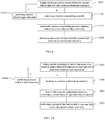
FIG. 5 is a flowchart one illustrating an exposure method provided by an embodiment of the present disclosure; -
FIG. 6 is a flowchart two illustrating an exposure method provided by an embodiment of the present disclosure; -
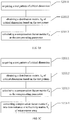
FIG. 7A is a flowchart illustrating a photolithography method provided by an embodiment of the present disclosure; -
FIG. 7B is a flowchart one illustrating acquisition of an exposure compensating parameter in a photolithography method provided by an embodiment of the present disclosure; -
FIG. 7C is a flowchart two illustrating acquisition of an exposure compensating parameter in a photolithography method provided by an embodiment of the present disclosure; -
FIG. 8 is a schematic view illustrating computational process of an exposure compensating parameter provided by an embodiment of the present disclosure; and -
FIG. 9 is a schematic view illustrating uniformity of pattern achieved by exposure compensation provided by an embodiment of the present disclosure. - 100 - workpiece to be processed; 201 - exposure light source; 202 - light valve array; 2020 - light valve unit; 203 - mask; 204 - first reflect mirror; 205 - second reflect mirror; 206 - control device; 207 - storage device
- In order to make objects, technical details and advantages of the embodiments of the disclosure apparent, the technical solutions of the embodiments will be described in a clearly and fully understandable way in connection with the drawings related to the embodiments of the disclosure. Apparently, the described embodiments are just a part but not all of the embodiments of the disclosure. Based on the described embodiments herein, those skilled in the art can obtain other embodiment(s), without any inventive work, which should be within the scope of the disclosure.
- Unless otherwise defined, all the technical and scientific terms used herein have the same meanings as commonly understood by one of ordinary skill in the art to which the present disclosure belongs. The terms "first," "second," etc., which are used in the description and the claims of the present application for disclosure, are not intended to indicate any sequence, amount or importance, but distinguish various components. Also, the terms such as "a," "an," etc., are not intended to limit the amount, but indicate the existence of at least one. The terms "comprise," "comprising," "include," "including," etc., are intended to specify that the elements or the objects stated before these terms encompass the elements or the objects and equivalents thereof listed after these terms, but do not preclude the other elements or objects. The phrases "connect", "connected", etc., are not intended to define a physical connection or mechanical connection, but may include an electrical connection, directly or indirectly. "On," "under," "right," "left" and the like are only used to indicate relative position relationship, and when the position of the object which is described is changed, the relative position relationship may be changed accordingly.
- As discovered by the inventor of the present disclosure in research, in a photolithography process, there are many factors affecting the uniformity of the patterns obtained through photolithographic such as uniformity of critical dimension, and these factors can be broadly divided into three categories. Firstly, the uniformity of critical dimension of patterns formed on a photomask, which directly affects the uniformity of critical dimension formed on a target product. Secondly, the uniformity of an exposing machine itself, for example, the uniformity of an exposure light source, lens, etc., has a direct effect on the uniformity of critical dimension formed on the target product. Thirdly, coating, development and etching of a photoresist and other procedures, which also have greater influence on the uniformity of critical dimension.
- However, methods to improve the uniformity of patterns obtained through photolithographic (e.g., the uniformity of critical dimension) available now often aim at just certain one of the above factors, for example only to improve to the photomask. For example, the light intensity transmitted by the photomask is controlled by forming various kinds of defects on a surface of the photomask or inside the photomask, but adjustment of the light intensity by using this method must involve recall of the photomask and improvement to the photomask, by way of an additional process. This process increases manufacturing cost of the photomask and takes a longer time, so the effects achievable by the method are limited.
- At least an embodiment of the present disclosure provides an exposure device, comprising an exposure light source and an optical-path assembly, wherein the optical-path assembly is configured to guide light emitted by the exposure light source to an exposing position, the optical-path assembly includes a light valve array, light emitted by the exposure light source is able to be guided to the light valve array, and then guided to the exposing position after the light is transmitted or reflected by the light valve array, the light valve array includes a plurality of light valve units, optical transmittance or reflectivity of each of the light valve units is adjustable.
- At least an embodiment of the present disclosure provides an exposure method using the above exposure device, and the method comprises: acquiring an exposure compensating parameter; based on the exposure compensating parameter, adjusting the reflectivity or transmittance of the light valve array; performing exposure by the light that is emitted by the exposure light source and adjusted by the light valve array.
- At least an embodiment of the present disclosure provides a photolithography method that comprises the exposure method.
- Hereinafter, the exposure device, exposure method and photolithography method of the present disclosure will be described with aid of several specific embodiments.
- According to the present embodiment, there is provided an exposure device, and as shown in
FIG. 1A andFIG. 2 , the exposure device includes an exposurelight source 201 and an optical-path assembly. The optical-patch assembly is configured to guide the light emitted by the exposurelight source 201, via anexposure mask 203, to an exposing position, for exposing a photoresist layer that has been coated on aworkpiece 100 to be processed (e.g., a substrate or wafer) placed at the exposing position; the optical-path assembly includes alight valve array 202, and the light emitted by the exposurelight source 201 can be guided to thelight valve array 202, and then be guided to the exposing position after being transmitted or reflected by thelight valve array 202. As shown inFIG. 1B , thelight valve array 202 can include a plurality oflight valve units 2020, and optical transmittance or reflectivity of theselight valve units 2020 can be adjusted so that the light intensity arriving at thelight valve array 202 can be adjusted separately. - For example, in this embodiment, the optical transmittance or reflectivity of each
light valve unit 2020 of thelight valve array 202 in the optical-path assembly may be adjusted, and so thelight valve array 202 can selectively transmit or reflect the light emitted by the exposurelight source 201 in a region-dependent manner, so as to control the final intensity and distribution of the light guided to the exposing position in the exposure device. In this embodiment, for example, the position of eachlight valve unit 2020 of thelight valve array 202 may also be adjusted (e.g., the tilt angle of eachlight valve unit 2020 or the like may be adjusted, so as to adjust the propagating direction of light and guide light to the exposing position accurately. - In the present embodiment, the optical-path assembly of the exposure device may include two light paths; one light path is an ordinary light path, that is, a first exposure light path which excludes the
light valve array 202, in which the exposurelight source 201 can be directly used for exposure; and the other light path is a compensating light path, that is, a second exposure light path comprising thelight valve array 202, by which light from the exposurelight source 201 can be adjusted so as to control the final exposure intensity and distribution of the exposure device. In this embodiment, two light paths may, for example, be separately arranged in different areas of the exposure device, so different light paths may be selected for exposure according to requirements. For another example, two light paths may share at least part of a light path channel, and in this case thelight valve array 202 may be arranged to be a detachable structure and be selectively mounted according to exposure requirements. When the second exposure light path including thelight valve array 202 is required for exposure, thelight valve array 202 may be installed in the light path channel; when the first exposure light path excluding thelight valve array 202 is required to be used for exposure, thelight valve array 202 in the light path channel may be detached. - In another example of this embodiment, as shown in
FIG.1 , the exposure device includes an exposurelight source 201, alight valve array 202, and may further include, for example, a mask carrier (not shown) provided at the light exit of the exposure device, and amask 203 is detachably mounted on the mask carrier. In this example, thelight valve array 202 is a transmissive light valve array, and light emitted by the exposurelight source 201 are guided to aworkpiece 100 to be processed that is placed at an exposing position after the light is transmitted by thelight valve array 202. The exposure device utilizes each light valve unit of thelight valve array 202 to selectively transmit light emitted by the exposurelight source 201, thereby achieving the technical effect of controlling the final exposure intensity and distribution of the exposure device. In this example, the exposure device may further include, for example, a lens assembly (not shown in the figure) and so on, and the lens assembly may be mounted, for example, between the exposurelight source 201 and thelight valve array 202 to assist in adjusting the light emitted by the exposurelight source 201. - In another example of this embodiment, as shown in
FIG. 2 , the exposure device also includes an exposurelight source 201, alight valve array 202, and a mask carrier (not shown) arranged at the light exit of the exposure device for detachable installation of amask 203. Unlike the previous example, in this example, thelight valve array 202 is a reflective light valve array, and an optical-path assembly of the exposure device further includes afirst reflect mirror 204 and asecond reflect mirror 205. Light emitted by the exposurelight source 201 are led by thefirst reflect mirror 204 to thelight valve array 202, and the light reflected by thelight valve array 202 are led by thesecond reflect mirror 205 to aworkpiece 100 to be processed that is placed in an exposing position. The exposure device utilizes each light valve unit of thelight valve array 202 to selectively reflect light emitted by the exposurelight source 201, thereby achieving the technical effect of controlling the final exposure intensity and distribution of the exposure device. In this example, the exposure device may further include a lens assembly or the like (not shown in the figure) likewise, and the lens assembly may be mounted, for example, between the exposurelight source 201 and thefirst reflect mirror 204 or at other suitable location so as to make auxiliary adjustment of the light emitted by the exposurelight source 201. - In the exposure device, the exposure
light source 201 may be selected as required to be a light source with appropriate wavelength, and for example, it may be a light source of G-line (436 nm) in ultraviolet spectrum, i-line (365 nm) developed to 248 nm, 193 nm, extreme ultraviolet light (EUV) or even X-ray, etc. - In this example, the
first reflect mirror 204 and thesecond reflect mirror 205 may be selectively installed, and the number, mounting position and installation angle of thefirst reflect mirror 204 and thesecond reflect mirror 205 may be adjusted according to the required exposure position. For example, when thefirst reflect mirror 204 and thesecond reflect mirror 205 are not installed, light emitted by the exposurelight source 201 does not pass through thelight valve array 202, the exposure light path in this case is the first exposure light path that excludes thelight valve array 202; when thefirst reflect mirror 204 and thesecond reflect mirror 205 are installed, light emitted by the exposurelight source 201 are guided by thefirst reflect mirror 204 to thelight valve array 202, and is then reflected to the exposure position by thesecond reflect mirror 205 after the light is modulated by thelight valve array 202, the exposure light path at this time is the second exposure light path that includes thelight valve array 202. In this example, according to positional relationship between the exposure device and the exposure position as well as mounting position of thelight valve array 202, onefirst reflect mirror 204 is provided, twosecond reflect mirror 205 is provided, and the installation as shown inFIG. 2 is carried out. The reflect mirrors may be plane mirrors, or when scaling or other operation is required, may be curved mirrors, such as concave mirrors, convex mirrors or the like. The position of each light valve unit of thelight valve array 202 may be adjusted as well, so that the light reflected by thelight valve array 202 can be directed to the exposure position. - As described above, in the embodiments, the light valve array may be for example a reflective light valve array or a transmissive light valve array, and the type may be selected according to demand.
- The reflective light valve array may, for example, be a micromirror array, such as a digital micromirror array, such as a high-reflectivity aluminum micromirror array, and optical reflectivity of the micromirror array may be adjusted with digital signals, thereby modulating the incident light emitted from the light source according to the signals. The micromirror array is such as an MEMS (micro-electromechanical system) type micromirror array. The basic principle of the MEMS type micromirror array is to cause a movable micromirror to rotate or translate under the action of static electricity (or magnetic force), so that the propagating direction or phase of input light can be changed.
- The transmissive light valve array may be, for example, an electrochromic light valve array, a liquid crystal light valve array or the like. The electrochromic material used in the electrochromic light valve array may be, for example, WO3, MoO, Nb2O5, V2O5, NiO, IrO, MnO or the like, and this embodiment places no limitation on the specific category of the electrochromic material. The optical transmittance of these materials can be adjusted with the aid of the magnitude of an externally applied voltage. For example, an electrochromic light valve array includes two substrates opposed to each other, with a layer of electrochromic material interposed therebetween. At least one of the two substrates may be an array substrate, on which a corresponding drive array is provided, while the other substrate is an opposing substrate, on which a common electrode is arranged. The drive array includes a plurality of pixel units; each of the pixel units can correspond to one light valve unit, and includes such as a thin film transistor, a pixel electrode, and other circuital structure. The pixel electrode and a common electrode of each of the light valve units can act to apply a voltage difference across the electrochromic material of the corresponding part so as to change its transmittance. The liquid crystal light valve array can act to control the rotational angle of liquid crystal molecules with the aid of an electrical signal and then the transmittance of light is adjusted.
- For example, the liquid crystal light valve array includes two substrates opposed to each other, with a layer of liquid crystal material interposed therebetween, and the two substrates are respectively provided with two polarizers, the polarizing axes of which are perpendicular to each other. At least one of the two substrates may be an array substrate, on which a corresponding drive array is provided, while the other substrate is an opposing substrate, on which a common electrode is arranged. The drive array includes a plurality of pixel units, each of which may correspond to one light valve unit, and include such as a thin film transistor, a pixel electrode, and other circuital structure. The pixel electrode and a common electrode of each of the light valve units can act to apply a voltage difference to the liquid crystal material of the corresponding part so as to change its transmittance.
- In this embodiment, as shown in
FIG. 3 , the exposure device may further include acontrol device 206 which may be, for example, electrically connected to thelight valve array 202, and be configured to provide thelight valve array 202 with display signals so as to adjust the optical transmittance or reflectivity of thelight valve array 202. For example, thecontrol device 206 may be configured to be capable of adjusting the optical transmittance or reflectivity of each light valve unit in thelight valve array 202. For example, when thelight valve array 202 is an electrochromic light valve array, thecontrol device 206 may be configured to adjust the optical transmittance of each light valve unit by adjusting a voltage applied to each light valve unit in thelight valve array 202. The controller may be in various forms such as a central processor, a microprocessor, a programmable logic controller (PLC) and so on, and is configured to be able to execute a computer program or instructions, and the embodiments of the present disclosure place no limitation on this aspect. - In this embodiment, as shown in
FIG. 4 , the exposure device may further include astorage device 207, which may, for example, store a relationship between an electrical signal applied to a light valve unit and the optical transmittance or reflectivity of the light valve unit. In this way, thecontrol device 206 makes an individualized adjustment to an electrical signal applied to each light valve unit according to the relationship, and then the optical transmittance or reflectivity of the light valve unit is adjusted. For example, when thelight valve array 202 is an electrochromic light valve array, thestorage device 207 may store the relationship between a voltage applied to a light valve unit and the optical transmittance of the light valve unit. Thus, thecontrol device 206 can adjust the voltage applied to each light valve unit according to the relationship, and then the optical transmittance of each light valve unit is adjusted. Thestorage device 207 may include a magnetic storage medium, a semiconductor storage medium, or the like, and may be a volatile storage device or a non-volatile storage device, and the embodiments of the present disclosure place no limitation on in this aspect. - The exposure device provided by this embodiment may be used, for example, in a photolithography process, and thus the light emitted by the exposure
light source 201 may be useful for exposure by means of selectively utilizing a normal light path or a compensating light path, then light exiting from the exposure device is illuminated to an exposing position via amask 203, for example, to aworkpiece 100 to be processed such as a substrate, wafer or the like, thereby realizing patterning on theworkpiece 100 to be processed. When a compensating light path is utilized for exposure in the exposure device provided by the present embodiment, the technical effect of controlling the final exposure amount of the exposure device in a region-dependent manner can be achieved by adjusting the optical transmittance or reflectivity of each light valve unit in thelight valve array 202. When the exposure device is used in photolithography process, the photolithographic pattern can be made to be more uniform, or closer to the desired target pattern. - According to the present embodiment, there is provided an exposure method by employing any of the above exposure devices for exposure, by which, the exposure process can be compensated, so as to obtain an exposure pattern that is more uniform or closer to the desired target pattern. Thus, quality of the patterning process is improved. As shown in
FIG. 5 , the method includes the following operations S101∼S103. - S 101: acquiring an exposure compensating parameter.
- In this embodiment, an exposure compensating parameter may be acquired, for example, by a test pattern obtained after an exposure process is performed once. The test pattern may be, for example, a pattern obtained after performing a development process, or may also be a pattern obtained after performing an etching process. By comparing the test pattern with a target pattern desired to be obtained, the difference between the test pattern and the target pattern and the difference degree are obtained, and then an exposure compensating parameter is obtained. The exposure compensating parameter may be, for example, a numerical value, and may also be a numerical matrix, and its concrete form is not limited here.
- S102: adjusting the reflectivity or transmittance of the light valve array according to the exposure compensating parameter.
- In this embodiment, for example, the reflectivity or transmittance of the light valve array may be adjusted by a control device of the exposure device according to the exposure compensating parameter, and for example, the optical transmittance or reflectivity of each light valve unit may be adjusted by adjusting an electrical signal applied to the light valve unit with use of the control device. When the relationship between an electrical signal applied to a light valve unit and the optical transmittance or optical reflectivity of the light valve unit is stored in a storage device of the exposure device, the control device can make an individualized adjustment to an electrical signal applied to each light valve unit according to the relationship and the exposure compensating parameter, and then the optical transmittance or reflectivity of each light valve unit is adjusted. For example, when the light valve array is an electro chromic light valve array and the relationship between a voltage applied to a light valve unit and the optical transmittance of the light valve unit is stored in a storage device, the control device of the exposure device can adjust the size of a voltage applied to each light valve unit according to the relationship and the exposure compensating parameter purposefully and respectively so as to adjust transmittance of each light valve unit.
- S103: using light that is emitted from the exposure light source and has been adjusted by the light valve array for exposure.
- In the present embodiment, because the optical transmittance or reflectivity of each light valve unit of the light valve array is adjusted purposefully by the control device according to the exposure compensating parameter, and then the light emitted by the exposure light source is adjusted, the pattern obtained by performing an exposure process with the adjusted light get closer to the desired target pattern. For example, a photoresist layer subjected to exposure is developed to obtain a photoresist pattern, which can be used as an etching mask, to etch other structural layers beneath the photoresist layer. The etching process may be either dry etching or wet etching.
- In another example of this embodiment, as shown in
FIG. 6 , the exposure method further includes an operation S100 prior to the operation S101. - S 100: judging whether or not an exposure pattern in the case of performing an exposure without use of a light valve array meets a predetermined requirement.
- The judging process is usually performed before the step S101, i.e., prior to acquiring of the exposure compensating parameter. When the obtained result is a positive result, that is, when an exposure pattern in the case of performing an exposure without use of a light valve array meets a predetermined requirement, exposure can be carried out using an ordinary optical path of the exposure device. Namely, the process advance to the step S101*, in which exposure is performed using the first exposure light path that does not include a light valve array. When the obtained result is a negative result, that is, when an exposure pattern in the case of performing an exposure without use of a light valve array does not meet a predetermined requirement, exposure can be carried out by using a compensating optical path of the exposure device. Namely, the process switches to the step S101, exposure is performed by using a second exposure light path that includes a light valve array, and at this time an exposure compensating parameter is further acquired.
- According to the present embodiment, there is provided an exposure method, which may be, for example, used in a photolithography process to obtain a uniform critical dimension. The photolithography process includes, for example, coating of a photoresist, exposing the photoresist by using the exposure method provided by the present embodiment, developing treatment of the photoresist to obtain a photoresist pattern, transferring of the photoresist pattern to the required material so as to obtain a photolithographic pattern on the material, etc.. In the present embodiment, the exposure method provided by embodiments of the present disclosure will be described with reference to an example in which the uniformity of critical dimension of photolithographic patterns is achieved.
- In the present embodiment, as shown in
FIG. 7A , the exposure method includes steps S200 to S203. - S200: judging whether or not the critical dimension of an exposure pattern obtained in the case of performing exposure without use of a light valve array meets a predetermined requirement.
- In the present embodiment, for example, a test pattern of critical dimension may be obtained firstly, and the pattern may be such as a pattern obtained after a development process, and may also be a pattern obtained after an etching process. The test pattern can reflect the distribution of size of the critical dimension. According to the uniformity of critical dimension in the test pattern of critical dimension, it is judged whether or not a pattern obtained in the case of performing exposure without use of a light valve array meets a predetermined requirement. For example, it is measured whether or not the critical dimension at each location in the test pattern of critical dimension exceeds a preset maximum critical dimension, or whether or not the difference between the maximum critical dimension and the minimum critical dimension in the test pattern exceeds the process requirement. When the obtained uniformity of critical dimension in the test pattern of critical dimension meets the standard, that is, when the judgment result is positive, an ordinary light path of the exposure device can be used for exposure. Namely, the process goes to step S201*, exposure is performed by using the first exposure light path excluding a light valve array. Conversely, when the obtained uniformity of critical dimension in the test pattern of critical dimension does not meet the standard, that is, when the obtained result is negative, a compensating light path of the exposure device can be used for exposure. Namely, the process goes to step S201, exposure is performed using a second exposure light path including a light valve array.
- S201, acquiring an exposure compensating parameter.
- As shown in
FIG. 7B , in an example, acquisition of the exposure compensating parameter includes operations S2011 to S2013. - S2011, obtaining a test pattern of critical dimension.
- In this embodiment, the test pattern may be the test pattern of critical dimension obtained in step S200, and may also be a test pattern of critical dimension obtained newly. In order to simplify process and save time, the test pattern of critical dimension obtained in step S200 is selected in this embodiment, and this test pattern can reflect the influence of each step in the exposure process on the exposure pattern.
- S2012: obtaining a distribution matrix Aij of critical dimension based on the test pattern.
- In this embodiment, for example, an automatic optical detection device can be used to detect the size of the critical dimension at each location in the test pattern, and then a distribution matrix Aij of critical dimension is generated.
- S2013: obtaining a compensation factor matrix Cij by calculation.
- In this embodiment, for example, the compensation factor matrix Cij may be calculated from a target critical dimension matrix atarget and the distribution matrix Aij of critical dimension, so as to act as an exposure compensating parameter. In this embodiment, for example, the compensation factor matrix Cij may be obtained by calculation with the following formula:

- S202: adjusting the reflectivity or transmittance of the light valve array according to the exposure compensating parameter.
- In this embodiment, for example, the reflectivity or transmittance of a light valve array may be adjusted by a control device of the exposure device based on the compensation factor matrix Cij obtained in S2013, and each matrix element corresponds to one light valve unit of the light valve array. For example, the optical transmittance or reflectivity of each light valve unit may be adjusted by adjusting an electrical signal applied to the light valve unit by way of a control device. When the relationship between an electrical signal applied to a light valve unit and the optical transmittance or reflectivity of the light valve unit is stored in a storage device of the exposure device, the control device can purposefully adjust an electrical signal applied to each light valve unit according to the relationship and the compensation factor matrix Cij, and then the optical transmittance or reflectivity of light valve units is adjusted.
- For example, when the light valve array is a transmissive light valve array, and the relationship between a voltage applied to a light valve unit and the optical transmittance of the light valve unit is stored in the storage device, the control device of the exposure device can adjust a voltage applied to each light valve unit of the exposure device according to the compensation factor matrix Cij and the relationship so as to adjust the optical transmittance of each light valve unit.
- S203: using light emitted from the exposure source and adjusted by the light valve array for exposure.
- In the present embodiment, in view of the fact that the control device has purposefully adjusted the optical transmittance or reflectivity of each light valve unit according to the compensation factor matrix Cij, and thus light emitted by the exposure light source are adjusted in a region-dependent manner, the pattern obtained by performing an exposure process using the adjusted light gets closer to the desired target pattern, and the critical dimension in the obtained pattern is more uniform.
- In another example of this embodiment, as shown in
FIG. 7C , based on the example shown inFIG. 7B , acquisition of an exposure compensating parameter may further include the following operation S2014: - S2014: converting the compensation factor matrix Cij into an optical transmittance or reflectivity matrix Tij of the light valve array.
- In this example, it is possible that the compensation factor matrix Cjj is converted into the transmittance or reflectivity matrix Tij of the light valve array, and then the matrix Tij is used to adjust the optical transmittance or reflectivity of multiple light valve units of the exposure device. For example, when the light valve array is a transmissive light valve array, the compensation factor matrix Cij may be converted into the optical transmittance matrix Tij of the light valve array by the following formula:

- In the present embodiment, adjustment of the optical transmittance or reflectivity of a plurality of light valve units of an exposure device with use of the optical transmittance or reflectivity matrix Tij includes that, the optical transmittance or reflectivity matrix Tij is made to correspond to the plurality of light valve units, so as to obtain the deviation of the optical transmittance or reflectivity of each light valve unit, and the optical transmittance or reflectivity of each light valve unit is adjusted according to the deviation.
- In this embodiment, for example, it is possible that by way of inputting a distribution matrix Aij of critical dimension into a control device of the exposure device, a calculation/conversion process from the distribution matrix of critical dimension Aij to a compensation factor matrix Cij and then to an optical transmittance or reflectivity matrix Tij as shown in
FIG. 8 is executed by the control device (in the figure, contour maps of numerical values in the matrix Aij, matrix Cij and matrix Tij are illustratively given, and they represent the size distribution of values in the matrix), and the control device adjusts electrical signals applied to the plurality of light valve units of the exposure device. For example, when the light valve array is a transmissive light valve array, a voltage applied to each light valve unit is adjusted so as to adjust the optical transmittance of each light valve unit. The pattern obtained by performing exposure with a compensating optical path that passes through the light valve array with adjusted transmittance has a more uniform critical dimension, as shown inFIG. 9 , and the critical dimension distribution matrix Acorrectedij of the finally obtained pattern is basically the same as the target critical dimension matrix atarget or the error is within the acceptable range of the process. - According to at least one embodiment of the present disclosure, there are provided an exposure device, an exposure method and a lithography method, which have at least one of the following beneficial effects:
- (1) An exposure device provided by an embodiment of the present disclosure has two optical paths, and upon exposure, a normal light path or a compensating light path with a light valve array can be selected for an exposure process according to actual situations, thereby improving exposure quality of the exposure device.
- (2) A compensating light path possessed by an exposure device provided in an embodiment of the present disclosure can make use of a light valve array to adjust light emitted by an exposure light source, the light valve array having a plurality of light valve units, and therefore, the technical effect of adjusting the final exposure amount of the exposure device in a region-dependent manner can be achieved.
- (3) Regarding an exposure method provided by an embodiment of the present disclosure, an exposure compensating parameter can be obtained based on a test pattern, and is useful for adjusting the optical transmittance or reflectivity of each light valve unit of the light valve array of the exposure device to control the fmal exposure amount of the exposure device, so that the obtained exposure pattern is closer to the desired target pattern and uniformity of the exposure pattern is improved.
- (4) An exposure method provided by an embodiment of the present disclosure can be used in a photolithography process, an exposure compensating parameter can be acquired by the exposure method based on a test pattern, which reflects influences of various factors such as a photomask, an exposure device, a development process, a photolithography process and the like on the final photolithographic pattern, and therefore, by means of using the exposure compensating parameter to control the final exposure amount of the exposure device, the obtained photolithographic pattern can be made to get closer to the desired target pattern. Consequently, the uniformity of photolithographic patterns is improved, and for example, uniformity of the critical dimension of photolithographic patterns is improved.
- The following statements should be noted:
- (1) The accompanying drawings involve only the structure(s) in connection with the embodiment(s) of the present disclosure, and other structure(s) can be referred to common design(s).
- (2) For the purpose of clarity only, in accompanying drawings for illustrating the embodiment(s) of the present disclosure, the thickness and size of a layer or a structure may be enlarged. However, it should understood that, in the case in which a component or element such as a layer, film, area, substrate or the like is referred to be "on" or "under" another component or element, it may be directly on or under the another component or element or a component or element is interposed therebetween.
- (3) In case of no conflict, features in one embodiment or in different embodiments can be combined.
- What are described above involves the illustrative embodiments of the disclosure only and not limitative to the scope of the disclosure. The modification or substitution which can be conceived by those skilled in the art related to the present disclosure should be in the protection scope of the present disclosure. The scopes of the present disclosure are defined by the accompanying claims.
Claims (20)
- An exposure device, comprising an exposure light source and an optical-path assembly,
wherein the optical-path assembly is configured to guide light emitted by the exposure light source to an exposing position,
the optical-path assembly comprises a light valve array, the light emitted by the exposure light source is able to be guided to the light valve array and then guided to the exposing position after the light is transmitted or reflected by the light valve array,
the light valve array comprises a plurality of light valve units, and optical transmittance or reflectivity of each of the light valve units is adjustable. - The exposure device as claimed in claim 1, wherein the optical-path assembly comprises two light paths:a first exposure light path excluding the light valve array, anda second exposure light path comprising the light valve array.
- The exposure device as claimed in claim 1 or 2, wherein the optical-path assembly further comprises a first reflect mirror and a second reflect mirror,
the first reflect mirror is configured to guide the light emitted by the exposure light source to the light valve array, and
the second reflect mirror is configured to guide the light subjected to transmission or reflection of the light valve array to the exposing position. - The exposure device as claimed in any one of claims 1 to 3, wherein the light valve array is a reflective light valve array or a transmissive light valve array.
- The exposure device as claimed in claim 4, wherein the reflective light valve array comprises a micromirror array;
the transmissive light valve array comprises an electrochromic light valve array or a liquid crystal light valve array. - The exposure device as claimed in any one of claims 1 to 5, further comprising:
a control device, configured to adjust the optical transmittance or reflectivity of each of the light valve units. - The exposure device as claimed in claim 5, wherein an electrochromic material adopted by the electrochromic light valve array comprises WO3, MoO, Nb2O5, V2O5, NiO, IrO or MnO.
- The exposure device as claimed in claim 6, wherein the control device is configured to adjust the optical transmittance or reflectivity of each of the light valve units by adjusting a voltage applied to each light valve unit of the light valve array.
- The exposure device as claimed in any one of claims 1 to 8, further comprising:
a storage device, configured to store a relationship between a voltage applied to each of the light valve units and the optical transmittance or reflectivity of each of the light valve units. - An exposure method using the exposure device as claimed in any one of claims 1 to 9, comprising:acquiring an exposure compensating parameter;based on the exposure compensating parameter, adjusting reflectivity or transmittance of the light valve array; andperforming exposure by the light that is emitted by the exposure light source and adjusted by the light valve array.
- The exposure method as claimed in claim 10, further comprising:
prior to acquiring of the exposure compensating parameter, firstly judging whether or not an exposure pattern obtained by performing exposure without use of the light valve array meets a predetermined requirement, and in case of not meeting, then acquiring the exposure compensating parameter. - The exposure method as claimed in claim 10 or 11, wherein acquiring of the exposure compensating parameter comprises:obtaining a test pattern of critical dimension;getting a distribution matrix Aij of the critical dimension based on the test pattern; andcalculating a compensating factor matrix Cij from a target critical dimension matrix atarget and the distribution matrix Aij of the critical dimension to function as the compensating parameter.
- The exposure method as claimed in claim 12, wherein the compensating factor matrix Cij is calculated from the target critical dimension matrix atarget and the distribution matrix Aij of the critical dimension by the following formula:

- The exposure method as claimed in claim 13, wherein the optical transmittance or reflectivity of a plurality of light valve units of the exposure device is adjusted according to the compensating factor matrix Cij, and
the method further comprises:
converting the compensating factor matrix Cij into an optical transmittance or reflectivity matrix Tij of the light valve array, and adjusting the optical transmittance or reflectivity of the plurality of light valve units of the exposure device with use of the optical transmittance or reflectivity matrix Tij. - The exposure method as claimed in claim 14, wherein when the light valve array is a transmissive light valve array, the compensating factor matrix Cij is converted into the transmittance matrix Tij of the light valve array by a following formula:

- The exposure method as claimed in claim 14, wherein adjusting the optical transmittance or reflectivity of the plurality of light valve units of the exposure device with use of the optical transmittance or reflectivity matrix Tij comprises:
letting the optical transmittance or reflectivity matrix Tij be correspondent with the plurality of light valve units, so as to obtain a deviation of optical transmittance or reflectivity of each of the light valve units, and adjusting the optical transmittance or reflectivity of each of the light valve units based on the deviation. - The exposure method as claimed in claim 11, wherein a control device of the exposure device adjusts a voltage of each of the light valve units of the exposure device according to a relationship between the voltage applied to the light valve units and the optical transmittance or reflectivity of the light valve units, so as to adjust the optical transmittance or reflectivity of each of the light valve units.
- The exposure method as claimed in claim 14, wherein a distribution matrix Aij of the critical dimension is inputted into a control device of the exposure device, and
the control device executes a calculation/conversion process, and adjusts voltage applied to a plurality of light valve units of the exposure device so as to adjust the optical transmittance or reflectivity of each of the light valve units. - The exposure method as claimed in claim 12, wherein the test pattern of critical dimension is a pattern obtained after a developing process; or
the test pattern of critical dimension is a pattern obtained after an etching process. - A photolithography method, comprising the exposure method as claimed in any one of claims 10 to 19.
Applications Claiming Priority (2)
| Application Number | Priority Date | Filing Date | Title |
|---|---|---|---|
| CN201710770859.4A CN109426091B (en) | 2017-08-31 | 2017-08-31 | Exposure apparatus, exposure method, and photolithography method |
| PCT/CN2018/080768 WO2019041796A1 (en) | 2017-08-31 | 2018-03-28 | Exposure device, exposure method, and photolithography method |
Publications (2)
| Publication Number | Publication Date |
|---|---|
| EP3677966A1 true EP3677966A1 (en) | 2020-07-08 |
| EP3677966A4 EP3677966A4 (en) | 2021-06-09 |
Family
ID=65505263
Family Applications (1)
| Application Number | Title | Priority Date | Filing Date |
|---|---|---|---|
| EP18772701.1A Withdrawn EP3677966A4 (en) | 2017-08-31 | 2018-03-28 | EXPOSURE DEVICE, EXPOSURE PROCESS AND PHOTOLITHOGRAPHY PROCESS |
Country Status (5)
| Country | Link |
|---|---|
| US (1) | US11294288B2 (en) |
| EP (1) | EP3677966A4 (en) |
| JP (1) | JP7246928B2 (en) |
| CN (1) | CN109426091B (en) |
| WO (1) | WO2019041796A1 (en) |
Family Cites Families (34)
| Publication number | Priority date | Publication date | Assignee | Title |
|---|---|---|---|---|
| JPS61190935A (en) | 1985-02-20 | 1986-08-25 | Hitachi Ltd | Exposing device |
| JPS62203133A (en) | 1986-03-03 | 1987-09-07 | Canon Inc | optical modulation element |
| JPH1032160A (en) * | 1996-07-17 | 1998-02-03 | Toshiba Corp | Pattern exposure method and exposure apparatus |
| SE9800665D0 (en) | 1998-03-02 | 1998-03-02 | Micronic Laser Systems Ab | Improved method for projection printing using a micromirror SLM |
| US6262795B1 (en) | 1998-08-28 | 2001-07-17 | Philip Semiconductors, Inc. | Apparatus and method for the improvement of illumination uniformity in photolithographic systems |
| US6998219B2 (en) * | 2001-06-27 | 2006-02-14 | University Of South Florida | Maskless photolithography for etching and deposition |
| JP2004012899A (en) * | 2002-06-07 | 2004-01-15 | Fuji Photo Film Co Ltd | Aligner |
| CN1997878A (en) | 2003-07-18 | 2007-07-11 | Uclt有限责任公司 | Method for correcting critical dimension variations in photomasks |
| JP4599936B2 (en) * | 2004-08-17 | 2010-12-15 | 株式会社ニコン | Illumination optical apparatus, adjustment method of illumination optical apparatus, exposure apparatus, and exposure method |
| JP2006108465A (en) | 2004-10-07 | 2006-04-20 | Nikon Corp | Optical characteristic measuring apparatus and exposure apparatus |
| CN2795900Y (en) * | 2005-01-05 | 2006-07-12 | 中国科学院长春光学精密机械与物理研究所 | Self control liquid crystal light valve group photo etching shutter mechanism |
| WO2006085626A1 (en) | 2005-02-14 | 2006-08-17 | Nikon Corporation | Exposure method and system, and method for fabricating device |
| WO2006104173A1 (en) * | 2005-03-28 | 2006-10-05 | Fujifilm Corporation | Light quantity adjustment method, image recording method, and device |
| US8137870B2 (en) | 2005-06-14 | 2012-03-20 | Samsung Electronics Co., Ltd. | Method of manufacturing photomask |
| KR100604940B1 (en) | 2005-06-14 | 2006-07-28 | 삼성전자주식회사 | Apparatus for measuring photo mask, method for measuring photo mask using same, apparatus and method for calibrating photo mask using CD, and method for manufacturing photo mask |
| JP2007140166A (en) * | 2005-11-18 | 2007-06-07 | Shinko Electric Ind Co Ltd | Direct exposure apparatus and illuminance adjustment method |
| KR100694664B1 (en) | 2006-02-15 | 2007-03-13 | 삼성전자주식회사 | Light intensity control method and apparatus and semiconductor substrate exposure apparatus and method |
| KR20090021755A (en) | 2007-08-28 | 2009-03-04 | 삼성전자주식회사 | Exposure apparatus and exposure method of semiconductor substrate |
| US8451427B2 (en) * | 2007-09-14 | 2013-05-28 | Nikon Corporation | Illumination optical system, exposure apparatus, optical element and manufacturing method thereof, and device manufacturing method |
| US20090091730A1 (en) | 2007-10-03 | 2009-04-09 | Nikon Corporation | Spatial light modulation unit, illumination apparatus, exposure apparatus, and device manufacturing method |
| JP2010004008A (en) | 2007-10-31 | 2010-01-07 | Nikon Corp | Optical unit, illumination optical device, exposure apparatus, exposure method and production process of device |
| JP2010016351A (en) | 2008-06-03 | 2010-01-21 | Seiko Epson Corp | Liquid crystal blind, method of manufacturing semiconductor device using the same, and reduced projection exposure apparatus for semiconductor manufacture |
| KR101692265B1 (en) * | 2009-12-08 | 2017-01-04 | 삼성전자 주식회사 | Maskless exposure apparatus and pattern compensating method using the same |
| WO2012060099A1 (en) * | 2010-11-04 | 2012-05-10 | 株式会社ニコン | Light source adjustment method, exposure method, device manufacturing method, illumination optical system, and exposure device |
| EP2618201B1 (en) * | 2012-01-20 | 2015-11-04 | Imec | Calibration of micro-mirror arrays |
| CN103809382B (en) * | 2012-11-06 | 2015-11-18 | 上海微电子装备有限公司 | For lithographic equipment even smooth regulating device and use the illuminator of this device |
| CN203376558U (en) * | 2013-08-12 | 2014-01-01 | 中山新诺科技有限公司 | Device carrying out uniformity compensation in scanning direction |
| KR102153599B1 (en) * | 2013-11-18 | 2020-09-08 | 삼성전자주식회사 | Head mounted display apparatus and method for changing a light transmittance |
| CN203825292U (en) * | 2014-05-09 | 2014-09-10 | 中芯国际集成电路制造(北京)有限公司 | Variable attenuator device |
| CN104216177A (en) * | 2014-08-01 | 2014-12-17 | 京东方科技集团股份有限公司 | Display panel, display device and preparation method of display panel |
| JP6636323B2 (en) * | 2015-12-28 | 2020-01-29 | 株式会社日立エルジーデータストレージ | Dimmer and image display device using the same |
| CN106933049B (en) * | 2015-12-30 | 2020-06-16 | 上海微电子装备(集团)股份有限公司 | Exposure system and exposure method for semiconductor photoetching |
| KR102672027B1 (en) * | 2016-12-20 | 2024-06-03 | 에베 그룹 에. 탈너 게엠베하 | Device and method for exposing a light-sensitive layer |
| CN206479771U (en) * | 2017-02-28 | 2017-09-08 | 京东方科技集团股份有限公司 | A kind of proximity printing device |
-
2017
- 2017-08-31 CN CN201710770859.4A patent/CN109426091B/en active Active
-
2018
- 2018-03-28 JP JP2018552056A patent/JP7246928B2/en active Active
- 2018-03-28 US US16/090,740 patent/US11294288B2/en not_active Expired - Fee Related
- 2018-03-28 WO PCT/CN2018/080768 patent/WO2019041796A1/en not_active Ceased
- 2018-03-28 EP EP18772701.1A patent/EP3677966A4/en not_active Withdrawn
Also Published As
| Publication number | Publication date |
|---|---|
| CN109426091A (en) | 2019-03-05 |
| US20210216018A1 (en) | 2021-07-15 |
| EP3677966A4 (en) | 2021-06-09 |
| CN109426091B (en) | 2021-01-29 |
| US11294288B2 (en) | 2022-04-05 |
| WO2019041796A1 (en) | 2019-03-07 |
| JP7246928B2 (en) | 2023-03-28 |
| JP2020531871A (en) | 2020-11-05 |
Similar Documents
| Publication | Publication Date | Title |
|---|---|---|
| US7830611B2 (en) | Projection objective of a microlithographic projection exposure apparatus | |
| TWI433213B (en) | Adjustable wavelength illumination system | |
| KR100923931B1 (en) | Lithographic system, device manufacturing method, setpoint data optimization method, and apparatus for producing optimized setpoint data | |
| CN101414131B (en) | Exposure device and method for lithography process | |
| US8582079B2 (en) | Using phase difference of interference lithography for resolution enhancement | |
| KR101884486B1 (en) | Optical system of a microlithographic projection exposure apparatus and method of reducing image placement errors | |
| US8077289B2 (en) | Device and method for influencing the polarization distribution in an optical system | |
| JP2008502127A5 (en) | ||
| TW200424792A (en) | Lithographic apparatus and device manufacturing method | |
| TWI595329B (en) | Projection lens with wave front manipulator, and projection exposure method and projection exposure apparatus | |
| CN101114130A (en) | Systems and methods for compensating for critical dimension non-uniformity in lithography systems | |
| US20060061749A1 (en) | Lithographic apparatus, device manufacturing method, and device manufactured thereby | |
| US11294288B2 (en) | Exposure device, exposure method and photolithography method | |
| JP2004334184A (en) | Three-dimensional structure forming method and exposure apparatus | |
| KR102800653B1 (en) | Variable diffraction grating | |
| US20100323461A1 (en) | Lithographic Method and Arrangement | |
| US20230251583A1 (en) | System and method for conditioning optical apparatuses | |
| EP4650875A1 (en) | Illumination uniformity correction apparatus with a transmissive correction plate with a varying parameter profile | |
| EP4513267A1 (en) | Radiation intensity controlling device for exposures with non-constant velocity | |
| CN120559961A (en) | Height measurement system and lithography equipment | |
| JP4884149B2 (en) | Exposure apparatus, exposure method, and manufacturing method of display panel substrate | |
| EP3617800A1 (en) | Method and apparatus for configuring spatial dimensions of a beam during a scan | |
| JP2006120899A (en) | Projection optical system, projection optical system adjustment method, projection exposure apparatus, projection exposure method, and projection exposure apparatus adjustment method | |
| JP2021535442A (en) | Methods and devices for setting the spatial dimensions of the beam during scanning | |
| KR20070079861A (en) | Exposure equipment |
Legal Events
| Date | Code | Title | Description |
|---|---|---|---|
| STAA | Information on the status of an ep patent application or granted ep patent |
Free format text: STATUS: UNKNOWN |
|
| STAA | Information on the status of an ep patent application or granted ep patent |
Free format text: STATUS: THE INTERNATIONAL PUBLICATION HAS BEEN MADE |
|
| PUAI | Public reference made under article 153(3) epc to a published international application that has entered the european phase |
Free format text: ORIGINAL CODE: 0009012 |
|
| STAA | Information on the status of an ep patent application or granted ep patent |
Free format text: STATUS: REQUEST FOR EXAMINATION WAS MADE |
|
| 17P | Request for examination filed |
Effective date: 20181001 |
|
| AK | Designated contracting states |
Kind code of ref document: A1 Designated state(s): AL AT BE BG CH CY CZ DE DK EE ES FI FR GB GR HR HU IE IS IT LI LT LU LV MC MK MT NL NO PL PT RO RS SE SI SK SM TR |
|
| AX | Request for extension of the european patent |
Extension state: BA ME |
|
| DAV | Request for validation of the european patent (deleted) | ||
| DAX | Request for extension of the european patent (deleted) | ||
| A4 | Supplementary search report drawn up and despatched |
Effective date: 20210510 |
|
| RIC1 | Information provided on ipc code assigned before grant |
Ipc: G03F 7/20 20060101AFI20210503BHEP |
|
| STAA | Information on the status of an ep patent application or granted ep patent |
Free format text: STATUS: EXAMINATION IS IN PROGRESS |
|
| 17Q | First examination report despatched |
Effective date: 20251009 |
|
| STAA | Information on the status of an ep patent application or granted ep patent |
Free format text: STATUS: THE APPLICATION HAS BEEN WITHDRAWN |
|
| 18W | Application withdrawn |
Effective date: 20251223 |