EP3677188A1 - Intraoral sensor and method for producing intraoral sensor - Google Patents
Intraoral sensor and method for producing intraoral sensor Download PDFInfo
- Publication number
- EP3677188A1 EP3677188A1 EP18850950.9A EP18850950A EP3677188A1 EP 3677188 A1 EP3677188 A1 EP 3677188A1 EP 18850950 A EP18850950 A EP 18850950A EP 3677188 A1 EP3677188 A1 EP 3677188A1
- Authority
- EP
- European Patent Office
- Prior art keywords
- scintillator
- main surface
- image sensor
- lateral surfaces
- fop
- Prior art date
- Legal status (The legal status is an assumption and is not a legal conclusion. Google has not performed a legal analysis and makes no representation as to the accuracy of the status listed.)
- Granted
Links
Images





Classifications
-
- A—HUMAN NECESSITIES
- A61—MEDICAL OR VETERINARY SCIENCE; HYGIENE
- A61B—DIAGNOSIS; SURGERY; IDENTIFICATION
- A61B6/00—Apparatus or devices for radiation diagnosis; Apparatus or devices for radiation diagnosis combined with radiation therapy equipment
- A61B6/50—Apparatus or devices for radiation diagnosis; Apparatus or devices for radiation diagnosis combined with radiation therapy equipment specially adapted for specific body parts; specially adapted for specific clinical applications
- A61B6/51—Apparatus or devices for radiation diagnosis; Apparatus or devices for radiation diagnosis combined with radiation therapy equipment specially adapted for specific body parts; specially adapted for specific clinical applications for dentistry
- A61B6/512—Intraoral means
-
- G—PHYSICS
- G01—MEASURING; TESTING
- G01T—MEASUREMENT OF NUCLEAR OR X-RADIATION
- G01T1/00—Measuring X-radiation, gamma radiation, corpuscular radiation, or cosmic radiation
- G01T1/16—Measuring radiation intensity
- G01T1/20—Measuring radiation intensity with scintillation detectors
- G01T1/2018—Scintillation-photodiode combinations
- G01T1/20185—Coupling means between the photodiode and the scintillator, e.g. optical couplings using adhesives with wavelength-shifting fibres
-
- A—HUMAN NECESSITIES
- A61—MEDICAL OR VETERINARY SCIENCE; HYGIENE
- A61B—DIAGNOSIS; SURGERY; IDENTIFICATION
- A61B1/00—Instruments for performing medical examinations of the interior of cavities or tubes of the body by visual or photographical inspection, e.g. endoscopes; Illuminating arrangements therefor
- A61B1/24—Instruments for performing medical examinations of the interior of cavities or tubes of the body by visual or photographical inspection, e.g. endoscopes; Illuminating arrangements therefor for the mouth, i.e. stomatoscopes, e.g. with tongue depressors; Instruments for opening or keeping open the mouth
-
- A—HUMAN NECESSITIES
- A61—MEDICAL OR VETERINARY SCIENCE; HYGIENE
- A61B—DIAGNOSIS; SURGERY; IDENTIFICATION
- A61B5/00—Measuring for diagnostic purposes; Identification of persons
- A61B5/0059—Measuring for diagnostic purposes; Identification of persons using light, e.g. diagnosis by transillumination, diascopy, fluorescence
- A61B5/0082—Measuring for diagnostic purposes; Identification of persons using light, e.g. diagnosis by transillumination, diascopy, fluorescence adapted for particular medical purposes
- A61B5/0088—Measuring for diagnostic purposes; Identification of persons using light, e.g. diagnosis by transillumination, diascopy, fluorescence adapted for particular medical purposes for oral or dental tissue
-
- A—HUMAN NECESSITIES
- A61—MEDICAL OR VETERINARY SCIENCE; HYGIENE
- A61B—DIAGNOSIS; SURGERY; IDENTIFICATION
- A61B6/00—Apparatus or devices for radiation diagnosis; Apparatus or devices for radiation diagnosis combined with radiation therapy equipment
- A61B6/10—Safety means specially adapted therefor
- A61B6/102—Protection against mechanical damage, e.g. anti-collision devices
-
- A—HUMAN NECESSITIES
- A61—MEDICAL OR VETERINARY SCIENCE; HYGIENE
- A61B—DIAGNOSIS; SURGERY; IDENTIFICATION
- A61B6/00—Apparatus or devices for radiation diagnosis; Apparatus or devices for radiation diagnosis combined with radiation therapy equipment
- A61B6/42—Arrangements for detecting radiation specially adapted for radiation diagnosis
- A61B6/4208—Arrangements for detecting radiation specially adapted for radiation diagnosis characterised by using a particular type of detector
- A61B6/425—Arrangements for detecting radiation specially adapted for radiation diagnosis characterised by using a particular type of detector using detectors specially adapted to be used in the interior of the body
-
- G—PHYSICS
- G01—MEASURING; TESTING
- G01T—MEASUREMENT OF NUCLEAR OR X-RADIATION
- G01T1/00—Measuring X-radiation, gamma radiation, corpuscular radiation, or cosmic radiation
- G01T1/16—Measuring radiation intensity
- G01T1/161—Applications in the field of nuclear medicine, e.g. in vivo counting
-
- G—PHYSICS
- G01—MEASURING; TESTING
- G01T—MEASUREMENT OF NUCLEAR OR X-RADIATION
- G01T1/00—Measuring X-radiation, gamma radiation, corpuscular radiation, or cosmic radiation
- G01T1/16—Measuring radiation intensity
- G01T1/20—Measuring radiation intensity with scintillation detectors
-
- G—PHYSICS
- G01—MEASURING; TESTING
- G01T—MEASUREMENT OF NUCLEAR OR X-RADIATION
- G01T1/00—Measuring X-radiation, gamma radiation, corpuscular radiation, or cosmic radiation
- G01T1/16—Measuring radiation intensity
- G01T1/20—Measuring radiation intensity with scintillation detectors
- G01T1/2002—Optical details, e.g. reflecting or diffusing layers
-
- A—HUMAN NECESSITIES
- A61—MEDICAL OR VETERINARY SCIENCE; HYGIENE
- A61B—DIAGNOSIS; SURGERY; IDENTIFICATION
- A61B2562/00—Details of sensors; Constructional details of sensor housings or probes; Accessories for sensors
- A61B2562/12—Manufacturing methods specially adapted for producing sensors for in-vivo measurements
-
- A—HUMAN NECESSITIES
- A61—MEDICAL OR VETERINARY SCIENCE; HYGIENE
- A61B—DIAGNOSIS; SURGERY; IDENTIFICATION
- A61B2562/00—Details of sensors; Constructional details of sensor housings or probes; Accessories for sensors
- A61B2562/22—Arrangements of medical sensors with cables or leads; Connectors or couplings specifically adapted for medical sensors
- A61B2562/225—Connectors or couplings
Definitions
- the present invention relates to an intraoral sensor and a method for manufacturing an intraoral sensor.
- Known intraoral sensors include an image sensor, a fiber optical plate, a scintillator, and a case (for example, refer to Patent Literature 1).
- the case containing the image sensor, the fiber optical plate, and the scintillator.
- the scintillator is disposed on the fiber optical plate.
- Patent Literature 1 US Patent No. 9,357,972
- the fiber optical plate has a polygonal shape in a plan view.
- An outer edge of the fiber optical plate and an outer edge of the scintillator match each other when viewed from a direction orthogonal to the fiber optical plate.
- the impact is transferred to the scintillator through the case.
- the scintillator is peeled off from the fiber optical plate, reliability of the intraoral sensor deteriorates.
- the shape of the case is set in such a manner that a gap between the case and the fiber optical plate is enlarged at a position corresponding to a corner portion of the fiber optical plate. Accordingly, impact from the outside is less likely to be transferred to the scintillator.
- an external shape of the case is large, and thus it is difficult to avoid an increase in size of the intraoral sensor.
- An object of a first aspect of the invention is to provide an intraoral sensor in which an improvement of reliability and suppression of an increase in size are compatible.
- An object of a second aspect of the invention is to provide a method for manufacturing the intraoral sensor in which the improvement of the reliability and the suppression of the increase in size are compatible.
- a first aspect of the invention provides an intraoral sensor including: an image sensor including a light detection region; a fiber optical plate; a scintillator; and a case.
- the fiber optical plate is disposed on the image sensor to cover the light detection region.
- the scintillator is disposed on the fiber optical plate.
- the case contains the image sensor, the fiber optical plate, and the scintillator.
- the fiber optical plate includes a first main surface, a second main surface, and a plurality of lateral surfaces.
- the first main surface opposes the image sensor, and has a polygonal shape.
- the second main surface has a polygonal shape.
- the plurality of lateral surfaces connect an edge of the first main surface and an edge of the second main surface.
- the second main surface opposes the scintillator.
- the edge of the second main surface is constituted by a plurality of corner portions and a plurality of side portions.
- the plurality of side portions connect the corner portions adjacent to each other.
- the scintillator is provided on the second main surface and the plurality of lateral surfaces in such a manner that the corner portions and the ridge portions constituted by the lateral surfaces adjacent to each other are exposed.
- the scintillator is provided on the second main surface and the plurality of lateral surfaces in such a manner that the corner portions and the ridge portions of the fiber optical plate are exposed. That is, the scintillator is not located on the corner portions and the ridge portions of the fiber optical plate. Accordingly, even in a case where the intraoral sensor receives impact from the outside, the impact is less likely to be transferred to the scintillator, and thus the scintillator is less likely to be peeled off. As a result, in the first aspect, it is not necessary to enlarge an external shape of the case to suppress peeling-off of the scintillator, and thus an increase in size of the intraoral sensor is suppressed. As described above, the scintillator is less likely to be peeled off. As a result, in the first aspect, reliability of the intraoral sensor is improved.
- the scintillator may be formed from a scintillator material containing CsI as a main component.
- the scintillator can be formed by vapor deposition, and thus it is possible to easily provide the scintillator.
- the first aspect may further include a buffer material.
- the buffer material is disposed between a structure and the case and contacting with the structure.
- the structure includes the image sensor, the fiber optical plate, and the scintillator. According to this configuration, impact which the intraoral sensor receives from the outside is less likely to be transferred to the scintillator. Accordingly, peeling-off of the scintillator is more reliably suppressed.
- a second aspect of the invention provides a method for manufacturing an intraoral sensor.
- the intraoral sensor includes a structure including an image sensor, a fiber optical plate, and a scintillator, and a case containing the structure.
- the fiber optical plate including a first main surface, a second main surface, and a plurality of lateral surfaces is prepared, and the scintillator is provided on the second main surface and the plurality of lateral surfaces.
- the first main surface has a polygonal shape.
- the second main surface is opposite to the first main surface and has a polygonal shape.
- the plurality of lateral surfaces connect an edge of the first main surface and an edge of the second main surface.
- the edge of the second main surface is constituted by a plurality of corner portions, and a plurality of side portions connecting the corner portions adjacent to each other.
- the scintillator is provided on the second main surface and the plurality of lateral surfaces in such a manner that the corner portions and the ridge portions of the fiber optical plate are exposed. Accordingly, as described above, the intraoral sensor in which an increase in size is suppressed and reliability is improved is obtained.
- the scintillator when providing the scintillator, may caver the plurality of corner portions with a jig supporting the fiber optical plate, and vapor depositing a scintillator material constituting the scintillator with the jig as a mask. In this case, it is not necessary to additionally provide a mask that covers the plurality of corner portions. Accordingly, the process of manufacturing the intraoral sensor is simplified.
- the scintillator material may contain CsI as a main component. In this case, formation of the scintillator by vapor deposition becomes simple.
- an intraoral sensor in which an improvement of reliability and suppression of an increase in size are compatible is provided.
- a method for manufacturing the intraoral sensor in which the improvement of the reliability and the suppression of the increase in size are compatible is provided.
- FIG 1 is a plan view of the intraoral sensor 1 according to this embodiment.
- FIG. 2 is a front view of the intraoral sensor 1.
- FIG 3 is a bottom view of the intraoral sensor 1.
- FIG. 4 is a cross-sectional view taken along line IV-IV in FIG. 3 .
- FIG. 5 is a view illustrating an internal structure of the intraoral sensor 1.
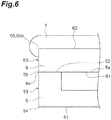
- FIG. 6 is a cross-sectional view taken along line VI-VI in FIG. 5 .
- FIG. 7 is a cross-sectional view taken along line VII-VII in FIG. 5 .
- the intraoral sensor 1 includes a main body portion 2 and a wiring cable 3.
- the main body portion 2 includes a detection surface 21.
- the wiring cable 3 is fixed to the main body portion 2 and is electrically connected to the main body portion 2.
- the wiring cable 3 is detachably fixed to a side opposite to the detection surface 21 in the main body portion 2.
- the main body portion 2 includes a detection surface 21. As illustrated in FIG. 4 , the main body portion 2 includes a support substrate 4, an image sensor 5, a fiber optical plate (FOP) 6, a scintillator 7, a wiring substrate 11, an IC 12, a connector 13, a case 8, and a buffer material 9.
- FOP fiber optical plate
- the support substrate 4 has a polygonal plate shape.
- the support substrate 4 includes a first main surface 41, a second main surface 42, and a plurality of lateral surfaces 43.
- the first main surface 41 has a polygonal shape.
- the second main surface 42 has a polygonal shape.
- the second main surface 42 has a hexagonal shape.
- the support substrate 4 includes six lateral surfaces 43.
- the wiring substrate 11 is disposed on the first main surface 41.
- the IC 12 and the connector 13 are disposed on the wiring substrate 11.
- a wire and the image sensor 5 are disposed on the second main surface 42.
- the wire is a circuit of an A/D converter.
- the FOP 6 is disposed on the image sensor 5.
- the scintillator 7 is disposed on the FOP 6.
- a material of the support substrate 4 is glass or Si.
- the image sensor 5 is a CMOS image sensor.
- the image sensor 5 has a polygonal plate shape.
- the image sensor 5 includes a first main surface 51, a second main surface 52, and a plurality of lateral surfaces 53.
- the first main surface 51 opposes the support substrate 4.
- the first main surface 51 has a polygonal shape.
- the second main surface 52 opposes the FOP 6.
- the second main surface 52 has a polygonal shape.
- the second main surface 52 has a hexagonal shape.
- the image sensor 5 includes six lateral surfaces 53.
- Each of the lateral surfaces 53 connects the edge 54 of the first main surface 51 and the edge 55 of the second main surface 52.
- the lateral surfaces 53 adjacent to each other constitute a plurality of ridge portions 53a.
- the image sensor 5 includes six ridge portions 53a.
- a width of the image sensor 5 in the X-axis direction orthogonal to the Z-axis is 33.92 mm.
- a width of the image sensor 5 in a Y-axis direction orthogonal to the Z-axis and the X-axis is 21.6 mm.
- the thickness of the image sensor 5 is several ⁇ m to several tens of ⁇ m.
- the image sensor 5 includes a light detection region 5a.
- the light detection region 5a is constituted by a plurality of pixels.
- the plurality of pixels are two-dimensionally arranged with a predetermined pixel pitch.
- the light detection region 5a has a polygonal shape.
- the light detection region 5a has a hexagonal shape.
- the light detection region 5a is provided on an inner side in comparison to an outer edge of the image sensor 5.
- the light detection region 5a is provided on an inner side in comparison to the edges 54 and 55 of the first main surface 51 and the second main surface 52 of the image sensor 5.
- the light detection region 5a (pixel) is a charge generation region (a photosensitive region) in which charges are generated in response to incident light.
- a width of the light detection region 5a in the X-axis direction is 30 mm.
- a width of the light detection region 5a in the Y-axis direction is 20 mm.
- the image sensor 5 captures an optical image by the light detection region 5a, and outputs an obtained image as an output image signal.
- the image sensor 5 is electrically connected to the wire disposed on the second main surface 42 of the support substrate 4 by a wire 14.
- the FOP 6 covers the light detection region 5a of the image sensor 5.
- the FOP 6 includes a plurality of optical fibers.
- the plurality of optical fibers are two-dimensionally arranged with a predetermined arrangement pitch, and are bundled.
- the FOP 6 transmits the optical image by the plurality of optical fibers which are bundled.
- the FOP 6 includes an input end surface and an output end surface.
- the input end surface is constituted by an end surface on one side of the plurality of optical fibers.
- the output end surface is constituted by an end surface on the other side of the plurality of optical fibers.
- the FOP 6 transmits an optical image that is input from the input end surface and becomes an image capturing target to the output end surface.
- the FOP 6 has a polygonal plate shape.
- the FOP 6 includes a first main surface 61, a second main surface 62, and a plurality of lateral surfaces 63.
- the first main surface 61 opposes the image sensor 5.
- the first main surface 61 has a polygonal shape.
- the second main surface 62 opposes the scintillator 7.
- the second main surface 62 has a polygonal shape.
- the second main surface 62 has a hexagonal shape.
- the FOP 6 includes six lateral surfaces 63.
- the edge 65 of the second main surface 62 is constituted by a plurality of corner portions 65a and a plurality of side portions 65b. Each of the plurality of side portions 65b connects the corner portions 65a adjacent to each other.
- the corner portions 65a are parts of the edge 65 of the second main surface 62.
- the corner portion 65a is linear segment having a predetermined length from the vertex of an angle of the edge 65 of the second main surface 62. For example, a length of the corner portions 65a is 0.9 mm.
- Each of the lateral surfaces 63 connects the edge 64 of the first main surface 61 and the edge 65 of the second main surface 62.
- the lateral surfaces 63 adjacent to each other constitute a plurality of ridge portions 63a.
- the edge 65 includes six corner portions 65a and six side portions 65b.
- the FOP 6 includes six ridge portions 63a.
- a width of the FOP 6 in the X-axis direction is 33 mm.
- a width of the FOP 6 in the Y-axis direction is 21.8 mm.
- the thickness of the FOP 6 is 1.5 mm.
- the lateral surfaces 63 of the FOP 6 on the wiring cable 3 side in the X-axis direction are provided on an inner side in comparison to the lateral surfaces 53 of the image sensor 5 when viewed from the Z-axis direction.
- the other lateral surfaces 63 of the FOP 6 overlap the other lateral surfaces 53 of the image sensor 5 when viewed from the Z-axis direction.
- the scintillator 7 is provided on the second main surface 62 and the plurality of lateral surfaces 63 of the FOP 6 to cover the light detection region 5a of the image sensor 5.
- the scintillator 7 spreads on the second main surface 62 of the FOP 6 and reaches the plurality of lateral surfaces 63 through the edge 65 of the second main surface 62.
- the scintillator 7 emits fluorescence (scintillation light) in accordance with incidence of radiation.
- the scintillator 7 reaches the lateral surfaces 63 from the second main surface 62 of the FOP 6 through the side portions 65b.
- the scintillator 7 is not provided in the respective corner portions 65a of the FOP 6.
- the scintillator 7 is provided on an inner side in comparison to to the corner portions 65a on the second main surface 62 of the FOP 6.
- the scintillator 7 is not provided in a region 65c that is sandwiched by the corner portions 65a in the second main surface 62 of the FOP 6.
- the region 65c sandwiched by the corner portions 65a in the second main surface 62 of the FOP 6 is exposed.
- the scintillator 7 is not provided in the ridge portions 63a of the FOP 6.
- the scintillator 7 does not reach the ridge portions 63a on the lateral surfaces 63 of the FOP 6.
- the scintillator 7 is not provided in a region within a predetermined range from the ridge portions 63a on the lateral surfaces 63 of the FOP 6.
- the region within the predetermined range from the ridge portions 63a on the lateral surfaces 63 of the FOP 6 is exposed.
- the region within the predetermined range from the ridge portions 63a on the lateral surfaces 63 of the FOP 6 is a range up to a distance that is equal to a length of the corner portions 65a from the ridge portions 63a.
- the scintillator 7 is provided on the second main surface 62 and the plurality of lateral surfaces 63 of the FOP 6 in such a manner that the respective corner portions 65a and the respective ridge portions 63a of the FOP 6 are exposed.
- the thickness of the scintillator 7 is 100 ⁇ m.
- the scintillator 7 is formed from a scintillator material.
- the scintillator material contains cesium iodide (CsI) such as CsI:Tl or CsI:Na as a main component.
- CsI has a structure in which a plurality of needle shaped crystals (columnar crystals) are forested.
- the wiring substrate 11 is disposed on the first main surface 41 of the support substrate 4.
- the wiring substrate 11 is a printed substrate in which an electrode, a wire, and the like are disposed on a front surface.
- the electrode or the wire which is disposed on the front surface of the wiring substrate 11 is electrically connected to the wire disposed on the support substrate 4. That is, the electrode or the wire which is disposed on the wiring substrate 11 is electrically connected to the image sensor 5.
- the wiring substrate 11 has a polygonal plate shape. When viewed from the Z-axis direction, respective lateral surfaces of the wiring substrate 11 overlap the lateral surfaces 43 of the support substrate 4. For example, the thickness of the wiring substrate 11 is 1 mm.
- the IC 12 is disposed on the wiring substrate 11.
- the IC 12 is electrically connected to the image sensor 5 through the electrode or the wire which is disposed on the wiring substrate 11.
- the connector 13 is disposed on the wiring substrate 11. The connector 13 is electrically connected to the IC 12.
- the case 8 contains the support substrate 4, the image sensor 5, the FOP 6, the scintillator 7, the wiring substrate 11, the IC 12, and the connector 13.
- An internal space of the case 8 is formed along to an outer edge of a structure including the image sensor 5, the FOP 6, and the scintillator 7 when viewed from the Z-axis direction.
- the case 8 includes a first case 81 and a second case 82.
- a fixing portion 83 that fixes the wiring cable 3 is provided in the first case 81.
- the first case 81 and the second case 82 are engaged with each other. Examples of a material of the case 8 is ABS resin having impact resistance, or the like.
- the buffer material 9 is disposed between the structure and the case 8.
- the structure includes the image sensor 5, the FOP 6, and the scintillator 7.
- the buffer material 9 is in contact with the structure.
- the buffer material 9 is disposed at least between a side of the structure which is opposite to a lead-out direction of the wiring cable 3 in the X-axis direction, and the case 8.
- a gap for example, a gap of 500 ⁇ m
- the buffer material 9 is disposed is provided between the side of the structure which is opposite to the lead-out direction of the wiring cable 3 in the X-axis direction, and the case 8.
- the buffer material 9 may be disposed over the entire periphery of the structure including the image sensor 5, the FOP 6, and the scintillator 7 when viewed from the Z-axis direction.
- a gap for example, a gap of 200 ⁇ m
- a material of the buffer material 9 is silicone rubber or the like.
- the wiring cable 3 is fixed to the fixing portion 83 of the case 8.
- the wiring cable 3 is electrically connected to the connector 13.
- the wiring cable 3 is a USB cable, and connects the main body portion 2, for example, to a PC.
- the wiring cable 3 is detachably fixed to the fixing portion 83.
- the intraoral sensor 1 configured as described above is inserted into an oral cavity of a patient, and is disposed in such a manner that the detection surface 21 of the main body portion 2 opposes a radiation source disposed at the outside of the oral cavity through teeth or gums.
- a radiation source disposed at the outside of the oral cavity through teeth or gums.
- the scintillator 7 emits fluorescence in correspondence with the intensity of the incident radiation.
- the fluorescence is transferred to the light detection region 5a of the image sensor 5 by the FOP 6, and is converted into an electric signal in the image sensor 5.
- the electric signal converted in the image sensor 5 is transmitted to a PC through the wire 14, the support substrate 4, the wiring substrate 11, the wiring cable 3, and the like.
- the electric signal is converted into a fluoroscopic image of the teeth or the gums in the PC.
- the scintillator 7 is provided on the second main surface 62 and the plurality of lateral surfaces 63 in such a manner that the corner portions 65a and the ridge portions 63 a of the FOP 6 are exposed. That is, the scintillator 7 is not located on the corner portions 65a and the ridge portions 63a of the FOP 6. Accordingly, even in a case where the intraoral sensor 1 receives impact from the outside, the impact is less likely to be transferred to the scintillator 7, and thus the scintillator 7 is less likely to be peeled off.
- the scintillator 7 As in the intraoral sensor 1, in a case where the scintillator 7 is provided also in the lateral surfaces 63 of the FOP 6, impact from the outside of the intraoral sensor 1 is likely to be transferred to the scintillator 7. According to this, the scintillator 7 is likely to be peeled off from the corner portions 65a and the ridge portions 63a of the FOP 6. In the intraoral sensor 1, as described above, since the scintillator 7 is not located on the corner portions 65a and the ridge portions 63a of the FOP 6, the scintillator 7 is less likely to be peeled off from the FOP 6. That is, in a case where the scintillator 7 is also provided on the lateral surfaces 63 of the FOP 6, the above-described effect in which the scintillator 7 is less likely to be peeled off becomes particularly remarkable.
- the scintillator 7 is formed from the scintillator material that contains CsI as a main component.
- the scintillator 7 can be formed by vapor deposition, and thus it is possible to easily provide the scintillator 7.
- CsI has a structure in which a plurality of needle shaped crystals are forested. Light emitted by the needle shaped crystals is less likely to spread to the periphery in comparison to granular crystals. According to this, light emitted by the needle shaped crystals is more accurately transferred to positions of the image sensor 5 which corresponding to the needle shaped crystals. Accordingly, it is possible to improve resolution of an image of the image sensor 5.
- the buffer material 9 is disposed between the structure and the case 8.
- the structure includes the image sensor 5, the FOP 6, and the scintillator 7. According to this configuration, impact which the intraoral sensor 1 receives from the outside is less likely to be transferred to the scintillator 7. Accordingly, peeling-off of the scintillator 7 is more reliably suppressed.
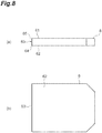
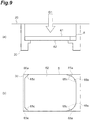
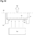
- FIG. 8 to FIG. 11 are views illustrating the method for manufacturing the intraoral sensor 1.
- FIG. 8 and FIG. 9 are views illustrating the method for manufacturing the intraoral sensor 1.
- FIG. 8 and FIG. 9 are views illustrating the method for manufacturing the intraoral sensor 1.
- FIG. 8 and FIG. 9 are views illustrating the method for manufacturing the intraoral sensor 1.
- FIG. 8 and FIG. 9 are views illustrating the method for manufacturing the intraoral sensor 1.
- FIG. 8 first, FOP 6 is prepared.
- the FOP 6 is placed on a jig 30 that is disposed inside a chamber 20 along a direction D1.
- the jig 30 has a shape that covers the respective corner portions 65a of the FOP 6.
- the jig 30 has a shape that covers the regions 65c sandwiched by the corner portions 65a in the second main surface 62 of the FOP 6.
- the scintillator 7 is provided. Specifically, the scintillator 7 is provided on the second main surface 62 and the plurality of lateral surfaces 63 in such a manner that the corner portions 65a and the ridge portions 63a of the FOP 6 are exposed.
- the plurality of corner portions 65a are covered with the jig 30 that supports the FOP 6.
- the scintillator material that constitutes the scintillator 7 is vapor deposited with the jig 30 as a mask. At this time, the scintillator 7 is also vapor deposited on the lateral surfaces 63 which constitute the side portions 65b of the FOP 6.
- the scintillator material contains CsI as a main component.
- the FOP 6 is peeled off from the jig 30 along a direction D2. As a result, as illustrated in FIG. 11 , the FOP 6 on which the scintillator 7 is vapor deposited is obtained.
- the FOP 6 on which the scintillator 7 is vapor deposited is disposed on the image sensor 5 that is disposed on the support substrate 4.
- the support substrate 4 is a substrate that supports the image sensor 5 in a process of manufacturing the image sensor 5.
- the support substrate 4, the image sensor 5, the FOP 6, and the scintillator 7 are contained in a first case 81 of the case 8.
- the wiring substrate 11 on which the IC 12 and the connector 13 are disposed are contained in the first case 81 in advance.
- the support substrate 4 and the wiring substrate 11 are fixed.
- the wire disposed on the support substrate 4, and the electrode or the wire that is disposed on the wiring substrate 11 are electrically connected to each other.
- the wire disposed on the support substrate 4 and the image sensor 5 are electrically connected by the wire 14.
- a second case 82 engages with the first case 81.
- the wiring cable 3 is mounted and fixed to the fixing portion 83 of the case 8, and is electrically connected to the connector 13.
- the scintillator 7 is provided on the second main surface 62 and the plurality of lateral surfaces 63 in such a manner that the corner portions 65a and the ridge portions 63a of the FOP 6 are exposed. Accordingly, as described above, the intraoral sensor 1 in which an increase in size is suppressed and reliability is improved is obtained.
- the plurality of corner portions 65a are covered with the jig 30 that support the FOP 6, and the scintillator material that constitutes the scintillator 7 is vapor deposited with the jig 30 as a mask. In this case, it is not necessary to additionally prepare a mask that covers the plurality of corner portions 65a. Accordingly, the process of manufacturing the intraoral sensor 1 is simplified.
- the scintillator material contains CsI as a main component. In this case, formation of the scintillator 7 by the vapor deposition becomes simple.
- the intraoral sensor 1 may include a radio communication device (not illustrated) instead of the wiring cable 3. In this case, the intraoral sensor 1 transmits an electric signal from the image sensor 5 to the outside by the radio communication device.
- the first main surface 61 and the second main surface 62 of the FOP 6 may not have the hexagonal shape.
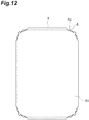
- the first main surface 61 and the second main surface 62 of the FOP 6 only have to have a polygonal shape. As illustrated in FIG. 12 , for example, the first main surface 61 and the second main surface 62 of the FOP 6 may have an octagonal shape.
- the first main surface 51 and the second main surface 52 of the image sensor 5 may not have the hexagonal shape.
- the first main surface 51 and the second main surface 52 of the image sensor 5 may have a polygonal shape.
- the first main surface 51 and the second main surface 52 of the image sensor 5 may have an octagonal shape.
- the first main surface 41 and the second main surface 42 of the support substrate 4 may not have the hexagonal shape.
- the first main surface 41 and the second main surface 42 of the support substrate 4 may have a polygonal shape.
- the first main surface 41 and the second main surface 42 of the support substrate 4 may have an octagonal shape.
- the scintillator 7 may not be provided in the entirety of a region except for the ridge portions 63a in the lateral surfaces 63 of the FOP 6.
- the scintillator 7 may not be provided in a part of the region except for ridge portions 63a in the lateral surfaces 63 of the FOP 6.
- a part of the region except for the ridge portions 63a in the lateral surfaces 63 of the FOP 6 may be exposed.
- the jig 30 may cover a part of the corner portions 65a and a part of the side portions 65b of the FOP 6, and may support the FOP 6.
- the other corner portions 65a of the FOP 6 only have to be covered with a mask 40.
- a position of the part of the side portion 65b which is covered with and is supported by the jig 30 can be set to various positions on the side portions 65b.
- the part of the side portion 65b may be located on any side portion 65b out of the side portions 65b between the corner portions 65a adjacent to each other.
Landscapes
- Health & Medical Sciences (AREA)
- Life Sciences & Earth Sciences (AREA)
- Engineering & Computer Science (AREA)
- Physics & Mathematics (AREA)
- Medical Informatics (AREA)
- Molecular Biology (AREA)
- High Energy & Nuclear Physics (AREA)
- Surgery (AREA)
- General Health & Medical Sciences (AREA)
- Biomedical Technology (AREA)
- Nuclear Medicine, Radiotherapy & Molecular Imaging (AREA)
- Optics & Photonics (AREA)
- Pathology (AREA)
- Veterinary Medicine (AREA)
- Biophysics (AREA)
- Heart & Thoracic Surgery (AREA)
- Public Health (AREA)
- Animal Behavior & Ethology (AREA)
- Radiology & Medical Imaging (AREA)
- Oral & Maxillofacial Surgery (AREA)
- Dentistry (AREA)
- Spectroscopy & Molecular Physics (AREA)
- General Physics & Mathematics (AREA)
- Audiology, Speech & Language Pathology (AREA)
- Measurement Of Radiation (AREA)
- Apparatus For Radiation Diagnosis (AREA)
- Endoscopes (AREA)
Abstract
Description
- The present invention relates to an intraoral sensor and a method for manufacturing an intraoral sensor.
- Known intraoral sensors include an image sensor, a fiber optical plate, a scintillator, and a case (for example, refer to Patent Literature 1). The case containing the image sensor, the fiber optical plate, and the scintillator. The scintillator is disposed on the fiber optical plate.
- Patent Literature 1:
US Patent No. 9,357,972 - In the intraoral sensor, typically, the fiber optical plate has a polygonal shape in a plan view. An outer edge of the fiber optical plate and an outer edge of the scintillator match each other when viewed from a direction orthogonal to the fiber optical plate. In a case where impact is applied to the intraoral sensor from the outside, the impact is transferred to the scintillator through the case. In this case, there is a concern that in the scintillator, a portion located on a corner of the fiber optical plate may be peeled off from the fiber optical plate. When the scintillator is peeled off from the fiber optical plate, reliability of the intraoral sensor deteriorates.
- In the intraoral sensor disclosed in
Patent Literature 1, the shape of the case is set in such a manner that a gap between the case and the fiber optical plate is enlarged at a position corresponding to a corner portion of the fiber optical plate. Accordingly, impact from the outside is less likely to be transferred to the scintillator. However, in a case where the shape of the case is set as described above, an external shape of the case is large, and thus it is difficult to avoid an increase in size of the intraoral sensor. - An object of a first aspect of the invention is to provide an intraoral sensor in which an improvement of reliability and suppression of an increase in size are compatible. An object of a second aspect of the invention is to provide a method for manufacturing the intraoral sensor in which the improvement of the reliability and the suppression of the increase in size are compatible.
- A first aspect of the invention, provides an intraoral sensor including: an image sensor including a light detection region; a fiber optical plate; a scintillator; and a case. The fiber optical plate is disposed on the image sensor to cover the light detection region. The scintillator is disposed on the fiber optical plate. The case contains the image sensor, the fiber optical plate, and the scintillator. The fiber optical plate includes a first main surface, a second main surface, and a plurality of lateral surfaces. The first main surface opposes the image sensor, and has a polygonal shape. The second main surface has a polygonal shape. The plurality of lateral surfaces connect an edge of the first main surface and an edge of the second main surface. The second main surface opposes the scintillator. The edge of the second main surface is constituted by a plurality of corner portions and a plurality of side portions. The plurality of side portions connect the corner portions adjacent to each other. The scintillator is provided on the second main surface and the plurality of lateral surfaces in such a manner that the corner portions and the ridge portions constituted by the lateral surfaces adjacent to each other are exposed.
- In the first aspect, the scintillator is provided on the second main surface and the plurality of lateral surfaces in such a manner that the corner portions and the ridge portions of the fiber optical plate are exposed. That is, the scintillator is not located on the corner portions and the ridge portions of the fiber optical plate. Accordingly, even in a case where the intraoral sensor receives impact from the outside, the impact is less likely to be transferred to the scintillator, and thus the scintillator is less likely to be peeled off. As a result, in the first aspect, it is not necessary to enlarge an external shape of the case to suppress peeling-off of the scintillator, and thus an increase in size of the intraoral sensor is suppressed. As described above, the scintillator is less likely to be peeled off. As a result, in the first aspect, reliability of the intraoral sensor is improved.
- In the first aspect, the scintillator may be formed from a scintillator material containing CsI as a main component. In this case, the scintillator can be formed by vapor deposition, and thus it is possible to easily provide the scintillator.
- The first aspect may further include a buffer material. In this case, the buffer material is disposed between a structure and the case and contacting with the structure. The structure includes the image sensor, the fiber optical plate, and the scintillator. According to this configuration, impact which the intraoral sensor receives from the outside is less likely to be transferred to the scintillator. Accordingly, peeling-off of the scintillator is more reliably suppressed.
- A second aspect of the invention provides a method for manufacturing an intraoral sensor. The intraoral sensor includes a structure including an image sensor, a fiber optical plate, and a scintillator, and a case containing the structure. In the second aspect, the fiber optical plate including a first main surface, a second main surface, and a plurality of lateral surfaces is prepared, and the scintillator is provided on the second main surface and the plurality of lateral surfaces. The first main surface has a polygonal shape. The second main surface is opposite to the first main surface and has a polygonal shape. The plurality of lateral surfaces connect an edge of the first main surface and an edge of the second main surface. The edge of the second main surface is constituted by a plurality of corner portions, and a plurality of side portions connecting the corner portions adjacent to each other. When providing the scintillator on the second main surface and the plurality of lateral surfaces, the corner portions, and the ridge portions constituted by the lateral surfaces adjacent to each other are exposed.
- In the second aspect, the scintillator is provided on the second main surface and the plurality of lateral surfaces in such a manner that the corner portions and the ridge portions of the fiber optical plate are exposed. Accordingly, as described above, the intraoral sensor in which an increase in size is suppressed and reliability is improved is obtained.
- In the second aspect, when providing the scintillator, may caver the plurality of corner portions with a jig supporting the fiber optical plate, and vapor depositing a scintillator material constituting the scintillator with the jig as a mask. In this case, it is not necessary to additionally provide a mask that covers the plurality of corner portions. Accordingly, the process of manufacturing the intraoral sensor is simplified.
- In the second aspect, the scintillator material may contain CsI as a main component. In this case, formation of the scintillator by vapor deposition becomes simple.
- According to the first aspect of the invention, an intraoral sensor in which an improvement of reliability and suppression of an increase in size are compatible is provided. According to the second aspect of the invention, a method for manufacturing the intraoral sensor in which the improvement of the reliability and the suppression of the increase in size are compatible is provided.
-
-
FIG. 1 is a plan view of an intraoral sensor according to an embodiment. -
FIG. 2 is a front view of the intraoral sensor. -
FIG. 3 is a bottom view of the intraoral sensor. -
FIG. 4 is a cross-sectional view taken along line IV-IV inFIG. 3 . -
FIG. 5 is a view illustrating an internal structure of the intraoral sensor. -
FIG. 6 is a cross-sectional view taken along line VI-VI inFIG. 5 . -
FIG. 7 is a cross-sectional view taken along line VII-VII inFIG. 5 . -
FIG. 8 is a view illustrating a method for manufacturing the intraoral sensor. -
FIG. 9 is a view illustrating the method for manufacturing the intraoral sensor. -
FIG. 10 is a view illustrating the method for manufacturing the intraoral sensor. -
FIG. 11 is a view illustrating the method for manufacturing the intraoral sensor. -
FIG. 12 is a view illustrating a modification example of the intraoral sensor. -
FIG. 13 is a view illustrating a modification example of the method for manufacturing the intraoral sensor. - Hereinafter, an embodiment of the invention will be described in detail with reference to the accompanying drawings. In description, the same reference numeral will be given to the same element or an element having the same function, and redundant description will be omitted.
- A configuration of an
intraoral sensor 1 according to this embodiment will be described with reference toFIG. 1 to FIG. 7 .FIG 1 is a plan view of theintraoral sensor 1 according to this embodiment.FIG. 2 is a front view of theintraoral sensor 1.FIG 3 is a bottom view of theintraoral sensor 1.FIG. 4 is a cross-sectional view taken along line IV-IV inFIG. 3 .FIG. 5 is a view illustrating an internal structure of theintraoral sensor 1.FIG. 6 is a cross-sectional view taken along line VI-VI inFIG. 5 .FIG. 7 is a cross-sectional view taken along line VII-VII inFIG. 5 . - As illustrated in
FIG. 1 to FIG. 3 , theintraoral sensor 1 includes amain body portion 2 and awiring cable 3. Themain body portion 2 includes adetection surface 21. Thewiring cable 3 is fixed to themain body portion 2 and is electrically connected to themain body portion 2. Thewiring cable 3 is detachably fixed to a side opposite to thedetection surface 21 in themain body portion 2. - The
main body portion 2 includes adetection surface 21. As illustrated inFIG. 4 , themain body portion 2 includes asupport substrate 4, animage sensor 5, a fiber optical plate (FOP) 6, ascintillator 7, awiring substrate 11, anIC 12, aconnector 13, acase 8, and abuffer material 9. - As illustrated in
FIG. 4 andFIG. 5 , thesupport substrate 4 has a polygonal plate shape. Thesupport substrate 4 includes a firstmain surface 41, a secondmain surface 42, and a plurality of lateral surfaces 43. The firstmain surface 41 has a polygonal shape. For example, the firstmain surface 41 has a hexagonal shape. The secondmain surface 42 has a polygonal shape. For example, the secondmain surface 42 has a hexagonal shape. In this embodiment, thesupport substrate 4 includes sixlateral surfaces 43. - The
wiring substrate 11 is disposed on the firstmain surface 41. TheIC 12 and theconnector 13 are disposed on thewiring substrate 11. A wire and theimage sensor 5 are disposed on the secondmain surface 42. For example, the wire is a circuit of an A/D converter. TheFOP 6 is disposed on theimage sensor 5. Thescintillator 7 is disposed on theFOP 6. For example, a material of thesupport substrate 4 is glass or Si. - The
image sensor 5 is a CMOS image sensor. Theimage sensor 5 has a polygonal plate shape. Theimage sensor 5 includes a firstmain surface 51, a secondmain surface 52, and a plurality of lateral surfaces 53. The firstmain surface 51 opposes thesupport substrate 4. The firstmain surface 51 has a polygonal shape. For example, the firstmain surface 51 has a hexagonal shape. The secondmain surface 52 opposes theFOP 6. The secondmain surface 52 has a polygonal shape. For example, the secondmain surface 52 has a hexagonal shape. In this embodiment, theimage sensor 5 includes sixlateral surfaces 53. - An
edge 54 of the firstmain surface 51 and anedge 55 of the secondmain surface 52 overlap each other when viewed from the Z-axis direction that is a direction orthogonal to the firstmain surface 51 and the secondmain surface 52. Each of the lateral surfaces 53 connects theedge 54 of the firstmain surface 51 and theedge 55 of the secondmain surface 52. The lateral surfaces 53 adjacent to each other constitute a plurality ofridge portions 53a. In this embodiment, theimage sensor 5 includes sixridge portions 53a. - For example, a width of the
image sensor 5 in the X-axis direction orthogonal to the Z-axis is 33.92 mm. For example, a width of theimage sensor 5 in a Y-axis direction orthogonal to the Z-axis and the X-axis is 21.6 mm. For example, the thickness of theimage sensor 5 is several µm to several tens of µm. When viewed from the Z-axis direction, thelateral surface 53 of theimage sensor 5 on awiring cable 3 side in the X-axis direction is provided on an inner side in comparison to thelateral surface 43 of thesupport substrate 4. When viewed from the Z-axis direction, anotherlateral surface 53 of theimage sensor 5 overlap anotherlateral surface 43 of thesupport substrate 4. - The
image sensor 5 includes alight detection region 5a. Thelight detection region 5a is constituted by a plurality of pixels. The plurality of pixels are two-dimensionally arranged with a predetermined pixel pitch. Thelight detection region 5a has a polygonal shape. For example, thelight detection region 5a has a hexagonal shape. When viewed from the Z-axis direction, thelight detection region 5a is provided on an inner side in comparison to an outer edge of theimage sensor 5. When viewed from the Z-axis direction, thelight detection region 5a is provided on an inner side in comparison to theedges main surface 51 and the secondmain surface 52 of theimage sensor 5. Thelight detection region 5a (pixel) is a charge generation region (a photosensitive region) in which charges are generated in response to incident light. - For example, a width of the
light detection region 5a in the X-axis direction is 30 mm. For example, a width of thelight detection region 5a in the Y-axis direction is 20 mm. Theimage sensor 5 captures an optical image by thelight detection region 5a, and outputs an obtained image as an output image signal. Theimage sensor 5 is electrically connected to the wire disposed on the secondmain surface 42 of thesupport substrate 4 by awire 14. - The
FOP 6 covers thelight detection region 5a of theimage sensor 5. TheFOP 6 includes a plurality of optical fibers. The plurality of optical fibers are two-dimensionally arranged with a predetermined arrangement pitch, and are bundled. TheFOP 6 transmits the optical image by the plurality of optical fibers which are bundled. TheFOP 6 includes an input end surface and an output end surface. The input end surface is constituted by an end surface on one side of the plurality of optical fibers. The output end surface is constituted by an end surface on the other side of the plurality of optical fibers. TheFOP 6 transmits an optical image that is input from the input end surface and becomes an image capturing target to the output end surface. - The
FOP 6 has a polygonal plate shape. TheFOP 6 includes a firstmain surface 61, a secondmain surface 62, and a plurality of lateral surfaces 63. The firstmain surface 61 opposes theimage sensor 5. The firstmain surface 61 has a polygonal shape. For example, the firstmain surface 61 has a hexagonal shape. The secondmain surface 62 opposes thescintillator 7. The secondmain surface 62 has a polygonal shape. For example, the secondmain surface 62 has a hexagonal shape. In this embodiment, theFOP 6 includes sixlateral surfaces 63. - An
edge 64 of the firstmain surface 61 and anedge 65 of the secondmain surface 62 overlap each other when viewed from the Z-axis direction. Theedge 65 of the secondmain surface 62 is constituted by a plurality ofcorner portions 65a and a plurality ofside portions 65b. Each of the plurality ofside portions 65b connects thecorner portions 65a adjacent to each other. Thecorner portions 65a are parts of theedge 65 of the secondmain surface 62. Thecorner portion 65a is linear segment having a predetermined length from the vertex of an angle of theedge 65 of the secondmain surface 62. For example, a length of thecorner portions 65a is 0.9 mm. Each of the lateral surfaces 63 connects theedge 64 of the firstmain surface 61 and theedge 65 of the secondmain surface 62. The lateral surfaces 63 adjacent to each other constitute a plurality ofridge portions 63a. In this embodiment, theedge 65 includes sixcorner portions 65a and sixside portions 65b. In this embodiment, theFOP 6 includes sixridge portions 63a. - For example, a width of the
FOP 6 in the X-axis direction is 33 mm. For example, a width of theFOP 6 in the Y-axis direction is 21.8 mm. For example, the thickness of theFOP 6 is 1.5 mm. The lateral surfaces 63 of theFOP 6 on thewiring cable 3 side in the X-axis direction are provided on an inner side in comparison to the lateral surfaces 53 of theimage sensor 5 when viewed from the Z-axis direction. The otherlateral surfaces 63 of theFOP 6 overlap the otherlateral surfaces 53 of theimage sensor 5 when viewed from the Z-axis direction. - The
scintillator 7 is provided on the secondmain surface 62 and the plurality oflateral surfaces 63 of theFOP 6 to cover thelight detection region 5a of theimage sensor 5. Thescintillator 7 spreads on the secondmain surface 62 of theFOP 6 and reaches the plurality oflateral surfaces 63 through theedge 65 of the secondmain surface 62. Thescintillator 7 emits fluorescence (scintillation light) in accordance with incidence of radiation. - As illustrated in
FIG. 5 andFIG. 6 , thescintillator 7 reaches the lateral surfaces 63 from the secondmain surface 62 of theFOP 6 through theside portions 65b. Thescintillator 7 is not provided in therespective corner portions 65a of theFOP 6. As illustrated inFIG. 5 andFIG. 7 , thescintillator 7 is provided on an inner side in comparison to to thecorner portions 65a on the secondmain surface 62 of theFOP 6. Thescintillator 7 is not provided in aregion 65c that is sandwiched by thecorner portions 65a in the secondmain surface 62 of theFOP 6. Theregion 65c sandwiched by thecorner portions 65a in the secondmain surface 62 of theFOP 6 is exposed. - The
scintillator 7 is not provided in theridge portions 63a of theFOP 6. Thescintillator 7 does not reach theridge portions 63a on the lateral surfaces 63 of theFOP 6. Thescintillator 7 is not provided in a region within a predetermined range from theridge portions 63a on the lateral surfaces 63 of theFOP 6. The region within the predetermined range from theridge portions 63a on the lateral surfaces 63 of theFOP 6 is exposed. For example, the region within the predetermined range from theridge portions 63a on the lateral surfaces 63 of theFOP 6 is a range up to a distance that is equal to a length of thecorner portions 65a from theridge portions 63a. - As described above, the
scintillator 7 is provided on the secondmain surface 62 and the plurality oflateral surfaces 63 of theFOP 6 in such a manner that therespective corner portions 65a and therespective ridge portions 63a of theFOP 6 are exposed. For example, the thickness of thescintillator 7 is 100 µm. Thescintillator 7 is formed from a scintillator material. The scintillator material contains cesium iodide (CsI) such as CsI:Tl or CsI:Na as a main component. CsI has a structure in which a plurality of needle shaped crystals (columnar crystals) are forested. - Description will be given with reference to
FIG. 4 andFIG. 5 again. Thewiring substrate 11 is disposed on the firstmain surface 41 of thesupport substrate 4. Thewiring substrate 11 is a printed substrate in which an electrode, a wire, and the like are disposed on a front surface. The electrode or the wire which is disposed on the front surface of thewiring substrate 11 is electrically connected to the wire disposed on thesupport substrate 4. That is, the electrode or the wire which is disposed on thewiring substrate 11 is electrically connected to theimage sensor 5. - The
wiring substrate 11 has a polygonal plate shape. When viewed from the Z-axis direction, respective lateral surfaces of thewiring substrate 11 overlap the lateral surfaces 43 of thesupport substrate 4. For example, the thickness of thewiring substrate 11 is 1 mm. - The
IC 12 is disposed on thewiring substrate 11. TheIC 12 is electrically connected to theimage sensor 5 through the electrode or the wire which is disposed on thewiring substrate 11. Theconnector 13 is disposed on thewiring substrate 11. Theconnector 13 is electrically connected to theIC 12. - The
case 8 contains thesupport substrate 4, theimage sensor 5, theFOP 6, thescintillator 7, thewiring substrate 11, theIC 12, and theconnector 13. An internal space of thecase 8 is formed along to an outer edge of a structure including theimage sensor 5, theFOP 6, and thescintillator 7 when viewed from the Z-axis direction. - The
case 8 includes afirst case 81 and asecond case 82. A fixingportion 83 that fixes thewiring cable 3 is provided in thefirst case 81. Thefirst case 81 and thesecond case 82 are engaged with each other. Examples of a material of thecase 8 is ABS resin having impact resistance, or the like. - The
buffer material 9 is disposed between the structure and thecase 8. The structure includes theimage sensor 5, theFOP 6, and thescintillator 7. Thebuffer material 9 is in contact with the structure. Thebuffer material 9 is disposed at least between a side of the structure which is opposite to a lead-out direction of thewiring cable 3 in the X-axis direction, and thecase 8. In this case, a gap (for example, a gap of 500 µm) in which thebuffer material 9 is disposed is provided between the side of the structure which is opposite to the lead-out direction of thewiring cable 3 in the X-axis direction, and thecase 8. Thebuffer material 9 may be disposed over the entire periphery of the structure including theimage sensor 5, theFOP 6, and thescintillator 7 when viewed from the Z-axis direction. In this case, a gap (for example, a gap of 200 µm) in which thebuffer material 9 is disposed is further provided between both sides of the structure in the Y-axis direction, and thecase 8. For example, a material of thebuffer material 9 is silicone rubber or the like. - The
wiring cable 3 is fixed to the fixingportion 83 of thecase 8. Thewiring cable 3 is electrically connected to theconnector 13. Thewiring cable 3 is a USB cable, and connects themain body portion 2, for example, to a PC. Thewiring cable 3 is detachably fixed to the fixingportion 83. - The
intraoral sensor 1 configured as described above is inserted into an oral cavity of a patient, and is disposed in such a manner that thedetection surface 21 of themain body portion 2 opposes a radiation source disposed at the outside of the oral cavity through teeth or gums. When radiation is radiated from the radiation source, the radiation is transmitted through the teeth or the gums and is incident to thescintillator 7. Thescintillator 7 emits fluorescence in correspondence with the intensity of the incident radiation. The fluorescence is transferred to thelight detection region 5a of theimage sensor 5 by theFOP 6, and is converted into an electric signal in theimage sensor 5. The electric signal converted in theimage sensor 5 is transmitted to a PC through thewire 14, thesupport substrate 4, thewiring substrate 11, thewiring cable 3, and the like. The electric signal is converted into a fluoroscopic image of the teeth or the gums in the PC. - As described above, in the
intraoral sensor 1, thescintillator 7 is provided on the secondmain surface 62 and the plurality oflateral surfaces 63 in such a manner that thecorner portions 65a and theridge portions 63 a of theFOP 6 are exposed. That is, thescintillator 7 is not located on thecorner portions 65a and theridge portions 63a of theFOP 6. Accordingly, even in a case where theintraoral sensor 1 receives impact from the outside, the impact is less likely to be transferred to thescintillator 7, and thus thescintillator 7 is less likely to be peeled off. As a result, it is not necessary to enlarge an external shape of thecase 8 to suppress peeling-off of thescintillator 7, and thus an increase in size of theintraoral sensor 1 is suppressed. As described above, thescintillator 7 is less likely to be peeled off, and thus reliability of theintraoral sensor 1 is improved. - As in the
intraoral sensor 1, in a case where thescintillator 7 is provided also in the lateral surfaces 63 of theFOP 6, impact from the outside of theintraoral sensor 1 is likely to be transferred to thescintillator 7. According to this, thescintillator 7 is likely to be peeled off from thecorner portions 65a and theridge portions 63a of theFOP 6. In theintraoral sensor 1, as described above, since thescintillator 7 is not located on thecorner portions 65a and theridge portions 63a of theFOP 6, thescintillator 7 is less likely to be peeled off from theFOP 6. That is, in a case where thescintillator 7 is also provided on the lateral surfaces 63 of theFOP 6, the above-described effect in which thescintillator 7 is less likely to be peeled off becomes particularly remarkable. - In the
intraoral sensor 1, thescintillator 7 is formed from the scintillator material that contains CsI as a main component. In this case, thescintillator 7 can be formed by vapor deposition, and thus it is possible to easily provide thescintillator 7. CsI has a structure in which a plurality of needle shaped crystals are forested. Light emitted by the needle shaped crystals is less likely to spread to the periphery in comparison to granular crystals. According to this, light emitted by the needle shaped crystals is more accurately transferred to positions of theimage sensor 5 which corresponding to the needle shaped crystals. Accordingly, it is possible to improve resolution of an image of theimage sensor 5. - In the
intraoral sensor 1, thebuffer material 9 is disposed between the structure and thecase 8. The structure includes theimage sensor 5, theFOP 6, and thescintillator 7. According to this configuration, impact which theintraoral sensor 1 receives from the outside is less likely to be transferred to thescintillator 7. Accordingly, peeling-off of thescintillator 7 is more reliably suppressed. - Next, the method for manufacturing the
intraoral sensor 1 according to this embodiment will be described with reference toFIG. 8 to FIG. 11. FIG. 8 to FIG. 11 are views illustrating the method for manufacturing theintraoral sensor 1. InFIG. 8 andFIG. 9 , (a) is a front view and (b) is a bottom view. As illustrated inFIG. 8 , first,FOP 6 is prepared. Next, as illustrated inFIG. 9 , theFOP 6 is placed on ajig 30 that is disposed inside achamber 20 along a direction D1. Thejig 30 has a shape that covers therespective corner portions 65a of theFOP 6. Thejig 30 has a shape that covers theregions 65c sandwiched by thecorner portions 65a in the secondmain surface 62 of theFOP 6. - Next, as illustrated in
FIG. 10 , thescintillator 7 is provided. Specifically, thescintillator 7 is provided on the secondmain surface 62 and the plurality oflateral surfaces 63 in such a manner that thecorner portions 65a and theridge portions 63a of theFOP 6 are exposed. When providing thescintillator 7, the plurality ofcorner portions 65a are covered with thejig 30 that supports theFOP 6. In addition, the scintillator material that constitutes thescintillator 7 is vapor deposited with thejig 30 as a mask. At this time, thescintillator 7 is also vapor deposited on the lateral surfaces 63 which constitute theside portions 65b of theFOP 6. The scintillator material contains CsI as a main component. Next, theFOP 6 is peeled off from thejig 30 along a direction D2. As a result, as illustrated inFIG. 11 , theFOP 6 on which thescintillator 7 is vapor deposited is obtained. - Next, the
FOP 6 on which thescintillator 7 is vapor deposited is disposed on theimage sensor 5 that is disposed on thesupport substrate 4. Thesupport substrate 4 is a substrate that supports theimage sensor 5 in a process of manufacturing theimage sensor 5. Next, thesupport substrate 4, theimage sensor 5, theFOP 6, and thescintillator 7 are contained in afirst case 81 of thecase 8. At this time, thewiring substrate 11 on which theIC 12 and theconnector 13 are disposed are contained in thefirst case 81 in advance. - Next, the
support substrate 4 and thewiring substrate 11 are fixed. At this process, the wire disposed on thesupport substrate 4, and the electrode or the wire that is disposed on thewiring substrate 11 are electrically connected to each other. Next, the wire disposed on thesupport substrate 4 and theimage sensor 5 are electrically connected by thewire 14. Next, asecond case 82 engages with thefirst case 81. Next, thewiring cable 3 is mounted and fixed to the fixingportion 83 of thecase 8, and is electrically connected to theconnector 13. - As described above, according to the method for manufacturing the
intraoral sensor 1, thescintillator 7 is provided on the secondmain surface 62 and the plurality oflateral surfaces 63 in such a manner that thecorner portions 65a and theridge portions 63a of theFOP 6 are exposed. Accordingly, as described above, theintraoral sensor 1 in which an increase in size is suppressed and reliability is improved is obtained. - In the method for manufacturing the
intraoral sensor 1, when providing thescintillator 7, the plurality ofcorner portions 65a are covered with thejig 30 that support theFOP 6, and the scintillator material that constitutes thescintillator 7 is vapor deposited with thejig 30 as a mask. In this case, it is not necessary to additionally prepare a mask that covers the plurality ofcorner portions 65a. Accordingly, the process of manufacturing theintraoral sensor 1 is simplified. - In the method for manufacturing the
intraoral sensor 1, the scintillator material contains CsI as a main component. In this case, formation of thescintillator 7 by the vapor deposition becomes simple. - Hereinbefore, description has been given of an embodiment of the invention, but the invention is not limited to the above-described embodiment.
- The
intraoral sensor 1 may include a radio communication device (not illustrated) instead of thewiring cable 3. In this case, theintraoral sensor 1 transmits an electric signal from theimage sensor 5 to the outside by the radio communication device. - The first
main surface 61 and the secondmain surface 62 of theFOP 6 may not have the hexagonal shape. The firstmain surface 61 and the secondmain surface 62 of theFOP 6 only have to have a polygonal shape. As illustrated inFIG. 12 , for example, the firstmain surface 61 and the secondmain surface 62 of theFOP 6 may have an octagonal shape. - The first
main surface 51 and the secondmain surface 52 of theimage sensor 5 may not have the hexagonal shape. The firstmain surface 51 and the secondmain surface 52 of theimage sensor 5 may have a polygonal shape. For example, the firstmain surface 51 and the secondmain surface 52 of theimage sensor 5 may have an octagonal shape. - The first
main surface 41 and the secondmain surface 42 of thesupport substrate 4 may not have the hexagonal shape. The firstmain surface 41 and the secondmain surface 42 of thesupport substrate 4 may have a polygonal shape. For example, the firstmain surface 41 and the secondmain surface 42 of thesupport substrate 4 may have an octagonal shape. - The
scintillator 7 may not be provided in the entirety of a region except for theridge portions 63a in the lateral surfaces 63 of theFOP 6. Thescintillator 7 may not be provided in a part of the region except forridge portions 63a in the lateral surfaces 63 of theFOP 6. A part of the region except for theridge portions 63a in the lateral surfaces 63 of theFOP 6 may be exposed. - In the method for manufacturing the
intraoral sensor 1, when providing thescintillator 7, all of thecorner portions 65a may not be covered with thejig 30 that supports theFOP 6. As illustrated inFIG. 13 , thejig 30 may cover a part of thecorner portions 65a and a part of theside portions 65b of theFOP 6, and may support theFOP 6. In this case, theother corner portions 65a of theFOP 6 only have to be covered with amask 40. A position of the part of theside portion 65b which is covered with and is supported by thejig 30 can be set to various positions on theside portions 65b. For example, the part of theside portion 65b may be located on anyside portion 65b out of theside portions 65b between thecorner portions 65a adjacent to each other. - 1: intraoral sensor, 5: image sensor, 5a: light detection region, 6: FOP, 7: scintillator, 8: case, 9: buffer material, 30: jig, 40: mask, 61: first main surface, 62: second main surface, 63: lateral surface, 63a: ridge portion, 64, 65: edge, 65a: corner portion, 65b: side portion.
Claims (6)
- An intraoral sensor comprising:an image sensor including a light detection region;a fiber optical plate is disposed on the image sensor to cover the light detection region;a scintillator is disposed on the fiber optical plate; anda case containing the image sensor, the fiber optical plate, and the scintillator,wherein the fiber optical plate includes,a first main surface opposing the image sensor and having a polygonal shape,a second main surface opposing the scintillator and having a polygonal shape, anda plurality of lateral surfaces connecting an edge of the first main surface and an edge of the second main surface, whereinthe edge of the second main surface includes a plurality of corner portions, and a plurality of side portions connecting the corner portions adjacent to each other, andthe scintillator is provided on the second main surface and the plurality of lateral surfaces in such a manner that the corner portions and the ridge portions constituted by the lateral surfaces adjacent to each other are exposed.
- The intraoral sensor according to claim 1,
wherein the scintillator is formed from a scintillator material containing CsI as a main component. - The intraoral sensor according to claim 1 or 2, further comprising:
a buffer material disposed between a structure and the case, and contacting with the structure, the structure including the image sensor, the fiber optical plate, and the scintillator. - A method for manufacturing an intraoral sensor including a structure including an image sensor, a fiber optical plate, and a scintillator, and a case containing the structure, the method comprising:preparing the fiber optical plate including a first main surface having a polygonal shape, a second main surface opposite to the first main surface and having a polygonal shape, and a plurality of lateral surfaces connecting an edge of the first main surface and an edge of the second main surface, the edge of the second main surface being constituted by a plurality of corner portions and a plurality of side portions connecting the corner portions adjacent to each other; andproviding the scintillator on the second main surface and the plurality of lateral surfaces in such a manner that the corner portions, and the ridge portions constituted by the lateral surfaces adjacent to each other are exposed.
- The method for manufacturing an intraoral sensor according to claim 4,
wherein when providing the scintillator,
covering the plurality of corner portions with a jig supporting the fiber optical plate, and
vapor depositing a scintillator material constituting the scintillator with the jig as a mask. - The method for manufacturing an intraoral sensor according to claim 5,
wherein the scintillator material contains CsI as a main component.
Applications Claiming Priority (2)
| Application Number | Priority Date | Filing Date | Title |
|---|---|---|---|
| JP2017165261A JP6515153B2 (en) | 2017-08-30 | 2017-08-30 | Intraoral sensor and method of manufacturing intraoral sensor |
| PCT/JP2018/031361 WO2019044701A1 (en) | 2017-08-30 | 2018-08-24 | Intraoral sensor and method for producing intraoral sensor |
Publications (3)
| Publication Number | Publication Date |
|---|---|
| EP3677188A1 true EP3677188A1 (en) | 2020-07-08 |
| EP3677188A4 EP3677188A4 (en) | 2021-05-05 |
| EP3677188B1 EP3677188B1 (en) | 2023-06-14 |
Family
ID=65525701
Family Applications (1)
| Application Number | Title | Priority Date | Filing Date |
|---|---|---|---|
| EP18850950.9A Active EP3677188B1 (en) | 2017-08-30 | 2018-08-24 | Intraoral sensor and method for producing intraoral sensor |
Country Status (5)
| Country | Link |
|---|---|
| US (1) | US11576632B2 (en) |
| EP (1) | EP3677188B1 (en) |
| JP (1) | JP6515153B2 (en) |
| KR (1) | KR102554082B1 (en) |
| WO (1) | WO2019044701A1 (en) |
Families Citing this family (4)
| Publication number | Priority date | Publication date | Assignee | Title |
|---|---|---|---|---|
| JP6515152B2 (en) * | 2017-08-30 | 2019-05-15 | 浜松ホトニクス株式会社 | Intraoral sensor and method of manufacturing intraoral sensor |
| JP7046698B2 (en) * | 2018-04-24 | 2022-04-04 | 浜松ホトニクス株式会社 | Radiation detector, manufacturing method of radiation detector, and image processing method |
| USD1064275S1 (en) * | 2021-10-19 | 2025-02-25 | Fairchild Imaging, Inc. | Dental sensor |
| JP2024048855A (en) * | 2022-09-28 | 2024-04-09 | 浜松ホトニクス株式会社 | Intraoral imaging device |
Family Cites Families (9)
| Publication number | Priority date | Publication date | Assignee | Title |
|---|---|---|---|---|
| JPS61225684A (en) * | 1985-03-29 | 1986-10-07 | Hamamatsu Photonics Kk | Scintillation fiber plate and manufacture thereof |
| US5434418A (en) * | 1992-10-16 | 1995-07-18 | Schick; David | Intra-oral sensor for computer aided radiography |
| US5510623A (en) * | 1995-02-24 | 1996-04-23 | Loral Fairchild Corp. | Center readout intra-oral image sensor |
| FR2888043B1 (en) | 2005-07-01 | 2007-11-30 | Atmel Grenoble Soc Par Actions | FIBER OPTICAL IMAGE SENSOR |
| JP5883556B2 (en) * | 2010-06-04 | 2016-03-15 | 浜松ホトニクス株式会社 | Radiation image sensor |
| US8614421B2 (en) * | 2011-03-07 | 2013-12-24 | Teledyne Dalsa Inc. | Method and system for assembly of glass substrate-based radiological imaging sensor |
| WO2012174509A1 (en) * | 2011-06-16 | 2012-12-20 | Suni Medical Imaging, Inc. | X-ray image sensor |
| US9357972B2 (en) * | 2012-07-17 | 2016-06-07 | Cyber Medical Imaging, Inc. | Intraoral radiographic sensors with cables having increased user comfort and methods of using the same |
| JP2014153074A (en) * | 2013-02-05 | 2014-08-25 | Hamamatsu Photonics Kk | Radiation image conversion panel manufacturing method and radiation image conversion panel |
-
2017
- 2017-08-30 JP JP2017165261A patent/JP6515153B2/en active Active
-
2018
- 2018-08-24 KR KR1020207005389A patent/KR102554082B1/en active Active
- 2018-08-24 US US16/641,789 patent/US11576632B2/en active Active
- 2018-08-24 EP EP18850950.9A patent/EP3677188B1/en active Active
- 2018-08-24 WO PCT/JP2018/031361 patent/WO2019044701A1/en not_active Ceased
Also Published As
| Publication number | Publication date |
|---|---|
| WO2019044701A1 (en) | 2019-03-07 |
| KR102554082B1 (en) | 2023-07-12 |
| KR20200046030A (en) | 2020-05-06 |
| EP3677188B1 (en) | 2023-06-14 |
| US11576632B2 (en) | 2023-02-14 |
| JP2019045175A (en) | 2019-03-22 |
| EP3677188A4 (en) | 2021-05-05 |
| US20200261040A1 (en) | 2020-08-20 |
| JP6515153B2 (en) | 2019-05-15 |
Similar Documents
| Publication | Publication Date | Title |
|---|---|---|
| US11576632B2 (en) | Intraoral sensor and method for producing intraoral sensor | |
| US10156641B2 (en) | Radiation image sensing apparatus and radiation image sensing system | |
| US20230038637A1 (en) | Radiation detector, radiation detector manufacturing method, and image processing method | |
| CN107850678B (en) | Detector unit for detector array of radiation imaging modality device | |
| CN105662442B (en) | Radiology Imaging System | |
| US9684083B2 (en) | X-ray detector panel | |
| KR20080114695A (en) | Radiation detector | |
| US11129580B2 (en) | Intraoral sensor and method for producing intraoral sensor | |
| US12253639B2 (en) | Sensor board, radiation imaging apparatus, radiation imaging system, and method of manufacturing sensor board | |
| EP3011907B1 (en) | Production method for radiation detection unit | |
| US20140061485A1 (en) | Radiation imaging apparatus, method for manufacturing the same, and radiation imaging system | |
| US20140367578A1 (en) | X-ray image sensor | |
| JP6373624B2 (en) | Array substrate, radiation detector, and method of manufacturing radiation detector | |
| EP3015051A1 (en) | Imaging unit and endoscope device | |
| JP7206431B2 (en) | Radiation detector, radiation detector manufacturing method, and image processing method | |
| CN111801599A (en) | Radiation detector, radiation imaging apparatus, and manufacturing method of radiation detector | |
| CN121713092A (en) | Radiation imaging apparatus and method of manufacturing radiation imaging apparatus | |
| JP2020079767A (en) | Radiation imaging apparatus and manufacturing method thereof, and radiation imaging system |
Legal Events
| Date | Code | Title | Description |
|---|---|---|---|
| STAA | Information on the status of an ep patent application or granted ep patent |
Free format text: STATUS: THE INTERNATIONAL PUBLICATION HAS BEEN MADE |
|
| PUAI | Public reference made under article 153(3) epc to a published international application that has entered the european phase |
Free format text: ORIGINAL CODE: 0009012 |
|
| STAA | Information on the status of an ep patent application or granted ep patent |
Free format text: STATUS: REQUEST FOR EXAMINATION WAS MADE |
|
| 17P | Request for examination filed |
Effective date: 20200227 |
|
| AK | Designated contracting states |
Kind code of ref document: A1 Designated state(s): AL AT BE BG CH CY CZ DE DK EE ES FI FR GB GR HR HU IE IS IT LI LT LU LV MC MK MT NL NO PL PT RO RS SE SI SK SM TR |
|
| AX | Request for extension of the european patent |
Extension state: BA ME |
|
| DAV | Request for validation of the european patent (deleted) | ||
| DAX | Request for extension of the european patent (deleted) | ||
| A4 | Supplementary search report drawn up and despatched |
Effective date: 20210407 |
|
| RIC1 | Information provided on ipc code assigned before grant |
Ipc: A61B 6/14 20060101AFI20210330BHEP Ipc: A61B 6/00 20060101ALI20210330BHEP Ipc: G01T 1/20 20060101ALI20210330BHEP |
|
| GRAP | Despatch of communication of intention to grant a patent |
Free format text: ORIGINAL CODE: EPIDOSNIGR1 |
|
| STAA | Information on the status of an ep patent application or granted ep patent |
Free format text: STATUS: GRANT OF PATENT IS INTENDED |
|
| INTG | Intention to grant announced |
Effective date: 20230216 |
|
| GRAS | Grant fee paid |
Free format text: ORIGINAL CODE: EPIDOSNIGR3 |
|
| GRAA | (expected) grant |
Free format text: ORIGINAL CODE: 0009210 |
|
| STAA | Information on the status of an ep patent application or granted ep patent |
Free format text: STATUS: THE PATENT HAS BEEN GRANTED |
|
| AK | Designated contracting states |
Kind code of ref document: B1 Designated state(s): AL AT BE BG CH CY CZ DE DK EE ES FI FR GB GR HR HU IE IS IT LI LT LU LV MC MK MT NL NO PL PT RO RS SE SI SK SM TR |
|
| REG | Reference to a national code |
Ref country code: CH Ref legal event code: EP |
|
| REG | Reference to a national code |
Ref country code: DE Ref legal event code: R096 Ref document number: 602018051942 Country of ref document: DE |
|
| REG | Reference to a national code |
Ref country code: AT Ref legal event code: REF Ref document number: 1578632 Country of ref document: AT Kind code of ref document: T Effective date: 20230715 |
|
| P01 | Opt-out of the competence of the unified patent court (upc) registered |
Effective date: 20230630 |
|
| REG | Reference to a national code |
Ref country code: LT Ref legal event code: MG9D |
|
| REG | Reference to a national code |
Ref country code: NL Ref legal event code: MP Effective date: 20230614 |
|
| PG25 | Lapsed in a contracting state [announced via postgrant information from national office to epo] |
Ref country code: SE Free format text: LAPSE BECAUSE OF FAILURE TO SUBMIT A TRANSLATION OF THE DESCRIPTION OR TO PAY THE FEE WITHIN THE PRESCRIBED TIME-LIMIT Effective date: 20230614 Ref country code: NO Free format text: LAPSE BECAUSE OF FAILURE TO SUBMIT A TRANSLATION OF THE DESCRIPTION OR TO PAY THE FEE WITHIN THE PRESCRIBED TIME-LIMIT Effective date: 20230914 Ref country code: ES Free format text: LAPSE BECAUSE OF FAILURE TO SUBMIT A TRANSLATION OF THE DESCRIPTION OR TO PAY THE FEE WITHIN THE PRESCRIBED TIME-LIMIT Effective date: 20230614 |
|
| REG | Reference to a national code |
Ref country code: AT Ref legal event code: MK05 Ref document number: 1578632 Country of ref document: AT Kind code of ref document: T Effective date: 20230614 |
|
| REG | Reference to a national code |
Ref country code: DE Ref legal event code: R079 Ref document number: 602018051942 Country of ref document: DE Free format text: PREVIOUS MAIN CLASS: A61B0006140000 Ipc: A61B0006510000 |
|
| PG25 | Lapsed in a contracting state [announced via postgrant information from national office to epo] |
Ref country code: RS Free format text: LAPSE BECAUSE OF FAILURE TO SUBMIT A TRANSLATION OF THE DESCRIPTION OR TO PAY THE FEE WITHIN THE PRESCRIBED TIME-LIMIT Effective date: 20230614 Ref country code: NL Free format text: LAPSE BECAUSE OF FAILURE TO SUBMIT A TRANSLATION OF THE DESCRIPTION OR TO PAY THE FEE WITHIN THE PRESCRIBED TIME-LIMIT Effective date: 20230614 Ref country code: LV Free format text: LAPSE BECAUSE OF FAILURE TO SUBMIT A TRANSLATION OF THE DESCRIPTION OR TO PAY THE FEE WITHIN THE PRESCRIBED TIME-LIMIT Effective date: 20230614 Ref country code: LT Free format text: LAPSE BECAUSE OF FAILURE TO SUBMIT A TRANSLATION OF THE DESCRIPTION OR TO PAY THE FEE WITHIN THE PRESCRIBED TIME-LIMIT Effective date: 20230614 Ref country code: HR Free format text: LAPSE BECAUSE OF FAILURE TO SUBMIT A TRANSLATION OF THE DESCRIPTION OR TO PAY THE FEE WITHIN THE PRESCRIBED TIME-LIMIT Effective date: 20230614 Ref country code: GR Free format text: LAPSE BECAUSE OF FAILURE TO SUBMIT A TRANSLATION OF THE DESCRIPTION OR TO PAY THE FEE WITHIN THE PRESCRIBED TIME-LIMIT Effective date: 20230915 |
|
| PG25 | Lapsed in a contracting state [announced via postgrant information from national office to epo] |
Ref country code: FI Free format text: LAPSE BECAUSE OF FAILURE TO SUBMIT A TRANSLATION OF THE DESCRIPTION OR TO PAY THE FEE WITHIN THE PRESCRIBED TIME-LIMIT Effective date: 20230614 |
|
| PG25 | Lapsed in a contracting state [announced via postgrant information from national office to epo] |
Ref country code: SK Free format text: LAPSE BECAUSE OF FAILURE TO SUBMIT A TRANSLATION OF THE DESCRIPTION OR TO PAY THE FEE WITHIN THE PRESCRIBED TIME-LIMIT Effective date: 20230614 |
|
| PG25 | Lapsed in a contracting state [announced via postgrant information from national office to epo] |
Ref country code: IS Free format text: LAPSE BECAUSE OF FAILURE TO SUBMIT A TRANSLATION OF THE DESCRIPTION OR TO PAY THE FEE WITHIN THE PRESCRIBED TIME-LIMIT Effective date: 20231014 |
|
| PG25 | Lapsed in a contracting state [announced via postgrant information from national office to epo] |
Ref country code: SM Free format text: LAPSE BECAUSE OF FAILURE TO SUBMIT A TRANSLATION OF THE DESCRIPTION OR TO PAY THE FEE WITHIN THE PRESCRIBED TIME-LIMIT Effective date: 20230614 Ref country code: SK Free format text: LAPSE BECAUSE OF FAILURE TO SUBMIT A TRANSLATION OF THE DESCRIPTION OR TO PAY THE FEE WITHIN THE PRESCRIBED TIME-LIMIT Effective date: 20230614 Ref country code: RO Free format text: LAPSE BECAUSE OF FAILURE TO SUBMIT A TRANSLATION OF THE DESCRIPTION OR TO PAY THE FEE WITHIN THE PRESCRIBED TIME-LIMIT Effective date: 20230614 Ref country code: PT Free format text: LAPSE BECAUSE OF FAILURE TO SUBMIT A TRANSLATION OF THE DESCRIPTION OR TO PAY THE FEE WITHIN THE PRESCRIBED TIME-LIMIT Effective date: 20231016 Ref country code: IS Free format text: LAPSE BECAUSE OF FAILURE TO SUBMIT A TRANSLATION OF THE DESCRIPTION OR TO PAY THE FEE WITHIN THE PRESCRIBED TIME-LIMIT Effective date: 20231014 Ref country code: EE Free format text: LAPSE BECAUSE OF FAILURE TO SUBMIT A TRANSLATION OF THE DESCRIPTION OR TO PAY THE FEE WITHIN THE PRESCRIBED TIME-LIMIT Effective date: 20230614 Ref country code: CZ Free format text: LAPSE BECAUSE OF FAILURE TO SUBMIT A TRANSLATION OF THE DESCRIPTION OR TO PAY THE FEE WITHIN THE PRESCRIBED TIME-LIMIT Effective date: 20230614 Ref country code: AT Free format text: LAPSE BECAUSE OF FAILURE TO SUBMIT A TRANSLATION OF THE DESCRIPTION OR TO PAY THE FEE WITHIN THE PRESCRIBED TIME-LIMIT Effective date: 20230614 |
|
| PG25 | Lapsed in a contracting state [announced via postgrant information from national office to epo] |
Ref country code: PL Free format text: LAPSE BECAUSE OF FAILURE TO SUBMIT A TRANSLATION OF THE DESCRIPTION OR TO PAY THE FEE WITHIN THE PRESCRIBED TIME-LIMIT Effective date: 20230614 |
|
| REG | Reference to a national code |
Ref country code: DE Ref legal event code: R119 Ref document number: 602018051942 Country of ref document: DE |
|
| PG25 | Lapsed in a contracting state [announced via postgrant information from national office to epo] |
Ref country code: MC Free format text: LAPSE BECAUSE OF FAILURE TO SUBMIT A TRANSLATION OF THE DESCRIPTION OR TO PAY THE FEE WITHIN THE PRESCRIBED TIME-LIMIT Effective date: 20230614 |
|
| REG | Reference to a national code |
Ref country code: CH Ref legal event code: PL |
|
| PG25 | Lapsed in a contracting state [announced via postgrant information from national office to epo] |
Ref country code: MC Free format text: LAPSE BECAUSE OF FAILURE TO SUBMIT A TRANSLATION OF THE DESCRIPTION OR TO PAY THE FEE WITHIN THE PRESCRIBED TIME-LIMIT Effective date: 20230614 |
|
| PG25 | Lapsed in a contracting state [announced via postgrant information from national office to epo] |
Ref country code: LU Free format text: LAPSE BECAUSE OF NON-PAYMENT OF DUE FEES Effective date: 20230824 |
|
| PLBE | No opposition filed within time limit |
Free format text: ORIGINAL CODE: 0009261 |
|
| STAA | Information on the status of an ep patent application or granted ep patent |
Free format text: STATUS: NO OPPOSITION FILED WITHIN TIME LIMIT |
|
| PG25 | Lapsed in a contracting state [announced via postgrant information from national office to epo] |
Ref country code: LU Free format text: LAPSE BECAUSE OF NON-PAYMENT OF DUE FEES Effective date: 20230824 Ref country code: DK Free format text: LAPSE BECAUSE OF FAILURE TO SUBMIT A TRANSLATION OF THE DESCRIPTION OR TO PAY THE FEE WITHIN THE PRESCRIBED TIME-LIMIT Effective date: 20230614 Ref country code: CH Free format text: LAPSE BECAUSE OF NON-PAYMENT OF DUE FEES Effective date: 20230831 |
|
| PG25 | Lapsed in a contracting state [announced via postgrant information from national office to epo] |
Ref country code: SI Free format text: LAPSE BECAUSE OF FAILURE TO SUBMIT A TRANSLATION OF THE DESCRIPTION OR TO PAY THE FEE WITHIN THE PRESCRIBED TIME-LIMIT Effective date: 20230614 |
|
| REG | Reference to a national code |
Ref country code: BE Ref legal event code: MM Effective date: 20230831 |
|
| 26N | No opposition filed |
Effective date: 20240315 |
|
| REG | Reference to a national code |
Ref country code: IE Ref legal event code: MM4A |
|
| GBPC | Gb: european patent ceased through non-payment of renewal fee |
Effective date: 20230914 |
|
| PG25 | Lapsed in a contracting state [announced via postgrant information from national office to epo] |
Ref country code: SI Free format text: LAPSE BECAUSE OF FAILURE TO SUBMIT A TRANSLATION OF THE DESCRIPTION OR TO PAY THE FEE WITHIN THE PRESCRIBED TIME-LIMIT Effective date: 20230614 |
|
| PG25 | Lapsed in a contracting state [announced via postgrant information from national office to epo] |
Ref country code: IE Free format text: LAPSE BECAUSE OF NON-PAYMENT OF DUE FEES Effective date: 20230824 |
|
| PG25 | Lapsed in a contracting state [announced via postgrant information from national office to epo] |
Ref country code: GB Free format text: LAPSE BECAUSE OF NON-PAYMENT OF DUE FEES Effective date: 20230914 |
|
| PG25 | Lapsed in a contracting state [announced via postgrant information from national office to epo] |
Ref country code: IE Free format text: LAPSE BECAUSE OF NON-PAYMENT OF DUE FEES Effective date: 20230824 Ref country code: DE Free format text: LAPSE BECAUSE OF NON-PAYMENT OF DUE FEES Effective date: 20240301 Ref country code: GB Free format text: LAPSE BECAUSE OF NON-PAYMENT OF DUE FEES Effective date: 20230914 |
|
| PG25 | Lapsed in a contracting state [announced via postgrant information from national office to epo] |
Ref country code: BE Free format text: LAPSE BECAUSE OF NON-PAYMENT OF DUE FEES Effective date: 20230831 |
|
| PG25 | Lapsed in a contracting state [announced via postgrant information from national office to epo] |
Ref country code: BG Free format text: LAPSE BECAUSE OF FAILURE TO SUBMIT A TRANSLATION OF THE DESCRIPTION OR TO PAY THE FEE WITHIN THE PRESCRIBED TIME-LIMIT Effective date: 20230614 |
|
| PG25 | Lapsed in a contracting state [announced via postgrant information from national office to epo] |
Ref country code: BG Free format text: LAPSE BECAUSE OF FAILURE TO SUBMIT A TRANSLATION OF THE DESCRIPTION OR TO PAY THE FEE WITHIN THE PRESCRIBED TIME-LIMIT Effective date: 20230614 |
|
| PG25 | Lapsed in a contracting state [announced via postgrant information from national office to epo] |
Ref country code: CY Free format text: LAPSE BECAUSE OF FAILURE TO SUBMIT A TRANSLATION OF THE DESCRIPTION OR TO PAY THE FEE WITHIN THE PRESCRIBED TIME-LIMIT; INVALID AB INITIO Effective date: 20180824 |
|
| PG25 | Lapsed in a contracting state [announced via postgrant information from national office to epo] |
Ref country code: HU Free format text: LAPSE BECAUSE OF FAILURE TO SUBMIT A TRANSLATION OF THE DESCRIPTION OR TO PAY THE FEE WITHIN THE PRESCRIBED TIME-LIMIT; INVALID AB INITIO Effective date: 20180824 |
|
| PGFP | Annual fee paid to national office [announced via postgrant information from national office to epo] |
Ref country code: IT Payment date: 20250722 Year of fee payment: 8 |
|
| PGFP | Annual fee paid to national office [announced via postgrant information from national office to epo] |
Ref country code: FR Payment date: 20250703 Year of fee payment: 8 |
|
| PG25 | Lapsed in a contracting state [announced via postgrant information from national office to epo] |
Ref country code: TR Free format text: LAPSE BECAUSE OF FAILURE TO SUBMIT A TRANSLATION OF THE DESCRIPTION OR TO PAY THE FEE WITHIN THE PRESCRIBED TIME-LIMIT Effective date: 20230614 |