EP3676995B1 - Maître d'un système de bus - Google Patents
Maître d'un système de bus Download PDFInfo
- Publication number
- EP3676995B1 EP3676995B1 EP18759373.6A EP18759373A EP3676995B1 EP 3676995 B1 EP3676995 B1 EP 3676995B1 EP 18759373 A EP18759373 A EP 18759373A EP 3676995 B1 EP3676995 B1 EP 3676995B1
- Authority
- EP
- European Patent Office
- Prior art keywords
- data
- master
- data packet
- receive
- channel
- Prior art date
- Legal status (The legal status is an assumption and is not a legal conclusion. Google has not performed a legal analysis and makes no representation as to the accuracy of the status listed.)
- Active
Links
- 239000000872 buffer Substances 0.000 claims description 60
- 238000004891 communication Methods 0.000 claims description 29
- 238000000034 method Methods 0.000 claims description 29
- 238000004886 process control Methods 0.000 claims description 26
- 230000005540 biological transmission Effects 0.000 description 51
- 238000011161 development Methods 0.000 description 35
- 230000018109 developmental process Effects 0.000 description 35
- 238000010586 diagram Methods 0.000 description 10
- 230000006870 function Effects 0.000 description 8
- 238000012546 transfer Methods 0.000 description 7
- 238000013523 data management Methods 0.000 description 5
- 230000009365 direct transmission Effects 0.000 description 4
- 239000004065 semiconductor Substances 0.000 description 4
- 238000012360 testing method Methods 0.000 description 4
- 238000012790 confirmation Methods 0.000 description 3
- 230000001419 dependent effect Effects 0.000 description 2
- 238000012545 processing Methods 0.000 description 2
- 125000004122 cyclic group Chemical group 0.000 description 1
- 238000013461 design Methods 0.000 description 1
- 238000001514 detection method Methods 0.000 description 1
- 238000003745 diagnosis Methods 0.000 description 1
- 230000000694 effects Effects 0.000 description 1
- 238000011156 evaluation Methods 0.000 description 1
- 238000011835 investigation Methods 0.000 description 1
- 230000003287 optical effect Effects 0.000 description 1
- 230000000717 retained effect Effects 0.000 description 1
- 238000012549 training Methods 0.000 description 1
- 238000011144 upstream manufacturing Methods 0.000 description 1
Images


Classifications
-
- H—ELECTRICITY
- H04—ELECTRIC COMMUNICATION TECHNIQUE
- H04L—TRANSMISSION OF DIGITAL INFORMATION, e.g. TELEGRAPHIC COMMUNICATION
- H04L12/00—Data switching networks
- H04L12/28—Data switching networks characterised by path configuration, e.g. LAN [Local Area Networks] or WAN [Wide Area Networks]
- H04L12/40—Bus networks
- H04L12/40006—Architecture of a communication node
- H04L12/40032—Details regarding a bus interface enhancer
-
- H—ELECTRICITY
- H04—ELECTRIC COMMUNICATION TECHNIQUE
- H04L—TRANSMISSION OF DIGITAL INFORMATION, e.g. TELEGRAPHIC COMMUNICATION
- H04L12/00—Data switching networks
- H04L12/28—Data switching networks characterised by path configuration, e.g. LAN [Local Area Networks] or WAN [Wide Area Networks]
- H04L12/40—Bus networks
- H04L12/40006—Architecture of a communication node
- H04L12/40019—Details regarding a bus master
-
- H—ELECTRICITY
- H04—ELECTRIC COMMUNICATION TECHNIQUE
- H04L—TRANSMISSION OF DIGITAL INFORMATION, e.g. TELEGRAPHIC COMMUNICATION
- H04L12/00—Data switching networks
- H04L12/28—Data switching networks characterised by path configuration, e.g. LAN [Local Area Networks] or WAN [Wide Area Networks]
- H04L12/40—Bus networks
- H04L12/40052—High-speed IEEE 1394 serial bus
- H04L12/40071—Packet processing; Packet format
-
- H—ELECTRICITY
- H04—ELECTRIC COMMUNICATION TECHNIQUE
- H04L—TRANSMISSION OF DIGITAL INFORMATION, e.g. TELEGRAPHIC COMMUNICATION
- H04L12/00—Data switching networks
- H04L12/28—Data switching networks characterised by path configuration, e.g. LAN [Local Area Networks] or WAN [Wide Area Networks]
- H04L12/40—Bus networks
- H04L12/40143—Bus networks involving priority mechanisms
- H04L12/4015—Bus networks involving priority mechanisms by scheduling the transmission of messages at the communication node
-
- H—ELECTRICITY
- H04—ELECTRIC COMMUNICATION TECHNIQUE
- H04L—TRANSMISSION OF DIGITAL INFORMATION, e.g. TELEGRAPHIC COMMUNICATION
- H04L69/00—Network arrangements, protocols or services independent of the application payload and not provided for in the other groups of this subclass
- H04L69/30—Definitions, standards or architectural aspects of layered protocol stacks
- H04L69/32—Architecture of open systems interconnection [OSI] 7-layer type protocol stacks, e.g. the interfaces between the data link level and the physical level
- H04L69/322—Intralayer communication protocols among peer entities or protocol data unit [PDU] definitions
- H04L69/324—Intralayer communication protocols among peer entities or protocol data unit [PDU] definitions in the data link layer [OSI layer 2], e.g. HDLC
Definitions
- the invention relates to a master of a bus system for process control.
- the bus system also has at least one slave and one bus.
- a device for controlling the data exchange of a communication participant of a serial master-slave communication system is known. There is a need to expand the communication possibilities within a serial master-slave communication system without reducing the advantages too much.
- the communication participant with the device acts as a master within a group of several master / slave groups of the serial master-slave communication system.
- the EP2110995 A1 discloses a data transmission device for use in a communication system, for example a personal computer, with a copy table which provides an output sequence of data from one of the bus systems, and a transmission unit which transmits data between two bus systems in accordance with the sequence from a memory.
- An output of the memory is connected to a multiplexer of the unit.
- Another memory stores additional data, the unit combining the data with the additional data and delivering the combined data to the bus system.
- the present invention is based on the object of specifying a master of a bus system which expands the flexibility of communication within the bus system as much as possible.
- a master of a bus system for process control.
- the bus system has a slave and a bus that connects the master and the slave.
- a slave is to be understood as meaning at least one slave, so that one or more slaves are connected to the master within the bus system.
- the master has a transceiver circuit for sending transmitted data and receiving received data by means of data packets.
- the send data and the receive data are intended for process control.
- the send data and the receive data can also be referred to as process data.
- the transceiver circuit is preferably used for transmitting and receiving Data packets directly connected to the bus.
- the master has a channel which has at least one receive memory area.
- a channel is to be understood as at least one channel, so that the master has exactly one channel or several channels, each of which can have a receive memory area.
- the channel has electronic circuitry connected to the transceiver circuitry. The switching of the channel is preferably specified for a communication channel via the bus.
- different channels of the master can have different circuits.
- the channel can have a logical connection to one or more slaves via the bus.
- the receive memory area is advantageously designed as a buffer.
- the receive memory area is designed with the function of a FIFO.
- the receive memory area (engl.
- the maximum size of the receive memory area is preferably permanently set.
- the channel is advantageously designed in such a way that no software program can access the receive memory area during operation.
- the transceiver circuit is set up to write the received data of a data packet received via the bus into the receive memory area.
- the transceiver circuit is preferably set up to extract the received data from the data packet based on a structure of the data packet.
- the transceiver circuit can have a number of other functions, such as checking the data packet.
- the channel has a selection circuit.
- a selection circuit is to be understood as at least one selection circuit, so that the channel can have precisely one selection circuit or a plurality of selection circuits.
- An output of the selection circuit is connected to the transceiver circuit. It is possible that the selection is made by the selection circuit using tables and addressing, which is preferred however, it is provided that the selection circuit is formed by switching elements. The switching elements can form a multiplexer, for example. It is also possible to form the selection circuit using gate logic in order to select the transmission data for the data packet to be transmitted.
- the selection circuit has a first input for selecting first data.
- the selection circuit also has a second input.
- the first input and the second input are preferably digital inputs with the same bit width.
- the second input is connected to the receive memory area.
- the first input is connected to provide the first data.
- the selection circuit is set up to select the transmission data from the first data and the reception data written in the reception memory area and to output the transmission data into the transceiver circuit for a data packet to be transmitted.
- the selection includes the first case that all the first data are selected as transmission data by the selection circuit.
- the selection also includes the second case in which all of the received data are selected as transmitted data by the selection circuit.
- the selection also includes the third case in which part of the first data is selected together with part of the received data as transmission data by the selection circuit.
- the transceiver circuit is set up to receive a data packet with a header and a data area via the bus and to read the received data from the data area of the received data packet.
- a signal arriving at the transceiver circuit via the bus is sampled.
- the received data from the data area of the received data packet for example, the received data within the data packet - for example based on the position within the data packet - determined.
- the transceiver circuit is set up to generate a data packet to be sent with a header and a data area.
- the head is advantageously newly formed and written, for example, into a transmission register.
- the data area for example, is then appended to the newly created header.
- the data packet may comprise one or more further regions, for example a check value CRC (CRC eng -. C yclic R edundancy C tail), it can also be called a checksum.
- connection between the receive memory area and the second input is designed for direct transmission of the received data.
- a software program of a CPU is not required for direct transfer.
- the direct connection is implemented using fixed wiring or a copier - e.g. a state machine or direct memory access (DMA).
- the transceiver circuit is set up to write the transmission data into the data area of the data packet to be transmitted when the data packet to be transmitted is generated.
- the send data can be appended in the data area, for example after the header of the data packet has been generated.
- the data area can also be referred to as a payload.
- the transceiver circuit is set up to check the received data of the received data packet and to write the received data into the receive memory area.
- the transceiver circuit is preferably set up to write the received data to the receive memory area only if the test result is positive. For example, a validity value transmitted with the data packet can be evaluated for checking.
- the transceiver circuit is preferably set up to check the received data using a check value CRC.
- the check value has, for example, 32-bit coefficients.
- the receive memory area has at least one size in order to store all of the received data of the received data packet at the same time.
- the size of the receive memory area can advantageously be configured manually or automatically.
- the master has a first buffer and a second buffer for receiving the received data.
- the first buffer and the second buffer are partial areas of the receive memory area.
- a buffer can also be referred to as a buffer.
- the buffer is used to temporarily store the received data.
- the transceiver circuit is preferably set up to write the received data in the second buffer when previous received data of a previously received data packet is stored as valid received data in the first buffer.
- the transceiver circuit is preferably set up to write the received data in the first buffer when previous received data of a previously received data packet is stored as valid received data in the second buffer.
- the selection circuit is set up to select the received data for the send data from the receive memory area from that from the first buffer or second buffer that originate from the data packet containing valid received data last received.
- the first buffer has at least one size in order to store all the received data of the received data packet at the same time.
- the second buffer has at least one size in order to store all the received data of the received data packet at the same time.
- the transceiver circuit is set up to send the data packets for the transmitted data and the received data produce.
- the transmitted data and the received data are preferably part of the process control.
- the transceiver circuit is set up to generate the data packet with a predetermined data packet structure.
- Both the data packets sent by the master and the data packets received by the master are generated in the bus system exclusively by the master's transceiver circuit.
- the data packets sent by the master are returned to the master via the bus and the slave or several slaves.
- the bus is advantageously designed as a ring bus.
- the data packet generated preferably has a header and a data area for the send data and receive data, respectively.
- the transceiver circuit is set up to assign the channel to the transmission data by means of an identifier.
- the identifier is inserted into the data packet with the associated send data.
- the transceiver circuit is also advantageously set up to assign the channel to the received data by means of the identifier in the data packet. For this purpose, the identifier is read out from the received data packet.
- the transceiver circuit is arranged to perform the assignment by means of addressing, however, according to an advantageous embodiment, the transceiver circuit for assigning an allocation circuit, for example, with a table (LUT - Engl. L ook U p T able) to. For example, each characteristic value of the identifier present at the input of the LUT is assigned a connection to a channel (of several channels).
- a table LUT - Engl. L ook U p T able
- the transceiver circuit has a first finite state machine (finite state machine).
- the transceiver circuit is set up to generate the data packet for process control with the identifier by means of the first finite state machine.
- the first finite state machine is preferably formed by a closed, specific hardware circuit. This enables the first finite state machine to work largely independently of and / or in parallel with a program on a processor of the master.
- the transceiver circuit has a second finite state machine.
- the second finite state machine is set up to write the received data of the received data packet based on the identifier contained in the received data packet and the assignment to the channel in the receive memory area of the channel.
- the second finite state machine is preferably formed by a closed, specific hardware circuit. This enables the second finite state machine to work largely independently of and / or in parallel with a program on a processor of the master.
- the first and second finite state machines are preferably designed as separate circuit parts of the transceiver.
- the transceiver circuit has a control input.
- the transceiver circuit is set up to generate the data packet based on a control signal at the control input.
- the master preferably has a frame generator circuit.
- the frame generator circuit is set up to generate a cycle frame and to position data packets temporally within the cycle frame.
- the frame generator circuit is set up to generate the control signal for a data packet and to apply it to the control input of the transceiver circuit.
- the channel has a transmit memory area for storing the first data.
- the master is advantageously set up to write the first data as send data in the send memory area.
- the master has a processor and a program executed by the processor, which are set up for process control.
- the processor and the program are advantageously set up to write the first data as send data in the send memory area via an interface of the channel.
- the master has a fieldbus interface circuit.
- the fieldbus interface circuit is connected to the send memory area of the channel.
- the fieldbus interface circuit is connected to the transmit memory area via an integrated, chip-internal parallel bus connected.
- the fieldbus interface circuit is set up for inputting process data received via a fieldbus - as the first data - into the transmit memory area.
- the process data can be taken from a fieldbus telegram and changed or written unchanged as the first data in the send memory area.
- the selection circuit is set up for bit-granular selection.
- send bits of the send data are put together bit by bit from bits of the first data and bits of the received data.
- the selection circuit for bit-granular selection advantageously has a switchover element for each bit, each switchover element in turn being controllable by a control bit.
- the first input of the selection circuit for the first data has a bit width of several bits.
- the selection circuit advantageously has a switching element for each of the plurality of bits.
- the selection circuit is advantageously set up in such a way that the switching elements can be controlled independently of one another.
- the channel has a control memory area with control values for controlling the selection circuit.
- the control values can preferably control the switching elements of the selection circuit on a bit-granular basis in order to individually assemble the bits of the transmitted data from bits of the first data and bits of the received data.
- the first data of the channel are fixed data.
- the fixed data are preferably formed by connections to high potential and / or low potential.
- the fixed data are available at the first input of the selection circuit.
- the bits of the first data all have low potential.
- the receive memory area has a control output for outputting a control signal for controlling the Selection switching on.
- the control output is connected to an input of the selection circuit.
- the reception memory area is set up to apply a value of the control signal based on the reception of the reception data to the input of the selection circuit.
- the receive memory area is advantageously set up to set the value of the control signal based on a reception recognized as valid.
- the master has a plurality of channels.
- the circuits of at least two channels are advantageously designed differently.
- each of the two channels has at least two different features of the developments explained above.
- the bus system has a master and a slave.
- a slave is to be understood as at least one slave, so that the master has exactly one slave or several slaves.
- the master In the process, the master generates a data packet with send data for process control.
- parts of the data packet such as a header and a useful data area, are advantageously determined and temporarily stored.
- the send data are data that are sent by the master at least to the slave or to several slaves of the bus system.
- the master writes the send data from a selected channel into a user data area of the data packet.
- the channel has a transmission memory area which contains the transmission data. Writing preferably begins after the channel has been selected, but before the master begins to send the data packet.
- An identifier belonging to the selected channel is written into the data packet by the master.
- the identifier can be written in the header or in the user data area of the data packet.
- the identifier preferably has a value with a fixed number of bits, for example 4 bits or 8 bits.
- the association between the identifier and the channel can be made, for example, by means of a table or another assignment rule.
- the master sends the data packet including the identifier and the send data to the slave.
- the data packet is advantageously sent at a specified point in time within a cycle frame.
- the data packet sent to the slave is transferred back to the master.
- the slave can change the data packet beforehand, in particular data in the user data area. This directs data from the slave to the master.
- the data packet is then received by the master.
- the master assigns the received data packet to the selected channel based on the identifier.
- the identifier is determined within the data packet, for example at the position within the data packet.
- the identifier can in turn be uniquely assigned to the channel, for example by means of a table. If the identifier is identical, the channel of the sent data packet and the channel of the received data packet match.
- Received data of the receiving data packet is saved in the selected channel.
- the received data stored in the channel can then be used again.
- the received data are evaluated by the master. It is also possible to forward the received data, for example via a fieldbus connected to the master.
- the master creates a channel from a set of at least two different channels for different ones Send data selected.
- the selection is preferably controlled by a further control circuit of the master.
- At least some of the received data stored in the selected channel for a data packet to be sent is written into the send data.
- the part of the received data stored in the selected channel is advantageously selected by the master.
- the master combines the part with other data to form the send data.
- the part is written into a data packet to be subsequently sent with the same identifier.
- the master determines that a slave does not participate in bus communication on the bus.
- the non-participation can be determined for example by means of a counter value and / or a query.
- the part of the received data belonging to the determined slave is preferably written into the send data of the channel by the master.
- the associated part of the receive data can be continuously written to the send data of the channel without being aborted. Alternatively, the associated part of the receive data is written into the send data of the channel until an abort condition is met.
- a termination condition can be, for example, a change in the configuration or a termination condition is given by the resumption of participation of the slave in the bus communication or the termination condition is generated by software on the processor of the master. If, for example, a slave is decoupled from the bus, "pulled", the part of the data of this slave is missing in the received data. The master can continue to use the last valid part of the received data from this slave by feeding it back into the send data. This part represents outdated, but valid data at the relevant point in time.
- the selected in Receive data stored in the channel for a data packet to be sent is completely written to the send data.
- This causes data to be circulated within the bus.
- At least two slaves advantageously take part in the communication by means of the circulating data.
- the master generates a new data packet for each circulation, with the received data of the received data packet preferably being adopted unchanged in the send data of the next data packet. This allows data to be transferred from any slave connected to the bus to any other slave connected to the bus in any direction.
- the data packets of the circulation are preferably transmitted cyclically.
- the transmission data are selected from the first data and the reception data written in the reception memory area by means of a selection circuit of the master.
- One input of the selection circuit is connected to a receive memory area of the selected channel.
- An output of the selection circuit is connected to the transceiver circuit so that the transmission data are output in a data packet to be transmitted.
- the selection circuit is advantageously controlled by a control signal.
- a bus system for process control with a master and a slave is provided.
- the master is set up to generate a data packet with send data for process control.
- the master is set up to write the send data from a selected channel into a user data area of the data packet.
- Each channel has an associated memory area for its transmission data.
- the master is set up to write an identifier belonging to the selected channel into the data packet.
- the master is set up to send the data packet containing the identifier and the send data to the slave.
- the slave is set up to receive the data packet.
- the slave is set up to read at least part of the transmitted data and / or to write at least part of the received data based on the identifier.
- the slave is set up to send the data packet back to the master.
- the master is set up to receive the data packet.
- the master is set up to assign the received data packet to the selected channel based on the identifier.
- the master is set up to save the received data of the received data packet in the selected channel.
- a slave is to be understood as exactly one slave or several slaves.
- a master can be connected to a single slave.
- several slaves are often connected to one another and to the master via the bus.
- the master and the slaves are connected in a ring structure.
- a data packet is understood to mean exactly one data packet or several consecutive data packets. For example, a large number of data packets can be transmitted one after the other via the bus of the bus system.
- FIG. 1 shows a schematic block diagram of an automation system. It will be understood by a person skilled in the art that the automation system shown is only an example and all elements, modules, components, masters, slave participants and units belonging to the automation system can be designed differently but can still fulfill the basic functionalities described here.
- the automation system shown has a higher-level controller 10, which can be implemented, for example, with a programmable logic controller, PLC.
- a higher-level controller 10 can also be referred to as a control center.
- PLC 10 is used to control and regulate the process carried out by the automation system.
- the PLC 10 is connected to automation devices. In order to keep the wiring effort low, bus systems are used for these connections.
- the PLC 10 is connected to a master 2 of a subordinate bus system 1 by means of a superordinate bus 9, which in the embodiment shown here can be a field bus. Accordingly, the master 2 can also be referred to as the local bus master and the subordinate bus system 1 as the local bus system.
- the control and regulation of the process carried out by the automation system can be carried out by a computing unit 50 of the master 2.
- the computing unit 50 of the master 2 is designed as a processor, for example.
- the higher-level bus 9 is in the exemplary embodiment shown here Figure 1 connected to the local bus master 2.
- the local bus master 2 has a first interface that can be connected to the higher-level bus 9.
- the local bus master 2 in the exemplary embodiment of Figure 1 has a further second interface in order to connect the local bus master 2 to the local bus 3.
- Slaves 81, 82 are connected to local bus 3. These slaves 81, 82 can also be referred to as data bus users 81, 82.
- the bus 3 is advantageously designed in such a way that a data packet sent by the master 2 is transmitted back to the master 3 by all of the slaves 81, 82 connected to the bus 3 and back.
- a slave 82 always receives only part of the data packet from its upstream slave 81. After a period of time in which the data contained in this part can be processed by the slave 81, the part is forwarded to the downstream slave 82 and at the same time a new part of the data packet is received by the master 2. In this way, all parts of the data packet sequentially pass all slaves 81, 82.
- the bus 3 is advantageously designed in a ring-shaped structure. Such local buses can also be referred to as a ring bus.
- the bus can alternatively also be designed in the form of a strand or a star or a combination or mixed form of the aforementioned.
- the data packets are sent and received via the second interface of the master 3.
- the second interface has a downlink and an uplink.
- the data transmission direction in the ring bus 3 is indicated by arrows in the in Figure 1 Shown embodiment shown.
- the bus connections with the help of cables or printed circuit boards for direct or indirect contacting realized by means of electrical contacts.
- a wireless, optical connection or radio connection is possible.
- the master 2 and the slaves 81, 82 have electrical contacts (not shown) for the bus 3 on the housing.
- these can also be arranged on a common receptacle, for example a top-hat rail.
- the Figure 1 the slaves 81, 82 shown in a very simplified manner and can, for example, have an analog or digital input and / or an analog or digital output (not shown) in order to be able to connect sensors or actuators for process control.
- the slaves 81, 82 can have a modular structure so that a slave 81 can be removed from or added to the bus system 1 during operation.
- the ring bus infrastructure is built up by modular units and the slaves 81, 82 are interchangeable, so that the ring bus 3 can be built with any slave types and a desired number of slaves 81, 82.
- the modularity also ensures that even if a slave, for example 81, is removed, the communication between the remaining data bus users 82 and the master 2 is not interrupted because communication takes place via the remaining module units. This is also known as hot swapping.
- the modules are often also referred to as I / O modules.
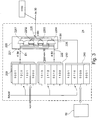
- FIG. 3 shows a block diagram of an exemplary embodiment with a master 3.
- the master 3 is connected to the higher-level fieldbus 9.
- the master 3 has a circuit 60 which can be referred to as a fieldbus interface circuit 60 or also as a processing unit or fieldbus core (FBC). If the processor 50 of the master 2 takes over the process control, the FBC 60 can remain unused or the FBC 60 and the PLC 10 can be dispensed with.
- FBC fieldbus core
- the FBC 60 and the processor 50 are via a parallel bus 55 with a Data management unit 70 and a channel 21 connected.
- the parallel bus 55 is, for example, a 32-bit wide parallel bus.
- the connection 55 can alternatively also be any other connection that allows data transfer between the units.
- the processor 50 is set up to configure the FBC 60, the data management unit 70 and the channel 21.
- the data management unit 70 is set up to transfer data into the channel 21 in order to send the data onto the ring bus 3 in at least one data packet.
- the data can be process data that were received from the FBC 60 via the fieldbus 9 in fieldbus telegrams. Alternatively, the data could also be process data that were generated by processor 50.
- the master 2 has a transceiver circuit 30 which is set up to generate bus-compliant data packets for data transmission on the bus 3 and to insert the data received from channel 21 into the corresponding data packet. Furthermore, the transceiver circuit 30 is set up to receive data packets sent back via the bus 3. Data contained in the received data packets are written into the channel 21 by the transceiver circuit 30. These data can be input from channel 21 via parallel bus 55 by means of data management unit 70 to FBC 60 and / or processor 50 for further processing.
- the master 2 also has a control circuit 40 for controlling the transceiver circuit 30.
- the control takes place in parallel to a program run in the processor 50 and is largely independent of the processor 50.
- the control circuit 40 can also be referred to as a cycle frame generator, the control circuit 40 controlling the transceiver circuit 30 to generate a cycle frame.
- the control circuit 40 is set up to control the transceiver circuit 30 in order to generate a data packet.
- the transceiver circuit 30 starts sending a data packet when the control circuit 40 applies the control signal St to the transceiver circuit 30 via the connection 41. For example, a start pulse, an identifier ILI and the length of the data packet are transmitted to the transceiver circuit 30 by means of the control signal ST.
- the identifier ILI can also be called an index.
- the transceiver circuit 30 informs the control circuit 40 of the end by means of a confirmation signal DN via the connection 42.
- Circuits 21, 30, 40, 60, 70 of the master 2 are preferably implemented on a semiconductor chip 75.
- the semiconductor chip can be designed as an ASIC or FPGA, for example.
- the circuits 21, 30, 40, 60, 70 are preferably separate from the processor 50, so that at least the transceiver circuit 30 and the channel 21 can be operated on the processor 50 independently of a program sequence.
- FIG. 2 an embodiment of a master 2 is shown schematically as a block diagram. It shows a master 2 of a bus system 1 for process control.
- the bus system 1 also has a bus 3 and a first slave 81 and a second slave 82.
- a person skilled in the art is aware that, depending on the scope of the process control, a different number of slaves may be required.
- a data packet P that is generated and sent by a transceiver circuit 30 of the master 2 is also shown schematically.
- the transceiver circuit is set up to send transmit data TD and receive receive data RD for process control by means of data packets P, P '.
- the transceiver circuit 30 is set up to generate the data packet P to be transmitted with a header and a data area.
- the transmitted data packet P is transmitted via the bus 3 to the slaves 81, 82 and sent back to the transceiver circuit 30 of the master 2.
- the data packet P ′ received by the transceiver circuit 30 was originally also generated by the transceiver circuit 30.
- the slaves 81, 82 do not generate any data packets.
- the data packet P transmitted by the transceiver circuit 30 contains transmission data TD.
- the data packet P ′ received by the transceiver circuit 30 contains received data RD.
- Data in the data packet P can be changed by the slaves 81, 82. Accordingly, the transmission data TD and the reception data RD are the same or different. Both send data TD and receive data RD can be required for process control.
- the transceiver circuit 30 is set up, the data packet P 'with a header and to receive a data area via the bus 3 and to read the received data RD from the data area PL of the received data packet P '.
- the master 2 has a channel 21 which is connected to the transceiver circuit 30. In the embodiment of Figure 2 it is shown that the master 2 can also have further channels 22, 23. Of the. Master 2 is set up to select the transmission data TD from one of the channels 21, 22, 23 and to write the transmission data TD from the selected channel 21, 22, 23 into a user data area of the data packet P. Each channel 21, 22, 23 has an associated memory area 210, 230 for its transmission data TD. Transmission data TD from different channels can thus be stored in parallel in the master 2 at the same time. As a result, the bus system 1 can be used in a particularly flexible manner. For example, a reconfiguration during operation is possible.
- each channel 21, 22, 23 has a receive memory area 210, wherein in the Figure 2 only the reception memory area 210 of the channel 21 is shown schematically.
- the receive memory area 210 has at least a corresponding size in order to store all of the received data RD of the received data packet P 'at the same time. This has the advantage that the received data RD are available for one or more data packets to be sent later.
- the received data RD of a data packet are retained in full at least until a subsequent data packet is received.
- the transceiver circuit 30 is set up to write the received data RD of the data packet P ′ received via the bus 3 into the receive memory area 210 of the associated channel 21, 22, 23.
- a different data packet P can be sent with each channel 21, 22, 23.
- the transceiver circuit 30 is set up to generate different data packets P to be transmitted, each with a header and a data area.
- the slaves 81, 82 are set up to distinguish the different data packets.
- the master 2 set up, to write an identifier belonging to the selected channel 21, 22, 23 into the data packet P and to send the data packet P containing the identifier and the transmission data TD to the slaves 81, 82.
- the slaves 81, 82 are set up to receive the data packet P.
- Each slave 81, 82 reads part of the transmission data TD of the master 2 or reads no transmission data TD if, for example, the transmission data TD are not provided for the slave 81.
- Each slave 81, 82 writes part of the received data RD to the master 2 or does not write any received data RD if, for example, no data are to be sent to the master 2.
- the data packet P ′ is sent back in the sequence from the last slave 82 to the master 2 and received by the master 2.
- the master 2 is set up to reassign the received data packet P 'to the selected channel 21, 22, 23 based on the identifier and to store the received data RD of the received data packet P' in the selected channel 21, 22, 23.
- a channel 21, 22, 23 in the sense of the exemplary embodiment of Figure 2 is a hardware circuit that is associated with a specific logical channel of the transmission via bus 3. Correspondingly, channel 21, 22, 23 does not mean the physical transmission channel.
- the channel 21 of the master 2 in the embodiment of Figure 2 has at least one receive memory area 210.
- the transceiver circuit 30 is set up to write the received data RD of the data packet P ′ received via the bus 3 into the receive memory area 210.
- the transceiver circuit 30 continuously checks the signal stream that is sent by the first slave 81. The content of the data field with the received data RD is written from the data packet P 'into the first channel 21 if the data packet P' is logically assigned to the first channel 21.
- the channel 21 of the master 2 has in the exemplary embodiment Figure 2 at least one selection circuit 220.
- the selection circuit 220 has the function of selecting between different inputs 221, 222 pending data and of outputting the selected data at an output 225.
- An output 225 of the selection circuit 220 is in the exemplary embodiment Figure 2 connected to the transceiver circuit 30.
- the inputs 221, 222 and the output 225 can for example be formed by hardware, for example by inputs 221, 222 the output 225 of a multiplexer. Alternatively, the inputs 221, 222 and the output 225 can be formed by addressing.
- selected data can be output to the transceiver circuit 30 by the selection circuit 220.
- the selection circuit 220 has a first input 221 for selecting first data D1.
- the first data D1 can have a different origin, depending on the exemplary embodiment. However, the first data D1 are not obtained from the received data RD. For example, the first data D1 are generated by the processor 50, a microcontroller of the master 2. Other origins of the first data D1 are in the other exemplary embodiments in FIGS Figures 3 and 4th shown.
- the selection circuit 220 has a second input 222.
- the second input 222 of the selection circuit 220 is connected to the receive memory area 210.
- the connection between the receive memory area 210 and the second input 222 is advantageously designed for direct transmission of the received data RD.
- the direct connection is implemented, for example, by means of direct connection lines in an FPGA.
- the direct connection for the direct transfer can be made by a copy machine, for example a DMA controller, for example controlled by a state machine.
- a processor such as a CPU, is not required for the transfer, so that a program in a processor is not interrupted by the transfer and does not require processor resources.
- the reception data RD can be selected in the reception memory area 210 by the selection circuit 220.
- the selection circuit 220 is set up to select the transmission data TD from the first data D1 and the reception data RD written in the reception memory area 210.
- the selection circuit 220 is set up to output the transmission data TD into the transceiver circuit 30 for a data packet P to be transmitted.
- the transceiver circuit 30 generates the data packet P and is set up to write the send data TD into the data area of the data packet P to be sent when the data packet P to be sent is generated.
- Each transmitted data packet P arrives via the bus 3 to the slaves 81, 82 and back to the master 2 and is now received there as the data packet P 'with the received data RD.
- the selection circuit 220 is shown schematically by means of the symbol of a multiplexer. It is clear to the person skilled in the art that the function of the selection circuit 220 can be implemented not only by a multiplexer, but also by an identically acting gate logic or by an identically acting memory addressing.
- the slaves 81, 82 in the embodiment of Figure 2 are set up for a change, that is to say a removal or addition during operation of the bus system 1. If a slave 81 takes part in the communication on the bus 3, it will change the data assigned to it in the send data TD of the data packet P so that the data packet P 'received by the master 2 contains the data changed by the slave 81 in the receive data RD . If, on the other hand, the slave 81 does not take part in the communication on the bus 3 because, for example, the slave fails or is pulled from the bus 3, it can no longer change the data in the data packet P. Accordingly, the slave 81 would not process the data packet P, that is to say it would not overwrite the data assigned to it.
- Figure 3 shows an exemplary embodiment on this subject.
- a channel 21 of a master 2 is shown schematically.
- the channel 21 in Figure 3 has a reception memory area 210 and a selection circuit 220.
- the reception memory area 210 and the selection circuit 220 are connected to a transceiver 30 (not shown).
- the channel 21 has a transmit memory area 230 for storing the first data D1.
- the channel 21 has a control memory area 240.
- the receive memory area 210 and / or the transmit memory area 230 are formed, for example, as part of an overall memory of a semiconductor chip.
- the receive memory area 210 and / or the send memory area 230 has a FIFO functionality.
- the receive memory area 210 and / or the transmit memory area 230 are designed as a buffer, for example.
- the first data D1 in the transmit memory area 230 are, for example, process data that originate from a fieldbus. Accordingly, in the exemplary embodiment Figure 3 the transmit memory area 230 is optionally connected to a fieldbus interface circuit 60 via further circuits and connections of the master 2.
- the fieldbus interface circuit 60 is shown, for example, in FIG Figure 1 shown schematically.
- the fieldbus interface circuit 60 is in the exemplary embodiment from FIG Figure 3 connected to the transmit memory area 230 of the channel 21 for inputting process data received via a fieldbus 9 as the first data D1 into the transmit memory area 230.
- the first data D1 can also originate from the processor 50 of the master 2.
- the selection circuit 220 is set up for bit-granular selection. So that a bit-granular selection can take place, by means of the selection circuit 220, send bits of the send data TD are composed bit by bit from bits of the first data D1 and bits of the received data RD. In the embodiment of Figure 3 a bit width of 4 bits is shown. The person skilled in the art is aware, however, that bit widths of, for example, 8, 16 or 32 bits can be provided in order to select a corresponding number of bits in parallel.
- the first input 221 of the selection circuit 220 for the first data D1 has a bit width of several bits - in this case 4 bits.
- the second input 222 of the selection circuit 220 also has an identical bit width.
- the selection circuit 220 has a switching element 2201, 2202, 2203, 2204 for each of the plurality of bits.
- the switching element 2201, 2202, 2203, 2204 for each bit is a changeover switch in the simplest case.
- the selection circuit 220 is set up in such a way that the switching elements 2201, 2202, 2203, 2204 can be activated independently of one another.
- the selection circuit 220 has a 4-bit wide control input 226.
- the channel 21 advantageously has a control memory area 240 with control values for controlling the selection circuit 220. The control values are applied to the control input 226 of the selection circuit 220.
- FIG Figure 3 In order to synchronize the output of the first data D1 from the transmit memory area 230 and the received data RD and the control values from the control memory area 240, FIG Figure 3 an addressing is provided.
- the memory cells belonging to one another are read out simultaneously using the address RAdd.
- data and control values are associated with one another in all second lines. This is shown schematically by the pointer to the address RAdd .
- the middle bits 0 and 1 of the first data D1 and the outer two bits 1 and 0 of the received data RD are selected by the two ones 1 1 of the control values.
- the selection result is shown schematically in accordance with 1 0 1 0 and at the output 225 of the selection circuit 220.
- the processor 50 of the master 2 is advantageously connected to the control memory area 240, the processor 50 being set up to program the control values in the control memory area 240.
- the transceiver circuit 30 of the master 2 generates a data packet P with transmission data TD for the process control.
- the master 2 writes the transmit data TD from a selected channel 21 into a useful data area of the data packet P.
- the master 2 since further channels 22, 23 can also be provided, in a subsequent step the master 2 generates an identifier ILI (cf. Figure 5 ) written into the data packet P.
- the ILI identifier can also be referred to as an index. The identifier enables both the master 2 and the slaves 81, 82 a simple assignment.
- the transceiver circuit 30 of the master 2 the data packet P containing the identifier ILI and the transmission data TD are sent to the slave 81, 82. If the data packet P has passed all slaves 81, 82, the data packet P sent to the slave 81, 82 is transmitted back to the master 2 and the data packet P 'is received by the transceiver circuit 30.
- the transceiver circuit 30 of the master 2 assigns the receiving data packet P ′ to the selected channel 21 based on the identifier ILI. In this case, the received data RD of the receiving data packet P ′ are stored in the selected channel 21 by the transceiver circuit 30.
- the master 2 is advantageously set up to determine whether a slave, for example 81, does not participate in a bus communication on the bus 3. For example, the number of slaves counted does not match an expected number of slaves. In this way, the master 2 determines in a particularly simple manner that a slave 81 does not participate in the bus communication on the bus 3. This evaluation can be carried out by the processor 50, for example. By querying the bus 3 it can be found out that precisely the slave 81 is no longer participating in the bus communication. In a subsequent step, a part of the received data RD belonging to the determined slave 81 is written by the master 2 into the transmit data TD of the channel 21. For this purpose, the processor 50 writes the corresponding control values in the control memory area 240.
- the last valid data received from the slave 81 which is no longer participating in the communication, is transferred from the received data RD into the transmitted data TD. This has the effect that the last valid data values received by slave 81 are frozen. This is also referred to as the "hold last value" function.
- the advantage of this is that only valid values are used that are out of date but cannot cause process instability.
- standard default values can differ significantly from the last valid value, which can result in significant discontinuities in the system.
- the solution according to the embodiment of FIG Figure 3 the advantage that when communication is resumed by, for example, previously withdrawn and now reinserted slave 81, current values are seamlessly transmitted again, so that the process can be continued uninterrupted.
- FIG 4 an embodiment of a master 2 is shown schematically as a block diagram.
- a bus 3 and a first slave 81 and a second slave 82 are also shown.
- the master 2 has a transceiver circuit 30 and a channel 22.
- the channel 22 has a selection circuit 220 and a reception memory area 210.
- the first data D1 of the channel 22 are present as fixed data at the first input 221 of the selection circuit 220.
- the first data D1 are in the exemplary embodiment Figure 4 formed by connections to high potential and / or low potential. As an example, in Figure 4 shown that the first data D1 are zero values.
- the first data D1 are defined by programming, in particular a non-volatile memory area.
- the reception memory area 210 has a control output 219 for outputting a control signal NE for controlling the selection circuit 220.
- the control output 219 of the receive memory area 210 is connected to a control input 226 of the selection circuit 220.
- the reception memory area 210 is set up to apply a value of the control signal NE based on the reception of the reception data RD to the control input 226 of the selection circuit 220. If, for example, the receive memory area 210 is empty because no valid data packet P 'has yet been received, the value of the control signal NE corresponds to a selection exclusively of the fixed first data D1 by the selection circuit 220 the value of the control signal NE corresponds to a selection exclusively of the received data RD by the selection circuit 220.
- the fixed first data D1 can achieve a defined initial state, and undefined communication is avoided.
- slave-to-slave communication can be achieved.
- channel 22 is set up for slave-to-slave communication.
- the method steps explained below are advantageously carried out.
- the transceiver circuit 30 is activated by the control circuit 40 in order to generate a data packet P associated with the channel 22. Since the receive memory area 210 is still empty, the fixed first data D1 - e.g. exclusively zeros - are written into the user data area of the data packet P by the selection circuit 220. This first data packet P is sent to the slaves 81, 82 via the bus 3.
- the second slave 82 will write this data to be transmitted into the data packet P.
- the data packet P ′ is then received by the transceiver circuit and the received data RD are written into the receive memory area 210 by the transceiver circuit 30.
- the receive data RD stored in the receive memory area 210 of the selected channel 22 are completely written into the transmit data TD.
- the control signal NE has a value that is associated with a non-empty receive memory area 210.
- the transceiver circuit 30 generates a new data packet P with a useful data area in each cycle, but the received data RD are adopted unchanged in the transmit data, so that the useful data area practically circulates in the bus system via the bus 3.
- the transmission is preferably carried out cyclically.
- the transmission of data packets P, P 'between transceiver circuit 30 and slaves 81, 82 is shown schematically.
- the transceiver circuit 30 is set up, to generate the data packet P for the transmitted data TD and, accordingly, also the original data packet of the received data RD.
- the transmitted data TD and the received data RD are used for process control.
- the transceiver circuit 30 has a first finite state machine 310 (German - finite automaton) which is set up to generate the data packet P.
- the first finite state machine 310 is set up to generate the data packet P with a header H and a data area PL for the transmission data TD.
- the data packet can have a trailer T.
- the trailer contains a count value CNT and a check value CRC (Cyclic Redundancy Check).
- the data area PL (English. Payload) contains the data TD, RD and an identifier ILI.
- the data area PL can also be referred to as a user data area.
- the head H has a packet identifier for the type of the transmitted data packet P and control data CD.
- Each data packet P generated and sent by the transceiver circuit 30 is transmitted back to the input 34 of the transceiver circuit 30 via the output 33 and the bus 3 by the slaves 81, 82.
- the received data packet is in Figure 5 designated as P ', since the transmitted transmission data TD in the data area PL can be changed by the slaves 81, 82 and received data RD are received by the transceiver circuit 30 as a result of the change.
- the structure of the sent data packet P and the received data packet P ' is unchanged.
- the length of the data packet P sent and the data packet P 'received is also the same.
- the transceiver circuit 30 has a control input 31. With the control input 31, for example, a control circuit 40, as in FIG Figure 1 or a processor connected.
- the transceiver circuit 30 is set up to generate the data packet P based on a control signal ST at the control input 31.
- a confirmation signal DN can be output at the signal output 32.
- the transceiver circuit 30 is connected to one or more channels 21, 22, 23 via the inputs / outputs 38, 39.
- the transceiver circuit 30 receives a start pulse, an identifier ILI and the length of the data packet P to be sent via the input 31.
- the transceiver circuit is set up to select the channel 21, 22, 23 based on the identifier ILI.
- the transceiver circuit 30 can assign the identifier ILI and the channel 21, 22, 23 with transmit data TD to one another.
- a table LUT (Look Up Table) is provided as the assignment unit 330, into which the identifier ILI is entered on the input side and which addresses the corresponding channel 21, 22, 23 on the output side.
- the table LUT can - as in Figure 5 - be formed in the transceiver circuit 30, or the table LUT is formed outside the transceiver circuit 30 and can be accessed by the transceiver circuit 30.
- another assignment unit 330 can also be provided, for example by means of addressing or the like.
- the first finite state machine 310 of the transceiver circuit 30 is set up, the data packet P for process control with the transmission data. TD and the identifier ILI.
- the transceiver circuit 30 has a second finite state machine 320 and is set up to transfer the received data RD of the received data packet P 'based on the identifier ILI contained in the received data packet P' and the assignment to the channel 21, 22, 23 in the receiving Memory area 210 of the channel 21, 22, 23 associated with the ILI identifier.
- the LUT Look Up Table
- the data bus subscribers 81, 82 are set up to evaluate the data TD, RD in the data packet P by means of instruction lists and the identifier ILI.
- the identifier ILI can also be referred to as an index or an instruction list index.
- the identifier ILI precedes the process data TD, RD in the data packet P, for example. If the first slave 81 recognizes the identifier ILI, for example at the position of the ILI within the data packet P, the first slave stores the data TD in a receive register 810. If the second slave 82 recognizes the identifier ILI, For example, at the position of the ILI within the data packet P, the second slave stores the data TD in its receive register 820.
- the data TD are, for example, copied when they are stored and are then still contained in the user data area PL of the data packet P. Accordingly, the slaves 81, 82 can also write data to the data packet P by changing the data TD already present in the data packet P to later receive data RD.
- the slave 81 has an analog input (not shown), digital input data of a digitized analog signal being written into the useful data area PL of the data packet P. This changes the data packet P and now contains the data of the digitized analog signal as received data RD for the master 2.
- the local bus interface of the master is divided into two parts 33, 34.
- data TD are sent to the local bus 3 via the connection 33 in the downward direction.
- the master 2 writes the transmission data TD from a selected channel 21, 22, 23 into a useful data area PL of the data packet P.
- an identifier ILI belonging to the selected channel 21, 22, 23 is written into the data packet P by the master 2.
- the master 2 sends the data packet P containing the identifier ILI and the transmission data TD to the slave 81, 82. Then the master 2 receives data RD of the data packet P 'via the connection 34 in the upward direction from the local bus 3.
- the data packet P sent to the slave 81, 82 is transmitted back to the master 2.
- the master 2 assigns the receiving data packet P 'based on the identifier ILI to the selected channel 21, 22, 23 and the received data RD of the receiving data packet P' is stored in the selected channel 21, 22, 23.
- the validity of the received data RD is determined, for example, on the basis of the CRC or a valid bit.
- a cycle frame can be defined, for example, as a recurring (cyclical), preferably equidistant, time interval in which data can be transmitted on the ring bus 3.
- the cycle frame has, for example, at least one start identifier and a time range for the transmission of data.
- start identifiers of successive cycle frames are advantageously at an equidistant time interval from one another.
- the mentioned time range is provided for the transmission of the data TD, RD, which can be transmitted within the cycle frame in the form of data packets P, P '.
- the start identifier and the data packets P, P ' are transmitted via the ring bus 3 and pass through all the data bus users, the master 2 and the slaves 81, 82.
- the cycle frame is advantageously initiated by the master 2 in the ring bus 3.
- the start identifier can be transmitted separately, that is to say as an independent symbol, or is advantageously contained in a start data packet.
- Idle data are advantageously inserted in a cycle frame, in particular adjacent to at least one data packet P, P '.
- the transmission of the data packets P, P 'and / or the idle data advantageously brings about an uninterrupted signal on the ring bus 3.
- the signal enables the slaves 81, 82 to synchronize with it in terms of time.
- Each data packet P, P ' is sent from the master 2 in the downward direction to the first slave 81 of the ring bus 3. This receives a first part of the data packet P via its interface.
- the slave 81 then processes the part and then forwards the part to the next slave 82 via its interface, preferably at the same time the first slave 81 receives a second part of the data packet P etc.
- FIG. 6 a block diagram of a master 2 of a further embodiment of the invention is shown schematically.
- That Bus system in Figure 6 also shows two slaves 81, 82 and a local bus 3.
- the master 2 has a transceiver circuit 30 for sending transmission data and receiving reception data via the local bus 3, for example by means of data packets.
- a reception memory area 210 is provided which can be used jointly by both channels 22, 23.
- both channels 22 and 23 have the receive memory area 210.
- the receive memory area 210 has a first buffer 211 and a second buffer 212.
- the buffers 211, 212 are characterized by different address spaces in the. Receive memory area 210 is formed.
- the address A is used for the Figure 6 to write, for example, 32-bit wide memory cells by data blocks D32 by means of a write pointer wp (English - write pointer) or to read them out by means of a read pointer rpf, rpl (English - read pointer).
- the transceiver circuit 30 is set up to write the received data of a data packet received via the local bus 3 into the second buffer 212 by means of the write pointer wp.
- the write pointer wp is controlled by a control circuit 245.
- the write pointer wp controlled by the control circuit 245 points to an address A of the second buffer 212 if previous received data of a previously received data packet is stored as valid received data in the first buffer 211.
- a determination circuit 340 of the transceiver 30 determines whether the received data or the received data packet is valid.
- the transceiver circuit 30 is set up to check the received data of the received data packet and to write the received data into the receive memory area 210.
- Writing the Received data can take place independently of the validity of the received data, with the validity of the received data being stored in the respective buffer 211, 212, for example by means of a flag. If the data stored in the buffer 211, 212 are invalid, they can be overwritten with the following data. Alternatively, it is possible to write the received data to a buffer 211, 212 of the receive memory area 210 only if the test result is positive and to discard it if it is invalid.
- the validity can be transmitted as validity value V from the determination circuit 310 of the transceiver circuit 30 to the control circuit 245 of the selection circuit 220.
- the determination of the validity value V may, for example, using a test value CRC32 (eng -. C yclic R edundancy C tail) or by a transmitted valid bits B.
- the validity bit B is shown, which can be transmitted in higher protocol layers and is used, for example, to ensure that one of the slaves 81, 82 uses the transmitted validity bit B to indicate to the master 2 that the received data sent by slave 81, 82 is invalid due to a slave's own error diagnosis, for example.
- the two possibilities described above are shown schematically with both values V, B. The determination of the validity is not limited to these two examples, so other types of validity can also be used.
- the transceiver circuit 30 is set up to write the received data of a data packet received via the local bus 3 into the first buffer 211 using the write pointer wp if previous received data of a previously received data packet is stored as valid received data in the second buffer 212. This ensures that at least the last valid received data is always in one of the two buffers 211, 212 of the receive memory area 210 and can be used.
- the control circuit 245 is also part of a selection circuit 220 which enables the data D32 stored in the memory area 210 to be selected via at least one read pointer rpl.
- the selection circuit 220 is part of at least one channel 22. In one embodiment of FIG Figure 6 is an output of the selection circuit 220 with the transceiver circuit 30 tied together.
- the selection circuit 220 has, through the read pointer, a first input 221 for selecting first data.
- the first data i.e. the default values
- the data packet reaches the transceiver circuit 30 of the master 2 via the slaves 81, 82, which can change the data in the data packet. If the master 2 receives data in the data packet, these are defined as receive data.
- the transceiver circuit 30 is set up to receive the data packet with a header and a data area via the bus 3 and to read the received data from the data area of the received data packet.
- the transceiver circuit 30 writes the received data into the second buffer 212, since the first buffer 211 contains valid data and the default values after the initialization.
- the selection circuit 220 has a second input in the form of the read pointer rpl, which enables a connection between the receive memory area 210 and the transceiver circuit 30.
- this is shown schematically in that the read pointer rpl is shown in dashed lines for another address A.
- the selection circuit 220 is set up to select the transmission data from the first data and the reception data written in the second buffer 212 of the reception memory area 210 and to output the transmission data to the transceiver circuit 30 for a new data packet to be transmitted.
- the transceiver circuit 30 is set up to send the new data packet to be sent with a header and a data area produce. If - as explained above - valid data is present in the second buffer 212 of the receive memory area 210, the control circuit 245 controls the read pointer rpl accordingly and the data D32 from the lowest address nA2 to the highest address hA2 of the second buffer 212 is transferred to the transceiver 30 copied.
- the connection between the receive memory area 210 and the input of the selection circuit 220 is designed for direct transmission of the received data from the second buffer 212.
- the selection circuit 220 does not need an external processor for this, but can control the direct transmission autonomously, for example by means of a copying process.
- the received data from the second buffer 212 are in the exemplary embodiment of Figure 6 entered unchanged as transmission data in the transceiver circuit 30.
- the transceiver circuit 30 is set up to write this transmission data into the data area of the new data packet to be transmitted when the new data packet to be transmitted is generated.
- the new data packet is in turn transmitted back to the transceiver circuit 30 of the master 2 by the slaves 81, 82.
- the transceiver circuit 30 again checks the validity of the received data in this new data packet.
- the receive data are written into the first buffer 211 of the receive memory area 210, since the valid receive data of the previous data packet was written in the second buffer 212 and is still present. If the new received data of the new data packet in the first buffer is also valid, the determination circuit 340 of the transceiver circuit 30 sends a validity bit B to the control circuit 245 of the selection circuit 220.
- the selection circuit 220 is set up to select the transmission data from the reception memory area 210, the reception data from that from the first buffer 211 or second buffer 212 that originate from the data packet last received and having valid reception data.
- the latest valid received data are now in the first buffer 211. Accordingly, the received data from the first buffer would be copied or shifted as send data into the transceiver circuit for a data packet to be generated subsequently. Accepted the received data in the first buffer 211 would be newer, but invalid, so the valid received data of the last data packet would be selected again with valid received data from the second buffer 212.
- the master 2 also has an interface circuit 60 to a higher-level bus 9 embodied, for example, as a field bus. Furthermore, the selection circuit 220 of the master 2 has a second read pointer rpf, which enables valid received data to be read out from the first buffer 211 or the second buffer 212. The received data of the last data packet with valid received data is transferred (for example copied) into the interface circuit 60 by means of the second read pointer rpf and transmitted via the field bus 9.
- a special channel 23 is assigned in the master 2 for transmission via the fieldbus 9. The channel 23 accordingly has the interface circuit 60 as its own hardware for the function of this channel 23.
Landscapes
- Engineering & Computer Science (AREA)
- Computer Networks & Wireless Communication (AREA)
- Signal Processing (AREA)
- Computer Security & Cryptography (AREA)
- Multimedia (AREA)
- Small-Scale Networks (AREA)
Claims (26)
- Maître (2) d'un système de bus (1) destiné à la commande de processus comportant un esclave (81, 82) et un bus (3), comprenant- un circuit émetteur-récepteur (30) destiné à envoyer des données d'émission (TD) et à recevoir des données de réception (RD) pour la commande de processus au moyen de paquets de données (P, P'),- un canal (21, 22, 23) qui présente une zone de mémoire de réception (210),- le circuit émetteur-récepteur (30) étant aménagé pour écrire dans la zone de mémoire de réception (210) les données de réception (RD) d'un paquet de données reçu (P') sur le bus (3),- le canal (21, 22, 23) présentant au moins un circuit de sélection (220), une sortie (225) du circuit de sélection (220) étant reliée au circuit émetteur-récepteur (30),- le circuit de sélection (220) présentant une première entrée (221) pour sélectionner des premières données (D1),- le circuit de sélection (220) présentant une deuxième entrée (222), la deuxième entrée (222) étant reliée à la zone de mémoire de réception (210), et- le circuit de sélection (220) étant aménagé pour sélectionner les données d'émission (TD) parmi les données de réception (RD) écrites dans la zone de mémoire de réception (210) et pour sortir les données d'émission (TD) dans le circuit émetteur-récepteur (30) pour un paquet de données (P) à envoyer sur le bus (3).
- Maître (2) selon la revendication 1,- le circuit émetteur-récepteur (30) étant aménagé pour générer les paquets de données (P, P') pour les données d'émission (TD) et les données de réception (RD), en particulier avec un en-tête (H) et une zone de données (PL) pour les données d'émission (TD) ou les données de réception (RD).
- Maître (2) selon l'une quelconque des revendications précédentes,- le circuit émetteur-récepteur (30) étant aménagé pour recevoir un paquet de données (P') comportant un en-tête (H) et une zone de données (PL) sur le bus (3), et pour lire les données de réception (RD) à partir de la zone de données (PL) du paquet de données reçu (P').
- Maître (2) selon l'une quelconque des revendications précédentes,- le circuit émetteur-récepteur (30) étant aménagé pour générer un paquet de données (P) à envoyer comportant un en-tête (H) et une zone de données (PL).
- Maître (2) selon l'une quelconque des revendications précédentes,- la liaison entre la zone de mémoire de réception (210) et la deuxième entrée (222) étant réalisée pour la transmission directe des données de réception (RD).
- Maître (2) selon l'une quelconque des revendications précédentes,- le circuit émetteur-récepteur (30) étant aménagé pour écrire les données d'émission (TD) dans la zone de données (PL) du paquet de données (P) à envoyer tout en générant le paquet de données (P) à envoyer.
- Maître (2) selon l'une quelconque des revendications précédentes,- le circuit émetteur-récepteur (30) étant aménagé pour vérifier les données de réception (RD) du paquet de données reçu (P').
- Maître (2) selon l'une quelconque des revendications précédentes,- la zone de mémoire de réception (210) ayant au moins une taille permettant de stocker en même temps toutes les données de réception (RD) du paquet de données reçu (P').
- Maître (2) selon l'une quelconque des revendications précédentes,- la zone de mémoire de réception (210) présentant une première mémoire tampon (211) et une deuxième mémoire tampon (212),- le circuit émetteur-récepteur (30) étant aménagé pouro écrire les données de réception (RD) dans la deuxième mémoire tampon (212) si des données de réception (RD) précédentes d'un paquet de données reçu précédemment sont stockées dans la première mémoire tampon (211) comme des données de réception (RD) valables, ouo écrire les données de réception (RD) dans la première mémoire tampon (211) si des données de réception (RD) précédentes d'un paquet de données reçu précédemment sont stockées dans la deuxième mémoire tampon (212) comme des données de réception (RD) valables.
- Maître (2) selon la revendication 9,- le circuit de sélection (220) pour la sélection des données d'émission (TD) dans la zone de mémoire de réception (210) étant aménagé pour sélectionner les données de réception (RD) dans celle de la première mémoire tampon (211) ou de la deuxième mémoire tampon (212) qui proviennent du paquet de données reçu (P') en dernier et présentant des données de réception (RD) valables.
- Maître (2) selon l'une quelconque des revendications précédentes,- le circuit émetteur-récepteur (30) étant aménagé pour associer le canal (21, 22, 23) aux données d'émission (TD) et/ou aux données de réception (RD) au moyen d'un identifiant (ILI) dans le paquet de données (P, P').
- Maître (2) selon la revendication 11,- le circuit émetteur-récepteur (30) présentant une première machine à états finis (310) et étant aménagé pour générer le paquet de données (P, P') pour la commande de processus avec l'identifiant (ILI) au moyen de la première machine à états finis (310).
- Maître (2) selon l'une des revendications 11 et 12,- le circuit émetteur-récepteur (30) présentant une deuxième machine à états finis (320) et étant aménagé pour écrire dans la zone de mémoire de réception (210) du canal (21, 22, 23) les données de réception (RD) du paquet de données reçu (P') sur la base de l'identifiant (ILI) contenu dans le paquet de données reçu (P') et de l'association au canal (21, 22, 23).
- Maître (2) selon l'une quelconque des revendications précédentes,- le circuit émetteur-récepteur (30) présentant une entrée de commande (31) et étant aménagé pour générer le paquet de données (P) sur la base d'un signal de commande (St) à l'entrée de commande (31).
- Maître (2) selon l'une quelconque des revendications précédentes,- le circuit de sélection (220) étant aménagé pour sélectionner les données d'émission (TD) parmi les premières données (D1) et les données de réception (RD) écrites dans la zone de mémoire de réception (210).
- Maître (2) selon la revendication 15,- le canal (21, 23) présentant une zone de mémoire d'émission (230) pour stocker les premières données (D1).
- Maître (2) selon la revendication 16,- comprenant un circuit d'interface de bus de terrain (60), le circuit d'interface de bus de terrain (60) étant relié à la zone de mémoire d'émission (230) du canal (21, 23) pour entrer des données de processus reçues sur un bus de terrain (9) comme les premières données (D1) dans la zone de mémoire d'émission (230).
- Maître (2) selon l'une quelconque des revendications précédentes,- le circuit de sélection (220) étant aménagé pour la sélection granulaire au niveau du bit dans laquelle le circuit de sélection (220) compose bit par bit des bits d'émission des données d'émission (TD) à partir de bits des premières données (D1) et de bits des données de réception (RD).
- Maître (2) selon l'une quelconque des revendications précédentes,- la première entrée (221) du circuit de sélection (220) présentant pour les premières données (D1) une largeur binaire de plusieurs bits, et- le circuit de sélection (220) présentant un élément de commutation (2201, 2202, 2203, 2204) pour chacun des plusieurs bits,- le circuit de sélection (220) étant aménagé de telle sorte que les éléments de commutation (2201, 2202, 2203, 2204) peuvent être pilotés indépendamment les uns des autres.
- Maître (2) selon l'une quelconque des revendications précédentes,- le canal (21) présentant une zone de mémoire de commande (240) comprenant des valeurs de commande pour commander le circuit de sélection (220).
- Maître (2) selon l'une quelconque des revendications précédentes,- les premières données (D1) du canal (22) étant des données fixes - formées en particulier par des connexions au potentiel haut et/ou au potentiel bas - qui sont appliquées à la première entrée (221) du circuit de sélection (220).
- Maître (2) selon la revendication 21,- la zone de mémoire de réception (210) présentant une sortie de commande (219) pour sortir un signal de commande (NE) pour commander le circuit de sélection (220),- la zone de mémoire de réception (210) étant aménagée pour appliquer une valeur du signal de commande (NE) sur la base de la réception des données de réception (RD) à une entrée (226) du circuit de sélection (220).
- Procédé d'exploitation d'un système de bus (1) destiné à la commande de processus, comportant un maître (2) et un esclave (81, 82),- le maître (2) générant un paquet de données (P) avec des données d'émission (TD) pour la commande de processus,- le maître (2) écrivant les données d'émission (TD) à partir d'un canal sélectionné (21, 22, 23) dans une zone de données utiles (PL) du paquet de données (P),- le maître (2) écrivant dans le paquet de données (P) un identifiant (ILI) associé au canal sélectionné (21, 22, 23),- le maître (2) envoyant à l'esclave (81, 82) le paquet de données (P) contenant l'identifiant (ILI) et les données d'émission (TD),- le paquet de données (P) envoyé à l'esclave (81, 82) étant retransmis au maître (2) et le paquet de données (P') étant reçu par le maître (2),- le maître (2) associant le paquet de données reçu (P') au canal sélectionné (21, 22, 23) sur la base de l'identifiant (ILI),- les données de réception (RD) du paquet de données reçu (P') étant stockées dans le canal sélectionné (21, 22, 23), et- au moins une partie des données de réception (RD) stockées dans le canal sélectionné (21, 22, 23) étant écrites dans les données d'émission (TD) pour un paquet de données (P) à envoyer par la suite sur le bus (3).
- Procédé selon la revendication 23,- le maître (2) déterminant une non participation d'un esclave (81) à une communication de bus sur le bus (3),- le maître (2) écrivant une partie des données de réception (RD), associée à l'esclave (81) déterminé dans les données d'émission (TD) du canal (21, 22, 23).
- Procédé selon la revendication 23,- dans lequel, les données de réception (RD) stockées dans le canal sélectionné (21, 22, 23) sont écrites entièrement dans les données d'émission (TD) pour un paquet de données (P) à envoyer par la suite.
- Système de bus (1) destiné à la commande de processus, comprenant un maître (2) et un esclave (81, 82),- le maître (2) étant aménagé pour générer un paquet de données (P) avec des données d'émission (TD) pour la commande de processus,- le maître (2) étant aménagé pour écrire les données d'émission (TD) à partir d'un canal sélectionné (21, 22, 23) dans une zone de données utiles (PL) du paquet de données (P),- chaque canal (21, 22, 23) présentant respectivement une zone de mémoire associée (210, 230) pour ses données d'émission (TD),- le maître (2) étant aménagé pour écrire un identifiant (ILI) associé au canal sélectionné (21, 22, 23) dans le paquet de données (P),- le maître (2) étant aménagé pour envoyer à l'esclave (81, 82) le paquet de données (P) contenant l'identifiant (ILI) et les données d'émission (TD),- l'esclave (81, 82) étant aménagé pour recevoir le paquet de données (P), pour lire sur la base de l'identifiant (ILI) au moins une partie des données d'émission (TD), et/ou pour envoyer au moins une partie des données de réception et renvoyer le paquet de données (P') au maître (2),- le maître (2) étant aménagé pour recevoir le paquet de données (P'),- le maître (2) étant aménagé pour associer au canal sélectionné (21, 22, 23) le paquet de données reçu (P') sur la base de l'identifiant (ILI), et- le maître (2) étant aménagé pour stocker les données de réception (RD) du paquet de données reçu (P') dans le canal sélectionné (21, 22, 23), et- le maître (2) étant aménagé pour écrire dans les données d'émission (TD) au moins une partie des données de réception (RD) stockées dans le canal sélectionné (21, 22, 23) pour un paquet de données (P) à envoyer par la suite sur le bus (3).
Applications Claiming Priority (2)
| Application Number | Priority Date | Filing Date | Title |
|---|---|---|---|
| DE102017008186.7A DE102017008186B4 (de) | 2017-08-31 | 2017-08-31 | Master eines Bussystems |
| PCT/IB2018/000810 WO2019043447A1 (fr) | 2017-08-31 | 2018-07-27 | Maître d'un système de bus |
Publications (2)
| Publication Number | Publication Date |
|---|---|
| EP3676995A1 EP3676995A1 (fr) | 2020-07-08 |
| EP3676995B1 true EP3676995B1 (fr) | 2021-10-06 |
Family
ID=63364093
Family Applications (1)
| Application Number | Title | Priority Date | Filing Date |
|---|---|---|---|
| EP18759373.6A Active EP3676995B1 (fr) | 2017-08-31 | 2018-07-27 | Maître d'un système de bus |
Country Status (5)
| Country | Link |
|---|---|
| US (1) | US11296903B2 (fr) |
| EP (1) | EP3676995B1 (fr) |
| CN (1) | CN111052682B (fr) |
| DE (1) | DE102017008186B4 (fr) |
| WO (1) | WO2019043447A1 (fr) |
Families Citing this family (1)
| Publication number | Priority date | Publication date | Assignee | Title |
|---|---|---|---|---|
| DE102021206498A1 (de) * | 2021-06-23 | 2022-12-29 | Siemens Healthcare Gmbh | Datenübertragungseinrichtung, medizinische Bildgebungseinrichtung und Verfahren zur Übertragung von Datenpaketen |
Family Cites Families (24)
| Publication number | Priority date | Publication date | Assignee | Title |
|---|---|---|---|---|
| US4636858A (en) * | 1984-10-30 | 1987-01-13 | The United States Of America As Represented By The Secretary Of The Air Force | Extracting digital data from a bus and multiplexing it with a video signal |
| DE69321426T2 (de) * | 1992-06-05 | 1999-03-04 | Compaq Computer Corp., Houston, Tex. 77070 | Plattenantriebsteuergerät mit Nachschreibcachespeicher |
| JP3904244B2 (ja) * | 1993-09-17 | 2007-04-11 | 株式会社ルネサステクノロジ | シングル・チップ・データ処理装置 |
| US6735683B2 (en) * | 1994-09-14 | 2004-05-11 | Hitachi, Ltd. | Single-chip microcomputer with hierarchical internal bus structure having data and address signal lines coupling CPU with other processing elements |
| CN1067195C (zh) * | 1996-09-12 | 2001-06-13 | 中国科学院空间科学与应用研究中心 | 一种高速多路复接器及其实现方法 |
| JPH10334037A (ja) * | 1997-05-30 | 1998-12-18 | Sanyo Electric Co Ltd | 通信dma装置 |
| EP0901081B1 (fr) * | 1997-07-08 | 2010-04-07 | Texas Instruments Inc. | Processeur numérique de traitement de signal comprenant des appareils périphériques et des interfaces externes |
| US6553432B1 (en) * | 1999-10-26 | 2003-04-22 | Dell Usa, L.P. | Method and system for selecting IDE devices |
| DE10006265B4 (de) | 2000-02-12 | 2006-03-09 | Phoenix Contact Gmbh & Co. Kg | Vorrichtung zum Steuern des Datenaustauschs in einem Kommunikationsteilnehmer |
| US20050198425A1 (en) * | 2004-03-05 | 2005-09-08 | Wang Liang-Yun | Combined optical storage and flash card reader using single ide or sata port and method thereof |
| US7209989B2 (en) * | 2004-09-29 | 2007-04-24 | Intel Corporation | Transfer acknowledgement mechanism for an MSL architecture |
| CN101098211B (zh) * | 2005-06-30 | 2012-01-25 | 株式会社日立制作所 | 发送控制装置、接收控制装置、以及通信系统 |
| US7826411B2 (en) * | 2007-05-10 | 2010-11-02 | Broadcom Corporation | Cooperative transceiving between wireless interface devices of a host device with shared modules |
| US7881746B2 (en) * | 2007-05-10 | 2011-02-01 | Broadcom Corporation | Shared processing between wireless interface devices of a host device |
| DE102008019277B4 (de) * | 2008-04-16 | 2013-07-18 | Phoenix Contact Gmbh & Co. Kg | Datenübertragungsvorrichtung |
| US8230117B2 (en) * | 2009-04-09 | 2012-07-24 | International Business Machines Corporation | Techniques for write-after-write ordering in a coherency managed processor system that employs a command pipeline |
| KR101025674B1 (ko) * | 2010-02-03 | 2011-03-30 | 엘에스산전 주식회사 | 듀얼 포트를 갖는 이더넷 시스템의 스위칭 장치 |
| DE102010020446B4 (de) * | 2010-05-12 | 2012-12-06 | Wago Verwaltungsgesellschaft Mbh | Automatisierungsgerät und Verfahren zur beschleunigten Verarbeitung von selektierten Prozessdaten |
| DE102011007437A1 (de) * | 2010-11-15 | 2012-05-16 | Continental Teves Ag & Co. Ohg | Verfahren und Schaltungsanrodnung zur Datenübertragung zwischen Prozessorbausteinen |
| EP2557464B1 (fr) * | 2011-08-12 | 2015-07-29 | Siemens Aktiengesellschaft | Procédé destiné au fonctionnement d'un système d'automatisation |
| US8880819B2 (en) * | 2011-12-13 | 2014-11-04 | Micron Technology, Inc. | Memory apparatuses, computer systems and methods for ordering memory responses |
| WO2014156282A1 (fr) * | 2013-03-25 | 2014-10-02 | 三菱電機株式会社 | Maître de bus, système de bus et procédé de commande de bus |
| US10838908B2 (en) * | 2018-07-20 | 2020-11-17 | Xilinx, Inc. | Configurable network-on-chip for a programmable device |
| US10750377B1 (en) * | 2019-03-28 | 2020-08-18 | Integrated Device Technology, Inc. | Multi-mode control with fast-access lookup table implementation |
-
2017
- 2017-08-31 DE DE102017008186.7A patent/DE102017008186B4/de active Active
-
2018
- 2018-07-27 CN CN201880055128.4A patent/CN111052682B/zh active Active
- 2018-07-27 EP EP18759373.6A patent/EP3676995B1/fr active Active
- 2018-07-27 WO PCT/IB2018/000810 patent/WO2019043447A1/fr unknown
-
2020
- 2020-02-28 US US16/805,411 patent/US11296903B2/en active Active
Also Published As
| Publication number | Publication date |
|---|---|
| US20200204398A1 (en) | 2020-06-25 |
| DE102017008186B4 (de) | 2022-12-15 |
| US11296903B2 (en) | 2022-04-05 |
| WO2019043447A1 (fr) | 2019-03-07 |
| DE102017008186A1 (de) | 2019-02-28 |
| CN111052682B (zh) | 2022-05-24 |
| CN111052682A (zh) | 2020-04-21 |
| EP3676995A1 (fr) | 2020-07-08 |
Similar Documents
| Publication | Publication Date | Title |
|---|---|---|
| DE3300261C2 (fr) | ||
| DE102007004044B4 (de) | Verfahren und Anlage zur optimierten Übertragung von Daten zwischen einer Steuereinrichtung und mehreren Feldgeräten | |
| EP1787204B1 (fr) | Gestionnaire de messages et procede pour commander l'acces a des donnees d'une memoire de messages d'un module de communication | |
| EP1502400B1 (fr) | Procede et systeme de transmission de donnees par des reseaux de donnees commutables | |
| WO2003054644A2 (fr) | Procede de transmission de donnees, systeme de bus seriel et unite de connexion pour un utilisateur de bus passif | |
| EP3759871B1 (fr) | Système de bus maître-esclave et procédé de fonctionnement d'un système de bus | |
| EP1776807A1 (fr) | Procede et dispositif permettant d'acceder a des donnees d'une memoire de messages d'un module de communication | |
| DE102005048581B4 (de) | Teilnehmerschnittstelle zwischen einem FlexRay-Kommunikationsbaustein und einem FlexRay-Teilnehmer und Verfahren zur Übertragung von Botschaften über eine solche Schnittstelle | |
| WO2006015908A1 (fr) | Procede de mise en memoire de messages dans une memoire de messages et memoire de messages associee | |
| EP3685236A1 (fr) | Circuit pour connecter un bus de terrain et un bus local | |
| EP3676995B1 (fr) | Maître d'un système de bus | |
| EP1133106B1 (fr) | Dispositif de commande d'échange de données dans un terminal de communication | |
| WO2004025493A1 (fr) | Circuit intégré avec commutation par multiplexeurs entre fonctionnement normal et fonctionnement d'essai | |
| EP3072250B1 (fr) | Dispositif de communication, système de communication et procédé de transmission synchronisée de télégrammes | |
| WO2003028320A1 (fr) | Procede pour l'exploitation d'un systeme de communication cyclique isochrone | |
| EP1430654A1 (fr) | Procede pour la generation d'une table d'adresses statique et reseau de donnees | |
| EP1371184B1 (fr) | Circuit de commutation electronique et procede destines a une interface de communication avec memoire tampon intermediaire | |
| DE102017002806B4 (de) | Koppler für ein Automatisierungssystem | |
| DE102018010209A1 (de) | Master-Slave Bussystem und Verfahren zum Betrieb eines Bussystems | |
| DE69315785T2 (de) | Modulare Vorrichtung zum Koppeln und zum Multiplexen von unterschiedlichen Bussen | |
| DE10141187B4 (de) | Elektronischer Schaltkreis und Verfahren für eine Kommunikationsschnittstelle mit Zwischenspeicherung | |
| EP1371193B1 (fr) | Circuit electronique et procede pour interface de communication a memoire tampon pseudo-transit | |
| EP3824393A1 (fr) | Circuit de transmission de données avec mise en mémoire tampon | |
| DE102017216991B4 (de) | Kommunikationsbaustein und Vorrichtung zur Datenübertragung | |
| EP1430657B1 (fr) | Procede pour la creation d'une table d'adresses dynamique pour un noeud de couplage dans un reseau de donnees et procede pour la transmission d'un telegramme de donnees |
Legal Events
| Date | Code | Title | Description |
|---|---|---|---|
| STAA | Information on the status of an ep patent application or granted ep patent |
Free format text: STATUS: UNKNOWN |
|
| STAA | Information on the status of an ep patent application or granted ep patent |
Free format text: STATUS: THE INTERNATIONAL PUBLICATION HAS BEEN MADE |
|
| PUAI | Public reference made under article 153(3) epc to a published international application that has entered the european phase |
Free format text: ORIGINAL CODE: 0009012 |
|
| STAA | Information on the status of an ep patent application or granted ep patent |
Free format text: STATUS: REQUEST FOR EXAMINATION WAS MADE |
|
| 17P | Request for examination filed |
Effective date: 20200213 |
|
| AK | Designated contracting states |
Kind code of ref document: A1 Designated state(s): AL AT BE BG CH CY CZ DE DK EE ES FI FR GB GR HR HU IE IS IT LI LT LU LV MC MK MT NL NO PL PT RO RS SE SI SK SM TR |
|
| AX | Request for extension of the european patent |
Extension state: BA ME |
|
| DAV | Request for validation of the european patent (deleted) | ||
| DAX | Request for extension of the european patent (deleted) | ||
| GRAP | Despatch of communication of intention to grant a patent |
Free format text: ORIGINAL CODE: EPIDOSNIGR1 |
|
| STAA | Information on the status of an ep patent application or granted ep patent |
Free format text: STATUS: GRANT OF PATENT IS INTENDED |
|
| INTG | Intention to grant announced |
Effective date: 20210601 |
|
| GRAS | Grant fee paid |
Free format text: ORIGINAL CODE: EPIDOSNIGR3 |
|
| GRAA | (expected) grant |
Free format text: ORIGINAL CODE: 0009210 |
|
| STAA | Information on the status of an ep patent application or granted ep patent |
Free format text: STATUS: THE PATENT HAS BEEN GRANTED |
|
| AK | Designated contracting states |
Kind code of ref document: B1 Designated state(s): AL AT BE BG CH CY CZ DE DK EE ES FI FR GB GR HR HU IE IS IT LI LT LU LV MC MK MT NL NO PL PT RO RS SE SI SK SM TR |
|
| REG | Reference to a national code |
Ref country code: GB Ref legal event code: FG4D Free format text: NOT ENGLISH |
|
| REG | Reference to a national code |
Ref country code: CH Ref legal event code: EP Ref country code: AT Ref legal event code: REF Ref document number: 1437183 Country of ref document: AT Kind code of ref document: T Effective date: 20211015 |
|
| REG | Reference to a national code |
Ref country code: DE Ref legal event code: R096 Ref document number: 502018007378 Country of ref document: DE |
|
| REG | Reference to a national code |
Ref country code: IE Ref legal event code: FG4D Free format text: LANGUAGE OF EP DOCUMENT: GERMAN |
|
| REG | Reference to a national code |
Ref country code: LT Ref legal event code: MG9D |
|
| REG | Reference to a national code |
Ref country code: NL Ref legal event code: MP Effective date: 20211006 |
|
| PG25 | Lapsed in a contracting state [announced via postgrant information from national office to epo] |
Ref country code: RS Free format text: LAPSE BECAUSE OF FAILURE TO SUBMIT A TRANSLATION OF THE DESCRIPTION OR TO PAY THE FEE WITHIN THE PRESCRIBED TIME-LIMIT Effective date: 20211006 Ref country code: LT Free format text: LAPSE BECAUSE OF FAILURE TO SUBMIT A TRANSLATION OF THE DESCRIPTION OR TO PAY THE FEE WITHIN THE PRESCRIBED TIME-LIMIT Effective date: 20211006 Ref country code: FI Free format text: LAPSE BECAUSE OF FAILURE TO SUBMIT A TRANSLATION OF THE DESCRIPTION OR TO PAY THE FEE WITHIN THE PRESCRIBED TIME-LIMIT Effective date: 20211006 Ref country code: BG Free format text: LAPSE BECAUSE OF FAILURE TO SUBMIT A TRANSLATION OF THE DESCRIPTION OR TO PAY THE FEE WITHIN THE PRESCRIBED TIME-LIMIT Effective date: 20220106 |
|
| PG25 | Lapsed in a contracting state [announced via postgrant information from national office to epo] |
Ref country code: IS Free format text: LAPSE BECAUSE OF FAILURE TO SUBMIT A TRANSLATION OF THE DESCRIPTION OR TO PAY THE FEE WITHIN THE PRESCRIBED TIME-LIMIT Effective date: 20220206 Ref country code: SE Free format text: LAPSE BECAUSE OF FAILURE TO SUBMIT A TRANSLATION OF THE DESCRIPTION OR TO PAY THE FEE WITHIN THE PRESCRIBED TIME-LIMIT Effective date: 20211006 Ref country code: PT Free format text: LAPSE BECAUSE OF FAILURE TO SUBMIT A TRANSLATION OF THE DESCRIPTION OR TO PAY THE FEE WITHIN THE PRESCRIBED TIME-LIMIT Effective date: 20220207 Ref country code: PL Free format text: LAPSE BECAUSE OF FAILURE TO SUBMIT A TRANSLATION OF THE DESCRIPTION OR TO PAY THE FEE WITHIN THE PRESCRIBED TIME-LIMIT Effective date: 20211006 Ref country code: NO Free format text: LAPSE BECAUSE OF FAILURE TO SUBMIT A TRANSLATION OF THE DESCRIPTION OR TO PAY THE FEE WITHIN THE PRESCRIBED TIME-LIMIT Effective date: 20220106 Ref country code: NL Free format text: LAPSE BECAUSE OF FAILURE TO SUBMIT A TRANSLATION OF THE DESCRIPTION OR TO PAY THE FEE WITHIN THE PRESCRIBED TIME-LIMIT Effective date: 20211006 Ref country code: LV Free format text: LAPSE BECAUSE OF FAILURE TO SUBMIT A TRANSLATION OF THE DESCRIPTION OR TO PAY THE FEE WITHIN THE PRESCRIBED TIME-LIMIT Effective date: 20211006 Ref country code: HR Free format text: LAPSE BECAUSE OF FAILURE TO SUBMIT A TRANSLATION OF THE DESCRIPTION OR TO PAY THE FEE WITHIN THE PRESCRIBED TIME-LIMIT Effective date: 20211006 Ref country code: GR Free format text: LAPSE BECAUSE OF FAILURE TO SUBMIT A TRANSLATION OF THE DESCRIPTION OR TO PAY THE FEE WITHIN THE PRESCRIBED TIME-LIMIT Effective date: 20220107 Ref country code: ES Free format text: LAPSE BECAUSE OF FAILURE TO SUBMIT A TRANSLATION OF THE DESCRIPTION OR TO PAY THE FEE WITHIN THE PRESCRIBED TIME-LIMIT Effective date: 20211006 |
|
| REG | Reference to a national code |
Ref country code: DE Ref legal event code: R097 Ref document number: 502018007378 Country of ref document: DE |
|
| PG25 | Lapsed in a contracting state [announced via postgrant information from national office to epo] |
Ref country code: SM Free format text: LAPSE BECAUSE OF FAILURE TO SUBMIT A TRANSLATION OF THE DESCRIPTION OR TO PAY THE FEE WITHIN THE PRESCRIBED TIME-LIMIT Effective date: 20211006 Ref country code: SK Free format text: LAPSE BECAUSE OF FAILURE TO SUBMIT A TRANSLATION OF THE DESCRIPTION OR TO PAY THE FEE WITHIN THE PRESCRIBED TIME-LIMIT Effective date: 20211006 Ref country code: RO Free format text: LAPSE BECAUSE OF FAILURE TO SUBMIT A TRANSLATION OF THE DESCRIPTION OR TO PAY THE FEE WITHIN THE PRESCRIBED TIME-LIMIT Effective date: 20211006 Ref country code: EE Free format text: LAPSE BECAUSE OF FAILURE TO SUBMIT A TRANSLATION OF THE DESCRIPTION OR TO PAY THE FEE WITHIN THE PRESCRIBED TIME-LIMIT Effective date: 20211006 Ref country code: DK Free format text: LAPSE BECAUSE OF FAILURE TO SUBMIT A TRANSLATION OF THE DESCRIPTION OR TO PAY THE FEE WITHIN THE PRESCRIBED TIME-LIMIT Effective date: 20211006 Ref country code: CZ Free format text: LAPSE BECAUSE OF FAILURE TO SUBMIT A TRANSLATION OF THE DESCRIPTION OR TO PAY THE FEE WITHIN THE PRESCRIBED TIME-LIMIT Effective date: 20211006 |
|
| PLBE | No opposition filed within time limit |
Free format text: ORIGINAL CODE: 0009261 |
|
| STAA | Information on the status of an ep patent application or granted ep patent |
Free format text: STATUS: NO OPPOSITION FILED WITHIN TIME LIMIT |
|
| 26N | No opposition filed |
Effective date: 20220707 |
|
| PG25 | Lapsed in a contracting state [announced via postgrant information from national office to epo] |
Ref country code: AL Free format text: LAPSE BECAUSE OF FAILURE TO SUBMIT A TRANSLATION OF THE DESCRIPTION OR TO PAY THE FEE WITHIN THE PRESCRIBED TIME-LIMIT Effective date: 20211006 |
|
| PG25 | Lapsed in a contracting state [announced via postgrant information from national office to epo] |
Ref country code: SI Free format text: LAPSE BECAUSE OF FAILURE TO SUBMIT A TRANSLATION OF THE DESCRIPTION OR TO PAY THE FEE WITHIN THE PRESCRIBED TIME-LIMIT Effective date: 20211006 |
|
| PG25 | Lapsed in a contracting state [announced via postgrant information from national office to epo] |
Ref country code: MC Free format text: LAPSE BECAUSE OF FAILURE TO SUBMIT A TRANSLATION OF THE DESCRIPTION OR TO PAY THE FEE WITHIN THE PRESCRIBED TIME-LIMIT Effective date: 20211006 |
|
| GBPC | Gb: european patent ceased through non-payment of renewal fee |
Effective date: 20220727 |
|
| REG | Reference to a national code |
Ref country code: BE Ref legal event code: MM Effective date: 20220731 |
|
| PG25 | Lapsed in a contracting state [announced via postgrant information from national office to epo] |
Ref country code: LU Free format text: LAPSE BECAUSE OF NON-PAYMENT OF DUE FEES Effective date: 20220727 |
|
| PG25 | Lapsed in a contracting state [announced via postgrant information from national office to epo] |
Ref country code: GB Free format text: LAPSE BECAUSE OF NON-PAYMENT OF DUE FEES Effective date: 20220727 Ref country code: BE Free format text: LAPSE BECAUSE OF NON-PAYMENT OF DUE FEES Effective date: 20220731 |
|
| P01 | Opt-out of the competence of the unified patent court (upc) registered |
Effective date: 20230516 |
|
| PG25 | Lapsed in a contracting state [announced via postgrant information from national office to epo] |
Ref country code: IE Free format text: LAPSE BECAUSE OF NON-PAYMENT OF DUE FEES Effective date: 20220727 |
|
| PGFP | Annual fee paid to national office [announced via postgrant information from national office to epo] |
Ref country code: IT Payment date: 20230721 Year of fee payment: 6 Ref country code: CH Payment date: 20230801 Year of fee payment: 6 Ref country code: AT Payment date: 20230718 Year of fee payment: 6 |
|
| PGFP | Annual fee paid to national office [announced via postgrant information from national office to epo] |
Ref country code: FR Payment date: 20230725 Year of fee payment: 6 Ref country code: DE Payment date: 20230726 Year of fee payment: 6 |
|
| PG25 | Lapsed in a contracting state [announced via postgrant information from national office to epo] |
Ref country code: MK Free format text: LAPSE BECAUSE OF FAILURE TO SUBMIT A TRANSLATION OF THE DESCRIPTION OR TO PAY THE FEE WITHIN THE PRESCRIBED TIME-LIMIT Effective date: 20211006 Ref country code: CY Free format text: LAPSE BECAUSE OF FAILURE TO SUBMIT A TRANSLATION OF THE DESCRIPTION OR TO PAY THE FEE WITHIN THE PRESCRIBED TIME-LIMIT Effective date: 20211006 |
|
| PG25 | Lapsed in a contracting state [announced via postgrant information from national office to epo] |
Ref country code: HU Free format text: LAPSE BECAUSE OF FAILURE TO SUBMIT A TRANSLATION OF THE DESCRIPTION OR TO PAY THE FEE WITHIN THE PRESCRIBED TIME-LIMIT; INVALID AB INITIO Effective date: 20180727 |
|
| PG25 | Lapsed in a contracting state [announced via postgrant information from national office to epo] |
Ref country code: MT Free format text: LAPSE BECAUSE OF FAILURE TO SUBMIT A TRANSLATION OF THE DESCRIPTION OR TO PAY THE FEE WITHIN THE PRESCRIBED TIME-LIMIT Effective date: 20211006 |