EP3675114A1 - Goa circuit - Google Patents
Goa circuit Download PDFInfo
- Publication number
- EP3675114A1 EP3675114A1 EP17922764.0A EP17922764A EP3675114A1 EP 3675114 A1 EP3675114 A1 EP 3675114A1 EP 17922764 A EP17922764 A EP 17922764A EP 3675114 A1 EP3675114 A1 EP 3675114A1
- Authority
- EP
- European Patent Office
- Prior art keywords
- node
- tft
- source
- output end
- signal output
- Prior art date
- Legal status (The legal status is an assumption and is not a legal conclusion. Google has not performed a legal analysis and makes no representation as to the accuracy of the status listed.)
- Withdrawn
Links
Images

Classifications
-
- G—PHYSICS
- G09—EDUCATION; CRYPTOGRAPHY; DISPLAY; ADVERTISING; SEALS
- G09G—ARRANGEMENTS OR CIRCUITS FOR CONTROL OF INDICATING DEVICES USING STATIC MEANS TO PRESENT VARIABLE INFORMATION
- G09G3/00—Control arrangements or circuits, of interest only in connection with visual indicators other than cathode-ray tubes
- G09G3/20—Control arrangements or circuits, of interest only in connection with visual indicators other than cathode-ray tubes for presentation of an assembly of a number of characters, e.g. a page, by composing the assembly by combination of individual elements arranged in a matrix no fixed position being assigned to or needed to be assigned to the individual characters or partial characters
- G09G3/22—Control arrangements or circuits, of interest only in connection with visual indicators other than cathode-ray tubes for presentation of an assembly of a number of characters, e.g. a page, by composing the assembly by combination of individual elements arranged in a matrix no fixed position being assigned to or needed to be assigned to the individual characters or partial characters using controlled light sources
- G09G3/30—Control arrangements or circuits, of interest only in connection with visual indicators other than cathode-ray tubes for presentation of an assembly of a number of characters, e.g. a page, by composing the assembly by combination of individual elements arranged in a matrix no fixed position being assigned to or needed to be assigned to the individual characters or partial characters using controlled light sources using electroluminescent panels
- G09G3/32—Control arrangements or circuits, of interest only in connection with visual indicators other than cathode-ray tubes for presentation of an assembly of a number of characters, e.g. a page, by composing the assembly by combination of individual elements arranged in a matrix no fixed position being assigned to or needed to be assigned to the individual characters or partial characters using controlled light sources using electroluminescent panels semiconductive, e.g. using light-emitting diodes [LED]
- G09G3/3208—Control arrangements or circuits, of interest only in connection with visual indicators other than cathode-ray tubes for presentation of an assembly of a number of characters, e.g. a page, by composing the assembly by combination of individual elements arranged in a matrix no fixed position being assigned to or needed to be assigned to the individual characters or partial characters using controlled light sources using electroluminescent panels semiconductive, e.g. using light-emitting diodes [LED] organic, e.g. using organic light-emitting diodes [OLED]
- G09G3/3225—Control arrangements or circuits, of interest only in connection with visual indicators other than cathode-ray tubes for presentation of an assembly of a number of characters, e.g. a page, by composing the assembly by combination of individual elements arranged in a matrix no fixed position being assigned to or needed to be assigned to the individual characters or partial characters using controlled light sources using electroluminescent panels semiconductive, e.g. using light-emitting diodes [LED] organic, e.g. using organic light-emitting diodes [OLED] using an active matrix
-
- G—PHYSICS
- G09—EDUCATION; CRYPTOGRAPHY; DISPLAY; ADVERTISING; SEALS
- G09G—ARRANGEMENTS OR CIRCUITS FOR CONTROL OF INDICATING DEVICES USING STATIC MEANS TO PRESENT VARIABLE INFORMATION
- G09G3/00—Control arrangements or circuits, of interest only in connection with visual indicators other than cathode-ray tubes
- G09G3/20—Control arrangements or circuits, of interest only in connection with visual indicators other than cathode-ray tubes for presentation of an assembly of a number of characters, e.g. a page, by composing the assembly by combination of individual elements arranged in a matrix no fixed position being assigned to or needed to be assigned to the individual characters or partial characters
- G09G3/22—Control arrangements or circuits, of interest only in connection with visual indicators other than cathode-ray tubes for presentation of an assembly of a number of characters, e.g. a page, by composing the assembly by combination of individual elements arranged in a matrix no fixed position being assigned to or needed to be assigned to the individual characters or partial characters using controlled light sources
- G09G3/30—Control arrangements or circuits, of interest only in connection with visual indicators other than cathode-ray tubes for presentation of an assembly of a number of characters, e.g. a page, by composing the assembly by combination of individual elements arranged in a matrix no fixed position being assigned to or needed to be assigned to the individual characters or partial characters using controlled light sources using electroluminescent panels
- G09G3/32—Control arrangements or circuits, of interest only in connection with visual indicators other than cathode-ray tubes for presentation of an assembly of a number of characters, e.g. a page, by composing the assembly by combination of individual elements arranged in a matrix no fixed position being assigned to or needed to be assigned to the individual characters or partial characters using controlled light sources using electroluminescent panels semiconductive, e.g. using light-emitting diodes [LED]
- G09G3/3208—Control arrangements or circuits, of interest only in connection with visual indicators other than cathode-ray tubes for presentation of an assembly of a number of characters, e.g. a page, by composing the assembly by combination of individual elements arranged in a matrix no fixed position being assigned to or needed to be assigned to the individual characters or partial characters using controlled light sources using electroluminescent panels semiconductive, e.g. using light-emitting diodes [LED] organic, e.g. using organic light-emitting diodes [OLED]
- G09G3/3266—Details of drivers for scan electrodes
-
- G—PHYSICS
- G09—EDUCATION; CRYPTOGRAPHY; DISPLAY; ADVERTISING; SEALS
- G09G—ARRANGEMENTS OR CIRCUITS FOR CONTROL OF INDICATING DEVICES USING STATIC MEANS TO PRESENT VARIABLE INFORMATION
- G09G3/00—Control arrangements or circuits, of interest only in connection with visual indicators other than cathode-ray tubes
- G09G3/20—Control arrangements or circuits, of interest only in connection with visual indicators other than cathode-ray tubes for presentation of an assembly of a number of characters, e.g. a page, by composing the assembly by combination of individual elements arranged in a matrix no fixed position being assigned to or needed to be assigned to the individual characters or partial characters
- G09G3/34—Control arrangements or circuits, of interest only in connection with visual indicators other than cathode-ray tubes for presentation of an assembly of a number of characters, e.g. a page, by composing the assembly by combination of individual elements arranged in a matrix no fixed position being assigned to or needed to be assigned to the individual characters or partial characters by control of light from an independent source
- G09G3/36—Control arrangements or circuits, of interest only in connection with visual indicators other than cathode-ray tubes for presentation of an assembly of a number of characters, e.g. a page, by composing the assembly by combination of individual elements arranged in a matrix no fixed position being assigned to or needed to be assigned to the individual characters or partial characters by control of light from an independent source using liquid crystals
- G09G3/3611—Control of matrices with row and column drivers
- G09G3/3674—Details of drivers for scan electrodes
-
- G—PHYSICS
- G11—INFORMATION STORAGE
- G11C—STATIC STORES
- G11C19/00—Digital stores in which the information is moved stepwise, e.g. shift registers
- G11C19/18—Digital stores in which the information is moved stepwise, e.g. shift registers using capacitors as main elements of the stages
- G11C19/182—Digital stores in which the information is moved stepwise, e.g. shift registers using capacitors as main elements of the stages in combination with semiconductor elements, e.g. bipolar transistors, diodes
- G11C19/184—Digital stores in which the information is moved stepwise, e.g. shift registers using capacitors as main elements of the stages in combination with semiconductor elements, e.g. bipolar transistors, diodes with field-effect transistors, e.g. MOS-FET
-
- G—PHYSICS
- G11—INFORMATION STORAGE
- G11C—STATIC STORES
- G11C19/00—Digital stores in which the information is moved stepwise, e.g. shift registers
- G11C19/28—Digital stores in which the information is moved stepwise, e.g. shift registers using semiconductor elements
-
- G—PHYSICS
- G09—EDUCATION; CRYPTOGRAPHY; DISPLAY; ADVERTISING; SEALS
- G09G—ARRANGEMENTS OR CIRCUITS FOR CONTROL OF INDICATING DEVICES USING STATIC MEANS TO PRESENT VARIABLE INFORMATION
- G09G2310/00—Command of the display device
- G09G2310/02—Addressing, scanning or driving the display screen or processing steps related thereto
- G09G2310/0264—Details of driving circuits
- G09G2310/0286—Details of a shift registers arranged for use in a driving circuit
-
- G—PHYSICS
- G09—EDUCATION; CRYPTOGRAPHY; DISPLAY; ADVERTISING; SEALS
- G09G—ARRANGEMENTS OR CIRCUITS FOR CONTROL OF INDICATING DEVICES USING STATIC MEANS TO PRESENT VARIABLE INFORMATION
- G09G2310/00—Command of the display device
- G09G2310/06—Details of flat display driving waveforms
-
- G—PHYSICS
- G09—EDUCATION; CRYPTOGRAPHY; DISPLAY; ADVERTISING; SEALS
- G09G—ARRANGEMENTS OR CIRCUITS FOR CONTROL OF INDICATING DEVICES USING STATIC MEANS TO PRESENT VARIABLE INFORMATION
- G09G2310/00—Command of the display device
- G09G2310/08—Details of timing specific for flat panels, other than clock recovery
-
- G—PHYSICS
- G09—EDUCATION; CRYPTOGRAPHY; DISPLAY; ADVERTISING; SEALS
- G09G—ARRANGEMENTS OR CIRCUITS FOR CONTROL OF INDICATING DEVICES USING STATIC MEANS TO PRESENT VARIABLE INFORMATION
- G09G2320/00—Control of display operating conditions
- G09G2320/02—Improving the quality of display appearance
- G09G2320/0204—Compensation of DC component across the pixels in flat panels
Definitions
- the present invention relates to the field of display techniques, and in particular to a GOA circuit.
- the liquid crystal display (LCD), or LCD panel, provides the advantages of self-luminance, high emission efficiency, high resolution and contrast, near 180 ° viewing angle, wide operation temperature range, ability to achieve flexible display and large-area full-color display, and is heralded as the display device with most potential.
- the driving types of OLED can be divided, according to the driving method, into the passive matrix OLED (PMOLED) and active matrix OLED (AMOLED); wherein the AMOLED provides the advantages of pixels arranged in an array, self-luminous, and high luminous efficiency and is commonly used for high definition large-size display.
- the horizontal scan lines of the AMOLED display panel are driven by an external integrated circuit (IC).
- the external IC can control the charging and discharging of the horizontal scan lines in a stage-by-stage manner.
- the Gate-driver- on-Array (GOA) approach integrates the gate scan driving circuit on the array substrate of the display panel to reduce the number of external IC so as to reduce the manufacturing cost and power consumption of the display panel, as well as achieve narrow border display device.
- Node Q in the GOA circuit is the gate node to control voltage level of the output signal. When node Q is at high voltage, the TFT is turned on and the output signal stays at high voltage.
- the capability to maintain the voltage level of the node Q is the key to ensure the stable output for GOA circuit.
- the voltage level of the node Q is difficult to maintain for extended duration, leading to GOA circuit failure, which remains a tough issue for GOA circuit design.
- the object of the present invention is to provide a GOA circuit, able to solve the problem of voltage level maintenance at the node Q.
- the present invention provides a GOA circuit, which comprises: a plurality of cascade GOA units, for an integer n, the n-th GOA unit for outputting an n-th horizontal scan signal comprising: a pull-up unit, a pull-up control unit, a propagation unit, a pull-down unit, a pull-down maintenance unit, and a bootstrap capacitor; the pull-up unit being connected to an n-th horizontal scan signal output end, a first node, a second node, and a first clock signal; the pull-up control unit being connected to the first node, the second node, a second clock signal, a third node, a current-stage cascade-propagate signal output end, and a previous-stage cascade-propagate signal output end or a start pulse; the propagate unit being connected to the first node, the current-stage cascade-propagate signal output end, and the first clock signal; the pull-down unit being connected to the n-th horizontal scan signal output
- the first clock signal and the second clock signal are alternating signals with opposite phases.
- the pull-up control unit comprises:
- the source and the drain of the first TFT are connected to the third node and the start pulse respectively.
- the pull-up unit comprises:
- the propagate unit comprises: a sixth TFT, having a gate connected to the first node, a source and a drain connected respectively to the first clock signal and the current-stage cascade-propagate signal output end.
- the pull-down unit comprises:
- the pull-down maintenance comprises:
- the second DC low voltage is higher than the first DC low voltage.
- the GOA circuit is prepared based on Indium Gallium Zinc Oxide (IGZO) material.
- IGZO Indium Gallium Zinc Oxide
- the present invention also provides a GOA circuit, which comprises: a plurality of cascade GOA units, for an integer n, the n-th GOA unit for outputting an n-th horizontal scan signal comprising: a pull-up unit, a pull-up control unit, a propagation unit, a pull-down unit, a pull-down maintenance unit, and a bootstrap capacitor; the pull-up unit being connected to an n-th horizontal scan signal output end, a first node, a second node, and a first clock signal; the pull-up control unit being connected to the first node, the second node, a second clock signal, a third node, a current-stage cascade-propagate signal output end, and a previous-stage cascade-propagate signal output end or a start pulse; the propagate unit being connected to the first node, the current-stage cascade-propagate signal output end, and the first clock signal; the pull-down unit being connected to the n-th horizontal scan signal output end, the first
- the GOA circuit of the present invention can effectively solve the Q node voltage level maintenance problem and achieve wide pulse GOA signal output.
- the preferred embodiment of the present invention comprises 18 TFTs and a capacitor Cbt.
- the interconnection of the element is as shown in Figure 1 .
- CLK and CLKB are alternating current power source with opposite phases
- VGH, VGL1 and VGL2 are DC power source
- STV is the start pulse trigger signal, which is for activating the first GOA unit in the cascade.
- the relation between specific waveform and voltage of each signal in the GOA circuit is shown in Table 1.
- the nodes N, Q, QB, Count(n-1), Count(n), Count(n+1), and G(n) are important nodes in the circuit.
- the other panel parameters applied to the preferred embodiment can be set as follows: for FHD, the number of scan lines is 1080, the number of clock signals (CK number) is 2, i.e., CLK and CLKB, the clock period is 336 ms, duty cycle is 50%, and STV width is 168 ms.
- the n-th GOA unit of the present invention comprises: a pull-up unit 10, a pull-up control unit 20, a propagation unit 30, a pull-down unit 40, a pull-down maintenance unit 50, and a bootstrap capacitor Cbt.
- the pull-up unit 10 is connected to an n-th horizontal scan signal output end G(n), a first node Q, a second node K, and a first clock signal CLKB; the pull-up unit 10 is mainly responsible for transforming the clock signal into the output signal G(n), and comprises TFT T21 and T23; T21 has a gate connected to the first node Q, a source and a drain connected respectively to the first clock signal CLKB and the n-th horizontal scan signal output end G(n); T23 has a gate connected to the first node Q, a source and a drain connected respectively to the first clock signal CLKB and the second node K.
- the pull-up control unit 20 is connected to the first node Q, the second node K, a second clock signal CLK, a third node N, a current-stage cascade-propagate signal output end Cout(n), and a previous-stage cascade-propagate signal output end Cout(n-1) or a start pulse STV; the function of the pull-up control unit 20 is to pull up the node Q voltage level and control the turn on of the pull-up unit 10.
- the pull-up control unit 20 comprises: T11, having a gate connected to the second clock signal CLK, a source and a drain connected respectively to the third node N and the previous-stage cascade-propagate signal output end Cout(n-1) or start pulse STV; T12, having a gate connected to the second clock signal CLK, a source and a drain connected respectively to the third node N and the first node Q; T6, having a gate connected to the previous-stage cascade-propagate signal output end Cout(n-1), a source and a drain connected respectively to the second node K and the third node N.
- the T11 of the first GOA unit is connected to the STV signal.
- the propagate unit 30 is connected to the first node Q, the current-stage cascade-propagate signal output end Cout(n), and the first clock signal CLKB, and is mainly for using the Cout(n) signal as the input signal for the next-stage GOA unit and feedback signal for the previous-stage GOA unit.
- the propagate unit 30 mainly comprises: T22, having a gate connected to the first node Q, a source and a drain connected respectively to the first clock signal CLKB and the current-stage cascade-propagate signal output end Cout(n).
- the pull-down unit 40 is connected to the n-th horizontal scan signal output end G(n), the first node Q, the third node N, a next-stage cascade-propagate signal output end Cout(n), a first direct current (DC) low voltage VGL1, and a second DC low voltage VGL2, and is responsible for pulling down the node Q voltage level and the output signal to low voltage.
- DC direct current
- the pull-down unit 40 comprises: T31, having a gate connected to the next-stage cascade-propagate signal output end Cout(n+1), a source and a drain connected respectively to the n-th horizontal scan signal output end G(n) and the second DC low voltage VGL2; T32, having a gate connected to the next-stage cascade-propagate signal output end Cout(n+1), a source and a drain connected respectively to the third node N and the first node Q; T33, having a gate connected to the next-stage cascade-propagate signal output end Cout(n+1), a source and a drain connected respectively to the third node N and the first DC low voltage VGL1.
- the pull-down maintenance unit 50 is connected to the first node Q, the second node K, the third node N, the n-th horizontal scan signal output end G(n), the current-stage cascade-propagate signal output end Cout(n), a DC high voltage VGH, the first DC low voltage VGL1 and the second CD low voltage VGL2, and is responsible for maintaining the node Q voltage level and G(n) in cut-off state.
- the pull-down maintenance unit 50 comprises: T41, having a gate connected to a fourth node QB, a source and a drain connected respectively to the n-th horizontal scan signal G(n) and the second DC low voltage VGL2; T42, having a gate connected to the fourth node QB, a source and a drain connected respectively to the first DC low voltage VGL1 and the current-stage cascade-propagate signal output end Cout(n); T43, having a gate connected to the fourth node QB, a source and a drain connected respectively to the second node K and the second DC low voltage VGL2; T44, having a gate connected to the fourth node QB, a source and a drain connected respectively to the third node N and the first node Q; T45, having a gate connected to the fourth node QB, a source and a drain connected respectively to the third node N the first DC low voltage VGL1; T51, having a gate connected to the DC high voltage VGH, a source and a drain connected
- the bootstrap capacitor Cbt has two ends connected respectively to the first node Q and the n-th horizontal scan signal output end G(n).
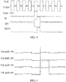
- FIG 3 shows a schematic view showing the output waveform of the 31 st GOA unit of a preferred embodiment of the GOA circuit of the present invention.
- the output signal is excellent.
- the following uses the 31 st stage GOA unit (G31) as an example to describe the operation of the circuit.
- the present invention introduces two VGL lines, wherein VGL2>VGL1 so that Vgs ⁇ 0 to reduce the risk of current leakage when the threshold voltages Vth of TFT T31, T41, T43, and T6 have negative value. Moreover, in the 168 ms voltage level maintenance duration, the node Q voltage level is not reduced, which shows that the circuit can effectively solve the Q node voltage level maintenance problem.
- FIG 4 is a schematic view showing the effect of preventing threshold voltage Vth offset for a preferred embodiment of the GOA circuit of the present invention.
- the present invention reduces the risk of current leakage when the threshold voltages Vth of TFT T31, T41, T43, and T6 have negative value. Therefore, the present invention can also prevent the Vth becomes negative.
- the circuit can still operate normally, and G(n) waveform maintains normal output.
- the capability to maintain the node Q voltage level is the key factor of restricting the outputting wide bandwidth pulses by IGZO GOA circuit.
- the present invention provides an IGZO-GOA circuit, which is able to maintain node Q voltage level, realize wide bandwidth pulse signal output, and is applicable to LCD display as well as OLED display.
- the GOA circuit of the invention can maintain node Q voltage level, realize wide bandwidth pulse signal output.
Landscapes
- Engineering & Computer Science (AREA)
- Microelectronics & Electronic Packaging (AREA)
- Theoretical Computer Science (AREA)
- Physics & Mathematics (AREA)
- Computer Hardware Design (AREA)
- General Physics & Mathematics (AREA)
- Power Engineering (AREA)
- Chemical & Material Sciences (AREA)
- Crystallography & Structural Chemistry (AREA)
- Control Of Indicators Other Than Cathode Ray Tubes (AREA)
- Shift Register Type Memory (AREA)
- Control Of El Displays (AREA)
- Thin Film Transistor (AREA)
- Liquid Crystal Display Device Control (AREA)
Abstract
Description
- The present invention relates to the field of display techniques, and in particular to a GOA circuit.
- The liquid crystal display (LCD), or LCD panel, provides the advantages of self-luminance, high emission efficiency, high resolution and contrast, near 180 ° viewing angle, wide operation temperature range, ability to achieve flexible display and large-area full-color display, and is heralded as the display device with most potential. The driving types of OLED can be divided, according to the driving method, into the passive matrix OLED (PMOLED) and active matrix OLED (AMOLED); wherein the AMOLED provides the advantages of pixels arranged in an array, self-luminous, and high luminous efficiency and is commonly used for high definition large-size display.
- At present, the horizontal scan lines of the AMOLED display panel are driven by an external integrated circuit (IC). The external IC can control the charging and discharging of the horizontal scan lines in a stage-by-stage manner. On the other hand, the Gate-driver- on-Array (GOA) approach integrates the gate scan driving circuit on the array substrate of the display panel to reduce the number of external IC so as to reduce the manufacturing cost and power consumption of the display panel, as well as achieve narrow border display device. Node Q in the GOA circuit is the gate node to control voltage level of the output signal. When node Q is at high voltage, the TFT is turned on and the output signal stays at high voltage. Therefore, in actual operation, the capability to maintain the voltage level of the node Q is the key to ensure the stable output for GOA circuit. In voltage level maintenance phase of the node Q, the voltage level of the node Q is difficult to maintain for extended duration, leading to GOA circuit failure, which remains a tough issue for GOA circuit design.
- The object of the present invention is to provide a GOA circuit, able to solve the problem of voltage level maintenance at the node Q.
- To achieve the above object, the present invention provides a GOA circuit, which comprises: a plurality of cascade GOA units, for an integer n, the n-th GOA unit for outputting an n-th horizontal scan signal comprising: a pull-up unit, a pull-up control unit, a propagation unit, a pull-down unit, a pull-down maintenance unit, and a bootstrap capacitor; the pull-up unit being connected to an n-th horizontal scan signal output end, a first node, a second node, and a first clock signal; the pull-up control unit being connected to the first node, the second node, a second clock signal, a third node, a current-stage cascade-propagate signal output end, and a previous-stage cascade-propagate signal output end or a start pulse; the propagate unit being connected to the first node, the current-stage cascade-propagate signal output end, and the first clock signal; the pull-down unit being connected to the n-th horizontal scan signal output end, the first node, the third node, a next-stage cascade-propagate signal output end, a first direct current (DC) low voltage, and a second DC low voltage; the pull-down maintenance unit being connected to the first node, the second node, the third node, the n-th horizontal scan signal output end, the current-stage cascade-propagate signal output end, a DC high voltage, the first DC low voltage and the second CD low voltage; the bootstrap capacitor having two ends connected respectively to the first node and the n-th horizontal scan signal output end.
- According to a preferred embodiment of the present invention, the first clock signal and the second clock signal are alternating signals with opposite phases.
- According to a preferred embodiment of the present invention, the pull-up control unit comprises:
- a first thin film transistor (TFT), having a gate connected to the second clock signal, a source and a drain connected respectively to the third node and the previous-stage cascade-propagate signal output end or start pulse;
- a second TFT, having a gate connected to the second clock signal, a source and a drain connected respectively to the third node and the first node;
- a third TFT, having a gate connected to the previous-stage cascade-propagate signal output end, a source and a drain connected respectively to the second node and the third node.
- According to a preferred embodiment of the present invention, when n=1, the source and the drain of the first TFT are connected to the third node and the start pulse respectively.
- According to a preferred embodiment of the present invention, the pull-up unit comprises:
- a fourth TFT, having a gate connected to the first node, a source and a drain connected respectively to the first clock signal and the n-th horizontal scan signal output end;
- a fifth TFT, having a gate connected to the first node, a source and a drain connected respectively to the first clock signal and the second node.
- According to a preferred embodiment of the present invention, the propagate unit comprises:
a sixth TFT, having a gate connected to the first node, a source and a drain connected respectively to the first clock signal and the current-stage cascade-propagate signal output end. - According to a preferred embodiment of the present invention, the pull-down unit comprises:
- a seventh TFT, having a gate connected to the next-stage cascade-propagate signal output end, a source and a drain connected respectively to the n-th horizontal scan signal output end and the second DC low voltage;
- an eighth TFT, having a gate connected to the next-stage cascade-propagate signal output end, a source and a drain connected respectively to the third node and the first node;
- a ninth TFT, having a gate connected to the next-stage cascade-propagate signal output end, a source and a drain connected respectively to the third node and the first DC low voltage.
- According to a preferred embodiment of the present invention, the pull-down maintenance comprises:
- a tenth TFT, having a gate connected to a fourth node, a source and a drain connected respectively to the n-th horizontal scan signal and the second DC low voltage;
- an eleventh TFT, having a gate connected to the fourth node, a source and a drain connected respectively to the first DC low voltage and the current-stage cascade-propagate signal output end;
- a twelfth TFT, having a gate connected to the fourth node, a source and a drain connected respectively to the second node and the second DC low voltage;
- a thirteenth TFT, having a gate connected to the fourth node, a source and a drain connected respectively to the third node and the first node;
- a fourteenth TFT, having a gate connected to the fourth node, a source and a drain connected respectively to the third node and the first DC low voltage;
- a fifteenth TFT, having a gate connected to the DC high voltage, a source and a drain, connected respectively to the DC high voltage and a gate of a sixteenth TFT;
- a sixteenth TFT, having a source and a drain connected respectively to the fourth node and the DC high voltage;
- a seventeenth TFT, having a gate connected to the first node, a source and a drain connected respectively to the gate of the sixteenth TFT and the first DC low voltage;
- an eighteenth TFT, having a gate connected to the first node, a source and a drain connected respectively to the fourth node and the first DC low voltage.
- According to a preferred embodiment of the present invention, the second DC low voltage is higher than the first DC low voltage.
- According to a preferred embodiment of the present invention, the GOA circuit is prepared based on Indium Gallium Zinc Oxide (IGZO) material.
- The present invention also provides a GOA circuit, which comprises: a plurality of cascade GOA units, for an integer n, the n-th GOA unit for outputting an n-th horizontal scan signal comprising: a pull-up unit, a pull-up control unit, a propagation unit, a pull-down unit, a pull-down maintenance unit, and a bootstrap capacitor; the pull-up unit being connected to an n-th horizontal scan signal output end, a first node, a second node, and a first clock signal; the pull-up control unit being connected to the first node, the second node, a second clock signal, a third node, a current-stage cascade-propagate signal output end, and a previous-stage cascade-propagate signal output end or a start pulse; the propagate unit being connected to the first node, the current-stage cascade-propagate signal output end, and the first clock signal; the pull-down unit being connected to the n-th horizontal scan signal output end, the first node, the third node, a next-stage cascade-propagate signal output end, a first direct current (DC) low voltage, and a second DC low voltage; the pull-down maintenance unit being connected to the first node, the second node, the third node, the n-th horizontal scan signal output end, the current-stage cascade-propagate signal output end, a DC high voltage, the first DC low voltage and the second CD low voltage; the bootstrap capacitor having two ends connected respectively to the first node and the n-th horizontal scan signal output end;
wherein the first clock signal and the second clock signal being alternating signals with opposite phases;
wherein the pull-up control unit comprising: - a first thin film transistor (TFT), having a gate connected to the second clock signal, a source and a drain connected respectively to the third node and the previous-stage cascade-propagate signal output end or start pulse;
- a second TFT, having a gate connected to the second clock signal, a source and a drain connected respectively to the third node and the first node;
- a third TFT, having a gate connected to the previous-stage cascade-propagate signal output end, a source and a drain connected respectively to the second node and the third node;
- wherein when n=1, the source and the drain of the first TFT being connected to the third node and the start pulse respectively;
- wherein the pull-up unit comprising:
- a fourth TFT, having a gate connected to the first node, a source and a drain connected respectively to the first clock signal and the n-th horizontal scan signal output end;
- a fifth TFT, having a gate connected to the first node, a source and a drain connected respectively to the first clock signal and the second node;
- wherein the propagate unit comprising:
a sixth TFT, having a gate connected to the first node, a source and a drain connected respectively to the first clock signal and the current-stage cascade-propagate signal output end.
- In summary, the GOA circuit of the present invention can effectively solve the Q node voltage level maintenance problem and achieve wide pulse GOA signal output.
- To make the technical solution of the embodiments according to the present invention, a brief description of the drawings that are necessary for the illustration of the embodiments will be given as follows. Apparently, the drawings described below show only example embodiments of the present invention and for those having ordinary skills in the art, other drawings may be easily obtained from these drawings without paying any creative effort. In the drawings:
-
Figure 1 is a schematic view showing a circuit of a preferred embodiment of the GOA circuit of the present invention; -
Figure 2 is a schematic view showing signal waveforms of input source of a preferred embodiment of the GOA circuit of the present invention; -
Figure 3 is a schematic view showing the output waveform of the 31st GOA unit of a preferred embodiment of the GOA circuit of the present invention; -
Figure 4 is a schematic view showing the effect of preventing threshold voltage Vth offset for a preferred embodiment of the GOA circuit of the present invention. - Referring to
Figure 1 and Figure 2 , the preferred embodiment of the present invention comprises 18 TFTs and a capacitor Cbt. The interconnection of the element is as shown inFigure 1 . CLK and CLKB are alternating current power source with opposite phases, VGH, VGL1 and VGL2 are DC power source, and STV is the start pulse trigger signal, which is for activating the first GOA unit in the cascade. The relation between specific waveform and voltage of each signal in the GOA circuit is shown in Table 1. The nodes N, Q, QB, Count(n-1), Count(n), Count(n+1), and G(n) are important nodes in the circuit.GOA signal voltage Min (volts) Max(volts) STV -10 + 30 CLK -10 + 30 CLKB -10 + 30 VGH + 30 VGL1 -10 VGL2 -6 - The other panel parameters applied to the preferred embodiment can be set as follows: for FHD, the number of scan lines is 1080, the number of clock signals (CK number) is 2, i.e., CLK and CLKB, the clock period is 336 ms, duty cycle is 50%, and STV width is 168 ms.
- The n-th GOA unit of the present invention comprises: a pull-up
unit 10, a pull-upcontrol unit 20, apropagation unit 30, a pull-downunit 40, a pull-downmaintenance unit 50, and a bootstrap capacitor Cbt. - The pull-up
unit 10 is connected to an n-th horizontal scan signal output end G(n), a first node Q, a second node K, and a first clock signal CLKB; the pull-upunit 10 is mainly responsible for transforming the clock signal into the output signal G(n), and comprises TFT T21 and T23; T21 has a gate connected to the first node Q, a source and a drain connected respectively to the first clock signal CLKB and the n-th horizontal scan signal output end G(n); T23 has a gate connected to the first node Q, a source and a drain connected respectively to the first clock signal CLKB and the second node K. - The pull-up
control unit 20 is connected to the first node Q, the second node K, a second clock signal CLK, a third node N, a current-stage cascade-propagate signal output end Cout(n), and a previous-stage cascade-propagate signal output end Cout(n-1) or a start pulse STV; the function of the pull-upcontrol unit 20 is to pull up the node Q voltage level and control the turn on of the pull-upunit 10. The pull-upcontrol unit 20 comprises: T11, having a gate connected to the second clock signal CLK, a source and a drain connected respectively to the third node N and the previous-stage cascade-propagate signal output end Cout(n-1) or start pulse STV; T12, having a gate connected to the second clock signal CLK, a source and a drain connected respectively to the third node N and the first node Q; T6, having a gate connected to the previous-stage cascade-propagate signal output end Cout(n-1), a source and a drain connected respectively to the second node K and the third node N. The T11 of the first GOA unit is connected to the STV signal. - The propagate
unit 30 is connected to the first node Q, the current-stage cascade-propagate signal output end Cout(n), and the first clock signal CLKB, and is mainly for using the Cout(n) signal as the input signal for the next-stage GOA unit and feedback signal for the previous-stage GOA unit. The propagateunit 30 mainly comprises: T22, having a gate connected to the first node Q, a source and a drain connected respectively to the first clock signal CLKB and the current-stage cascade-propagate signal output end Cout(n). - The pull-down
unit 40 is connected to the n-th horizontal scan signal output end G(n), the first node Q, the third node N, a next-stage cascade-propagate signal output end Cout(n), a first direct current (DC) low voltage VGL1, and a second DC low voltage VGL2, and is responsible for pulling down the node Q voltage level and the output signal to low voltage. The pull-downunit 40 comprises: T31, having a gate connected to the next-stage cascade-propagate signal output end Cout(n+1), a source and a drain connected respectively to the n-th horizontal scan signal output end G(n) and the second DC low voltage VGL2; T32, having a gate connected to the next-stage cascade-propagate signal output end Cout(n+1), a source and a drain connected respectively to the third node N and the first node Q; T33, having a gate connected to the next-stage cascade-propagate signal output end Cout(n+1), a source and a drain connected respectively to the third node N and the first DC low voltage VGL1. - The pull-down
maintenance unit 50 is connected to the first node Q, the second node K, the third node N, the n-th horizontal scan signal output end G(n), the current-stage cascade-propagate signal output end Cout(n), a DC high voltage VGH, the first DC low voltage VGL1 and the second CD low voltage VGL2, and is responsible for maintaining the node Q voltage level and G(n) in cut-off state. The pull-down maintenance unit 50 comprises: T41, having a gate connected to a fourth node QB, a source and a drain connected respectively to the n-th horizontal scan signal G(n) and the second DC low voltage VGL2; T42, having a gate connected to the fourth node QB, a source and a drain connected respectively to the first DC low voltage VGL1 and the current-stage cascade-propagate signal output end Cout(n); T43, having a gate connected to the fourth node QB, a source and a drain connected respectively to the second node K and the second DC low voltage VGL2; T44, having a gate connected to the fourth node QB, a source and a drain connected respectively to the third node N and the first node Q; T45, having a gate connected to the fourth node QB, a source and a drain connected respectively to the third node N the first DC low voltage VGL1; T51, having a gate connected to the DC high voltage VGH, a source and a drain connected respectively to the DC high voltage VGH and a gate of T53; T53, having a source and a drain connected respectively to the fourth node QB and the DC high voltage VGH; T52, having a gate connected to the first node Q, a source and a drain connected respectively to the gate of T53 and the first DC low voltage VGL1; T54, having a gate connected to the first node Q, a source and a drain connected respectively to the fourth node QBand the first DC low voltage VGL1. - The bootstrap capacitor Cbt has two ends connected respectively to the first node Q and the n-th horizontal scan signal output end G(n).
- Refer to
Figure 3 , which shows a schematic view showing the output waveform of the 31st GOA unit of a preferred embodiment of the GOA circuit of the present invention. By inputting the waveform shown inFigure 2 into the GOA circuit of the present invention, the output signal is excellent. The following uses the 31st stage GOA unit (G31) as an example to describe the operation of the circuit. - When Cout(30) is at high voltage and CLK is also at high voltage, T11 and T22 are turned on. The high voltage at Cout(30) reaches the node Q and Q becomes at high voltage, and T21, T22 and T23 are turned on. Because an inverter is between Q and QB, Q and QB have opposite phases. Hence, QB is at low voltage, and T41, T42, T43, T44, and T45 are all cut-off. Cout(32) is at low voltage and T31, T32, and T33 are cut-off. CLKB is at low voltage and the outputs Cout(n) and G(n) are both at low voltage.
- Then, Cout(30) and CLK are at low voltage, T11 and T22 are cut-off. AT this point, the node Q is under the effect of capacitor coupling and raised to an even higher voltage level. T31, T32, T33, T41, T42, T43, T44, and T45 are still cut-off. CLKB is at high voltage, and Cout(31) and G(31) are at high voltage. At this point, T6 is turned on, and the node N is at high voltage and the voltage level lowers the leakage current of T12, T44, and T32. It should be noted that the present invention introduces two VGL lines, wherein VGL2>VGL1 so that Vgs<0 to reduce the risk of current leakage when the threshold voltages Vth of TFT T31, T41, T43, and T6 have negative value. Moreover, in the 168 ms voltage level maintenance duration, the node Q voltage level is not reduced, which shows that the circuit can effectively solve the Q node voltage level maintenance problem.
- Then, CLK is raised to high voltage, Cout(30) becomes at low voltage and Cout(32) is at high voltage. T11, T12, T31, T32, and T33 are turned on. The node Q voltage level is pulled down. AT hits point, the node QB voltage level is pulled up to high voltage, and T41, T42, T43, T44, and T45 are all turned on. Cout (31) and G(31) are pulled down to low voltages VGL1 and VGL2 respectively.
- Refer to
Figure 4. Figure 4 is a schematic view showing the effect of preventing threshold voltage Vth offset for a preferred embodiment of the GOA circuit of the present invention. By introducing two VGL lines, with VGL2>VGL1, the present invention reduces the risk of current leakage when the threshold voltages Vth of TFT T31, T41, T43, and T6 have negative value. Therefore, the present invention can also prevent the Vth becomes negative. As shown inFigure 4 , when Vth drift towards the negative for 7V, the circuit can still operate normally, and G(n) waveform maintains normal output. - The capability to maintain the node Q voltage level is the key factor of restricting the outputting wide bandwidth pulses by IGZO GOA circuit. The present invention provides an IGZO-GOA circuit, which is able to maintain node Q voltage level, realize wide bandwidth pulse signal output, and is applicable to LCD display as well as OLED display.
- In summary, the GOA circuit of the invention can maintain node Q voltage level, realize wide bandwidth pulse signal output.
- It should be noted that in the present disclosure the terms, such as, first, second are only for distinguishing an entity or operation from another entity or operation, and does not imply any specific relation or order between the entities or operations. Also, the terms "comprises", "include", and other similar variations, do not exclude the inclusion of other non-listed elements. Without further restrictions, the expression "comprises a..." does not exclude other identical elements from presence besides the listed elements.
- Embodiments of the present invention have been described, but not intending to impose any unduly constraint to the appended claims. Any modification of equivalent structure or equivalent process made according to the disclosure and drawings of the present invention, or any application thereof, directly or indirectly, to other related fields of technique, is considered encompassed in the scope of protection defined by the clams of the present invention.
Claims (15)
- A gate-driver-on-array, GOA, circuit, which comprises: a plurality of cascade GOA units, for an integer n, the n-th GOA unit for outputting an n-th horizontal scan signal comprising: a pull-up unit, a pull-up control unit, a propagation unit, a pull-down unit, a pull-down maintenance unit, and a bootstrap capacitor; the pull-up unit being connected to an n-th horizontal scan signal output end, a first node, a second node, and a first clock signal; the pull-up control unit being connected to the first node, the second node, a second clock signal, a third node, a current-stage cascade-propagate signal output end, and a previous-stage cascade-propagate signal output end or a start pulse; the propagate unit being connected to the first node, the current-stage cascade-propagate signal output end, and the first clock signal; the pull-down unit being connected to the n-th horizontal scan signal output end, the first node, the third node, a next-stage cascade-propagate signal output end, a first direct current, DC, low voltage, and a second DC low voltage; the pull-down maintenance unit being connected to the first node, the second node, the third node, the n-th horizontal scan signal output end, the current-stage cascade-propagate signal output end, a DC high voltage, the first DC low voltage and the second CD low voltage; the bootstrap capacitor having two ends connected respectively to the first node and the n-th horizontal scan signal output end.
- The GOA circuit as claimed in Claim 1, wherein the first clock signal and the second clock signal are alternating signals with opposite phases.
- The GOA circuit as claimed in Claim 1, wherein the pull-up control unit comprises:a first thin film transistor, TFT, having a gate connected to the second clock signal, a source and a drain connected respectively to the third node and the previous-stage cascade-propagate signal output end or start pulse;a second TFT, having a gate connected to the second clock signal, a source and a drain connected respectively to the third node and the first node;a third TFT, having a gate connected to the previous-stage cascade-propagate signal output end, a source and a drain connected respectively to the second node and the third node.
- The GOA circuit as claimed in Claim 3, wherein when n=1, the source and the drain of the first TFT are connected to the third node and the start pulse respectively.
- The GOA circuit as claimed in Claim 1, wherein the pull-up unit comprises:a fourth TFT, having a gate connected to the first node, a source and a drain connected respectively to the first clock signal and the n-th horizontal scan signal output end;a fifth TFT, having a gate connected to the first node, a source and a drain connected respectively to the first clock signal and the second node.
- The GOA circuit as claimed in Claim 1, wherein the propagation unit comprises:
a sixth TFT, having a gate connected to the first node, a source and a drain connected respectively to the first clock signal and the current-stage cascade-propagate signal output end. - The GOA circuit as claimed in Claim 1, wherein the pull-down unit comprises:a seventh TFT, having a gate connected to the next-stage cascade-propagate signal output end, a source and a drain connected respectively to the n-th horizontal scan signal output end and the second DC low voltage;an eighth TFT, having a gate connected to the next-stage cascade-propagate signal output end, a source and a drain connected respectively to the third node and the first node;a ninth TFT, having a gate connected to the next-stage cascade-propagate signal output end, a source and a drain connected respectively to the third node and the first DC low voltage.
- The GOA circuit as claimed in Claim 1, wherein the pull-down maintenance unit comprises:a tenth TFT, having a gate connected to a fourth node, a source and a drain connected respectively to the n-th horizontal scan signal and the second DC low voltage;an eleventh TFT, having a gate connected to the fourth node, a source and a drain connected respectively to the first DC low voltage and the current-stage cascade-propagate signal output end;a twelfth TFT, having a gate connected to the fourth node, a source and a drain connected respectively to the second node and the second DC low voltage;a thirteenth TFT, having a gate connected to the fourth node, a source and a drain connected respectively to the third node and the first node;a fourteenth TFT, having a gate connected to the fourth node, a source and a drain connected respectively to the third node and the first DC low voltage;a fifteenth TFT, having a gate connected to the DC high voltage, a source and a drain connected respectively to the DC high voltage and a gate of a sixteenth TFT;the sixteenth TFT, having a source and a drain connected respectively to the fourth node and the DC high voltage;a seventeenth TFT, having a gate connected to the first node, a source and a drain connected respectively to the gate of the sixteenth TFT and the first DC low voltage;an eighteenth TFT, having a gate connected to the first node, a source and a drain connected respectively to the fourth node and the first DC low voltage.
- The GOA circuit as claimed in Claim 1, wherein the second DC low voltage is higher than the first DC low voltage.
- The GOA circuit as claimed in Claim 1, wherein the GOA circuit is prepared based on Indium Gallium Zinc Oxide, IGZO, material.
- A gate-driver-on-array, GOA, circuit, which comprises: a plurality of cascade GOA units, for an integer n, the n-th GOA unit for outputting an n-th horizontal scan signal comprising: a pull-up unit, a pull-up control unit, a propagation unit, a pull-down unit, a pull-down maintenance unit, and a bootstrap capacitor; the pull-up unit being connected to an n-th horizontal scan signal output end, a first node, a second node, and a first clock signal; the pull-up control unit being connected to the first node, the second node, a second clock signal, a third node, a current-stage cascade-propagate signal output end, and a previous-stage cascade-propagate signal output end or a start pulse; the propagate unit being connected to the first node, the current-stage cascade-propagate signal output end, and the first clock signal; the pull-down unit being connected to the n-th horizontal scan signal output end, the first node, the third node, a next-stage cascade-propagate signal output end, a first direct current, DC, low voltage, and a second DC low voltage; the pull-down maintenance unit being connected to the first node, the second node, the third node, the n-th horizontal scan signal output end, the current-stage cascade-propagate signal output end, a DC high voltage, the first DC low voltage and the second CD low voltage; the bootstrap capacitor having two ends connected respectively to the first node and the n-th horizontal scan signal output end;
wherein the first clock signal and the second clock signal being alternating signals with opposite phases;
the pull-up control unit comprising:a first thin film transistor, TFT, having a gate connected to the second clock signal, a source and a drain connected respectively to the third node and the previous-stage cascade-propagate signal output end or start pulse;a second TFT, having a gate connected to the second clock signal, a source and a drain connected respectively to the third node and the first node;a third TFT, having a gate connected to the previous-stage cascade-propagate signal output end, a source and a drain connected respectively to the second node and the third node;wherein when n=1, the source and the drain of the first TFT being connected to the third node and the start pulse respectively;wherein the pull-up unit comprising:a fourth TFT, having a gate connected to the first node, a source and a drain connected respectively to the first clock signal and the n-th horizontal scan signal output end;a fifth TFT, having a gate connected to the first node, a source and a drain connected respectively to the first clock signal and the second node;wherein the propagation unit comprising:
a sixth TFT, having a gate connected to the first node, a source and a drain connected respectively to the first clock signal and the current-stage cascade-propagate signal output end. - The GOA circuit as claimed in Claim 11, wherein the pull-down unit comprises:a seventh TFT, having a gate connected to the next-stage cascade-propagate signal output end, a source and a drain connected respectively to the n-th horizontal scan signal output end and the second DC low voltage;an eighth TFT, having a gate connected to the next-stage cascade-propagate signal output end, a source and a drain connected respectively to the third node and the first node;a ninth TFT, having a gate connected to the next-stage cascade-propagate signal output end, a source and a drain connected respectively to the third node and the first DC low voltage.
- The GOA circuit as claimed in Claim 11, wherein the pull-down maintenance unit comprises:a tenth TFT, having a gate connected to a fourth node, a source and a drain connected respectively to the n-th horizontal scan signal and the second DC low voltage;an eleventh TFT, having a gate connected to the fourth node, a source and a drain connected respectively to the first DC low voltage and the current-stage cascade-propagate signal output end;a twelfth TFT, having a gate connected to the fourth node, a source and a drain connected respectively to the second node and the second DC low voltage;a thirteenth TFT, having a gate connected to the fourth node, a source and a drain connected respectively to the third node and the first node;a fourteenth TFT, having a gate connected to the fourth node, a source and a drain connected respectively to the third node and the first DC low voltage;a fifteenth TFT, having a gate connected to the DC high voltage, a source and a drain connected respectively to the DC high voltage and a gate of a sixteenth TFT;the sixteenth TFT, having a source and a drain connected respectively to the fourth node and the DC high voltage;a seventeenth TFT, having a gate connected to the first node, a source and a drain connected respectively to the gate of the sixteenth TFT and the first DC low voltage;an eighteenth TFT, having a gate connected to the first node, a source and a drain connected respectively to the fourth node and the first DC low voltage.
- The GOA circuit as claimed in Claim 11, wherein the second DC low voltage is higher than the first DC low voltage.
- The GOA circuit as claimed in Claim 11, wherein the GOA circuit is prepared based on Indium Gallium Zinc Oxide, IGZO, material.
Applications Claiming Priority (2)
| Application Number | Priority Date | Filing Date | Title |
|---|---|---|---|
| CN201710745219.8A CN107393473B (en) | 2017-08-25 | 2017-08-25 | GOA circuit |
| PCT/CN2017/111330 WO2019037299A1 (en) | 2017-08-25 | 2017-11-16 | Goa circuit |
Publications (2)
| Publication Number | Publication Date |
|---|---|
| EP3675114A1 true EP3675114A1 (en) | 2020-07-01 |
| EP3675114A4 EP3675114A4 (en) | 2021-01-27 |
Family
ID=60345403
Family Applications (1)
| Application Number | Title | Priority Date | Filing Date |
|---|---|---|---|
| EP17922764.0A Withdrawn EP3675114A4 (en) | 2017-08-25 | 2017-11-16 | GOA CIRCUIT |
Country Status (6)
| Country | Link |
|---|---|
| US (1) | US10446085B2 (en) |
| EP (1) | EP3675114A4 (en) |
| JP (1) | JP6794579B2 (en) |
| KR (1) | KR102222927B1 (en) |
| CN (1) | CN107393473B (en) |
| WO (1) | WO2019037299A1 (en) |
Families Citing this family (46)
| Publication number | Priority date | Publication date | Assignee | Title |
|---|---|---|---|---|
| CN108182917B (en) * | 2018-01-02 | 2020-07-07 | 京东方科技集团股份有限公司 | Shift register, driving method thereof and grid driving circuit |
| CN108564914B (en) * | 2018-04-24 | 2021-08-17 | 京东方科技集团股份有限公司 | Shift register unit, driving method, gate driving circuit and display device |
| CN109003584B (en) * | 2018-07-24 | 2020-06-26 | 惠科股份有限公司 | Display device and display panel thereof |
| CN110068970B (en) * | 2019-04-18 | 2020-09-11 | 深圳市华星光电半导体显示技术有限公司 | TFT array substrate and display panel |
| CN110111715B (en) * | 2019-04-22 | 2023-02-28 | 深圳市华星光电半导体显示技术有限公司 | GOA circuit and display panel |
| CN109935192B (en) * | 2019-04-22 | 2022-04-26 | 深圳市华星光电半导体显示技术有限公司 | GOA circuit and display panel |
| CN110060639B (en) * | 2019-04-24 | 2021-07-06 | 深圳市华星光电半导体显示技术有限公司 | Array substrate |
| CN110047438B (en) * | 2019-04-29 | 2020-09-01 | 深圳市华星光电技术有限公司 | GOA circuit |
| CN109961737A (en) * | 2019-05-05 | 2019-07-02 | 深圳市华星光电半导体显示技术有限公司 | GOA circuit and display device |
| CN109961746B (en) * | 2019-05-06 | 2020-09-08 | 深圳市华星光电半导体显示技术有限公司 | drive circuit for display |
| CN110111743B (en) * | 2019-05-07 | 2020-11-24 | 深圳市华星光电半导体显示技术有限公司 | GOA circuit and display panel |
| CN110223648B (en) * | 2019-05-09 | 2020-07-10 | 深圳市华星光电半导体显示技术有限公司 | Driving circuit for display screen |
| CN110136652B (en) * | 2019-05-24 | 2020-10-16 | 深圳市华星光电半导体显示技术有限公司 | GOA circuit and array substrate |
| CN110415648A (en) * | 2019-07-16 | 2019-11-05 | 深圳市华星光电半导体显示技术有限公司 | GOA circuit |
| CN110390918A (en) * | 2019-07-18 | 2019-10-29 | 深圳市华星光电半导体显示技术有限公司 | Tft array substrate and display panel |
| CN110299112B (en) * | 2019-07-18 | 2020-09-01 | 深圳市华星光电半导体显示技术有限公司 | GOA circuit |
| CN110379349B (en) * | 2019-07-22 | 2020-10-16 | 深圳市华星光电半导体显示技术有限公司 | Gate drive circuit |
| CN110675793A (en) * | 2019-09-05 | 2020-01-10 | 深圳市华星光电半导体显示技术有限公司 | Display driving circuit |
| CN110675828A (en) * | 2019-09-10 | 2020-01-10 | 深圳市华星光电半导体显示技术有限公司 | GOA circuit |
| CN110767190B (en) | 2019-10-14 | 2021-09-24 | 深圳市华星光电半导体显示技术有限公司 | GOA circuit |
| CN113066422B (en) * | 2019-12-13 | 2022-06-24 | 华为机器有限公司 | Scanning and lighting driving circuit, scanning and lighting driving system, display panel |
| CN111223433B (en) * | 2020-01-19 | 2021-01-15 | 深圳市华星光电半导体显示技术有限公司 | GOA circuit and display device |
| CN111261108A (en) * | 2020-02-11 | 2020-06-09 | 深圳市华星光电半导体显示技术有限公司 | Gate drive circuit |
| CN111199703B (en) * | 2020-02-28 | 2021-07-06 | 深圳市华星光电半导体显示技术有限公司 | GOA circuit and display panel |
| CN113496681A (en) | 2020-03-18 | 2021-10-12 | Tcl华星光电技术有限公司 | GOA circuit and display panel |
| US10950155B1 (en) * | 2020-03-27 | 2021-03-16 | Shenzhen China Star Optoelectronics Semiconductor Display Technology Co., Ltd. | GOA circuit and display panel |
| CN111402829B (en) * | 2020-04-10 | 2021-07-27 | 苏州华星光电技术有限公司 | GOA circuit and display panel |
| CN111986624B (en) * | 2020-08-04 | 2022-02-08 | 邵阳学院 | Low-oscillation GOA circuit |
| CN112233628B (en) * | 2020-08-13 | 2022-04-26 | 深圳市华星光电半导体显示技术有限公司 | GOA circuit and liquid crystal display |
| CN111986605B (en) * | 2020-08-13 | 2022-05-31 | 深圳市华星光电半导体显示技术有限公司 | Gate drive circuit |
| CN112259033A (en) * | 2020-10-16 | 2021-01-22 | 深圳市华星光电半导体显示技术有限公司 | Array substrate row driving circuit and display device |
| CN112365855B (en) * | 2020-11-04 | 2022-11-08 | 深圳市华星光电半导体显示技术有限公司 | GOA circuit and liquid crystal display |
| KR102888981B1 (en) | 2020-11-12 | 2025-11-24 | 삼성디스플레이 주식회사 | Display device and method of operating a display device |
| KR102763920B1 (en) * | 2021-07-08 | 2025-02-07 | 엘지디스플레이 주식회사 | Inverter circuit, gate driver using the same ane sensing method display device |
| CN113689824B (en) * | 2021-09-06 | 2022-12-23 | 深圳市华星光电半导体显示技术有限公司 | Emission control driver and display device |
| CN115775539A (en) * | 2021-09-07 | 2023-03-10 | 深圳市柔宇科技股份有限公司 | GOA circuit, display panel and electronic device |
| CN114203112B (en) * | 2021-12-29 | 2023-07-25 | 深圳市华星光电半导体显示技术有限公司 | GOA circuit, display panel and display device |
| CN114842786B (en) * | 2022-04-26 | 2024-08-16 | Tcl华星光电技术有限公司 | GOA circuit and display panel |
| JP2025539285A (en) | 2022-12-19 | 2025-12-05 | 京東方科技集團股▲ふん▼有限公司 | Driving circuit, driving method, driving module and display device |
| US12322343B2 (en) | 2022-12-19 | 2025-06-03 | Chengdu Boe Optoelectronics Technology Co., Ltd. | Driving circuit, driving method, driving module and display device |
| WO2024130493A1 (en) | 2022-12-19 | 2024-06-27 | 京东方科技集团股份有限公司 | Driving circuit, driving method, driving module and display apparatus |
| WO2024130491A1 (en) | 2022-12-19 | 2024-06-27 | 京东方科技集团股份有限公司 | Driving circuit, driving method, driving module, and display device |
| CN118871974B (en) | 2022-12-19 | 2026-01-02 | 京东方科技集团股份有限公司 | Drive circuit, drive method, drive module and display device |
| CN116665575B (en) * | 2023-04-18 | 2025-10-21 | 惠科股份有限公司 | Row scanning unit, row scanning cascade circuit and driving method |
| CN116453443B (en) * | 2023-04-19 | 2025-07-11 | 重庆邮电大学 | GOA circuit, GOA unit and driving method thereof, and array substrate |
| CN118038833B (en) * | 2024-03-29 | 2024-12-24 | 绵阳惠科光电科技有限公司 | Scan driving circuit, scan driving method, display panel and display device |
Family Cites Families (16)
| Publication number | Priority date | Publication date | Assignee | Title |
|---|---|---|---|---|
| US5859630A (en) * | 1996-12-09 | 1999-01-12 | Thomson Multimedia S.A. | Bi-directional shift register |
| US8174478B2 (en) * | 2006-06-12 | 2012-05-08 | Samsung Electronics Co., Ltd. | Gate driving circuit and display apparatus having the same |
| KR101277152B1 (en) * | 2006-08-24 | 2013-06-21 | 삼성디스플레이 주식회사 | Gate driving circuit and display device having the same |
| JP5116277B2 (en) * | 2006-09-29 | 2013-01-09 | 株式会社半導体エネルギー研究所 | Semiconductor device, display device, liquid crystal display device, display module, and electronic apparatus |
| KR101478667B1 (en) * | 2008-10-16 | 2015-01-02 | 삼성디스플레이 주식회사 | Display and driving method of the same |
| KR102024116B1 (en) * | 2012-03-22 | 2019-11-15 | 삼성디스플레이 주식회사 | A gate driving circuit and a display apparatus using the same |
| KR20150069317A (en) * | 2013-12-13 | 2015-06-23 | 한국전자통신연구원 | Gate driver circuit outputs overlapped pulses |
| CN103680388B (en) * | 2013-12-26 | 2015-11-11 | 深圳市华星光电技术有限公司 | For recoverable GOA circuit and the display device of flat pannel display |
| CN103745700B (en) * | 2013-12-27 | 2015-10-07 | 深圳市华星光电技术有限公司 | Self-repair type gate driver circuit |
| CN103730094B (en) * | 2013-12-30 | 2016-02-24 | 深圳市华星光电技术有限公司 | Goa circuit structure |
| CN104575420B (en) * | 2014-12-19 | 2017-01-11 | 深圳市华星光电技术有限公司 | Scan driving circuit |
| CN105427786B (en) * | 2015-11-19 | 2018-03-20 | 北京大学深圳研究生院 | A kind of gate drive circuit unit and gate driving circuit |
| CN106652936B (en) * | 2016-12-09 | 2019-10-22 | 深圳市华星光电技术有限公司 | GOA circuit and display device |
| CN106683631B (en) * | 2016-12-30 | 2018-06-22 | 深圳市华星光电技术有限公司 | The GOA circuits and display device of a kind of IGZO thin film transistor (TFT)s |
| CN106710503B (en) * | 2016-12-30 | 2019-11-22 | 深圳市华星光电技术有限公司 | Scan driving circuit and display device |
| CN106898290B (en) * | 2017-04-21 | 2019-08-02 | 深圳市华星光电半导体显示技术有限公司 | scan drive circuit |
-
2017
- 2017-08-25 CN CN201710745219.8A patent/CN107393473B/en not_active Expired - Fee Related
- 2017-11-16 KR KR1020207007779A patent/KR102222927B1/en not_active Expired - Fee Related
- 2017-11-16 EP EP17922764.0A patent/EP3675114A4/en not_active Withdrawn
- 2017-11-16 WO PCT/CN2017/111330 patent/WO2019037299A1/en not_active Ceased
- 2017-11-16 US US15/579,947 patent/US10446085B2/en not_active Expired - Fee Related
- 2017-11-16 JP JP2020506328A patent/JP6794579B2/en not_active Expired - Fee Related
Also Published As
| Publication number | Publication date |
|---|---|
| KR102222927B1 (en) | 2021-03-05 |
| US20190066596A1 (en) | 2019-02-28 |
| KR20200037404A (en) | 2020-04-08 |
| JP2020530132A (en) | 2020-10-15 |
| JP6794579B2 (en) | 2020-12-02 |
| WO2019037299A1 (en) | 2019-02-28 |
| CN107393473A (en) | 2017-11-24 |
| EP3675114A4 (en) | 2021-01-27 |
| CN107393473B (en) | 2018-11-23 |
| US10446085B2 (en) | 2019-10-15 |
Similar Documents
| Publication | Publication Date | Title |
|---|---|---|
| US10446085B2 (en) | GOA circuit for solving problem of voltage level maintenance at the node Q | |
| USRE49782E1 (en) | Shift register and driving method thereof gate driving circuit and display apparatus | |
| US9570026B2 (en) | Scan driving circuit and LCD device | |
| CN110299112B (en) | GOA circuit | |
| US10347351B2 (en) | Display device and method of driving the same | |
| US9071230B2 (en) | Gate driving circuit and display apparatus having the same | |
| KR102174888B1 (en) | Gate driving circuit and display device having the same | |
| US20210407356A1 (en) | Goa circuit and display device | |
| US9741301B2 (en) | Driving circuit of display panel, display device, and method for driving the driving circuit of the display panel | |
| US11107381B2 (en) | Shift register and method for driving the same, gate driving circuit and display device | |
| CN102419949B (en) | Shift register circuit | |
| US10714041B2 (en) | Gate driver on array circuit | |
| US20160284303A1 (en) | Scan driving circuit and lcd device | |
| WO2020224154A1 (en) | Goa circuit and display device | |
| US11393402B2 (en) | OR logic operation circuit and driving method, shift register unit, gate drive circuit, and display device | |
| CN110148382B (en) | GOA circuit, display panel and display device | |
| WO2021012313A1 (en) | Gate driving circuit | |
| CN110060639B (en) | Array substrate | |
| WO2020224133A1 (en) | Goa circuit, display panel and display apparatus | |
| EP3564941A1 (en) | Goa circuit | |
| CN104505013A (en) | Driving circuit | |
| US10565935B2 (en) | Scan driving circuit for OLED and display panel | |
| US20210335217A1 (en) | Gate on array unit, goa circuit and display panel | |
| KR101721260B1 (en) | Level shifter and liquid crystal display using the same | |
| CN115762421A (en) | GOA circuit and display panel |
Legal Events
| Date | Code | Title | Description |
|---|---|---|---|
| STAA | Information on the status of an ep patent application or granted ep patent |
Free format text: STATUS: THE INTERNATIONAL PUBLICATION HAS BEEN MADE |
|
| PUAI | Public reference made under article 153(3) epc to a published international application that has entered the european phase |
Free format text: ORIGINAL CODE: 0009012 |
|
| STAA | Information on the status of an ep patent application or granted ep patent |
Free format text: STATUS: REQUEST FOR EXAMINATION WAS MADE |
|
| 17P | Request for examination filed |
Effective date: 20200313 |
|
| AK | Designated contracting states |
Kind code of ref document: A1 Designated state(s): AL AT BE BG CH CY CZ DE DK EE ES FI FR GB GR HR HU IE IS IT LI LT LU LV MC MK MT NL NO PL PT RO RS SE SI SK SM TR |
|
| AX | Request for extension of the european patent |
Extension state: BA ME |
|
| DAV | Request for validation of the european patent (deleted) | ||
| DAX | Request for extension of the european patent (deleted) | ||
| A4 | Supplementary search report drawn up and despatched |
Effective date: 20210114 |
|
| RIC1 | Information provided on ipc code assigned before grant |
Ipc: G09G 3/36 20060101AFI20201223BHEP Ipc: G09G 3/3266 20160101ALI20201223BHEP |
|
| STAA | Information on the status of an ep patent application or granted ep patent |
Free format text: STATUS: EXAMINATION IS IN PROGRESS |
|
| 17Q | First examination report despatched |
Effective date: 20221215 |
|
| STAA | Information on the status of an ep patent application or granted ep patent |
Free format text: STATUS: THE APPLICATION IS DEEMED TO BE WITHDRAWN |
|
| 18D | Application deemed to be withdrawn |
Effective date: 20230228 |