EP3674844B1 - Schaltung und betriebsverfahren für eine adaptive ladungsratenenergieversorgung - Google Patents
Schaltung und betriebsverfahren für eine adaptive ladungsratenenergieversorgung Download PDFInfo
- Publication number
- EP3674844B1 EP3674844B1 EP20158210.3A EP20158210A EP3674844B1 EP 3674844 B1 EP3674844 B1 EP 3674844B1 EP 20158210 A EP20158210 A EP 20158210A EP 3674844 B1 EP3674844 B1 EP 3674844B1
- Authority
- EP
- European Patent Office
- Prior art keywords
- comparator
- battery
- current
- voltage
- battery charger
- Prior art date
- Legal status (The legal status is an assumption and is not a legal conclusion. Google has not performed a legal analysis and makes no representation as to the accuracy of the status listed.)
- Expired - Lifetime
Links
Images
Classifications
-
- G—PHYSICS
- G06—COMPUTING OR CALCULATING; COUNTING
- G06F—ELECTRIC DIGITAL DATA PROCESSING
- G06F1/00—Details not covered by groups G06F3/00 - G06F13/00 and G06F21/00
- G06F1/26—Power supply means, e.g. regulation thereof
- G06F1/266—Arrangements to supply power to external peripherals either directly from the computer or under computer control, e.g. supply of power through the communication port, computer controlled power-strips
-
- H—ELECTRICITY
- H02—GENERATION; CONVERSION OR DISTRIBUTION OF ELECTRIC POWER
- H02J—CIRCUIT ARRANGEMENTS OR SYSTEMS FOR SUPPLYING OR DISTRIBUTING ELECTRIC POWER; SYSTEMS FOR STORING ELECTRIC ENERGY
- H02J7/00—Circuit arrangements for charging or depolarising batteries or for supplying loads from batteries
-
- H02J7/92—
-
- H02J7/927—
-
- H02J7/96—
-
- H—ELECTRICITY
- H02—GENERATION; CONVERSION OR DISTRIBUTION OF ELECTRIC POWER
- H02J—CIRCUIT ARRANGEMENTS OR SYSTEMS FOR SUPPLYING OR DISTRIBUTING ELECTRIC POWER; SYSTEMS FOR STORING ELECTRIC ENERGY
- H02J2207/00—Indexing scheme relating to details of circuit arrangements for charging or depolarising batteries or for supplying loads from batteries
- H02J2207/30—Charge provided using DC bus or data bus of a computer
-
- H—ELECTRICITY
- H02—GENERATION; CONVERSION OR DISTRIBUTION OF ELECTRIC POWER
- H02J—CIRCUIT ARRANGEMENTS OR SYSTEMS FOR SUPPLYING OR DISTRIBUTING ELECTRIC POWER; SYSTEMS FOR STORING ELECTRIC ENERGY
- H02J2207/00—Indexing scheme relating to details of circuit arrangements for charging or depolarising batteries or for supplying loads from batteries
- H02J2207/40—Indexing scheme relating to details of circuit arrangements for charging or depolarising batteries or for supplying loads from batteries adapted for charging from various sources, e.g. AC, DC or multivoltage
Definitions
- This invention relates in general to battery chargers, and more specifically to a method and apparatus for charging a battery in a portable communication device from a variety of power sources, including limited capacity sources such as an integral power node of a computer data bus.
- power sources including limited capacity sources such as an integral power node of a computer data bus.
- One such computer data bus would be a USB (universal serial bus) port.
- Battery chargers generally receive power from a standard AC electrical outlet and convert the AC power into a low DC voltage for recharging a battery.
- the battery chargers of these portable devices also generally employ a "battery charge controller" to manage the charging of the battery.
- battery charge controllers offer functionality such as:
- USB universal serial bus
- USB ports are designed to support data communication at speeds of 12 megabits and 1.5 megabits per second (USB 2.0 provides for up to 480 megabits per second), support PnP (Plug and Play) installation software, and support hot plugging (i.e. devices can be connected and disconnected while the PC is running).
- USB ports are often used as interfaces to connect keyboards, mouses, game controllers, printers and scanners to PCs.
- USB ports are able to supply limited power to a connected device.
- the standard USB specification requires that "high-power" USB ports be operable to provide a supply voltage of 4.75 - 5.25 VDC and supply a maximum current of at least 500mA (five units).
- the specification for "low-power” USB ports requires a supply voltage of 4.40 - 5.25 VDC and current of 100 mA (one unit).
- USB ports would seem to be a very logical choice as a power supply for portable devices for a number of reasons.
- USB ports supply a low DC voltage supply which is often very close to, or just above, the voltage of the battery being charged (many portable devices having battery voltages in the range of 2.5 - 4.5 VDC).
- many portable devices may be operable to upload and download data or software, to and from a personal computer or a laptop computer (often referred to as "syncing").
- many portable devices are supplied with docking cradles as shown in the system diagram of Figure 1 . This is quite a straightforward system, as the docking cradle 10 is connected to a USB port 12 of a personal computer (PC) 14, via a simple USB cable and connectors 16.
- the mobile device 18 need only be placed into the docking cradle 10 and an electronic connection to the (PC) 14, is made.
- USB port 12 If the USB port 12 has sufficient power, it makes much more sense to use the USB port 12 to supply charging power to the mobile device 18, rather than using a separate AC charger. For example:
- USB USB standard
- the USB standard is widely accepted, so that a traveller whose mobile device is equipped with a USB connector will have a much greater chance of finding a charging source.
- USB ports can only provide limited power, while typical battery charge controllers are designed to receive a steady, high capacity power supply (that is, the input voltage at the battery charge controller is at or near its designed value, and does not drop as charging current increases).
- the problem becomes clear when considering the block diagram of Figure 2 .
- the components of Figure 2 are the same as those of Figure 1 , specifically, a docking cradle 10 powered from a USB port 12 of a PC 14, via cable and connectors 16, and feeding a portable device 18 resting in the cradle 10. From this presentation, it is clear that the voltage output from the USB port 12, V USB , will drop as it crosses the cable and connectors 16, due to its resistance, R CABLE .
- LTC 4053-4.2 USB Compatible Lithium-Ion Battery Charger with thermal Regulation discloses a linear charger for lithium-ion batteries that can be powered directly from a USB port.
- US 6300744 B1 discloses an AC adapter to supply power to both an electronic device and a rechargeable battery.
- the voltage at the output terminal of the AC adapter is detected and delivered to a battery charger that is used to supply a constant current to the battery, when the computer is turned on while the battery is being recharged.
- a voltage detector instructs the battery charger to limit the current delivered to the battery, and the current is reduced until the voltage at the output of the AC adapter again reaches the trigger voltage.
- the present invention provides a battery charger as detailed in claim 1. Advantageous features are provided in the dependent claims..
- the general problem addressed by the invention is that typical battery charge controllers are designed to receive a steady, high capacity power supply while such a power supply is often unavailable, or is simply inconvenient.
- One of the most common battery charge controllers for example, the LTC1734 from Linear Technology is designed to receive 5 VDC in, and has a low voltage lockout at 4.53V (that is, if the LTC1734 receives a supply voltage of less than 4.53VDC, it simply shuts down).
- the voltage drop across the supply cable and connectors 16 are considered, the voltage supplied by the power node of a data bus such as a USB port, may be lower than this low voltage lockout. Therefore, though the LTC1734 is widely available, inexpensive and reliable, it cannot be used effectively in this environment.
- FIG. 3 A circuit which overcomes this problem, is presented as a block diagram in Figure 3 .
- This figure presents a battery charging circuit which uses a standard battery charge controller 30 known in the art, coupled to a rechargeable battery or batteries 32.
- the battery charge controller 30 is provided with power from some manner of external power, such as a computer data bus.
- This power connection is presented in Figure 3 in the form of input voltage V BUS .
- This V BUS voltage will be reduced due to the resistance of the electrical cable and connectors 16, R CABLE .
- the voltage drop across R CABLE may result in the V CHRG voltage being lower than the low voltage threshold for the battery charge controller 30.
- the invention therefore adds a current regulator 34 to the circuit.
- the resistance R CABLE is of course fixed, but by reducing the current drawn by the battery charge controller 30, I CABLE , the voltage drop across R CABLE will decrease, thus avoiding the low voltage shut off of the battery charge controller 30, and allowing the battery 32 to be charged.
- the current regulator 34 uses V CHRG as an input (via connection 36 ), while in other embodiments the current regulator 34 uses an output of the battery charge controller 30 (via connector 38 ). Still other embodiments use no feedback to the current regulator 34.
- V CHRG may effectively be in the range of 4.37 VDC; well below the 4.53 VDC cut off for the LTC1734 battery charge controller.
- Equation (1) can also be used to determine a current level, I CABLE , which does not cause the battery charge controller 30 to shutdown:
- the current I CABLE may have to be reduced to 0.18 A to avoid the low voltage shutdown.
- circuit in Figure 3 allows computer data buses and similar power supplies with limited capacity, to be used to charge mobile devices, without causing the battery charge controller 30 to shut down.
- the solution of this embodiment adapts to the capabilities of any external power source to minimize charge time. If, for example, 5 VDC arrives at the input of the battery charge controller 30 with unlimited current and no voltage drop as the current draw. increases, then the regulating circuit 34 will not restrict the current drawn.
- Figure 4 presents an electrical schematic diagram charging circuit which employs two main components: a comparator 50 and a LTC1734 battery charge controller 52 having a current control pin PROG. Varying the current drawn through the control pin PROG will vary the current supplied by the LTC1734 battery charge controller 52 to the battery 32. Drawing more current out of the PROG pin will increase the charge current, while reducing the PROG current will reduce the charge current.
- the LTC1734 controller can be operated in either constant current mode, or constant voltage mode.
- the LTC1734 controller 52 In the constant voltage mode (entered when the charge voltage of the battery 32 reaches 4.2 VDC externally), the LTC1734 controller 52 servos its DRIVE pin to maintain its BAT pin at 4.2 VDC. In this mode, the current provided by the LTC1734 controller 52 will necessarily drop, and the current flowing out of the PROG pin will drop accordingly. As this latter mode of operation is not affected by the system described herein, it will not be discussed in any further detail.
- the minimum required voltage at VCC for proper operation of the LTC1734 controller 52 is 4.53 VDC, and the USB specification states that for standard USB equipment under a high load (i.e. 500mA), V CHRG may be pulled as low as 4.35V - too low for the LTC1734 controller 52 to operate.
- the comparator 50 monitors V CHRG (scaled down to a more useful voltage - V N - by the voltage divider R1 and R2) fed to the inverting input of the comparator 50 and compares it to a reference voltage (V P ) which is fed to the comparator 50's non- inverting input.
- R5 also serves to isolate other components from the LTC1734 controller 52, ensuring proper operation of the LTC1734 controller 52.
- V C1 is controlled by the comparator 50.
- the comparator 50 is an open- drain comparator (a MAX9120 comparator was used for testing purposes, though similar parts such as the LMV7235 should work as well) when V N > V P , the comparator 50 will sink current into its output pin; otherwise the output pin will float.
- the control loop operates as follows:
- Resistor R4 smooths out the ripples on C1 and limits current transients through the comparator 50's output.
- R OUT is the resistance from the comparator 50's output to GND when the output is active. Because the LTC1734 controller 52 is susceptible to malfunction due to capacitive effects in the PROG circuit, it is best to keep R4 ⁇ 0.1 R3, but this will depend on the application, and can easily be determined by one skilled in the art.
- V C1 0 and the charger will start and stay on.
- a high-on-reset signal of 3.0V applied to CHG_CTRL will keep the charger off; once the "off' state has been established, the CHG_CTRL signal can be removed. Conversely, pulling CHG_CTRL to GND for a period of time and then floating it will turn on the charger.
- the R4, C1 time constant was chosen to be at least 10 times larger than the propagation delay of the MAX9120 for stability.
- a 1 ⁇ resistor was used to simulate the resistance of the supply cable and connectors 16.
- V BUS 6 VDC
- I CHRG 440mA
- V BUS 4.63 VDC
- V PROG 4.625 VDC
- the LTC1734 controller 52 could be turned on again by momentarily pulling CHG_CTRL to GND. Similarly, pulling CHG_CTRL above about .2.25 VDC turned the LTC1734 controller 52 back off.
- the invention is not strictly limited to the case where the low voltage threshold is never exceeded.
- the low voltage threshold could be exceeded with each periodic cycle of current ramping, but the duty cycle still be sufficient to charge the battery.
- the only difficulty with such a circuit is that it would be necessary to reset the battery charge controller with each cycle.
- the circuit of Figures 5 and 6 ramps through a range of current supply, but uses a reset circuit to stop the ramping before the low voltage threshold is exceeded.
- this circuit uses the LTC1734 battery charge controller 52, though other battery charge controllers having a current control pin PROG could also be used. However, rather than having a comparator circuit as in Figure 4 which modulates the current draw to avoid the low voltage shut off, this circuit ramps from a low current level, through to a high current level. Before the low voltage threshold is reached, the LTC1734 controller 52 shuts down and the cycle is repeated.
- the circuit also includes provisions for setting the current draw to a number of predetermined and fixed levels.
- resistor R8 preferably has a value of 1kohm
- R9 is preferably a MAX5467 potentiometer, which has a range of 0 - 10kohms, in 32 discrete steps.
- this circuit will step through a resistance of 11kohms down to 1kohm in 32 discrete steps (note that this circuit is in parallel to R7, so R7 must be considered in determined the current drawn from PROG). This would result in the current output similar to that shown in Figure 6 (the number of steps that would actually be made prior to reaching the low voltage shut off varies with the particular application due to component values and tolerances, and other factors).
- the ADJUST and HI/LO CH inputs could be controlled using a microcontroller or similar device.
- hardware components such as an oscillator could also be used to control the rate through which the steps of the potentiometer are stepped.
- the HI/LO CH input also feeds the CS pin on the MAX5467.
- This is a "chip select" input - in combination with U/D input fed by the ADJUST input, it is used to increment or decrement the electronic potentiometer R9.
- the invention may also be implemented using a combination a hardware and software components, including programmable devices such as digital signal processors (DSPs), microcontrollers, field programmable gate arrays (FPGAs), application specific integrated circuits (ASICs) and the like.
- DSPs digital signal processors
- FPGAs field programmable gate arrays
- ASICs application specific integrated circuits
- this method could be used to charge any rechargeable battery in a portable or similar electronic device.
- Any external power supply could be used, though the invention is most useful with power supplies of limited capacity.
- the method of the invention adjusts to the parameters of external power supplies to minimize charge time.
- the method of the invention begins at step 90 by connecting a battery charge controller 30 to the external power supply and to the rechargeable battery in the portable device 18.
- the connection to the external power supply is preferably made via a USB cable and connectors 16, and a cradle 10 to hold the portable device 18.
- a low voltage shut off level for the battery charge controller in the portable device 18 is then determined at step 92.
- This low voltage shut off level is generally predetermined as the software algorithm is executed by the portable device 18, and the parameters of the battery charge controller 30 being used in the portable device 18 can be programmed into it.
- the voltage provided by the external power supply to the battery charge controller 30 is then monitored at step 94.
- This step could be provided periodically, continuously, or in response to an event, such as a change in the charge current.
- Various devices, such as microcontrollers are often provided with integral ADCs (analogue to digital converters) which could be used to perform this monitoring function.
- the current drawn by the battery charge controller 30 is then maximized at step 96, with the limitation that the voltage being supplied to the battery charge controller 30 must be kept above the low voltage shut off level.
- the current drawn by the battery charge controller 30 could be controlled in a number of manners. For example, most microcontrollers have DAC (digital to analogue converter) outputs which could be used to control the current provided by a device such as the LTC1734 controller 52, described herein above.
- the method steps of the invention may be embodiment in sets of executable machine code stored in a variety of formats such as object code or source code, integrated with the code of other programs, implemented as subroutines, by external program calls or by other techniques as known in the art.
- HDL code hardware development languages
- This HDL or similar code could be stored on any electronic memory means such computer diskettes, CD-Roms, Random Access Memory (RAM) and Read Only Memory (ROM).
- electronic signals representing this software code may also be transmitted via a communication network.
- the present invention provides to a method and apparatus for charging a battery in a portable communication device from a variety of power sources.
Landscapes
- Engineering & Computer Science (AREA)
- General Engineering & Computer Science (AREA)
- Theoretical Computer Science (AREA)
- Computer Hardware Design (AREA)
- Physics & Mathematics (AREA)
- General Physics & Mathematics (AREA)
- Power Engineering (AREA)
- Charge And Discharge Circuits For Batteries Or The Like (AREA)
- Power Sources (AREA)
- Control Of Electric Motors In General (AREA)
- Interface Circuits In Exchanges (AREA)
- Cable Transmission Systems, Equalization Of Radio And Reduction Of Echo (AREA)
- Details Of Television Scanning (AREA)
Claims (12)
- Ein Batterieladegerät, das Folgendes beinhaltet:eine Batterieladungssteuereinheit (52), die einen Eingang zum Verbinden der Steuereinheit (52) mit einer externen Stromversorgung umfasst, wobei ein Stromausgang der Batterieladungssteuereinheit (52) mit einer Versorgungsspannung variiert, die von der externen Stromversorgung bereitgestellt wird, und wobei die Batterieladungssteuereinheit (52) einen Stromsteuerungseingang (PROG) beinhaltet; undeinen Vergleichsmesser (50) zum Senken eines Ladestroms, der durch die Batterieladungssteuereinheit (52) gezogen wird, wenn die Versorgungsspannung unter einen voreingestellten Referenzpegel fällt;wobei der Vergleichsmesser (50) betriebsfähig mit dem Eingang der Batterieladungssteuereinheit (52) verbunden ist, um ein Spannungssignal (VN) zu empfangen, das von der Versorgungsspannung abhängt, und wobei der Vergleichsmesser (50) ferner für Folgendes konfiguriert ist:Empfangen eines Referenzspannungssignals (VP), das durch die Batterieladungssteuereinheit (52) über den Stromsteuerungseingang (PROG) bereitgestellt wird; undSteuern des Ladestroms basierend auf einem Vergleich zwischen dem Spannungssignal (VN) und dem Referenzspannungssignal (VP).
- Batterieladegerät gemäß Anspruch 1, wobei das Batterieladegerät eine Spannungsteilerschaltung (R1, R2) beinhaltet, die mit einem Eingang des Vergleichsmessers (50) verbunden ist, um das Spannungssignal (VN) aus der Versorgungsspannung zu erzeugen.
- Batterieladegerät gemäß Anspruch 1, wobei das Batterieladegerät einen Kondensator (C1) beinhaltet, der zwischen einem Ausgang des Vergleichsmessers (50) und einem Erdpotential gekoppelt ist, und wobei sich eine Ladung des Kondensators entsprechend einer Änderung des Betriebsstatus des Vergleichsmessers (50) ändert.
- Batterieladegerät gemäß Anspruch 1, wobei das Batterieladegerät einen Festwertwiderstand (R3) beinhaltet, der zwischen dem Stromsteuerungseingang (PROG) der Batterieladungssteuereinheit (52) und dem Ausgang des Vergleichsmessers (50) gekoppelt ist, wobei der Vergleichsmesser (50) betriebsfähig ist, um eine Spannung an dem Festwertwiderstand durch Ändern einer Spannung (VC1) an dem Kondensator (C1), der zwischen dem Ausgang des Vergleichsmessers (52) und dem Erdpotential gekoppelt ist, anzupassen.
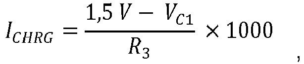
- Batterieladegerät gemäß Anspruch 4, wobei der Ladestrom als Folgendes ausgedrückt ist:
- Batterieladegerät gemäß einem der vorhergehenden Ansprüche, das ferner eine Widerstands(R5)- und Kondensator(C2)-Komponentenschaltung beinhaltet, wobei die Widerstands(R5)- und Kondensator(C2)-Komponentenschaltung als ein Tiefpassfilter betriebsfähig ist, um das Referenzspannungssignal (VP) zu filtern.
- Batterieladegerät gemäß einem der vorhergehenden Ansprüche, wobei der Widerstand (R5) der Widerstands- und Kondensatorkomponentenschaltung betriebsfähig ist, um andere Komponenten von der Batterieladungssteuereinheit (52) zu isolieren.
- Batterieladegerät gemäß einem der vorhergehenden Ansprüche, wobei die Batterieladungssteuereinheit (52) in einem Konstantstrommodus betriebsfähig ist.
- Batterieladegerät gemäß einem der vorhergehenden Ansprüche, wobei der Vergleichsmesser ein Vergleichsmesser mit offenem Drain ist und betriebsfähig ist, um Strom in den Ausgang des Vergleichsmessers (50) zu versenken, wenn das Spannungssignal (VN) größer als das Referenzspannungssignal (VP) ist.
- Batterieladegerät gemäß einem der vorhergehenden Ansprüche, wobei das Spannungssignal (VN) mit dem invertierenden Eingang des Vergleichsmessers (50) gekoppelt ist und das Referenzspannungssignal (VP) mit dem nichtinvertierenden Eingang des Vergleichsmessers (50) gekoppelt ist.
- Batterieladegerät gemäß Anspruch 3, wobei, wenn:

wobei VHSY eine Eingangshysterese des Vergleichsmessers (52) ist. - Batterieladegerät gemäß Anspruch 3 oder 11, wobei, wenn:

wobei VHSY eine Eingangshysterese des Vergleichsmessers (52) ist.
Applications Claiming Priority (5)
| Application Number | Priority Date | Filing Date | Title |
|---|---|---|---|
| CA002419497A CA2419497C (en) | 2003-02-21 | 2003-02-21 | Circuit and method of operation for an adaptive charge rate power supply |
| US10/372,446 US6833686B2 (en) | 2003-02-21 | 2003-02-21 | Circuit and method of operation for an adaptive charge rate power supply |
| PCT/CA2004/000248 WO2004075039A1 (en) | 2003-02-21 | 2004-02-20 | Circuit and method of operation for an adaptive charge rate power supply |
| EP04712981A EP1595203B8 (de) | 2003-02-21 | 2004-02-20 | Schaltung und verfahren zum betrieb für ein netzteil mit adaptiver ladegeschwindigkeit |
| EP10181666.8A EP2264855B1 (de) | 2003-02-21 | 2004-02-20 | Schaltung und Betriebsverfahren für ein Netzteil mit adaptativer Ladegeschwindigkeit |
Related Parent Applications (3)
| Application Number | Title | Priority Date | Filing Date |
|---|---|---|---|
| EP10181666.8A Division EP2264855B1 (de) | 2003-02-21 | 2004-02-20 | Schaltung und Betriebsverfahren für ein Netzteil mit adaptativer Ladegeschwindigkeit |
| EP10181666.8A Division-Into EP2264855B1 (de) | 2003-02-21 | 2004-02-20 | Schaltung und Betriebsverfahren für ein Netzteil mit adaptativer Ladegeschwindigkeit |
| EP04712981A Division EP1595203B8 (de) | 2003-02-21 | 2004-02-20 | Schaltung und verfahren zum betrieb für ein netzteil mit adaptiver ladegeschwindigkeit |
Publications (2)
| Publication Number | Publication Date |
|---|---|
| EP3674844A1 EP3674844A1 (de) | 2020-07-01 |
| EP3674844B1 true EP3674844B1 (de) | 2022-07-06 |
Family
ID=32909237
Family Applications (3)
| Application Number | Title | Priority Date | Filing Date |
|---|---|---|---|
| EP20158210.3A Expired - Lifetime EP3674844B1 (de) | 2003-02-21 | 2004-02-20 | Schaltung und betriebsverfahren für eine adaptive ladungsratenenergieversorgung |
| EP04712981A Expired - Lifetime EP1595203B8 (de) | 2003-02-21 | 2004-02-20 | Schaltung und verfahren zum betrieb für ein netzteil mit adaptiver ladegeschwindigkeit |
| EP10181666.8A Expired - Lifetime EP2264855B1 (de) | 2003-02-21 | 2004-02-20 | Schaltung und Betriebsverfahren für ein Netzteil mit adaptativer Ladegeschwindigkeit |
Family Applications After (2)
| Application Number | Title | Priority Date | Filing Date |
|---|---|---|---|
| EP04712981A Expired - Lifetime EP1595203B8 (de) | 2003-02-21 | 2004-02-20 | Schaltung und verfahren zum betrieb für ein netzteil mit adaptiver ladegeschwindigkeit |
| EP10181666.8A Expired - Lifetime EP2264855B1 (de) | 2003-02-21 | 2004-02-20 | Schaltung und Betriebsverfahren für ein Netzteil mit adaptativer Ladegeschwindigkeit |
Country Status (4)
| Country | Link |
|---|---|
| EP (3) | EP3674844B1 (de) |
| AT (1) | ATE496327T1 (de) |
| DE (1) | DE602004031082D1 (de) |
| WO (1) | WO2004075039A1 (de) |
Families Citing this family (7)
| Publication number | Priority date | Publication date | Assignee | Title |
|---|---|---|---|---|
| US20060023410A1 (en) * | 2004-07-30 | 2006-02-02 | Mark Solomon | Apparatus for storing a structure within an electronic device |
| AT502552B1 (de) * | 2005-10-11 | 2007-07-15 | Fronius Int Gmbh | Montagemethode, kupplungsvorrichtung und kupplungselement für einen hochleistungskontakt, sowie batterieladegerät mit einer kupplungsvorrichtung |
| US8350522B2 (en) | 2010-03-10 | 2013-01-08 | Apple Inc. | External power source voltage drop compensation for portable devices |
| GB201300301D0 (en) * | 2013-01-08 | 2013-02-20 | Levy Joshua | Single USB 2.0 device using GSM voice and mobile internet technology using M2M module, which operates as a full system using hardware and software |
| JP6377836B2 (ja) * | 2014-07-16 | 2018-08-22 | 華為技術有限公司Huawei Technologies Co.,Ltd. | 電子デバイス高速充電方法、装置、及びデバイス |
| CN108919871A (zh) * | 2017-03-30 | 2018-11-30 | 立锜科技股份有限公司 | 电源传输装置 |
| US10741348B2 (en) * | 2017-03-30 | 2020-08-11 | Richtek Technology Corporation | Power transmission apparatus |
Family Cites Families (5)
| Publication number | Priority date | Publication date | Assignee | Title |
|---|---|---|---|---|
| US5723970A (en) * | 1996-04-05 | 1998-03-03 | Linear Technology Corporation | Battery charging circuitry having supply current regulation |
| US6300744B1 (en) * | 2000-02-10 | 2001-10-09 | Siliconix Incorporated | High-efficiency battery charger |
| US6507172B2 (en) * | 2001-03-19 | 2003-01-14 | Maxim Integrated Products, Inc. | Universal serial bus powered battery charger |
| US6522118B1 (en) * | 2001-04-18 | 2003-02-18 | Linear Technology Corporation | Constant-current/constant-voltage current supply |
| US6507173B1 (en) * | 2001-06-22 | 2003-01-14 | 02 Micro International Limited | Single chip power management unit apparatus and method |
-
2004
- 2004-02-20 EP EP20158210.3A patent/EP3674844B1/de not_active Expired - Lifetime
- 2004-02-20 WO PCT/CA2004/000248 patent/WO2004075039A1/en not_active Ceased
- 2004-02-20 EP EP04712981A patent/EP1595203B8/de not_active Expired - Lifetime
- 2004-02-20 EP EP10181666.8A patent/EP2264855B1/de not_active Expired - Lifetime
- 2004-02-20 DE DE602004031082T patent/DE602004031082D1/de not_active Expired - Lifetime
- 2004-02-20 AT AT04712981T patent/ATE496327T1/de not_active IP Right Cessation
Also Published As
| Publication number | Publication date |
|---|---|
| EP3674844A1 (de) | 2020-07-01 |
| DE602004031082D1 (de) | 2011-03-03 |
| ATE496327T1 (de) | 2011-02-15 |
| EP1595203A1 (de) | 2005-11-16 |
| EP1595203B1 (de) | 2011-01-19 |
| WO2004075039A1 (en) | 2004-09-02 |
| EP2264855B1 (de) | 2020-04-08 |
| WO2004075039A8 (en) | 2012-04-12 |
| EP2264855A3 (de) | 2012-04-04 |
| EP2264855A2 (de) | 2010-12-22 |
| EP1595203B8 (de) | 2012-04-18 |
| HK1082572A1 (en) | 2006-06-09 |
Similar Documents
| Publication | Publication Date | Title |
|---|---|---|
| US6833686B2 (en) | Circuit and method of operation for an adaptive charge rate power supply | |
| JP4197189B2 (ja) | 電力供給のための回路および動作方法 | |
| US8541983B2 (en) | Circuit and method of operation for an electrical power supply | |
| US9231435B2 (en) | Methods and apparatuses for operating devices with solar power | |
| US20080084177A1 (en) | Portable devices having multiple power interfaces | |
| KR20090114335A (ko) | 충전 배터리 전류의 부하 전류 의존도 감소 | |
| EP3674844B1 (de) | Schaltung und betriebsverfahren für eine adaptive ladungsratenenergieversorgung | |
| CA2419497C (en) | Circuit and method of operation for an adaptive charge rate power supply | |
| HK1082572B (en) | Circuit and method of operation for an adaptive charge rate power supply | |
| CA2419488C (en) | Circuit and method of operation for an electrical power supply | |
| US6967467B2 (en) | Method and apparatus for current delegation to a plurality of loads | |
| HK1082600B (en) | Circuit and method of operation for an electrical power supply | |
| HK1082600A (en) | Circuit and method of operation for an electrical power supply |
Legal Events
| Date | Code | Title | Description |
|---|---|---|---|
| PUAI | Public reference made under article 153(3) epc to a published international application that has entered the european phase |
Free format text: ORIGINAL CODE: 0009012 |
|
| STAA | Information on the status of an ep patent application or granted ep patent |
Free format text: STATUS: THE APPLICATION HAS BEEN PUBLISHED |
|
| AC | Divisional application: reference to earlier application |
Ref document number: 2264855 Country of ref document: EP Kind code of ref document: P Ref document number: 1595203 Country of ref document: EP Kind code of ref document: P |
|
| AK | Designated contracting states |
Kind code of ref document: A1 Designated state(s): AT BE BG CH CY CZ DE DK EE ES FI FR GB GR HU IE IT LI LU MC NL PT RO SE SI SK TR |
|
| STAA | Information on the status of an ep patent application or granted ep patent |
Free format text: STATUS: REQUEST FOR EXAMINATION WAS MADE |
|
| 17P | Request for examination filed |
Effective date: 20201211 |
|
| RBV | Designated contracting states (corrected) |
Designated state(s): AT BE BG CH CY CZ DE DK EE ES FI FR GB GR HU IE IT LI LU MC NL PT RO SE SI SK TR |
|
| GRAP | Despatch of communication of intention to grant a patent |
Free format text: ORIGINAL CODE: EPIDOSNIGR1 |
|
| STAA | Information on the status of an ep patent application or granted ep patent |
Free format text: STATUS: GRANT OF PATENT IS INTENDED |
|
| INTG | Intention to grant announced |
Effective date: 20220203 |
|
| GRAS | Grant fee paid |
Free format text: ORIGINAL CODE: EPIDOSNIGR3 |
|
| GRAA | (expected) grant |
Free format text: ORIGINAL CODE: 0009210 |
|
| STAA | Information on the status of an ep patent application or granted ep patent |
Free format text: STATUS: THE PATENT HAS BEEN GRANTED |
|
| AC | Divisional application: reference to earlier application |
Ref document number: 1595203 Country of ref document: EP Kind code of ref document: P Ref document number: 2264855 Country of ref document: EP Kind code of ref document: P |
|
| AK | Designated contracting states |
Kind code of ref document: B1 Designated state(s): AT BE BG CH CY CZ DE DK EE ES FI FR GB GR HU IE IT LI LU MC NL PT RO SE SI SK TR |
|
| REG | Reference to a national code |
Ref country code: AT Ref legal event code: REF Ref document number: 1503317 Country of ref document: AT Kind code of ref document: T Effective date: 20220715 Ref country code: CH Ref legal event code: EP |
|
| REG | Reference to a national code |
Ref country code: DE Ref legal event code: R096 Ref document number: 602004055093 Country of ref document: DE |
|
| REG | Reference to a national code |
Ref country code: IE Ref legal event code: FG4D |
|
| REG | Reference to a national code |
Ref country code: NL Ref legal event code: MP Effective date: 20220706 |
|
| PG25 | Lapsed in a contracting state [announced via postgrant information from national office to epo] |
Ref country code: SE Free format text: LAPSE BECAUSE OF FAILURE TO SUBMIT A TRANSLATION OF THE DESCRIPTION OR TO PAY THE FEE WITHIN THE PRESCRIBED TIME-LIMIT Effective date: 20220706 Ref country code: PT Free format text: LAPSE BECAUSE OF FAILURE TO SUBMIT A TRANSLATION OF THE DESCRIPTION OR TO PAY THE FEE WITHIN THE PRESCRIBED TIME-LIMIT Effective date: 20221107 Ref country code: NL Free format text: LAPSE BECAUSE OF FAILURE TO SUBMIT A TRANSLATION OF THE DESCRIPTION OR TO PAY THE FEE WITHIN THE PRESCRIBED TIME-LIMIT Effective date: 20220706 Ref country code: FI Free format text: LAPSE BECAUSE OF FAILURE TO SUBMIT A TRANSLATION OF THE DESCRIPTION OR TO PAY THE FEE WITHIN THE PRESCRIBED TIME-LIMIT Effective date: 20220706 Ref country code: ES Free format text: LAPSE BECAUSE OF FAILURE TO SUBMIT A TRANSLATION OF THE DESCRIPTION OR TO PAY THE FEE WITHIN THE PRESCRIBED TIME-LIMIT Effective date: 20220706 |
|
| REG | Reference to a national code |
Ref country code: AT Ref legal event code: MK05 Ref document number: 1503317 Country of ref document: AT Kind code of ref document: T Effective date: 20220706 |
|
| PG25 | Lapsed in a contracting state [announced via postgrant information from national office to epo] |
Ref country code: GR Free format text: LAPSE BECAUSE OF FAILURE TO SUBMIT A TRANSLATION OF THE DESCRIPTION OR TO PAY THE FEE WITHIN THE PRESCRIBED TIME-LIMIT Effective date: 20221007 |
|
| REG | Reference to a national code |
Ref country code: DE Ref legal event code: R097 Ref document number: 602004055093 Country of ref document: DE |
|
| PG25 | Lapsed in a contracting state [announced via postgrant information from national office to epo] |
Ref country code: RO Free format text: LAPSE BECAUSE OF FAILURE TO SUBMIT A TRANSLATION OF THE DESCRIPTION OR TO PAY THE FEE WITHIN THE PRESCRIBED TIME-LIMIT Effective date: 20220706 Ref country code: DK Free format text: LAPSE BECAUSE OF FAILURE TO SUBMIT A TRANSLATION OF THE DESCRIPTION OR TO PAY THE FEE WITHIN THE PRESCRIBED TIME-LIMIT Effective date: 20220706 Ref country code: CZ Free format text: LAPSE BECAUSE OF FAILURE TO SUBMIT A TRANSLATION OF THE DESCRIPTION OR TO PAY THE FEE WITHIN THE PRESCRIBED TIME-LIMIT Effective date: 20220706 Ref country code: AT Free format text: LAPSE BECAUSE OF FAILURE TO SUBMIT A TRANSLATION OF THE DESCRIPTION OR TO PAY THE FEE WITHIN THE PRESCRIBED TIME-LIMIT Effective date: 20220706 |
|
| PGFP | Annual fee paid to national office [announced via postgrant information from national office to epo] |
Ref country code: FR Payment date: 20230223 Year of fee payment: 20 |
|
| PLBE | No opposition filed within time limit |
Free format text: ORIGINAL CODE: 0009261 |
|
| STAA | Information on the status of an ep patent application or granted ep patent |
Free format text: STATUS: NO OPPOSITION FILED WITHIN TIME LIMIT |
|
| PG25 | Lapsed in a contracting state [announced via postgrant information from national office to epo] |
Ref country code: SK Free format text: LAPSE BECAUSE OF FAILURE TO SUBMIT A TRANSLATION OF THE DESCRIPTION OR TO PAY THE FEE WITHIN THE PRESCRIBED TIME-LIMIT Effective date: 20220706 Ref country code: EE Free format text: LAPSE BECAUSE OF FAILURE TO SUBMIT A TRANSLATION OF THE DESCRIPTION OR TO PAY THE FEE WITHIN THE PRESCRIBED TIME-LIMIT Effective date: 20220706 |
|
| PGFP | Annual fee paid to national office [announced via postgrant information from national office to epo] |
Ref country code: GB Payment date: 20230227 Year of fee payment: 20 Ref country code: DE Payment date: 20230223 Year of fee payment: 20 |
|
| 26N | No opposition filed |
Effective date: 20230411 |
|
| PG25 | Lapsed in a contracting state [announced via postgrant information from national office to epo] |
Ref country code: SI Free format text: LAPSE BECAUSE OF FAILURE TO SUBMIT A TRANSLATION OF THE DESCRIPTION OR TO PAY THE FEE WITHIN THE PRESCRIBED TIME-LIMIT Effective date: 20220706 |
|
| PG25 | Lapsed in a contracting state [announced via postgrant information from national office to epo] |
Ref country code: MC Free format text: LAPSE BECAUSE OF FAILURE TO SUBMIT A TRANSLATION OF THE DESCRIPTION OR TO PAY THE FEE WITHIN THE PRESCRIBED TIME-LIMIT Effective date: 20220706 |
|
| REG | Reference to a national code |
Ref country code: CH Ref legal event code: PL |
|
| REG | Reference to a national code |
Ref country code: BE Ref legal event code: MM Effective date: 20230228 |
|
| PG25 | Lapsed in a contracting state [announced via postgrant information from national office to epo] |
Ref country code: LU Free format text: LAPSE BECAUSE OF NON-PAYMENT OF DUE FEES Effective date: 20230220 Ref country code: LI Free format text: LAPSE BECAUSE OF NON-PAYMENT OF DUE FEES Effective date: 20230228 Ref country code: CH Free format text: LAPSE BECAUSE OF NON-PAYMENT OF DUE FEES Effective date: 20230228 |
|
| REG | Reference to a national code |
Ref country code: IE Ref legal event code: MM4A |
|
| PG25 | Lapsed in a contracting state [announced via postgrant information from national office to epo] |
Ref country code: IT Free format text: LAPSE BECAUSE OF FAILURE TO SUBMIT A TRANSLATION OF THE DESCRIPTION OR TO PAY THE FEE WITHIN THE PRESCRIBED TIME-LIMIT Effective date: 20220706 Ref country code: IE Free format text: LAPSE BECAUSE OF NON-PAYMENT OF DUE FEES Effective date: 20230220 |
|
| REG | Reference to a national code |
Ref country code: DE Ref legal event code: R071 Ref document number: 602004055093 Country of ref document: DE |
|
| PG25 | Lapsed in a contracting state [announced via postgrant information from national office to epo] |
Ref country code: BE Free format text: LAPSE BECAUSE OF NON-PAYMENT OF DUE FEES Effective date: 20230228 |
|
| REG | Reference to a national code |
Ref country code: GB Ref legal event code: PE20 Expiry date: 20240219 |
|
| PG25 | Lapsed in a contracting state [announced via postgrant information from national office to epo] |
Ref country code: GB Free format text: LAPSE BECAUSE OF EXPIRATION OF PROTECTION Effective date: 20240219 |
|
| REG | Reference to a national code |
Ref country code: DE Ref legal event code: R082 Ref document number: 602004055093 Country of ref document: DE Ref country code: DE Ref legal event code: R081 Ref document number: 602004055093 Country of ref document: DE Owner name: MALIKIE INNOVATIONS LTD., IE Free format text: FORMER OWNER: BLACKBERRY LIMITED, WATERLOO, ON, CA |
|
| REG | Reference to a national code |
Ref country code: GB Ref legal event code: 732E Free format text: REGISTERED BETWEEN 20240530 AND 20240605 |
|
| PG25 | Lapsed in a contracting state [announced via postgrant information from national office to epo] |
Ref country code: BG Free format text: LAPSE BECAUSE OF FAILURE TO SUBMIT A TRANSLATION OF THE DESCRIPTION OR TO PAY THE FEE WITHIN THE PRESCRIBED TIME-LIMIT Effective date: 20220706 |
|
| PG25 | Lapsed in a contracting state [announced via postgrant information from national office to epo] |
Ref country code: BG Free format text: LAPSE BECAUSE OF FAILURE TO SUBMIT A TRANSLATION OF THE DESCRIPTION OR TO PAY THE FEE WITHIN THE PRESCRIBED TIME-LIMIT Effective date: 20220706 |
|
| PG25 | Lapsed in a contracting state [announced via postgrant information from national office to epo] |
Ref country code: CY Free format text: LAPSE BECAUSE OF FAILURE TO SUBMIT A TRANSLATION OF THE DESCRIPTION OR TO PAY THE FEE WITHIN THE PRESCRIBED TIME-LIMIT; INVALID AB INITIO Effective date: 20040220 |
|
| PG25 | Lapsed in a contracting state [announced via postgrant information from national office to epo] |
Ref country code: HU Free format text: LAPSE BECAUSE OF FAILURE TO SUBMIT A TRANSLATION OF THE DESCRIPTION OR TO PAY THE FEE WITHIN THE PRESCRIBED TIME-LIMIT; INVALID AB INITIO Effective date: 20040220 |
|
| PG25 | Lapsed in a contracting state [announced via postgrant information from national office to epo] |
Ref country code: TR Free format text: LAPSE BECAUSE OF FAILURE TO SUBMIT A TRANSLATION OF THE DESCRIPTION OR TO PAY THE FEE WITHIN THE PRESCRIBED TIME-LIMIT Effective date: 20220706 |