EP3674700A1 - Sensorsubstrat und damit versehene sensorvorrichtung - Google Patents
Sensorsubstrat und damit versehene sensorvorrichtung Download PDFInfo
- Publication number
- EP3674700A1 EP3674700A1 EP18847958.8A EP18847958A EP3674700A1 EP 3674700 A1 EP3674700 A1 EP 3674700A1 EP 18847958 A EP18847958 A EP 18847958A EP 3674700 A1 EP3674700 A1 EP 3674700A1
- Authority
- EP
- European Patent Office
- Prior art keywords
- electrode
- negative electrode
- positive electrode
- insulating substrate
- positive
- Prior art date
- Legal status (The legal status is an assumption and is not a legal conclusion. Google has not performed a legal analysis and makes no representation as to the accuracy of the status listed.)
- Withdrawn
Links
- 239000000758 substrate Substances 0.000 title claims abstract description 63
- 238000001514 detection method Methods 0.000 claims abstract description 67
- 230000002093 peripheral effect Effects 0.000 claims description 22
- 239000004020 conductor Substances 0.000 claims description 19
- 239000013618 particulate matter Substances 0.000 description 23
- 239000004071 soot Substances 0.000 description 20
- 239000000463 material Substances 0.000 description 14
- 239000000919 ceramic Substances 0.000 description 12
- 239000007769 metal material Substances 0.000 description 11
- 229910052751 metal Inorganic materials 0.000 description 8
- 239000002184 metal Substances 0.000 description 8
- XEEYBQQBJWHFJM-UHFFFAOYSA-N Iron Chemical compound [Fe] XEEYBQQBJWHFJM-UHFFFAOYSA-N 0.000 description 6
- BASFCYQUMIYNBI-UHFFFAOYSA-N platinum Chemical compound [Pt] BASFCYQUMIYNBI-UHFFFAOYSA-N 0.000 description 6
- 239000010953 base metal Substances 0.000 description 5
- 238000005219 brazing Methods 0.000 description 5
- 230000006866 deterioration Effects 0.000 description 5
- TWNQGVIAIRXVLR-UHFFFAOYSA-N oxo(oxoalumanyloxy)alumane Chemical compound O=[Al]O[Al]=O TWNQGVIAIRXVLR-UHFFFAOYSA-N 0.000 description 5
- 230000007547 defect Effects 0.000 description 4
- 238000009791 electrochemical migration reaction Methods 0.000 description 4
- 238000010438 heat treatment Methods 0.000 description 4
- AMWRITDGCCNYAT-UHFFFAOYSA-L hydroxy(oxo)manganese;manganese Chemical compound [Mn].O[Mn]=O.O[Mn]=O AMWRITDGCCNYAT-UHFFFAOYSA-L 0.000 description 4
- 238000004519 manufacturing process Methods 0.000 description 4
- 238000002161 passivation Methods 0.000 description 4
- PCHJSUWPFVWCPO-UHFFFAOYSA-N gold Chemical compound [Au] PCHJSUWPFVWCPO-UHFFFAOYSA-N 0.000 description 3
- 229910052737 gold Inorganic materials 0.000 description 3
- 239000010931 gold Substances 0.000 description 3
- 229910052742 iron Inorganic materials 0.000 description 3
- 238000000034 method Methods 0.000 description 3
- 229910052697 platinum Inorganic materials 0.000 description 3
- 239000000843 powder Substances 0.000 description 3
- PXHVJJICTQNCMI-UHFFFAOYSA-N Nickel Chemical compound [Ni] PXHVJJICTQNCMI-UHFFFAOYSA-N 0.000 description 2
- VYPSYNLAJGMNEJ-UHFFFAOYSA-N Silicium dioxide Chemical compound O=[Si]=O VYPSYNLAJGMNEJ-UHFFFAOYSA-N 0.000 description 2
- 229910045601 alloy Inorganic materials 0.000 description 2
- 239000000956 alloy Substances 0.000 description 2
- 239000011230 binding agent Substances 0.000 description 2
- 230000005684 electric field Effects 0.000 description 2
- 238000010292 electrical insulation Methods 0.000 description 2
- CPLXHLVBOLITMK-UHFFFAOYSA-N magnesium oxide Inorganic materials [Mg]=O CPLXHLVBOLITMK-UHFFFAOYSA-N 0.000 description 2
- 239000000395 magnesium oxide Substances 0.000 description 2
- AXZKOIWUVFPNLO-UHFFFAOYSA-N magnesium;oxygen(2-) Chemical compound [O-2].[Mg+2] AXZKOIWUVFPNLO-UHFFFAOYSA-N 0.000 description 2
- 150000002739 metals Chemical class 0.000 description 2
- 239000000203 mixture Substances 0.000 description 2
- 230000003647 oxidation Effects 0.000 description 2
- 238000007254 oxidation reaction Methods 0.000 description 2
- 238000007747 plating Methods 0.000 description 2
- 238000004080 punching Methods 0.000 description 2
- 229910052814 silicon oxide Inorganic materials 0.000 description 2
- 239000002002 slurry Substances 0.000 description 2
- WFKWXMTUELFFGS-UHFFFAOYSA-N tungsten Chemical compound [W] WFKWXMTUELFFGS-UHFFFAOYSA-N 0.000 description 2
- 229910052721 tungsten Inorganic materials 0.000 description 2
- 239000010937 tungsten Substances 0.000 description 2
- OKTJSMMVPCPJKN-UHFFFAOYSA-N Carbon Chemical compound [C] OKTJSMMVPCPJKN-UHFFFAOYSA-N 0.000 description 1
- VYZAMTAEIAYCRO-UHFFFAOYSA-N Chromium Chemical compound [Cr] VYZAMTAEIAYCRO-UHFFFAOYSA-N 0.000 description 1
- 229910000531 Co alloy Inorganic materials 0.000 description 1
- RYGMFSIKBFXOCR-UHFFFAOYSA-N Copper Chemical compound [Cu] RYGMFSIKBFXOCR-UHFFFAOYSA-N 0.000 description 1
- ZOKXTWBITQBERF-UHFFFAOYSA-N Molybdenum Chemical compound [Mo] ZOKXTWBITQBERF-UHFFFAOYSA-N 0.000 description 1
- XUIMIQQOPSSXEZ-UHFFFAOYSA-N Silicon Chemical compound [Si] XUIMIQQOPSSXEZ-UHFFFAOYSA-N 0.000 description 1
- BQCADISMDOOEFD-UHFFFAOYSA-N Silver Chemical compound [Ag] BQCADISMDOOEFD-UHFFFAOYSA-N 0.000 description 1
- RTAQQCXQSZGOHL-UHFFFAOYSA-N Titanium Chemical compound [Ti] RTAQQCXQSZGOHL-UHFFFAOYSA-N 0.000 description 1
- QCWXUUIWCKQGHC-UHFFFAOYSA-N Zirconium Chemical compound [Zr] QCWXUUIWCKQGHC-UHFFFAOYSA-N 0.000 description 1
- NEIHULKJZQTQKJ-UHFFFAOYSA-N [Cu].[Ag] Chemical compound [Cu].[Ag] NEIHULKJZQTQKJ-UHFFFAOYSA-N 0.000 description 1
- KGWWEXORQXHJJQ-UHFFFAOYSA-N [Fe].[Co].[Ni] Chemical compound [Fe].[Co].[Ni] KGWWEXORQXHJJQ-UHFFFAOYSA-N 0.000 description 1
- 230000005856 abnormality Effects 0.000 description 1
- 229910052782 aluminium Inorganic materials 0.000 description 1
- XAGFODPZIPBFFR-UHFFFAOYSA-N aluminium Chemical compound [Al] XAGFODPZIPBFFR-UHFFFAOYSA-N 0.000 description 1
- 238000003490 calendering Methods 0.000 description 1
- 229910052804 chromium Inorganic materials 0.000 description 1
- 239000011651 chromium Substances 0.000 description 1
- 230000000052 comparative effect Effects 0.000 description 1
- 229910052802 copper Inorganic materials 0.000 description 1
- 239000010949 copper Substances 0.000 description 1
- PMHQVHHXPFUNSP-UHFFFAOYSA-M copper(1+);methylsulfanylmethane;bromide Chemical compound Br[Cu].CSC PMHQVHHXPFUNSP-UHFFFAOYSA-M 0.000 description 1
- 238000000354 decomposition reaction Methods 0.000 description 1
- 230000008021 deposition Effects 0.000 description 1
- KZHJGOXRZJKJNY-UHFFFAOYSA-N dioxosilane;oxo(oxoalumanyloxy)alumane Chemical compound O=[Si]=O.O=[Si]=O.O=[Al]O[Al]=O.O=[Al]O[Al]=O.O=[Al]O[Al]=O KZHJGOXRZJKJNY-UHFFFAOYSA-N 0.000 description 1
- 230000005611 electricity Effects 0.000 description 1
- 238000011049 filling Methods 0.000 description 1
- 238000010304 firing Methods 0.000 description 1
- 239000002241 glass-ceramic Substances 0.000 description 1
- 238000009434 installation Methods 0.000 description 1
- 238000003754 machining Methods 0.000 description 1
- 229910021645 metal ion Inorganic materials 0.000 description 1
- 230000005012 migration Effects 0.000 description 1
- 238000013508 migration Methods 0.000 description 1
- 229910052750 molybdenum Inorganic materials 0.000 description 1
- 239000011733 molybdenum Substances 0.000 description 1
- 229910052863 mullite Inorganic materials 0.000 description 1
- 229910052759 nickel Inorganic materials 0.000 description 1
- 239000003960 organic solvent Substances 0.000 description 1
- RVTZCBVAJQQJTK-UHFFFAOYSA-N oxygen(2-);zirconium(4+) Chemical compound [O-2].[O-2].[Zr+4] RVTZCBVAJQQJTK-UHFFFAOYSA-N 0.000 description 1
- 239000004014 plasticizer Substances 0.000 description 1
- 239000002994 raw material Substances 0.000 description 1
- 230000008929 regeneration Effects 0.000 description 1
- 238000011069 regeneration method Methods 0.000 description 1
- 238000007650 screen-printing Methods 0.000 description 1
- 230000035945 sensitivity Effects 0.000 description 1
- 229910052710 silicon Inorganic materials 0.000 description 1
- 239000010703 silicon Substances 0.000 description 1
- 229910052709 silver Inorganic materials 0.000 description 1
- 239000004332 silver Substances 0.000 description 1
- 238000005245 sintering Methods 0.000 description 1
- 239000002904 solvent Substances 0.000 description 1
- 229910052719 titanium Inorganic materials 0.000 description 1
- 239000010936 titanium Substances 0.000 description 1
- 229910052726 zirconium Inorganic materials 0.000 description 1
- 229910001928 zirconium oxide Inorganic materials 0.000 description 1
Images


Classifications
-
- G—PHYSICS
- G01—MEASURING; TESTING
- G01N—INVESTIGATING OR ANALYSING MATERIALS BY DETERMINING THEIR CHEMICAL OR PHYSICAL PROPERTIES
- G01N15/00—Investigating characteristics of particles; Investigating permeability, pore-volume or surface-area of porous materials
- G01N15/06—Investigating concentration of particle suspensions
- G01N15/0656—Investigating concentration of particle suspensions using electric, e.g. electrostatic methods or magnetic methods
-
- G—PHYSICS
- G01—MEASURING; TESTING
- G01N—INVESTIGATING OR ANALYSING MATERIALS BY DETERMINING THEIR CHEMICAL OR PHYSICAL PROPERTIES
- G01N15/00—Investigating characteristics of particles; Investigating permeability, pore-volume or surface-area of porous materials
- G01N15/06—Investigating concentration of particle suspensions
- G01N15/0606—Investigating concentration of particle suspensions by collecting particles on a support
-
- G—PHYSICS
- G01—MEASURING; TESTING
- G01N—INVESTIGATING OR ANALYSING MATERIALS BY DETERMINING THEIR CHEMICAL OR PHYSICAL PROPERTIES
- G01N27/00—Investigating or analysing materials by the use of electric, electrochemical, or magnetic means
- G01N27/02—Investigating or analysing materials by the use of electric, electrochemical, or magnetic means by investigating impedance
- G01N27/04—Investigating or analysing materials by the use of electric, electrochemical, or magnetic means by investigating impedance by investigating resistance
Definitions
- the present invention relates to a sensor board and a sensor device including the sensor board.
- Automobiles may incorporate a diesel particulate filter (DPF) to collect particulate matter (PM) mainly containing soot in exhaust gas.
- DPF diesel particulate filter
- a known PM detector that serves as a PM detection sensor may include an insulating substrate formed from sintered ceramics, such as sintered aluminum oxide, and detection electrodes located on the surface of the insulating substrate. The detector detects particulate matter based on a change in the electrical characteristics caused by a detection target, such as PM contained in exhaust gas, adhering between a pair of detection electrodes (refer to, for example, Japanese Unexamined Patent Application Publication Nos. 2012-47596 and 2014-32063 ).
- the PM detection sensor may include more pairs of detection electrodes. However, more pairs of detection electrodes use a larger area on the insulating substrate.
- the PM detection sensor including a larger insulating substrate cannot be downsized.
- a sensor board includes an insulating substrate, detection electrode located on a surface of the insulating substrate and including a positive electrode and a negative electrode adjacent to each other, and connection terminal including a positive electrode terminal electrically connected to the positive electrode and a negative electrode terminal electrically connected to the negative electrode.
- the negative electrode has a smaller volume than the positive electrode 2.
- a sensor device includes the sensor board with the above structure, and a direct current power source connected to the connection terminals.
- Fig. 1A is a top view of a sensor board according to a first embodiment of the present invention
- Fig. 1B is a cross-sectional view taken along line A-A in Fig. 1A .
- a sensor board 10 is included in a sensor device for detecting particulate matter (PM) such as soot in exhaust gas from, for example, a diesel engine vehicle or a gasoline engine vehicle (e.g., installed on a path for exhaust gas from an automobile).
- the sensor board 10 includes an insulating substrate 1 having an upper surface and a lower surface, detection electrode K including a positive electrode 2 and a negative electrode 3 located on at least one surface of the insulating substrate 1, and connection terminal T located on at least one surface of the insulating substrate 1 and including a positive electrode terminal 4 electrically connected to the positive electrode 2 and a negative electrode terminal 5 electrically connected to the negative electrode 3.
- the sensor board 10 includes heat generators 6 inside the insulating substrate 1 and the detection electrode K is located on both the upper and lower surfaces of the insulating substrate 1.
- the insulating substrate 1 which may be a rectangular plate (thin rectangular prism), serves as a base to receive the positive electrode 2 and the negative electrode 3 included in the detection electrode K in an electrically insulated manner.
- the insulating substrate 1 is formed from sintered ceramics, such as sintered aluminum oxide, sintered aluminum nitride, sintered mullite, sintered glass ceramic, or zirconium ceramic (sintered zirconium oxide).
- the insulating substrate 1 is a stack of multiple insulating layers formed from such sintered ceramics.
- the insulating substrate 1 may be fabricated by, for example, stacking multiple insulating layers formed from sintered aluminum oxide in the manner described below.
- the insulating substrate 1 fabricated in the manner described below includes the vertically stacked insulating layers sintered with one another at their interfaces with no clearly viewable boundary between these insulating layers.
- a raw material powder such as silicon oxide (SiO 2 ), magnesium oxide (MgO), or manganese oxide (Mn 2 O 3 ) is first added to an aluminum oxide (Al 2 O 3 ) powder as a sintering aid, and an appropriate binder, solvent, and plasticizer are further added to the mixture.
- the mixture is then kneaded to prepare ceramic slurry.
- the ceramic slurry is then shaped into a sheet using a method such as a doctor blade or by calendering to obtain a ceramic green sheet.
- the ceramic green sheet then undergoes punching as appropriate.
- Multiple ceramic green sheets prepared in this manner are stacked on one another as appropriate and fired at high temperatures (about 1300 to 1600 °C). The above processes allow the fabrication of the insulating substrate 1.
- the detection electrode K includes the positive electrode 2 and the negative electrode 3 located adjacent to each other.
- the detection electrode K including the positive electrode 2 and the negative electrode 3 may be simply referred to as electrodes without being distinguished from each other.
- the detection electrode K located on the upper surface of the insulating substrate 1 and those located on the lower surface of the insulating substrate 1 may be collectively referred to as the detection electrode K without being distinguished from each other.
- the positive electrode 2 and the negative electrode 3 may have lower electrical insulation or be short-circuited due to particulate matter such as soot adhering to the insulating substrate 1. This allows detection of soot or other matter in the installation environment of the sensor board 10.
- An electrical short circuit between the positive electrode 2 and the negative electrode 3 can be detected by, for example, an external detection circuit connected to the electrodes.
- the environment contains, for example, the exhaust gas from an automobile described above.
- connection terminal T is located on at least one surface of the insulating substrate 1 (upper and lower surfaces in the example shown in Figs. 1A and 1B ).
- the connection terminal T is electrically connected to the positive electrode 2 or the negative electrode 3 and apply a positive or negative potential to the electrodes.
- the sensor board 10 according to the present embodiment includes a positive electrode terminal 4 electrically connected to the positive electrode 2, and a negative electrode terminal 5 electrically connected to the negative electrode 3.
- the positive electrode terminal 4 and the negative electrode terminal 5 form the connection terminal T described above.
- the detection electrode K including the positive electrode 2 and the negative electrode 3 as well as the connection terminal T including the positive electrode terminal 4 and the negative electrode terminal 5 are formed from a metal material that does not oxidize entirely in an environment containing, for example, a high-temperature air current (at about, for example, several hundreds to 1000 °C), such as exhaust gas from an automobile. This allows detection of particulate matter for a longer period of time.
- metal materials include easily-passivatable metals and platinum. Electrodes made of platinum are highly resistant to oxidation at high temperatures, and are thus unlikely to oxidize entirely. Electrodes made of an easily-passivatable metal have their outer surfaces covered with passivation layers, and are thus unlikely to oxidize entirely.
- Examples of easily-passivatable metals include base metal materials that contain at least one element selected from the group consisting of iron, aluminum, nickel, titanium, chromium, and silicon.
- the metal material for the detection electrode contains, for example, at least one of such base metal materials by at least about 80% by mass.
- the base metal materials do not catalyze decomposition of particulate matter. The use of such materials lowers the likelihood that the adhering particulate matter is decomposed unintentionally and thus increases the detection accuracy.
- the detection electrode K may contain other metal materials different from the base metal materials described above. Such other metal materials may be metal materials that do not easily form passivation layers, and may be, for example, tungsten.
- the detection electrode K and the connection terminal T may be formed in the manner described below.
- a powder of at least one of the above base metal materials is kneaded with an organic solvent and a binder to prepare a metal paste.
- the metal paste is then applied, in a predetermined pattern, to a main surface and other areas of a ceramic green sheet to be the insulating substrate 1.
- the metal paste is applied by, for example, screen printing.
- the metal paste and the ceramic green sheet are then co-fired.
- the above processes allow the fabrication of the insulating substrate 1 including the detection electrode K and the connection terminal T on the surface(s).
- connection terminal T may be used in an environment other than a high temperature environment, and may be covered with no passivation layers.
- the connection terminal T may thus be formed from a material selected appropriately in accordance with the situation in which the sensor board 10 is used.
- the connection terminal T may be formed from a metal material such as tungsten or molybdenum.
- the sensor board 10 includes the negative electrode 3 smaller than the positive electrode 2 in a plan view.
- the positive electrode 2 and the negative electrode 3 adjacent to each other each include linear portions (line segments).
- the negative electrode 3 has a smaller (narrower) line width than the positive electrode 2.
- the negative electrode 3 has a smaller volume than the positive electrode 2.
- the size difference between the electrodes is not limited to the difference in a plan view as described above.
- the negative electrode 3 may have the same area as the positive electrode 2 but may be thinner than the positive electrode 2.
- the negative electrode 3 and the positive electrode 2 may have size differences determined with other components.
- the sensor board 10 includes the negative electrode 3 having a relatively small volume (or area or thickness; the same applies hereafter), and can thus be easily downsized.
- the detection electrode K may be arranged more densely to improve the detection accuracy.
- the positive electrode 2 having a relatively large volume (or area or thickness; the same applies hereafter) is less likely to be affected by wear and can reduce electrode function deterioration caused by migration from the positive electrode 2 to the negative electrode 3. More specifically, the electric field between the electrodes may cause electrochemical migration between the electrodes.
- the electrochemical migration induces deposition from the positive electrode to the negative electrode, possibly causing defects such as voids in the positive electrode.
- the positive electrode having a relatively large volume is less likely to be affected by such defects and can reduce electrode function deterioration. This will be described in detail later.
- Particulate matter to be detected includes soot (fine carbon powder), which is easily charged positively. Particulate matter thus tends to adhere to or around the negative electrode 3.
- the negative electrode 3 smaller than (e.g., having a smaller line width than) the positive electrode allows effective detection of, for example, soot adhering to the detection electrodes K.
- the positive electrode 3, which tends to oxidize upon receiving a positive potential, is less susceptible to wear, thus effectively reducing an increase in resistance to electricity passage and breaks in the detection electrode K.
- the sensor board 10 can easily be downsized and have higher detection sensitivity.
- the positive electrode 2 and the negative electrode 3 are interdigitated electrodes. More specifically, the positive electrode 2 and the negative electrode 3 each include multiple linear electrode lines 2a or 3a arranged at intervals in a line width direction and a connection line 2b or 3b linearly interconnecting the ends of the electrode lines 2a or 3a.
- the electrode lines 3a in the negative electrode 3 each have a line width smaller than the line width of an adjacent electrode line 2a included in the positive electrode 2.
- the connection line 2b or 3b may interconnect the ends of the multiple electrode lines 2a or 3a in a different manner, such as in a zigzag manner, rather than linearly as described above.
- the detection electrode K as interdigitated electrodes easily allow the multiple positive and negative electrode lines 2a and 3a to be arranged at small intervals.
- the multiple electrode lines 2a and 3a may easily receive a positive or negative potential collectively.
- the multiple electrode lines 2a in the positive electrode 2 are electrically connected to the positive electrode terminal 4 with the single connection line 2b, which linearly interconnects the ends of the electrode lines 2a.
- the multiple electrode lines 3a in the negative electrode 3 are also electrically connected to the negative electrode terminal 5 with the single connection line 3b, which linearly interconnects the ends of the electrode lines 3a.
- the multiple electrode lines 2a and 3a as the interdigitated electrodes are electrically connected to the connection terminals T (4 and 5) collectively to receive a positive or negative potential.
- the electrode lines 2a in the positive electrode 2 each have a line width of about, for example, 80 to 120 ⁇ m, whereas the electrode lines 3a included in the negative electrode 3 each have a line width of about 40 to 60 ⁇ m. More specifically, the line width of the negative electrode 3 is about 50% the line width of the positive electrode 2.
- the insulating substrate 1 thus has, for example, a plate-like profile with a quadrangular area of about 60 ⁇ 4 mm in a plan view and a thickness of about 600 to 1200 ⁇ m.
- the detection electrode K is located on, for example, a rectangular area with a side length of about 3.0 to 3.6 mm on the upper or lower surface.
- one first electrode pair D1 includes the rightmost negative electrode line 3a and the positive electrode line 2a to the immediate left of the negative electrode line 3a
- one second electrode pair D2 includes the positive electrode line 2a included in the electrode pair D1 and the negative electrode line 3a to the immediate left of the positive electrode line 2a.
- the positive and negative electrode lines 2a and 3a in the middle of the electrode line array are commonly included in the two electrode pairs adjacent to each other.
- a known sensor board including a negative electrode and a positive electrode having the same size includes a fewer electrode line pairs than the sensor board 10 according to the present embodiment. More specifically, when a negative electrode included in a known sensor board has the same line width as the positive electrode in an example sensor board according to the present embodiment with the other components having the same dimensions, the insulating substrate may include about 14 to 29 pairs of electrode lines on each of the upper and lower surfaces. This number is about 83 to 88% of the number of electrode pairs in the sensor board 10 according to the present embodiment.
- the area of the insulating substrate 1 in a plan view can be smaller (about 83 to 89%) in the present embodiment, conversely to the above proportion for the number of pairs.
- the sensor board 10 according to the present embodiment is thus downsized and improves detection accuracy.
- the sensor board 10 includes the heat generators 6 inside the insulating substrate 1.
- Each heat generator 6 is heated to, for example, about 700 °C through resistive heating to decompose and remove particulate matter adhering to and around the first detection electrodes 2 and the second detection electrodes 3.
- the heat generator 6 is, for example, a linear conductor with a small line width for generating heat through resistive heating, and may be a heater.
- the insulating substrate 1 includes heater terminals 7 electrically connected to the corresponding heat generator 6 on the upper or lower surface.
- the heater terminals 7 are electrically connected to an external power source to provide a current to the heat generator 6 from the external power source.
- the current generates heat (through resistive heating) in the heat generator 6.
- the external power source is, for example, a 20 V direct current power source.
- connection conductors extend between the heater terminals 7 and the heat generator 6.
- the connection conductors each have a larger line width than the heat generator 6 and a relatively small electrical resistance.
- the conductor as the heat generator 6 having a smaller line width than the connection conductors has a greater electrical resistance, and thus generates heat through resistive heating with a current supplied through the heater terminals 7.
- the insulating substrate 1 contains the heat generators 6 inside adjacent to the upper surface and the lower surface.
- the heat generated by the heat generators 6 is thus effectively conducted to the upper and lower surfaces of the insulating substrate 1.
- each heat generator 6 is located along the periphery of the insulating substrate 1 in a plan view.
- the heat generators 6 thus efficiently heat the upper and lower surfaces of the insulating substrate 1 including peripheral areas, through which heat can easily dissipate outside.
- the heat generators 6 thus effectively heat, decompose, and remove particulate matter, such as soot, adhering to or around the detection electrode K.
- the resultant sensor board 10 minimizes the time taken for regeneration, and allows easy fabrication of a highly practical sensor device.
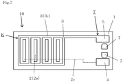
- Fig. 2 is a cross-sectional view of a sensor board 10 according to a second embodiment of the present invention.
- negative electrodes 3 include a peripheral portion 3c along the periphery of an insulating substrate 1 in a plan view.
- Positive electrodes 2 are arranged adjacent to the negative electrodes 3 within (or inward from) the area defined by the peripheral portion 3c.
- the positive electrodes 2 and the negative electrodes 3 adjacent to each other are linear (line segments), and are arranged in a line width direction.
- the negative electrodes 3 each have a line width smaller than the line width of each positive electrode 2. More specifically, the negative electrodes 3 are smaller than the positive electrodes 2 in a plan view.
- the negative electrodes 3 each have a relatively small line width. This effectively increases the density of the detection electrode K arranged on the insulating substrate 1.
- the sensor board 10 can thus be downsized and improve detection accuracy.
- the peripheral portion 3c in the negative electrodes 3 may have substantially the same line width. Thus, the peripheral portion 3c located on the upper or lower surface of the insulating substrate 1 easily allows the insulating substrate 1 to remain small in a plan view.
- the detection electrode K including the positive electrodes 2 and the negative electrodes 3 can maintain the electrode function for a longer period of time. More specifically, the electric field between the positive and negative electrodes 2 and 3 may cause electrochemical migration between the electrodes. When electrochemical migration occurs, metal ions move from the positive electrodes 2 and are deposited onto the negative electrodes 3, possibly causing defects such as voids in the positive electrodes 2. However, such defects constitute a relatively small volume percentage in the positive electrodes 2 having a relatively large area (volume or thickness).
- This structure can reduce deterioration of the function of the positive electrodes 2, and thus reduces possible electrode function deterioration of the detection electrode K, or more specifically, the function of, for example, detecting electrical short circuits between the positive electrodes 2 and the negative electrodes 3 caused by adhering particulate matter.
- the negative electrodes 3 include the peripheral portion 3c, which effectively attracts positively-charged particulate matter, such as soot, to the periphery of the insulating substrate 1. More specifically, the sensor board 10 can more efficiently adsorb, for example, soot in the surrounding environment.
- the peripheral portion 3c located along the periphery of the upper surface of the insulating substrate 1 defines a large area including the entire area in which the detection electrode K is located. Thus, the sensor board 10 effectively attracts and adsorbs, for example, soot.
- the multiple positive electrodes 2 are electrically connected to a positive electrode terminal 4 with a connection wire 2c inside the insulating substrate 1.
- Each positive electrode 2 is electrically connected to the connection wire 2c with a feedthrough conductor (not shown) extending through the insulating substrate 1 in the thickness direction from the positive electrode 2 to the connection wire 2c.
- the multiple negative electrodes 3 are electrically connected to a negative electrode terminal 5 with the peripheral portion 3c. The two ends of each negative electrode 3 are directly connected to the peripheral portion 3c. The negative electrodes 3 are thus electrically connected to the peripheral portion 3c.
- the multiple positive electrodes 2 or the multiple negative electrodes 3 included in the detection electrode K are electrically connected to the single positive electrode terminal 4 or the single negative electrode terminal 5 collectively.
- an electric potential can be easily applied to the multiple positive electrodes 2 and the multiple negative electrodes 3 in this example as well.
- each negative electrode 3 surrounds the corresponding positive electrode 2 in a frame together with a part of the peripheral portion 3 in a plan view.
- the negative electrodes 3 and the positive electrodes 2 in such a surrounding pattern can be easily electrically short-circuited by the particulate matter, such as soot, which tends to adhere to or around the negative electrodes 3 on the surface of the insulating substrate 1.
- the sensor improves the detection accuracy (low-level detection) of, for example, soot in the environment.
- the negative electrodes 3 may not be connected to the peripheral portion 3c at their two ends.
- the linear negative electrodes 3 may be connected to the peripheral portion 3c at one of the two ends to allow electrical connection between the negative electrodes 3 and the negative electrode terminal 5 through the peripheral portion 3c.
- Each negative electrode 3 can receive an electric potential from the negative electrode terminal 5 to adsorb, for example, soot.
- the peripheral portion 3c, the feed-through conductors, and the connection wire 2c are formed from the same metal material and in the same manner as the detection electrode K and the connection terminal T in the example shown in Figs. 1A and 1B .
- the feed-through conductors may be formed by filling, with a metal paste, through-holes in a ceramic green sheet to be the insulating substrate 1 and firing the resultant sheet.
- the through-holes may be formed by die machining or punching, for example, with laser.
- the feed-through conductors and the connection wire 2c which will not be exposed in a high-temperature environment, may be formed from the same metal material as the connection terminal T.
- the upper ends or other portions of the feed-through conductors for connection with the positive electrodes 3 are at relatively a small distance from the positive electrodes 3.
- the ends, or the upper ends, of the feed-through conductors may be formed from, for example, a metal material for easily forming a passivation layer, similarly to the detection electrode K.
- Fig. 3A is a plan view of a sensor board 10 according to a third embodiment of the present invention
- Fig. 3B is a cross-sectional view taken along line B-B in Fig. 3A
- the same components as in Figs. 1A and 1B are given the same reference numerals.
- the detection electrode K includes columnar positive electrodes 2A and columnar negative electrodes 3A.
- the detection electrode K as columnar conductors is, for example, feed-through conductors extending partially through the insulating substrate 1 from the upper surface in the thickness direction.
- the columnar conductors are, for example, cylindrical.
- each negative electrode 3A has a smaller diameter than each positive electrode 2A.
- the negative electrodes 3 each have a relatively small diameter. This effectively increases the density of the detection electrode K arranged on the insulating substrate 1.
- the sensor board 10 can thus be downsized and improve detection accuracy.
- the positive electrodes each have a relatively large diameter. This can reduce possible electrode function deterioration of the detection electrode K, similarly to the interdigitated electrode described above.
- each circular negative electrode 3A is, for example, about 50 to 80 ⁇ m.
- the diameter of each circular positive electrode 2A is, for example, about 100 to 120 ⁇ m, which is about 1.5 to 2 times the negative electrode 3A.
- connection terminal T The columnar positive electrodes 2 and the columnar negative electrodes 3 are electrically connected to connection terminal T with, for example, circuit-like inner wires (not shown) inside the insulating substrate 1.
- the inner wires connected to the positive electrodes 2A or the negative electrodes 3A are electrically connected to the connection terminal T with connection conductors 4a or 5a located on the upper surface of the insulating substrate 1 for connection with corresponding positive or negative electrodes.
- the connection conductors 4a and 5a extend, on the upper surface of the insulating substrate 1, from adjacent to the area in which the detection electrode K is arranged to the connection terminal T.
- the multiple positive electrodes 2A and the multiple negative electrodes 3A in the detection electrode K that are circular in a plan view as in the example in Fig. 3A can use a smaller area on the upper surface of the insulating substrate 1.
- more pairs of adjacent positive and negative electrodes 2A and 3A can be arranged easily, or an area for electrode pairs can be easily smaller.
- the sensor board 10 can thus be downsized and improve detection accuracy effectively.
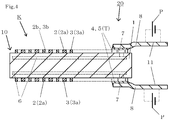
- the sensor board 1 with the above structure and direct current (DC) power sources P connected to the connection terminals T mainly form a sensor device 20 according to an embodiment of the present invention.
- the DC power sources P are schematically shown using circuit symbols.
- the connection terminal T in the sensor board 10 is electrically connected to the power source terminals in the DC power sources P with lead terminals 8.
- the lead terminals 8 connected to the positive electrode terminals 4 are connected to the positive power source terminals, whereas the lead terminals 8 connected to the negative electrode terminals 5 are connected to the negative power source terminals.
- the lead terminals 8 are not directly used to detect particulate matter, such as soot.
- the lead terminals 8 may be formed from any material appropriately selected in accordance with the surrounding environment, the yield and the economy of the sensor board 10, or other conditions.
- the lead terminals 8 are formed from a metal material highly resistant to oxidation such as platinum or gold, the sensor device 10 including the lead terminals 8 can be more reliable.
- the lead terminals 8 may also be formed from, for example, an iron-based alloy, such as an iron-nickel-cobalt alloy, or copper for economy.
- the lead terminals 8 formed from an iron-based alloy may have their outer surfaces protected with plating layers, such as gold plating layers (not shown).
- the lead terminals 8 are joined to the connection terminal T with, for example, a brazing material (with no labels) such as a silver brazing material (silver-copper brazing material) or a gold brazing material.
- a brazing material such as a silver brazing material (silver-copper brazing material) or a gold brazing material.
- the brazing material may be any material appropriately selected in accordance with various conditions for either manufacturing or using the sensor board 10 and the sensor device 20.
- the sensor device 20 can detect a decrease in electrical insulation or detect electrical short circuits between the positive electrodes 2 and the negative electrodes 3, or more specifically, adhering soot or other matter with a detector, such as a multimeter, connected between a pair of positive and negative lead terminals 8.
- the detector is, for example, an ammeter.
- An ammeter is connected to allow passage of a current when the positive electrodes 2 and the negative electrodes 3 are electrically short-circuited.
- a DC power source P and an ammeter may be sequentially connected in series between a pair of positive and negative lead terminals 8.
- the sensor device according to the embodiment of the present invention can be downsized and improve detection accuracy, in the same manner as the sensor board according to each embodiment described above.
- the detection electrode K on the upper surface of the insulating substrate 1 and the detection electrode K on the lower surface of the insulating substrate 1 may have different shapes and may be arranged differently in a manner to have, for example, different intervals between adjacent positive and negative electrodes.
- the detection electrode K may be arranged on side surfaces of the rectangular insulating substrate 1 along the long sides or on side surfaces along the short sides (end faces) in a plan view, rather than on the upper and lower surfaces.
- circular positive and negative electrodes may be located in the area surrounded by the peripheral portion 3.
- the peripheral portion 3c can effectively attract particulate matter, such as soot, in the environment.
- the positive electrodes and the negative electrodes arranged relatively densely can effectively adsorb the attracted soot onto the surface of the insulating substrate 1.
- the interval between adjacent positive and negative electrodes 2 and 3 may differ from the interval between other adjacent positive and negative electrodes 2 and 3.
- adhering soot or other matter can be detected readily in areas including electrodes at smaller intervals, whereas adhering soot or other matter can be detected over a longer period of time in areas including electrodes at larger intervals.
- the circular positive electrodes 2A and the circular negative electrodes 3A may be arranged in a manner other than in a grid pattern as in the example in Fig. 3A , and may include adjacent electrodes shifted diagonally (in a diagonal grid pattern). In this case, adjacent positive and negative electrodes 2A and 3A can be arranged at a smaller distance.
Landscapes
- Chemical & Material Sciences (AREA)
- Biochemistry (AREA)
- Physics & Mathematics (AREA)
- Health & Medical Sciences (AREA)
- Life Sciences & Earth Sciences (AREA)
- Analytical Chemistry (AREA)
- General Health & Medical Sciences (AREA)
- General Physics & Mathematics (AREA)
- Immunology (AREA)
- Pathology (AREA)
- Dispersion Chemistry (AREA)
- Chemical Kinetics & Catalysis (AREA)
- Electrochemistry (AREA)
- Investigating Or Analyzing Materials By The Use Of Electric Means (AREA)
Applications Claiming Priority (2)
| Application Number | Priority Date | Filing Date | Title |
|---|---|---|---|
| JP2017161960 | 2017-08-25 | ||
| PCT/JP2018/031169 WO2019039549A1 (ja) | 2017-08-25 | 2018-08-23 | センサ基板およびそれを備えるセンサ装置 |
Publications (2)
| Publication Number | Publication Date |
|---|---|
| EP3674700A1 true EP3674700A1 (de) | 2020-07-01 |
| EP3674700A4 EP3674700A4 (de) | 2021-05-12 |
Family
ID=65439005
Family Applications (1)
| Application Number | Title | Priority Date | Filing Date |
|---|---|---|---|
| EP18847958.8A Withdrawn EP3674700A4 (de) | 2017-08-25 | 2018-08-23 | Sensorsubstrat und damit versehene sensorvorrichtung |
Country Status (4)
| Country | Link |
|---|---|
| US (1) | US20200182768A1 (de) |
| EP (1) | EP3674700A4 (de) |
| JP (1) | JP6923657B2 (de) |
| WO (1) | WO2019039549A1 (de) |
Family Cites Families (13)
| Publication number | Priority date | Publication date | Assignee | Title |
|---|---|---|---|---|
| DE502004004590D1 (de) * | 2004-09-09 | 2007-09-20 | Analyticon Biotechnologies Ag | Lateralflussmessvorrichtung und Messverfahren für Analyten |
| JP4732902B2 (ja) * | 2006-01-18 | 2011-07-27 | セイコーインスツル株式会社 | 湿度センサおよびそれを有する半導体装置 |
| GB0601703D0 (en) * | 2006-01-27 | 2006-03-08 | Intellitect Water Ltd | Improvement To The Design And Construction Of Electrochemical Sensors |
| DE102006055520A1 (de) * | 2006-11-24 | 2008-05-29 | Robert Bosch Gmbh | Vorrichtung und Verfahren zur Überprüfung der Funktionsfähigkeit bzw. zur Plausibilisierung eines auf einem interdigitalen Elektrodensystem basierenden Sensors sowie ein Sensor zur Detektion von Teilchen in einem Gasstrom und dessen Verwendung |
| JP4898902B2 (ja) * | 2007-03-27 | 2012-03-21 | 日本碍子株式会社 | 微粒子センサ |
| JP5327152B2 (ja) * | 2010-07-05 | 2013-10-30 | 株式会社デンソー | 粒子状物質検出センサ素子及び粒子状物質検出センサ |
| JP5542006B2 (ja) | 2010-08-26 | 2014-07-09 | 日本碍子株式会社 | 粒子状物質検出装置 |
| JP5709808B2 (ja) | 2012-08-02 | 2015-04-30 | 株式会社日本自動車部品総合研究所 | 粒子状物質検出素子の製造方法、並びに、粒子状物質検出センサ |
| JP2014041009A (ja) * | 2012-08-21 | 2014-03-06 | Aisan Ind Co Ltd | 液位検出装置 |
| CN104614401B (zh) * | 2013-11-05 | 2017-12-29 | 中芯国际集成电路制造(上海)有限公司 | 气体传感器及其形成方法 |
| JP2016099169A (ja) * | 2014-11-19 | 2016-05-30 | 株式会社デンソー | 粒子状物質検出センサ |
| JP6425993B2 (ja) * | 2014-12-23 | 2018-11-21 | 株式会社Soken | 粒子状物質検出素子 |
| US9964481B2 (en) * | 2015-09-04 | 2018-05-08 | Ford Global Technologies, Llc | Method and system for exhaust particulate matter sensing |
-
2018
- 2018-08-23 JP JP2019537680A patent/JP6923657B2/ja active Active
- 2018-08-23 US US16/641,274 patent/US20200182768A1/en not_active Abandoned
- 2018-08-23 EP EP18847958.8A patent/EP3674700A4/de not_active Withdrawn
- 2018-08-23 WO PCT/JP2018/031169 patent/WO2019039549A1/ja not_active Ceased
Also Published As
| Publication number | Publication date |
|---|---|
| JP6923657B2 (ja) | 2021-08-25 |
| WO2019039549A1 (ja) | 2019-02-28 |
| US20200182768A1 (en) | 2020-06-11 |
| EP3674700A4 (de) | 2021-05-12 |
| JPWO2019039549A1 (ja) | 2020-09-17 |
Similar Documents
| Publication | Publication Date | Title |
|---|---|---|
| US9528971B2 (en) | Particulate matter detection element and method of manufacturing same | |
| CN107430053B (zh) | 用于检测导电和/或可极化粒子的传感器、传感器系统、用于操作传感器的方法、此类型传感器的制造方法以及此类型传感器用途 | |
| JP6228018B2 (ja) | 粒子状物質検出素子、粒子状物質検出センサ並びに粒子状物質検出素子の製造方法 | |
| EP3330702B1 (de) | Sensorsubstrat und sensorvorrichtung | |
| EP3187863B1 (de) | Sensorsubstrat, sensorsubstrat mit einer leitung und sensorvorrichtung | |
| EP3647777B1 (de) | Sensorsubstrat und sensorvorrichtung | |
| CN114041194A (zh) | Ntc薄膜热敏电阻和制造ntc薄膜热敏电阻的方法 | |
| CN104685340A (zh) | 用于探测微粒的传感器 | |
| JP2019158554A (ja) | センサ素子及びガスセンサ | |
| US5554839A (en) | Ceramic heater | |
| EP3674700A1 (de) | Sensorsubstrat und damit versehene sensorvorrichtung | |
| EP3460430B1 (de) | Temperatursensor und temperaturmessvorrichtung | |
| JP2004004072A (ja) | 測定センサ | |
| CN108369203A (zh) | 传感器元件用电极及传感器元件 | |
| JP2016099169A (ja) | 粒子状物質検出センサ | |
| EP3450945B1 (de) | Sensorsubstrat und sensorvorrichtung | |
| JP6503086B2 (ja) | センサ基板および検出モジュール | |
| JP2681301B2 (ja) | 検出素子端子構造 | |
| CN210198910U (zh) | 用于气体颗粒物浓度测量的芯片及传感器 | |
| KR102380365B1 (ko) | 측정 가스 챔버 내의 측정 가스의 입자를 검출하는 센서 소자 | |
| CN108431588A (zh) | 粒子状物质的测量装置用部件 | |
| JPS6286802A (ja) | リード線付セラミック体の製造方法 | |
| JP2010097791A (ja) | 過電圧保護部品 | |
| JP2018025564A (ja) | 粒子状物質検出素子 |
Legal Events
| Date | Code | Title | Description |
|---|---|---|---|
| STAA | Information on the status of an ep patent application or granted ep patent |
Free format text: STATUS: THE INTERNATIONAL PUBLICATION HAS BEEN MADE |
|
| PUAI | Public reference made under article 153(3) epc to a published international application that has entered the european phase |
Free format text: ORIGINAL CODE: 0009012 |
|
| STAA | Information on the status of an ep patent application or granted ep patent |
Free format text: STATUS: REQUEST FOR EXAMINATION WAS MADE |
|
| 17P | Request for examination filed |
Effective date: 20200225 |
|
| AK | Designated contracting states |
Kind code of ref document: A1 Designated state(s): AL AT BE BG CH CY CZ DE DK EE ES FI FR GB GR HR HU IE IS IT LI LT LU LV MC MK MT NL NO PL PT RO RS SE SI SK SM TR |
|
| AX | Request for extension of the european patent |
Extension state: BA ME |
|
| DAV | Request for validation of the european patent (deleted) | ||
| DAX | Request for extension of the european patent (deleted) | ||
| A4 | Supplementary search report drawn up and despatched |
Effective date: 20210413 |
|
| RIC1 | Information provided on ipc code assigned before grant |
Ipc: G01N 27/04 20060101AFI20210407BHEP Ipc: G01N 15/06 20060101ALI20210407BHEP |
|
| STAA | Information on the status of an ep patent application or granted ep patent |
Free format text: STATUS: THE APPLICATION IS DEEMED TO BE WITHDRAWN |
|
| 18D | Application deemed to be withdrawn |
Effective date: 20211116 |