EP3673380B1 - Einzeln adressierbare speichervorrichtungen, die von einem datenbus getrennt sind - Google Patents
Einzeln adressierbare speichervorrichtungen, die von einem datenbus getrennt sind Download PDFInfo
- Publication number
- EP3673380B1 EP3673380B1 EP18848839.9A EP18848839A EP3673380B1 EP 3673380 B1 EP3673380 B1 EP 3673380B1 EP 18848839 A EP18848839 A EP 18848839A EP 3673380 B1 EP3673380 B1 EP 3673380B1
- Authority
- EP
- European Patent Office
- Prior art keywords
- memory
- contact
- memory device
- command
- contacts
- Prior art date
- Legal status (The legal status is an assumption and is not a legal conclusion. Google has not performed a legal analysis and makes no representation as to the accuracy of the status listed.)
- Active
Links
Images

Classifications
-
- G—PHYSICS
- G06—COMPUTING OR CALCULATING; COUNTING
- G06F—ELECTRIC DIGITAL DATA PROCESSING
- G06F13/00—Interconnection of, or transfer of information or other signals between, memories, input/output devices or central processing units
- G06F13/14—Handling requests for interconnection or transfer
- G06F13/16—Handling requests for interconnection or transfer for access to memory bus
- G06F13/1668—Details of memory controller
-
- G—PHYSICS
- G06—COMPUTING OR CALCULATING; COUNTING
- G06F—ELECTRIC DIGITAL DATA PROCESSING
- G06F13/00—Interconnection of, or transfer of information or other signals between, memories, input/output devices or central processing units
- G06F13/14—Handling requests for interconnection or transfer
- G06F13/16—Handling requests for interconnection or transfer for access to memory bus
- G06F13/1668—Details of memory controller
- G06F13/1694—Configuration of memory controller to different memory types
-
- G—PHYSICS
- G06—COMPUTING OR CALCULATING; COUNTING
- G06F—ELECTRIC DIGITAL DATA PROCESSING
- G06F1/00—Details not covered by groups G06F3/00 - G06F13/00 and G06F21/00
- G06F1/26—Power supply means, e.g. regulation thereof
- G06F1/32—Means for saving power
- G06F1/3203—Power management, i.e. event-based initiation of a power-saving mode
- G06F1/3206—Monitoring of events, devices or parameters that trigger a change in power modality
-
- G—PHYSICS
- G06—COMPUTING OR CALCULATING; COUNTING
- G06F—ELECTRIC DIGITAL DATA PROCESSING
- G06F1/00—Details not covered by groups G06F3/00 - G06F13/00 and G06F21/00
- G06F1/26—Power supply means, e.g. regulation thereof
- G06F1/32—Means for saving power
- G06F1/3203—Power management, i.e. event-based initiation of a power-saving mode
- G06F1/3234—Power saving characterised by the action undertaken
- G06F1/325—Power saving in peripheral device
- G06F1/3275—Power saving in memory, e.g. RAM, cache
-
- G—PHYSICS
- G06—COMPUTING OR CALCULATING; COUNTING
- G06F—ELECTRIC DIGITAL DATA PROCESSING
- G06F1/00—Details not covered by groups G06F3/00 - G06F13/00 and G06F21/00
- G06F1/26—Power supply means, e.g. regulation thereof
- G06F1/32—Means for saving power
- G06F1/3203—Power management, i.e. event-based initiation of a power-saving mode
- G06F1/3234—Power saving characterised by the action undertaken
- G06F1/3296—Power saving characterised by the action undertaken by lowering the supply or operating voltage
-
- G—PHYSICS
- G06—COMPUTING OR CALCULATING; COUNTING
- G06F—ELECTRIC DIGITAL DATA PROCESSING
- G06F13/00—Interconnection of, or transfer of information or other signals between, memories, input/output devices or central processing units
- G06F13/14—Handling requests for interconnection or transfer
- G06F13/16—Handling requests for interconnection or transfer for access to memory bus
- G06F13/1668—Details of memory controller
- G06F13/1678—Details of memory controller using bus width
-
- G—PHYSICS
- G06—COMPUTING OR CALCULATING; COUNTING
- G06F—ELECTRIC DIGITAL DATA PROCESSING
- G06F5/00—Methods or arrangements for data conversion without changing the order or content of the data handled
- G06F5/06—Methods or arrangements for data conversion without changing the order or content of the data handled for changing the speed of data flow, i.e. speed regularising or timing, e.g. delay lines, FIFO buffers; over- or underrun control therefor
-
- G—PHYSICS
- G06—COMPUTING OR CALCULATING; COUNTING
- G06F—ELECTRIC DIGITAL DATA PROCESSING
- G06F2213/00—Indexing scheme relating to interconnection of, or transfer of information or other signals between, memories, input/output devices or central processing units
- G06F2213/0062—Bandwidth consumption reduction during transfers
Definitions
- US 2007/0161264 A1 relates to a memory system capable of changing the configuration of memory modules.
- the present disclosure generally relates to memory devices and, more particularly, relates to methods for individually addressing memory devices disconnected from a data bus and memory devices employing the same.
- Memory modules can include multiple memory devices for providing storage or working memory to a connected host device.
- Memory modules are frequently provided with a connector (e.g ., the edge connector of a dual inline memory module (DIMM)), in which a number of command/address contacts are shared by the memory devices, and a number of data contacts are uniquely coupled to data contacts on the memory devices.
- the number of data contacts on the connector of a memory module usually corresponds to the data bus width of the memory module.
- Different memory controllers are configured with support for different data bus widths, and are usually connected to memory modules with a data bus width that matches that of the memory controller.
- a memory module has a greater data bus width than a data bus width of a controller to which it is connected, some of the memory devices on the memory module may not be connected to the data bus of the memory controller.
- this arrangement prevent data transfer to and from the memory devices on the memory module that lack a data connection to the controller, but as memory devices may rely upon signals received at the data contacts thereof to individually target the memory devices for various commands (e.g ., a command to enter a reduced-power mode, to change termination impedance, etc.), this arrangement prevents communication of targeted commands to the memory devices so disconnected. Accordingly, a way to individually target memory devices on a memory module for particular commands, even in the absence of a data connection to a memory controller, are desired.
- a memory device comprises a memory array, at least one command contact, and at least one data contact.
- the memory device is configured to detect a condition in which the at least one command contact is connected to a controller and the at least one data contact is disconnected from the controller, and in response to the detected condition, enter a reduced-power mode.
- FIG. 1 schematically illustrates a memory module 100 including a plurality of memories 120 (e.g ., memory dies, memory chips, memory packages or the like) in accordance with an embodiment of the present invention.
- the module 100 includes an edge connector 130 with a number of connector contacts 132 (e.g ., connector data contacts 134 and connector command/address contacts 136) along an edge of a substrate 101 ( e.g ., a printed circuit board (PCB) or the like) of the module 100 for connecting a data bus 104 and a command/address bus 106 to a host device.
- the data bus 104 connects the memories 120 to the edge connector 130 and receives data signals from and transmits data signals to a connected host during memory access operations (e.
- the module 100 can further include control circuitry (e.g ., including a registering clock driver (RCD) 190) that receives command/address signals from the command/address bus 106 and generates memory command/address signals for the memories 120.
- the RCD 190 can present a predictable electrical load (e.g ., for matching impedance, reactance, capacitance, etc. ) to the host device and can re-drive memory command/address signals to the memories 120, which helps enable higher densities and increase signal integrity.
- the RCD 190 may also buffer the command/address signals provided by the host, and then transmit the buffered signals as memory command/address signals to the memories 120.
- Each of the memories 120 can include a plurality of memory regions, which can each include a plurality of memory cells.
- the memories 120 can be individual memory dies, memory planes in a single memory die, a stack of memory dies vertically connected with through-silicon vias (TSVs), or the like.
- TSVs through-silicon vias
- each of the memories can be formed from a semiconductor die and arranged with other memory dies in a single device package (not shown).
- multiple memories 120 can be co-located on a single die and/or distributed across multiple device packages.
- the memory cells can include, for example, volatile memory cells, such as DRAM or SRAM cells.
- floating gate, charge trap, phase change, ferroelectric, magnetoresistive, and/or other suitable storage elements configured to store data persistently or semi-persistently.
- the memories 120 can also include other circuit components (not shown), such as multiplexers, decoders, buffers, read/write drivers, address registers, data out/data in registers, etc., for accessing and/or programming ( e.g ., writing) the memory cells and other functionality, such as for processing information and/or communicating with a connected controller.
- Each of the memories 120 can include a number of data contacts 124 and a number of command/address contacts 126.
- Each of the connector command/address contacts 136 can be connected to one or more of the command/address contacts 126 ( e.g ., in either a one-to-one arrangement or a one-to-many arrangement).
- the connector command/address contacts 136 can include one or more command contacts, such as strobe contacts (e.g ., row access strobe (RAS), column access strobe (CAS), data strobes (DQS), etc.), clock contacts ( e.g ., CK, CK#), enable contacts ( e.g ., clock enable (CKE), chip enable (CE), bank enable (BE), write enable (WE), etc. ) , masks ( e.g ., data mask (DM), etc. ) , address contacts ( e.g ., row address, column address, bank address, etc .) , and the like, as is well known to those skilled in the art.
- strobe contacts e.g ., row access strobe (RAS), column access strobe (CAS), data strobes (DQS), etc.
- clock contacts e.g ., CK, CK#
- enable contacts e.g ., clock enable (CKE), chip enable
- the connector contacts 132 can further include power and ground contacts, which may in some embodiments be included in the command/address contacts 136, and in other embodiments may be considered as separate contacts.
- Each of the connector data contacts 134 can be connected to a separate one of the data contacts 124 ( e.g ., in a one-to-one arrangement).
- the number of data contacts 124 is thus equal to the number of connector data contacts in the module, and represents a width of the data bus 104 that can be utilized to provide data to and from all of the memories 120.
- Different memory controllers may be provided with different data bus widths, and it may be desirable for a memory module to be optimized for use with multiple different memory controller designs.
- a DDR4 memory controller may have a data bus width of 72 bits (e.g ., corresponding to nine memories 120 with four data contacts 124 each), while a DDR5 memory controller may have a larger data bus width (e.g ., 80 bits, corresponding to ten memories 120 with four data contacts 124 each). If a memory module has more connector data contacts 134 than the controller to which it is connected has data bus width, some of the memories 120 may have data contacts 124 that are inaccessible to the controller.
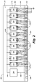
- FIG. 2 illustrates a memory module 200 including a plurality of memories 220 in accordance with an embodiment of the present invention.
- the module 200 includes an edge connector 230 with a number of connector contacts 232 (e.g ., connector data contacts 234 and connector command/address contacts 236) along an edge of a substrate 201 ( e.g ., a printed circuit board (PCB) or the like) of the module 200 for connecting a data bus 204 and a command/address bus 206 to a host device.
- the data bus 204 connects the memories 220 to the edge connector 230 and receives data signals from and transmits data signals to a connected host during memory access operations ( e.g. , reads and writes).
- the module 200 can further include control circuitry (e.g ., including a registering clock driver (RCD) 290) that receives command/address signals from the command/address bus 206 and generates memory command/address signals for the memories 220.
- the RCD 290 can present a predictable electrical load (e.g ., for matching impedance, reactance, capacitance, etc .) to the host device and can re-drive memory command/address signals to the memories 220, which helps enable higher densities and increase signal integrity.
- the RCD 290 may also buffer the command/address signals provided by the host, and then transmit the buffered signals as memory command/address signals to the memories 220.
- Each of the memories 220 can include a number of data contacts 224 and a number of command/address contacts 226.
- Each of the connector command/address contacts 236 can be connected to one or more of the command/address contacts 226 ( e.g ., in either a one-to-one arrangement or a one-to-many arrangement).
- the connector command/address contacts 236 can include one or more command contacts, such as strobe contacts (e.g ., row access strobe (RAS), column access strobe (CAS), data strobes (DQS), etc.
- strobe contacts e.g ., row access strobe (RAS), column access strobe (CAS), data strobes (DQS), etc.
- the connector contacts 232 can further include power and ground contacts, which may in some embodiments be included in the connector command/address contacts 236, and in other embodiments may be considered as separate contacts.
- Each of the connector data contacts 234 can be connected to a separate one of the data contacts 224 ( e.g ., in a one-to-one arrangement).
- the number of data contacts 224 is thus equal to the number of connector data contacts in the module, and represents a width of the data bus 204 that can be utilized to provide data to and from all of the memories 220.
- the connector data contacts 234 for which no data bus lines is available can be connected to a common ground (e.g ., rather than being left to float).
- a controller e.g ., via edge connector 230
- the connector data contacts 234 for which no data bus lines is available can be connected to a common ground (e.g ., rather than being left to float).
- PDA per-DRAM addressability
- the disconnection of the data contacts 224 from the controller renders the memory 220 so disconnected un-addressable for a PDA command.
- Connecting the connector data contacts 234 for which no connection to the controller is available (e.g ., due to the limited data bus width of the controller) to a common ground can allow the memory 220 coupled to these connector data contacts 234 to detect that it is not individually addressable by the controller (e.g ., even though the command/address bus 206 is still connected to the memory 220 by the shared and/or unique command/address connector contacts 236).
- the memory 220 so disconnected from the controller can be configured to place itself into a reduced-power state (e.g ., a state in which the memory 220 no longer actively "listens" to the command/address bus 206).
- the reduced-power state which may also be referred to as a reduced-power mode, is thus a first operating mode with a lower nominal power rating, power requirement, power usage, or power draw than a second operating mode.
- a first operating mode is the reduced-power mode and a second operating mode may be a normal, typical, or full-power mode
- the memory 220 can be configured with circuitry to detect a condition in which a controller is connected to the command/address contacts 226 of the memory 220, and the data contacts 224 of the memory 220 are disconnected from the controller.
- One such circuit can be configured to detect a "reset" signal on the command/address bus 206 simultaneously with ( e.g ., or shortly before or shortly after) the voltage on the data contacts 224 of the memory are determined to be held low ( e.g ., below a reference voltage level).
- the memory 220 can be configured to detect a condition in which a controller is connected to the command/address contacts 226 of the memory 220, and the data contacts 224 of the memory 220 are disconnected from the controller by exploiting the independently addressable command/address contacts 226 on the memory 220.
- a controller can be configured to hold these two connections at opposing high and low values (rather than strobing them complementarily).
- the memory 220 may be configured to evaluate the FIFO counter to determine if the value thereof is below a predetermined threshold. Such a determination, possibly in combination with another signal on the command/address bus (e.g ., a "reset" command or a PDA command), can trigger the memory 220 to enter a reduced-power mode.
- a signal on the command/address bus e.g ., a "reset" command or a PDA command
- memory devices have been described as entering a reduced-power mode in response to detecting a condition in which the memory devices are connected by a command/address bus to a controller, but disconnected from the data bus thereof, in other embodiments, such a detection can trigger other responses from the memory devices besides entering a reduced-power mode. For example, it may be desirable to send other commands to a memory device in a memory module that is not accessible via a data bus, such as commands to adjust an on-die termination level thereof ( e.g ., for impedance matching).
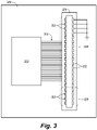
- FIG. 3 illustrates a memory system in accordance with one embodiment of the present invention.
- Memory system 300 includes a controller 310 and a memory interface 320 (e.g ., a DIMM slot) coupled to the memory controller ( e.g ., by memory bus 315).
- the memory interface 320 is configured to receive a connector of a memory device (e.g ., an edge connector of a DIMM).
- the memory interface 320 includes a plurality of memory interface contacts 322, including memory interface data contacts 324 and memory interface command/address contacts 326.
- the memory interface contacts 322 are configured to connect to connector contacts of the connector of the memory device.
- the memory interface command/address contacts 326 are configured to connect to connector command/address contacts of the memory device, and the memory interface data contacts 324 are configured to connect to connector data contacts of the memory device.
- One or more of the memory interface data contacts 324 can be electrically disconnected from the memory controller (e.g ., not connected to the memory bus 315), but instead coupled to a common electrical ground. As can be seen with reference to Figure 3 , four of the memory interface data contacts 324 have been grounded and disconnected from the memory bus 315 and from the controller 310.
- a memory interface 320 so configured can allow memory devices with different data bus widths to be connected to the same controller, and optimized for improved power consumption.
- grounding the data connects of a memory device can be used by the memory device (e.g ., one or more DRAM devices on a DIMM) to detect a condition in which data transfer between the memory device and the controller 310 is precluded.
- the memory device can enter a reduced-power state (or another mode, such as an on-die termination mode of one or more predetermined impedances) to reduce the power consumption of the memory system 300
- the memory system 300 can be connected to a host device, or be incorporated as part of a host device.
- the host device can be any one of a number of electronic devices capable of utilizing memory for the temporary or persistent storage of information, or a component thereof.
- host device may be a computing device such as a desktop or portable computer, a server, a hand-held device ( e.g ., a mobile phone, a tablet, a digital reader, a digital media player), or some component thereof ( e.g ., a central processing unit, a co-processor, a dedicated memory controller, etc. ) .
- the host device may be a networking device (e.g ., a switch, a router, etc.
- the host device may be connected directly to a memory module or a memory device, although in other embodiments, the host device may be indirectly connected to the memory module or the memory device ( e.g ., over a networked connection or through intermediary devices).
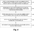
- Figure 4 is a flow chart illustrating a method of operating a memory device in accordance with an embodiment of the present invention.
- the method includes detecting a condition in which at least one command contact of the memory device is connected to a controller and at least one data contact is disconnected from the controller (box 410).
- the method further includes entering, based at least in part on detecting the condition, a first operating mode with a lower nominal power rating than a second operating mode (box 420).
- detecting the condition can include detecting a command signal (e.g ., a reset signal or the like) at the at least one command contact and determining that the at least one data contact is grounded. The detecting and determining can be performed simultaneously, or sequentially in either order.
- the at least one command contact includes a first strobe contact and a second strobe contact, and detecting the condition includes determining that the first and second strobe contacts are driven to opposing high and low levels.
- determining that the first and second strobe contacts are driven to opposing high and low levels can include determining that the FIFO counter is below a predetermined threshold.
- the method can optionally further include ignoring signals received at the at least one command contact while the memory device is in the first operating mode (box 430). Moreover, the method can optionally further include detecting a second condition in which the data contact is connected to the controller (box 440), and exiting, based at least in part on detecting the second condition, the first operating mode (box 450).
Landscapes
- Engineering & Computer Science (AREA)
- Theoretical Computer Science (AREA)
- Physics & Mathematics (AREA)
- General Engineering & Computer Science (AREA)
- General Physics & Mathematics (AREA)
- Techniques For Improving Reliability Of Storages (AREA)
- Read Only Memory (AREA)
- Power Sources (AREA)
Claims (15)
- Speichervorrichtung (220), die Folgendes umfasst:wenigstens einen Befehlskontakt (226); undwenigstens einen Datenkontakt (224),dadurch gekennzeichnet, dass die Speichervorrichtung konfiguriert ist zum:Detektieren eines Zustands, in dem der wenigstens eine Befehlskontakt mit einer Steuereinheit verbunden ist und der wenigstens eine Datenkontakt von der Steuereinheit getrennt ist, undEintreten in eine erste Betriebsart mit einer geringeren Nennleistung als in einer zweiten Betriebsart der Speichervorrichtung in Reaktion auf den detektierten Zustand.
- Speichervorrichtung nach Anspruch 1, wobei die Speichervorrichtung konfiguriert ist zum Detektieren des Zustands wenigstens teilweise anhand des Detektierens eines Befehlssignals an dem wenigstens einen Befehlskontakt und des Bestimmens, dass der wenigstens eine Datenkontakt mit Masse verbunden ist.
- Speichervorrichtung nach Anspruch 2, wobei das Befehlssignal ein Rücksetzsignal enthält.
- Speichervorrichtung nach Anspruch 1, wobei der wenigstens eine Befehlskontakt einen ersten Strobe-Kontakt und einen zweiten Strobe-Kontakt umfasst und wobei die Speichervorrichtung konfiguriert ist zum Detektieren des Zustands wenigstens teilweise anhand des Bestimmens, dass der erste und der zweite Strobe-Kontakt auf einen hohen und einen dazu entgegengesetzten tiefen Pegel angesteuert werden.
- Speichervorrichtung nach Anspruch 4, wobei der erste Strobe-Kontakt und der zweite Strobe-Kontakt mit einem ersten First-in/First-out-Zähler (FIFO-Zähler) gekoppelt sind und wobei das Bestimmen, dass der erste und der zweite Strobe-Kontakt auf einen hohen und einen dazu entgegengesetzten tiefen Pegel angesteuert werden, das Bestimmen, dass der FIFO-Zähler unter einem vorgegebenen Schwellenwert liegt, umfasst.
- Speichervorrichtung nach Anspruch 1, wobei die erste Betriebsart eine Betriebsart ist, in der die Speichervorrichtung konfiguriert ist zum Ignorieren von Signalen, die an dem wenigstens einen Befehlskontakt empfangen werden.
- Speichervorrichtung nach Anspruch 1, wobei der Zustand ein erster Zustand ist und wobei die Speichervorrichtung konfiguriert ist zum Verlassen der ersten Betriebsart wenigstens teilweise anhand des Detektierens eines zweiten Zustands, in dem der Datenkontakt mit der Steuereinheit verbunden ist.
- Verfahren zum Betreiben einer Speichervorrichtung (220), gekennzeichnet durch:Detektieren (410) eines Zustands, in dem wenigstens ein Befehlskontakt (226) der Speichervorrichtung mit einer Steuereinheit verbunden ist und wenigstens ein Datenkontakt (224) der Speichervorrichtung von der Steuereinheit getrennt ist; undEintreten (420) wenigstens teilweise anhand des Detektierens des Zustands in eine erste Betriebsart der Speichervorrichtung mit einer geringeren Nennleistung als in einer zweiten Betriebsart der Speichervorrichtung.
- Verfahren nach Anspruch 8, wobei das Detektieren des Zustands das Detektieren eines Befehlssignals an dem wenigstens einen Befehlskontakt und das Bestimmen, dass der wenigstens eine Datenkontakt mit Masse verbunden ist, umfasst.
- Verfahren nach Anspruch 9, wobei das Befehlssignal ein Rücksetzsignal umfasst.
- Verfahren nach Anspruch 8, wobei der wenigstens eine Befehlskontakt einen ersten Strobe-Kontakt und einen zweiten Strobe-Kontakt umfasst und wobei das Detektieren des Zustands das Bestimmen, dass der erste und der zweite Strobe-Kontakt auf einen hohen und einen dazu entgegengesetzten tiefen Pegel angesteuert werden, umfasst.
- Verfahren nach Anspruch 11, wobei der erste Strobe-Kontakt und der zweite Strobe-Kontakt mit einem First-in/First-out-Zähler (FIFO-Zähler) gekoppelt sind und wobei das Bestimmen, dass der erste und der zweite Strobe-Kontakt auf einen hohen und einen dazu entgegengesetzten tiefen Pegel angesteuert werden, das Bestimmen, dass der FIFO-Zähler unter einem vorgegebenen Schwellenwert liegt, umfasst.
- Verfahren nach Anspruch 8, das ferner das Ignorieren von Signalen, die an dem wenigstens einen Befehlskontakt empfangen werden, während die Speichervorrichtung in der ersten Betriebsart ist, umfasst.
- Verfahren nach Anspruch 8, wobei der Zustand ein erster Zustand ist, ferner umfassend:Detektieren eines zweiten Zustands, in dem der Datenkontakt mit der Steuereinheit verbunden ist; undVerlassen der ersten Betriebsart wenigstens teilweise anhand des Detektierens des zweiten Zustands.
- Speichermodul (200), das Folgendes umfasst:
mehrere Speicher (220), wovon jeder die Speichervorrichtung nach einem der Ansprüche 1-7 umfasst.
Applications Claiming Priority (3)
| Application Number | Priority Date | Filing Date | Title |
|---|---|---|---|
| US201762550483P | 2017-08-25 | 2017-08-25 | |
| US16/014,498 US10657081B2 (en) | 2017-08-25 | 2018-06-21 | Individually addressing memory devices disconnected from a data bus |
| PCT/US2018/042101 WO2019040200A1 (en) | 2017-08-25 | 2018-07-13 | INDIVIDUAL ADDRESSING OF MEMORY DEVICES DISCONNECTED FROM A DATA BUS |
Publications (3)
| Publication Number | Publication Date |
|---|---|
| EP3673380A1 EP3673380A1 (de) | 2020-07-01 |
| EP3673380A4 EP3673380A4 (de) | 2021-04-28 |
| EP3673380B1 true EP3673380B1 (de) | 2022-10-12 |
Family
ID=65434268
Family Applications (1)
| Application Number | Title | Priority Date | Filing Date |
|---|---|---|---|
| EP18848839.9A Active EP3673380B1 (de) | 2017-08-25 | 2018-07-13 | Einzeln adressierbare speichervorrichtungen, die von einem datenbus getrennt sind |
Country Status (5)
| Country | Link |
|---|---|
| US (5) | US10657081B2 (de) |
| EP (1) | EP3673380B1 (de) |
| KR (1) | KR102388247B1 (de) |
| CN (1) | CN111052098B (de) |
| WO (1) | WO2019040200A1 (de) |
Families Citing this family (4)
| Publication number | Priority date | Publication date | Assignee | Title |
|---|---|---|---|---|
| US10657081B2 (en) | 2017-08-25 | 2020-05-19 | Micron Technology, Inc. | Individually addressing memory devices disconnected from a data bus |
| US10388362B1 (en) * | 2018-05-08 | 2019-08-20 | Micron Technology, Inc. | Half-width, double pumped data path |
| US12278629B2 (en) * | 2022-05-19 | 2025-04-15 | Changxin Memory Technologies, Inc. | Delay circuit and memory |
| KR20250169702A (ko) * | 2024-05-27 | 2025-12-04 | 에스케이하이닉스 주식회사 | 반도체 장치 및 반도체 시스템 |
Family Cites Families (13)
| Publication number | Priority date | Publication date | Assignee | Title |
|---|---|---|---|---|
| US6321277B1 (en) * | 1998-11-16 | 2001-11-20 | International Business Machines Corporation | Separable in-line automatic terminator for use with a data processing system bus |
| US6460143B1 (en) * | 1999-05-13 | 2002-10-01 | Apple Computer, Inc. | Apparatus and method for awakening bus circuitry from a low power state |
| US6708278B2 (en) | 1999-06-28 | 2004-03-16 | Apple Computer, Inc. | Apparatus and method for awakening bus circuitry from a low power state |
| US7827348B2 (en) * | 2000-01-06 | 2010-11-02 | Super Talent Electronics, Inc. | High performance flash memory devices (FMD) |
| KR100761832B1 (ko) | 2006-01-09 | 2007-09-28 | 삼성전자주식회사 | 메모리 모듈의 구성을 변경할 수 있는 메모리 시스템 |
| US7848153B2 (en) | 2008-08-19 | 2010-12-07 | Qimonda Ag | High speed memory architecture |
| KR101737020B1 (ko) * | 2009-09-09 | 2017-05-29 | 마벨 월드 트레이드 리미티드 | 다중 파워서플라이들 및/또는 다중 저전력 모드들을 갖는 메모리 |
| CN102881319A (zh) * | 2011-07-14 | 2013-01-16 | 鸿富锦精密工业(深圳)有限公司 | 内存 |
| US9037890B2 (en) | 2012-07-26 | 2015-05-19 | Artemis Acquisition Llc | Ultra-deep power-down mode for memory devices |
| CN104102600B (zh) | 2013-04-03 | 2018-01-12 | 慧荣科技股份有限公司 | 存储器控制器 |
| TWI526818B (zh) | 2015-03-19 | 2016-03-21 | 群聯電子股份有限公司 | 休眠模式啓動方法、記憶體控制電路單元及儲存裝置 |
| US9804978B2 (en) * | 2015-03-30 | 2017-10-31 | Lenovo Enterprise Solutions (Singapore) Pte. Ltd. | Memory system facilitating high bandwidth and high capacity memory |
| US10657081B2 (en) | 2017-08-25 | 2020-05-19 | Micron Technology, Inc. | Individually addressing memory devices disconnected from a data bus |
-
2018
- 2018-06-21 US US16/014,498 patent/US10657081B2/en active Active
- 2018-07-13 KR KR1020207008535A patent/KR102388247B1/ko active Active
- 2018-07-13 WO PCT/US2018/042101 patent/WO2019040200A1/en not_active Ceased
- 2018-07-13 CN CN201880053634.XA patent/CN111052098B/zh active Active
- 2018-07-13 EP EP18848839.9A patent/EP3673380B1/de active Active
-
2020
- 2020-04-10 US US16/846,146 patent/US10754801B2/en active Active
- 2020-07-16 US US16/931,144 patent/US10983934B2/en active Active
-
2021
- 2021-03-19 US US17/207,561 patent/US11436169B2/en active Active
-
2022
- 2022-09-02 US US17/929,643 patent/US12367161B2/en active Active
Also Published As
| Publication number | Publication date |
|---|---|
| WO2019040200A1 (en) | 2019-02-28 |
| US20220414034A1 (en) | 2022-12-29 |
| US20210209039A1 (en) | 2021-07-08 |
| US20200242057A1 (en) | 2020-07-30 |
| EP3673380A1 (de) | 2020-07-01 |
| CN111052098B (zh) | 2023-07-28 |
| KR20200035326A (ko) | 2020-04-02 |
| US10754801B2 (en) | 2020-08-25 |
| US20200349097A1 (en) | 2020-11-05 |
| US11436169B2 (en) | 2022-09-06 |
| US10657081B2 (en) | 2020-05-19 |
| US20190065416A1 (en) | 2019-02-28 |
| US12367161B2 (en) | 2025-07-22 |
| US10983934B2 (en) | 2021-04-20 |
| EP3673380A4 (de) | 2021-04-28 |
| KR102388247B1 (ko) | 2022-04-19 |
| CN111052098A (zh) | 2020-04-21 |
Similar Documents
| Publication | Publication Date | Title |
|---|---|---|
| US12367161B2 (en) | Individually addressing memory devices disconnected from a data bus | |
| US20250045203A1 (en) | Selectively-activated termination circuitry, and associated systems, methods, and devices | |
| US9747230B2 (en) | Memory rank and ODT configuration in a memory system | |
| US11947474B2 (en) | Multi-mode memory module and memory component | |
| US20030126338A1 (en) | Memory bus termination with memory unit having termination control | |
| US10141314B2 (en) | Memories and methods to provide configuration information to controllers | |
| US9305625B2 (en) | Apparatuses and methods for unit identification in a master/slave memory stack | |
| US9747037B2 (en) | Extended-height DIMM | |
| US12182416B2 (en) | Memory device and memory system including the same | |
| US20240371410A1 (en) | Apparatus including multiple high bandwidth memory cubes | |
| US10976368B2 (en) | Memory apparatus relating to determination of a failed region and test method thereof, memory module and system using the same | |
| CN113889160B (zh) | 多寄存器时钟驱动器加载的存储器子系统 | |
| CN115344513B (zh) | 具有装置到控制器通信总线的存储器及相关联方法 | |
| US12437789B2 (en) | Apparatus with timing control for a die grouping | |
| US10355001B2 (en) | Memories and methods to provide configuration information to controllers |
Legal Events
| Date | Code | Title | Description |
|---|---|---|---|
| STAA | Information on the status of an ep patent application or granted ep patent |
Free format text: STATUS: THE INTERNATIONAL PUBLICATION HAS BEEN MADE |
|
| PUAI | Public reference made under article 153(3) epc to a published international application that has entered the european phase |
Free format text: ORIGINAL CODE: 0009012 |
|
| STAA | Information on the status of an ep patent application or granted ep patent |
Free format text: STATUS: REQUEST FOR EXAMINATION WAS MADE |
|
| 17P | Request for examination filed |
Effective date: 20200116 |
|
| AK | Designated contracting states |
Kind code of ref document: A1 Designated state(s): AL AT BE BG CH CY CZ DE DK EE ES FI FR GB GR HR HU IE IS IT LI LT LU LV MC MK MT NL NO PL PT RO RS SE SI SK SM TR |
|
| AX | Request for extension of the european patent |
Extension state: BA ME |
|
| DAV | Request for validation of the european patent (deleted) | ||
| DAX | Request for extension of the european patent (deleted) | ||
| A4 | Supplementary search report drawn up and despatched |
Effective date: 20210329 |
|
| RIC1 | Information provided on ipc code assigned before grant |
Ipc: G06F 13/16 20060101AFI20210323BHEP Ipc: G06F 1/3206 20190101ALI20210323BHEP |
|
| GRAP | Despatch of communication of intention to grant a patent |
Free format text: ORIGINAL CODE: EPIDOSNIGR1 |
|
| STAA | Information on the status of an ep patent application or granted ep patent |
Free format text: STATUS: GRANT OF PATENT IS INTENDED |
|
| INTG | Intention to grant announced |
Effective date: 20220429 |
|
| RIN1 | Information on inventor provided before grant (corrected) |
Inventor name: PRATHER, MATTHEW A. Inventor name: SCHAEFER, SCOTT E. |
|
| GRAS | Grant fee paid |
Free format text: ORIGINAL CODE: EPIDOSNIGR3 |
|
| GRAA | (expected) grant |
Free format text: ORIGINAL CODE: 0009210 |
|
| STAA | Information on the status of an ep patent application or granted ep patent |
Free format text: STATUS: THE PATENT HAS BEEN GRANTED |
|
| AK | Designated contracting states |
Kind code of ref document: B1 Designated state(s): AL AT BE BG CH CY CZ DE DK EE ES FI FR GB GR HR HU IE IS IT LI LT LU LV MC MK MT NL NO PL PT RO RS SE SI SK SM TR |
|
| REG | Reference to a national code |
Ref country code: GB Ref legal event code: FG4D |
|
| REG | Reference to a national code |
Ref country code: CH Ref legal event code: EP |
|
| REG | Reference to a national code |
Ref country code: DE Ref legal event code: R096 Ref document number: 602018041791 Country of ref document: DE |
|
| REG | Reference to a national code |
Ref country code: IE Ref legal event code: FG4D |
|
| REG | Reference to a national code |
Ref country code: AT Ref legal event code: REF Ref document number: 1524593 Country of ref document: AT Kind code of ref document: T Effective date: 20221115 |
|
| REG | Reference to a national code |
Ref country code: LT Ref legal event code: MG9D |
|
| REG | Reference to a national code |
Ref country code: NL Ref legal event code: MP Effective date: 20221012 |
|
| REG | Reference to a national code |
Ref country code: AT Ref legal event code: MK05 Ref document number: 1524593 Country of ref document: AT Kind code of ref document: T Effective date: 20221012 |
|
| PG25 | Lapsed in a contracting state [announced via postgrant information from national office to epo] |
Ref country code: NL Free format text: LAPSE BECAUSE OF FAILURE TO SUBMIT A TRANSLATION OF THE DESCRIPTION OR TO PAY THE FEE WITHIN THE PRESCRIBED TIME-LIMIT Effective date: 20221012 |
|
| PG25 | Lapsed in a contracting state [announced via postgrant information from national office to epo] |
Ref country code: SE Free format text: LAPSE BECAUSE OF FAILURE TO SUBMIT A TRANSLATION OF THE DESCRIPTION OR TO PAY THE FEE WITHIN THE PRESCRIBED TIME-LIMIT Effective date: 20221012 Ref country code: PT Free format text: LAPSE BECAUSE OF FAILURE TO SUBMIT A TRANSLATION OF THE DESCRIPTION OR TO PAY THE FEE WITHIN THE PRESCRIBED TIME-LIMIT Effective date: 20230213 Ref country code: NO Free format text: LAPSE BECAUSE OF FAILURE TO SUBMIT A TRANSLATION OF THE DESCRIPTION OR TO PAY THE FEE WITHIN THE PRESCRIBED TIME-LIMIT Effective date: 20230112 Ref country code: LT Free format text: LAPSE BECAUSE OF FAILURE TO SUBMIT A TRANSLATION OF THE DESCRIPTION OR TO PAY THE FEE WITHIN THE PRESCRIBED TIME-LIMIT Effective date: 20221012 Ref country code: FI Free format text: LAPSE BECAUSE OF FAILURE TO SUBMIT A TRANSLATION OF THE DESCRIPTION OR TO PAY THE FEE WITHIN THE PRESCRIBED TIME-LIMIT Effective date: 20221012 Ref country code: ES Free format text: LAPSE BECAUSE OF FAILURE TO SUBMIT A TRANSLATION OF THE DESCRIPTION OR TO PAY THE FEE WITHIN THE PRESCRIBED TIME-LIMIT Effective date: 20221012 Ref country code: AT Free format text: LAPSE BECAUSE OF FAILURE TO SUBMIT A TRANSLATION OF THE DESCRIPTION OR TO PAY THE FEE WITHIN THE PRESCRIBED TIME-LIMIT Effective date: 20221012 |
|
| PG25 | Lapsed in a contracting state [announced via postgrant information from national office to epo] |
Ref country code: RS Free format text: LAPSE BECAUSE OF FAILURE TO SUBMIT A TRANSLATION OF THE DESCRIPTION OR TO PAY THE FEE WITHIN THE PRESCRIBED TIME-LIMIT Effective date: 20221012 Ref country code: PL Free format text: LAPSE BECAUSE OF FAILURE TO SUBMIT A TRANSLATION OF THE DESCRIPTION OR TO PAY THE FEE WITHIN THE PRESCRIBED TIME-LIMIT Effective date: 20221012 Ref country code: LV Free format text: LAPSE BECAUSE OF FAILURE TO SUBMIT A TRANSLATION OF THE DESCRIPTION OR TO PAY THE FEE WITHIN THE PRESCRIBED TIME-LIMIT Effective date: 20221012 Ref country code: IS Free format text: LAPSE BECAUSE OF FAILURE TO SUBMIT A TRANSLATION OF THE DESCRIPTION OR TO PAY THE FEE WITHIN THE PRESCRIBED TIME-LIMIT Effective date: 20230212 Ref country code: HR Free format text: LAPSE BECAUSE OF FAILURE TO SUBMIT A TRANSLATION OF THE DESCRIPTION OR TO PAY THE FEE WITHIN THE PRESCRIBED TIME-LIMIT Effective date: 20221012 Ref country code: GR Free format text: LAPSE BECAUSE OF FAILURE TO SUBMIT A TRANSLATION OF THE DESCRIPTION OR TO PAY THE FEE WITHIN THE PRESCRIBED TIME-LIMIT Effective date: 20230113 |
|
| REG | Reference to a national code |
Ref country code: DE Ref legal event code: R097 Ref document number: 602018041791 Country of ref document: DE |
|
| PG25 | Lapsed in a contracting state [announced via postgrant information from national office to epo] |
Ref country code: SM Free format text: LAPSE BECAUSE OF FAILURE TO SUBMIT A TRANSLATION OF THE DESCRIPTION OR TO PAY THE FEE WITHIN THE PRESCRIBED TIME-LIMIT Effective date: 20221012 Ref country code: RO Free format text: LAPSE BECAUSE OF FAILURE TO SUBMIT A TRANSLATION OF THE DESCRIPTION OR TO PAY THE FEE WITHIN THE PRESCRIBED TIME-LIMIT Effective date: 20221012 Ref country code: EE Free format text: LAPSE BECAUSE OF FAILURE TO SUBMIT A TRANSLATION OF THE DESCRIPTION OR TO PAY THE FEE WITHIN THE PRESCRIBED TIME-LIMIT Effective date: 20221012 Ref country code: DK Free format text: LAPSE BECAUSE OF FAILURE TO SUBMIT A TRANSLATION OF THE DESCRIPTION OR TO PAY THE FEE WITHIN THE PRESCRIBED TIME-LIMIT Effective date: 20221012 Ref country code: CZ Free format text: LAPSE BECAUSE OF FAILURE TO SUBMIT A TRANSLATION OF THE DESCRIPTION OR TO PAY THE FEE WITHIN THE PRESCRIBED TIME-LIMIT Effective date: 20221012 |
|
| PLBE | No opposition filed within time limit |
Free format text: ORIGINAL CODE: 0009261 |
|
| STAA | Information on the status of an ep patent application or granted ep patent |
Free format text: STATUS: NO OPPOSITION FILED WITHIN TIME LIMIT |
|
| PG25 | Lapsed in a contracting state [announced via postgrant information from national office to epo] |
Ref country code: SK Free format text: LAPSE BECAUSE OF FAILURE TO SUBMIT A TRANSLATION OF THE DESCRIPTION OR TO PAY THE FEE WITHIN THE PRESCRIBED TIME-LIMIT Effective date: 20221012 Ref country code: AL Free format text: LAPSE BECAUSE OF FAILURE TO SUBMIT A TRANSLATION OF THE DESCRIPTION OR TO PAY THE FEE WITHIN THE PRESCRIBED TIME-LIMIT Effective date: 20221012 |
|
| 26N | No opposition filed |
Effective date: 20230713 |
|
| PG25 | Lapsed in a contracting state [announced via postgrant information from national office to epo] |
Ref country code: SI Free format text: LAPSE BECAUSE OF FAILURE TO SUBMIT A TRANSLATION OF THE DESCRIPTION OR TO PAY THE FEE WITHIN THE PRESCRIBED TIME-LIMIT Effective date: 20221012 |
|
| PG25 | Lapsed in a contracting state [announced via postgrant information from national office to epo] |
Ref country code: MC Free format text: LAPSE BECAUSE OF FAILURE TO SUBMIT A TRANSLATION OF THE DESCRIPTION OR TO PAY THE FEE WITHIN THE PRESCRIBED TIME-LIMIT Effective date: 20221012 |
|
| PG25 | Lapsed in a contracting state [announced via postgrant information from national office to epo] |
Ref country code: MC Free format text: LAPSE BECAUSE OF FAILURE TO SUBMIT A TRANSLATION OF THE DESCRIPTION OR TO PAY THE FEE WITHIN THE PRESCRIBED TIME-LIMIT Effective date: 20221012 |
|
| REG | Reference to a national code |
Ref country code: CH Ref legal event code: PL |
|
| REG | Reference to a national code |
Ref country code: BE Ref legal event code: MM Effective date: 20230731 |
|
| PG25 | Lapsed in a contracting state [announced via postgrant information from national office to epo] |
Ref country code: LU Free format text: LAPSE BECAUSE OF NON-PAYMENT OF DUE FEES Effective date: 20230713 |
|
| PG25 | Lapsed in a contracting state [announced via postgrant information from national office to epo] |
Ref country code: LU Free format text: LAPSE BECAUSE OF NON-PAYMENT OF DUE FEES Effective date: 20230713 |
|
| REG | Reference to a national code |
Ref country code: IE Ref legal event code: MM4A |
|
| PG25 | Lapsed in a contracting state [announced via postgrant information from national office to epo] |
Ref country code: CH Free format text: LAPSE BECAUSE OF NON-PAYMENT OF DUE FEES Effective date: 20230731 |
|
| PG25 | Lapsed in a contracting state [announced via postgrant information from national office to epo] |
Ref country code: IT Free format text: LAPSE BECAUSE OF FAILURE TO SUBMIT A TRANSLATION OF THE DESCRIPTION OR TO PAY THE FEE WITHIN THE PRESCRIBED TIME-LIMIT Effective date: 20221012 Ref country code: BE Free format text: LAPSE BECAUSE OF NON-PAYMENT OF DUE FEES Effective date: 20230731 |
|
| PG25 | Lapsed in a contracting state [announced via postgrant information from national office to epo] |
Ref country code: IE Free format text: LAPSE BECAUSE OF NON-PAYMENT OF DUE FEES Effective date: 20230713 |
|
| PG25 | Lapsed in a contracting state [announced via postgrant information from national office to epo] |
Ref country code: IE Free format text: LAPSE BECAUSE OF NON-PAYMENT OF DUE FEES Effective date: 20230713 |
|
| PG25 | Lapsed in a contracting state [announced via postgrant information from national office to epo] |
Ref country code: BG Free format text: LAPSE BECAUSE OF FAILURE TO SUBMIT A TRANSLATION OF THE DESCRIPTION OR TO PAY THE FEE WITHIN THE PRESCRIBED TIME-LIMIT Effective date: 20221012 |
|
| PG25 | Lapsed in a contracting state [announced via postgrant information from national office to epo] |
Ref country code: BG Free format text: LAPSE BECAUSE OF FAILURE TO SUBMIT A TRANSLATION OF THE DESCRIPTION OR TO PAY THE FEE WITHIN THE PRESCRIBED TIME-LIMIT Effective date: 20221012 |
|
| PG25 | Lapsed in a contracting state [announced via postgrant information from national office to epo] |
Ref country code: CY Free format text: LAPSE BECAUSE OF FAILURE TO SUBMIT A TRANSLATION OF THE DESCRIPTION OR TO PAY THE FEE WITHIN THE PRESCRIBED TIME-LIMIT; INVALID AB INITIO Effective date: 20180713 |
|
| PG25 | Lapsed in a contracting state [announced via postgrant information from national office to epo] |
Ref country code: HU Free format text: LAPSE BECAUSE OF FAILURE TO SUBMIT A TRANSLATION OF THE DESCRIPTION OR TO PAY THE FEE WITHIN THE PRESCRIBED TIME-LIMIT; INVALID AB INITIO Effective date: 20180713 |
|
| PGFP | Annual fee paid to national office [announced via postgrant information from national office to epo] |
Ref country code: DE Payment date: 20250728 Year of fee payment: 8 |
|
| PGFP | Annual fee paid to national office [announced via postgrant information from national office to epo] |
Ref country code: GB Payment date: 20250722 Year of fee payment: 8 |
|
| PGFP | Annual fee paid to national office [announced via postgrant information from national office to epo] |
Ref country code: FR Payment date: 20250725 Year of fee payment: 8 |
|
| PG25 | Lapsed in a contracting state [announced via postgrant information from national office to epo] |
Ref country code: TR Free format text: LAPSE BECAUSE OF FAILURE TO SUBMIT A TRANSLATION OF THE DESCRIPTION OR TO PAY THE FEE WITHIN THE PRESCRIBED TIME-LIMIT Effective date: 20221012 |