EP3673330B1 - Display device - Google Patents
Display device Download PDFInfo
- Publication number
- EP3673330B1 EP3673330B1 EP18868330.4A EP18868330A EP3673330B1 EP 3673330 B1 EP3673330 B1 EP 3673330B1 EP 18868330 A EP18868330 A EP 18868330A EP 3673330 B1 EP3673330 B1 EP 3673330B1
- Authority
- EP
- European Patent Office
- Prior art keywords
- light
- resin layer
- display device
- layer
- display panel
- Prior art date
- Legal status (The legal status is an assumption and is not a legal conclusion. Google has not performed a legal analysis and makes no representation as to the accuracy of the status listed.)
- Active
Links
- 239000011347 resin Substances 0.000 claims description 80
- 229920005989 resin Polymers 0.000 claims description 80
- 239000006096 absorbing agent Substances 0.000 claims description 63
- 239000004973 liquid crystal related substance Substances 0.000 claims description 49
- 230000003287 optical effect Effects 0.000 claims description 31
- 239000011358 absorbing material Substances 0.000 claims description 24
- OKTJSMMVPCPJKN-UHFFFAOYSA-N Carbon Chemical compound [C] OKTJSMMVPCPJKN-UHFFFAOYSA-N 0.000 claims description 2
- 239000006229 carbon black Substances 0.000 claims description 2
- 210000003298 dental enamel Anatomy 0.000 claims description 2
- 239000000049 pigment Substances 0.000 claims description 2
- 239000007921 spray Substances 0.000 claims description 2
- 238000010521 absorption reaction Methods 0.000 claims 2
- 239000010410 layer Substances 0.000 description 109
- 239000010408 film Substances 0.000 description 38
- 230000001681 protective effect Effects 0.000 description 18
- 230000005684 electric field Effects 0.000 description 10
- 239000012790 adhesive layer Substances 0.000 description 8
- 239000000758 substrate Substances 0.000 description 8
- 239000000463 material Substances 0.000 description 7
- NNLVGZFZQQXQNW-ADJNRHBOSA-N [(2r,3r,4s,5r,6s)-4,5-diacetyloxy-3-[(2s,3r,4s,5r,6r)-3,4,5-triacetyloxy-6-(acetyloxymethyl)oxan-2-yl]oxy-6-[(2r,3r,4s,5r,6s)-4,5,6-triacetyloxy-2-(acetyloxymethyl)oxan-3-yl]oxyoxan-2-yl]methyl acetate Chemical compound O([C@@H]1O[C@@H]([C@H]([C@H](OC(C)=O)[C@H]1OC(C)=O)O[C@H]1[C@@H]([C@@H](OC(C)=O)[C@H](OC(C)=O)[C@@H](COC(C)=O)O1)OC(C)=O)COC(=O)C)[C@@H]1[C@@H](COC(C)=O)O[C@@H](OC(C)=O)[C@H](OC(C)=O)[C@H]1OC(C)=O NNLVGZFZQQXQNW-ADJNRHBOSA-N 0.000 description 4
- 230000000903 blocking effect Effects 0.000 description 4
- 239000007788 liquid Substances 0.000 description 4
- 229920000139 polyethylene terephthalate Polymers 0.000 description 4
- 239000005020 polyethylene terephthalate Substances 0.000 description 4
- 239000007787 solid Substances 0.000 description 4
- NIXOWILDQLNWCW-UHFFFAOYSA-N acrylic acid group Chemical group C(C=C)(=O)O NIXOWILDQLNWCW-UHFFFAOYSA-N 0.000 description 3
- 230000002708 enhancing effect Effects 0.000 description 3
- 239000000126 substance Substances 0.000 description 3
- 239000002344 surface layer Substances 0.000 description 3
- GWEVSGVZZGPLCZ-UHFFFAOYSA-N Titan oxide Chemical compound O=[Ti]=O GWEVSGVZZGPLCZ-UHFFFAOYSA-N 0.000 description 2
- 239000013078 crystal Substances 0.000 description 2
- -1 e.g. Substances 0.000 description 2
- 238000004519 manufacturing process Methods 0.000 description 2
- 239000004033 plastic Substances 0.000 description 2
- 229920003023 plastic Polymers 0.000 description 2
- 229910000838 Al alloy Inorganic materials 0.000 description 1
- LFQSCWFLJHTTHZ-UHFFFAOYSA-N Ethanol Chemical compound CCO LFQSCWFLJHTTHZ-UHFFFAOYSA-N 0.000 description 1
- 229910052782 aluminium Inorganic materials 0.000 description 1
- XAGFODPZIPBFFR-UHFFFAOYSA-N aluminium Chemical compound [Al] XAGFODPZIPBFFR-UHFFFAOYSA-N 0.000 description 1
- 238000003491 array Methods 0.000 description 1
- 238000005452 bending Methods 0.000 description 1
- 239000011248 coating agent Substances 0.000 description 1
- 150000001875 compounds Chemical class 0.000 description 1
- 230000001419 dependent effect Effects 0.000 description 1
- 238000009792 diffusion process Methods 0.000 description 1
- 230000000694 effects Effects 0.000 description 1
- 239000012530 fluid Substances 0.000 description 1
- 239000003365 glass fiber Substances 0.000 description 1
- 229910002804 graphite Inorganic materials 0.000 description 1
- 239000010439 graphite Substances 0.000 description 1
- 230000001788 irregular Effects 0.000 description 1
- 238000002844 melting Methods 0.000 description 1
- 230000008018 melting Effects 0.000 description 1
- 229910052751 metal Inorganic materials 0.000 description 1
- 239000002184 metal Substances 0.000 description 1
- 239000002923 metal particle Substances 0.000 description 1
- 150000002894 organic compounds Chemical class 0.000 description 1
- 230000010355 oscillation Effects 0.000 description 1
- 230000010287 polarization Effects 0.000 description 1
- 239000004417 polycarbonate Substances 0.000 description 1
- 229920000515 polycarbonate Polymers 0.000 description 1
- 229910052709 silver Inorganic materials 0.000 description 1
- 239000004332 silver Substances 0.000 description 1
- 230000001502 supplementing effect Effects 0.000 description 1
- 239000010409 thin film Substances 0.000 description 1
- 239000005341 toughened glass Substances 0.000 description 1
Images


Classifications
-
- G—PHYSICS
- G02—OPTICS
- G02F—OPTICAL DEVICES OR ARRANGEMENTS FOR THE CONTROL OF LIGHT BY MODIFICATION OF THE OPTICAL PROPERTIES OF THE MEDIA OF THE ELEMENTS INVOLVED THEREIN; NON-LINEAR OPTICS; FREQUENCY-CHANGING OF LIGHT; OPTICAL LOGIC ELEMENTS; OPTICAL ANALOGUE/DIGITAL CONVERTERS
- G02F1/00—Devices or arrangements for the control of the intensity, colour, phase, polarisation or direction of light arriving from an independent light source, e.g. switching, gating or modulating; Non-linear optics
- G02F1/01—Devices or arrangements for the control of the intensity, colour, phase, polarisation or direction of light arriving from an independent light source, e.g. switching, gating or modulating; Non-linear optics for the control of the intensity, phase, polarisation or colour
- G02F1/13—Devices or arrangements for the control of the intensity, colour, phase, polarisation or direction of light arriving from an independent light source, e.g. switching, gating or modulating; Non-linear optics for the control of the intensity, phase, polarisation or colour based on liquid crystals, e.g. single liquid crystal display cells
- G02F1/133—Constructional arrangements; Operation of liquid crystal cells; Circuit arrangements
- G02F1/1333—Constructional arrangements; Manufacturing methods
- G02F1/1335—Structural association of cells with optical devices, e.g. polarisers or reflectors
- G02F1/133524—Light-guides, e.g. fibre-optic bundles, louvered or jalousie light-guides
-
- G—PHYSICS
- G02—OPTICS
- G02F—OPTICAL DEVICES OR ARRANGEMENTS FOR THE CONTROL OF LIGHT BY MODIFICATION OF THE OPTICAL PROPERTIES OF THE MEDIA OF THE ELEMENTS INVOLVED THEREIN; NON-LINEAR OPTICS; FREQUENCY-CHANGING OF LIGHT; OPTICAL LOGIC ELEMENTS; OPTICAL ANALOGUE/DIGITAL CONVERTERS
- G02F1/00—Devices or arrangements for the control of the intensity, colour, phase, polarisation or direction of light arriving from an independent light source, e.g. switching, gating or modulating; Non-linear optics
- G02F1/01—Devices or arrangements for the control of the intensity, colour, phase, polarisation or direction of light arriving from an independent light source, e.g. switching, gating or modulating; Non-linear optics for the control of the intensity, phase, polarisation or colour
- G02F1/13—Devices or arrangements for the control of the intensity, colour, phase, polarisation or direction of light arriving from an independent light source, e.g. switching, gating or modulating; Non-linear optics for the control of the intensity, phase, polarisation or colour based on liquid crystals, e.g. single liquid crystal display cells
- G02F1/133—Constructional arrangements; Operation of liquid crystal cells; Circuit arrangements
- G02F1/135—Liquid crystal cells structurally associated with a photoconducting or a ferro-electric layer, the properties of which can be optically or electrically varied
-
- G—PHYSICS
- G02—OPTICS
- G02F—OPTICAL DEVICES OR ARRANGEMENTS FOR THE CONTROL OF LIGHT BY MODIFICATION OF THE OPTICAL PROPERTIES OF THE MEDIA OF THE ELEMENTS INVOLVED THEREIN; NON-LINEAR OPTICS; FREQUENCY-CHANGING OF LIGHT; OPTICAL LOGIC ELEMENTS; OPTICAL ANALOGUE/DIGITAL CONVERTERS
- G02F1/00—Devices or arrangements for the control of the intensity, colour, phase, polarisation or direction of light arriving from an independent light source, e.g. switching, gating or modulating; Non-linear optics
- G02F1/01—Devices or arrangements for the control of the intensity, colour, phase, polarisation or direction of light arriving from an independent light source, e.g. switching, gating or modulating; Non-linear optics for the control of the intensity, phase, polarisation or colour
- G02F1/13—Devices or arrangements for the control of the intensity, colour, phase, polarisation or direction of light arriving from an independent light source, e.g. switching, gating or modulating; Non-linear optics for the control of the intensity, phase, polarisation or colour based on liquid crystals, e.g. single liquid crystal display cells
- G02F1/133—Constructional arrangements; Operation of liquid crystal cells; Circuit arrangements
- G02F1/1333—Constructional arrangements; Manufacturing methods
- G02F1/1335—Structural association of cells with optical devices, e.g. polarisers or reflectors
- G02F1/133509—Filters, e.g. light shielding masks
- G02F1/133512—Light shielding layers, e.g. black matrix
-
- G—PHYSICS
- G02—OPTICS
- G02F—OPTICAL DEVICES OR ARRANGEMENTS FOR THE CONTROL OF LIGHT BY MODIFICATION OF THE OPTICAL PROPERTIES OF THE MEDIA OF THE ELEMENTS INVOLVED THEREIN; NON-LINEAR OPTICS; FREQUENCY-CHANGING OF LIGHT; OPTICAL LOGIC ELEMENTS; OPTICAL ANALOGUE/DIGITAL CONVERTERS
- G02F1/00—Devices or arrangements for the control of the intensity, colour, phase, polarisation or direction of light arriving from an independent light source, e.g. switching, gating or modulating; Non-linear optics
- G02F1/01—Devices or arrangements for the control of the intensity, colour, phase, polarisation or direction of light arriving from an independent light source, e.g. switching, gating or modulating; Non-linear optics for the control of the intensity, phase, polarisation or colour
- G02F1/13—Devices or arrangements for the control of the intensity, colour, phase, polarisation or direction of light arriving from an independent light source, e.g. switching, gating or modulating; Non-linear optics for the control of the intensity, phase, polarisation or colour based on liquid crystals, e.g. single liquid crystal display cells
- G02F1/133—Constructional arrangements; Operation of liquid crystal cells; Circuit arrangements
- G02F1/1333—Constructional arrangements; Manufacturing methods
- G02F1/1335—Structural association of cells with optical devices, e.g. polarisers or reflectors
- G02F1/133528—Polarisers
-
- G—PHYSICS
- G02—OPTICS
- G02F—OPTICAL DEVICES OR ARRANGEMENTS FOR THE CONTROL OF LIGHT BY MODIFICATION OF THE OPTICAL PROPERTIES OF THE MEDIA OF THE ELEMENTS INVOLVED THEREIN; NON-LINEAR OPTICS; FREQUENCY-CHANGING OF LIGHT; OPTICAL LOGIC ELEMENTS; OPTICAL ANALOGUE/DIGITAL CONVERTERS
- G02F1/00—Devices or arrangements for the control of the intensity, colour, phase, polarisation or direction of light arriving from an independent light source, e.g. switching, gating or modulating; Non-linear optics
- G02F1/01—Devices or arrangements for the control of the intensity, colour, phase, polarisation or direction of light arriving from an independent light source, e.g. switching, gating or modulating; Non-linear optics for the control of the intensity, phase, polarisation or colour
- G02F1/13—Devices or arrangements for the control of the intensity, colour, phase, polarisation or direction of light arriving from an independent light source, e.g. switching, gating or modulating; Non-linear optics for the control of the intensity, phase, polarisation or colour based on liquid crystals, e.g. single liquid crystal display cells
- G02F1/133—Constructional arrangements; Operation of liquid crystal cells; Circuit arrangements
- G02F1/135—Liquid crystal cells structurally associated with a photoconducting or a ferro-electric layer, the properties of which can be optically or electrically varied
- G02F1/1351—Light-absorbing or blocking layers
-
- G—PHYSICS
- G02—OPTICS
- G02B—OPTICAL ELEMENTS, SYSTEMS OR APPARATUS
- G02B5/00—Optical elements other than lenses
- G02B5/20—Filters
- G02B5/22—Absorbing filters
- G02B5/223—Absorbing filters containing organic substances, e.g. dyes, inks or pigments
-
- G—PHYSICS
- G02—OPTICS
- G02F—OPTICAL DEVICES OR ARRANGEMENTS FOR THE CONTROL OF LIGHT BY MODIFICATION OF THE OPTICAL PROPERTIES OF THE MEDIA OF THE ELEMENTS INVOLVED THEREIN; NON-LINEAR OPTICS; FREQUENCY-CHANGING OF LIGHT; OPTICAL LOGIC ELEMENTS; OPTICAL ANALOGUE/DIGITAL CONVERTERS
- G02F1/00—Devices or arrangements for the control of the intensity, colour, phase, polarisation or direction of light arriving from an independent light source, e.g. switching, gating or modulating; Non-linear optics
- G02F1/01—Devices or arrangements for the control of the intensity, colour, phase, polarisation or direction of light arriving from an independent light source, e.g. switching, gating or modulating; Non-linear optics for the control of the intensity, phase, polarisation or colour
- G02F1/13—Devices or arrangements for the control of the intensity, colour, phase, polarisation or direction of light arriving from an independent light source, e.g. switching, gating or modulating; Non-linear optics for the control of the intensity, phase, polarisation or colour based on liquid crystals, e.g. single liquid crystal display cells
- G02F1/133—Constructional arrangements; Operation of liquid crystal cells; Circuit arrangements
- G02F1/1333—Constructional arrangements; Manufacturing methods
- G02F1/1335—Structural association of cells with optical devices, e.g. polarisers or reflectors
- G02F1/133504—Diffusing, scattering, diffracting elements
- G02F1/133507—Films for enhancing the luminance
-
- G—PHYSICS
- G02—OPTICS
- G02F—OPTICAL DEVICES OR ARRANGEMENTS FOR THE CONTROL OF LIGHT BY MODIFICATION OF THE OPTICAL PROPERTIES OF THE MEDIA OF THE ELEMENTS INVOLVED THEREIN; NON-LINEAR OPTICS; FREQUENCY-CHANGING OF LIGHT; OPTICAL LOGIC ELEMENTS; OPTICAL ANALOGUE/DIGITAL CONVERTERS
- G02F1/00—Devices or arrangements for the control of the intensity, colour, phase, polarisation or direction of light arriving from an independent light source, e.g. switching, gating or modulating; Non-linear optics
- G02F1/01—Devices or arrangements for the control of the intensity, colour, phase, polarisation or direction of light arriving from an independent light source, e.g. switching, gating or modulating; Non-linear optics for the control of the intensity, phase, polarisation or colour
- G02F1/13—Devices or arrangements for the control of the intensity, colour, phase, polarisation or direction of light arriving from an independent light source, e.g. switching, gating or modulating; Non-linear optics for the control of the intensity, phase, polarisation or colour based on liquid crystals, e.g. single liquid crystal display cells
- G02F1/133—Constructional arrangements; Operation of liquid crystal cells; Circuit arrangements
- G02F1/1333—Constructional arrangements; Manufacturing methods
- G02F1/1335—Structural association of cells with optical devices, e.g. polarisers or reflectors
- G02F1/13356—Structural association of cells with optical devices, e.g. polarisers or reflectors characterised by the placement of the optical elements
- G02F1/133562—Structural association of cells with optical devices, e.g. polarisers or reflectors characterised by the placement of the optical elements on the viewer side
-
- G—PHYSICS
- G02—OPTICS
- G02F—OPTICAL DEVICES OR ARRANGEMENTS FOR THE CONTROL OF LIGHT BY MODIFICATION OF THE OPTICAL PROPERTIES OF THE MEDIA OF THE ELEMENTS INVOLVED THEREIN; NON-LINEAR OPTICS; FREQUENCY-CHANGING OF LIGHT; OPTICAL LOGIC ELEMENTS; OPTICAL ANALOGUE/DIGITAL CONVERTERS
- G02F1/00—Devices or arrangements for the control of the intensity, colour, phase, polarisation or direction of light arriving from an independent light source, e.g. switching, gating or modulating; Non-linear optics
- G02F1/01—Devices or arrangements for the control of the intensity, colour, phase, polarisation or direction of light arriving from an independent light source, e.g. switching, gating or modulating; Non-linear optics for the control of the intensity, phase, polarisation or colour
- G02F1/13—Devices or arrangements for the control of the intensity, colour, phase, polarisation or direction of light arriving from an independent light source, e.g. switching, gating or modulating; Non-linear optics for the control of the intensity, phase, polarisation or colour based on liquid crystals, e.g. single liquid crystal display cells
- G02F1/133—Constructional arrangements; Operation of liquid crystal cells; Circuit arrangements
- G02F1/1333—Constructional arrangements; Manufacturing methods
- G02F1/1335—Structural association of cells with optical devices, e.g. polarisers or reflectors
- G02F1/13356—Structural association of cells with optical devices, e.g. polarisers or reflectors characterised by the placement of the optical elements
- G02F1/133567—Structural association of cells with optical devices, e.g. polarisers or reflectors characterised by the placement of the optical elements on the back side
-
- G—PHYSICS
- G02—OPTICS
- G02F—OPTICAL DEVICES OR ARRANGEMENTS FOR THE CONTROL OF LIGHT BY MODIFICATION OF THE OPTICAL PROPERTIES OF THE MEDIA OF THE ELEMENTS INVOLVED THEREIN; NON-LINEAR OPTICS; FREQUENCY-CHANGING OF LIGHT; OPTICAL LOGIC ELEMENTS; OPTICAL ANALOGUE/DIGITAL CONVERTERS
- G02F2201/00—Constructional arrangements not provided for in groups G02F1/00 - G02F7/00
- G02F2201/08—Constructional arrangements not provided for in groups G02F1/00 - G02F7/00 light absorbing layer
-
- G—PHYSICS
- G02—OPTICS
- G02F—OPTICAL DEVICES OR ARRANGEMENTS FOR THE CONTROL OF LIGHT BY MODIFICATION OF THE OPTICAL PROPERTIES OF THE MEDIA OF THE ELEMENTS INVOLVED THEREIN; NON-LINEAR OPTICS; FREQUENCY-CHANGING OF LIGHT; OPTICAL LOGIC ELEMENTS; OPTICAL ANALOGUE/DIGITAL CONVERTERS
- G02F2201/00—Constructional arrangements not provided for in groups G02F1/00 - G02F7/00
- G02F2201/15—Constructional arrangements not provided for in groups G02F1/00 - G02F7/00 periodic
-
- G—PHYSICS
- G02—OPTICS
- G02F—OPTICAL DEVICES OR ARRANGEMENTS FOR THE CONTROL OF LIGHT BY MODIFICATION OF THE OPTICAL PROPERTIES OF THE MEDIA OF THE ELEMENTS INVOLVED THEREIN; NON-LINEAR OPTICS; FREQUENCY-CHANGING OF LIGHT; OPTICAL LOGIC ELEMENTS; OPTICAL ANALOGUE/DIGITAL CONVERTERS
- G02F2202/00—Materials and properties
- G02F2202/02—Materials and properties organic material
-
- G—PHYSICS
- G02—OPTICS
- G02F—OPTICAL DEVICES OR ARRANGEMENTS FOR THE CONTROL OF LIGHT BY MODIFICATION OF THE OPTICAL PROPERTIES OF THE MEDIA OF THE ELEMENTS INVOLVED THEREIN; NON-LINEAR OPTICS; FREQUENCY-CHANGING OF LIGHT; OPTICAL LOGIC ELEMENTS; OPTICAL ANALOGUE/DIGITAL CONVERTERS
- G02F2202/00—Materials and properties
- G02F2202/04—Materials and properties dye
-
- G—PHYSICS
- G02—OPTICS
- G02F—OPTICAL DEVICES OR ARRANGEMENTS FOR THE CONTROL OF LIGHT BY MODIFICATION OF THE OPTICAL PROPERTIES OF THE MEDIA OF THE ELEMENTS INVOLVED THEREIN; NON-LINEAR OPTICS; FREQUENCY-CHANGING OF LIGHT; OPTICAL LOGIC ELEMENTS; OPTICAL ANALOGUE/DIGITAL CONVERTERS
- G02F2202/00—Materials and properties
- G02F2202/28—Adhesive materials or arrangements
-
- G—PHYSICS
- G02—OPTICS
- G02F—OPTICAL DEVICES OR ARRANGEMENTS FOR THE CONTROL OF LIGHT BY MODIFICATION OF THE OPTICAL PROPERTIES OF THE MEDIA OF THE ELEMENTS INVOLVED THEREIN; NON-LINEAR OPTICS; FREQUENCY-CHANGING OF LIGHT; OPTICAL LOGIC ELEMENTS; OPTICAL ANALOGUE/DIGITAL CONVERTERS
- G02F2203/00—Function characteristic
- G02F2203/05—Function characteristic wavelength dependent
- G02F2203/055—Function characteristic wavelength dependent wavelength filtering
Definitions
- the invention relates to a display device, and more particularly, to a display device with enhanced uniformity of brightness.
- Display devices are a kind of output device for visually providing data information such as characters, figures, etc., and still or video images.
- the display device may include an active light-emitting display panel such as organic light emitting diodes (OLEDs) or a passive light-emitting display panel such as liquid crystal displays (LCDs). Examples of liquid crystal displays are disclosed in JP 2015 052796 and JP 2017 167506 .
- OLEDs organic light emitting diodes
- LCDs liquid crystal displays
- a display device employing the passive light-emitting display panel may include a backlight unit for supplying light to the display panel.
- the display device with the passive light-emitting display panel has difficulty in realizing a pure black screen, because some light leaks out of the light source of the backlight unit that is always turned on.
- a display device with an enhanced structure to facilitate realization of black screens.
- a display device with an enhanced structure to prevent mura.
- a display device having high color reproducibility.
- a display device according to the invention is defined in claim 1 while further embodiments of the invention are defined in the dependent claims.
- a display device may be obtained, which may reduce or prevent mura that looks like a stain, by adding a light absorbing material that absorbs light in a particular wavelength range to a light absorbing layer, thereby enhancing uniformity of brightness and color reproducibility and facilitating realization of black screens.
- FIG. 1 is a perspective view of a display device according to an embodiment
- FIG. 2 is a cross-sectional view of a display device according to an embodiment.
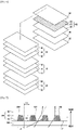
- a display device 1 includes a display module for displaying an image.
- the display module includes a display panel 100 on which an image is displayed, and a backlight unit (BLU) 20 provided to supply light to the display panel 100.
- BLU backlight unit
- the BLU 20 may include a printed circuit board 30, a light source module 40, a light guide plate 90, and an optical sheet 50.
- the light source module 40 may be arranged in the back of the display panel 100.
- the light guide plate 90 serves to transmit light emitted from the light source module 40 to the display panel 100.
- the light guide plate 90 may be arranged in the back of the display panel 100 to face the light source module 40.
- the optical sheet 50 may be arranged between the display panel 100 and the light guide plate 90 to change the optical property of the light emitted from the light source module 40.
- the display device 1 may further include a middle mold 60 to support the display panel 100, and a display chassis 70 to form the exterior of the display device 1.
- the display chassis 70 may include a top chassis 72 coupled to the front of the middle mold 60 to keep the display panel 100 in the state of being installed in the middle mold 60, and a bottom chassis 76 coupled to the back of the middle mold 60 and having the light source module 40 mounted thereon.
- the light source module 40 may be arranged on the front of the bottom chassis to be able to irradiate light to the display panel 100.
- the light source module 40 may include, for example, point light sources for emitting monochromatic light or white light.
- the display panel 100 and the top chassis 72 may be installed one after another in front of the middle mold 60, and the bottom chassis 76 may be installed behind the middle mold 60.
- the middle mold 60 not only supports the display panel 100, top chassis 72, and bottom chassis 76, but also maintains a distance between the display panel 100 and the bottom chassis 76.
- the top chassis 72 may include a bezel part 73 covering the front edge of the display panel 100, and a top side 74 bending backward from an end of the bezel part 73 and covering the side of the middle mold 60.
- the bottom chassis 76 may include a rear part 77 forming the rear side of the display device 1, and a bottom side 78 extending forward from around the rear part 77 to be coupled into the middle mold 60.
- the bottom chassis 76 may have the form of a polygonal plate with higher solidity, and may include, for example, a metal substance e.g., aluminum, aluminum alloy, etc. having less thermal deformation from the heat generated by at least one of the light source module 40 installed and the display panel 100.
- the bottom chassis 76 may be molded from, for example, plastics e.g., polycarbonate (PC) or from plastics with glass fiber added thereto.
- PC polycarbonate
- the printed circuit board 30 may be arranged on the bottom chassis 76.
- a plurality of light source modules 40 may be mounted on the printed circuit board 30.
- the size of the printed circuit board 30 may correspond to the size of the display panel 100.
- the plurality of light source modules 40 may be arranged in multiple arrays on the printed circuit board 30.
- the plurality of light source modules 40 may be arranged in a planar array on the printed circuit board 30. The light source module 40 will be described later.
- the BLU 20 may further include a reflecting sheet 80.
- the reflecting sheet 80 reflects some of the light emitted from the light source module 40, which reflects or bounces off the optical sheet 50 or the display panel 100, back to the display panel 100.
- the reflecting sheet 80 may be arranged in front of the printed circuit board 30 to reflect light leakage toward the display panel 100, thereby enhancing light efficiency.
- the reflecting sheet 80 may be located between the light guide plate 90 and the bottom chassis 76.
- the reflecting sheet 80 may be coated with higher reflective white or silver-colored coating agents, e.g., silver, TiO 2 .
- the reflecting sheet 80 may include a reflecting plate.
- the optical sheet 50 may allow the light emitted from the light source module 40 toward the display panel 100 to have higher uniformity in brightness.
- the light with a more uniform brightness, which has passed the optical sheet 50, is incident on the display panel 100.
- the optical sheet 50 may include at least one of a protective sheet, a prism sheet, or a diffusion sheet.
- the BLU 20 may include one or more optical sheets 50.
- the display device 1 as described above is a flat display device as an example, the display device 1 may include not only the flat display device but also a curved display device with a curved surface, a bendable display device with variable screen curvature, and any other display device with various forms.
- the display device 1 may include not only the edge-type display device but a direct-type display device.
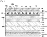
- FIG. 3 is a cross-sectional view of a display panel of a display device according to an embodiment
- FIG. 4 is an exploded perspective view of a display panel of a display device according to an embodiment.
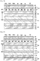
- FIGS. 5 to 11 show a display device having different display panels, each having a different array of a light absorbing material according to an embodiment.
- the display unit 100 displays an image by converting an electric signal to an optical signal.
- the display panel 100 includes a liquid crystal panel 110, and a plurality of polarizing plates 120 and 130.
- the liquid crystal panel 110 is arranged in front of the BLU 20 for blocking or transmitting the light emitted from the BLU 20.
- the front surface of the liquid crystal panel 110 forms the screen of the display device 1.
- the liquid crystal panel 110 is made up of a plurality of pixels. Each of the plurality of pixels included in the liquid crystal panel 110 may separately block or transmit the light from the BLU 20. The light transmitted through the plurality of pixels forms an image displayed on the display device 1.
- the liquid crystal panel 110 includes a first transparent substrate 111, a second transparent substrate 112, and a liquid crystal layer 114.
- the liquid crystal panel 110 further includes pixel electrodes, thin film transistors (TFTs), a common electrode, and color filters.
- the first and second transparent substrates 111 and 112 form the exterior of the liquid crystal panel 110, and protect the liquid crystal layer 114 and color filter arranged between the first and second transparent substrates 111 and 112.
- the first and second transparent substrates 111 and 112 may be made of tempered glass or transparent resin.
- the liquid crystal is in an intermediate state between solid (crystal) and fluid.
- the materials When heat is applied to ordinary materials, the materials are phase-changed from a solid state to a transparent liquid state at a temperature above their melting points.
- heat when heat is applied to a liquid crystal substance in a solid state, the liquid crystal substance changes to an opaque and muddy liquid and then into a transparent liquid state.
- Most liquid crystal materials are organic compounds, the molecules of which are shaped like thin and long rods, and the arrangement of the molecules are irregular in a direction and regular in another direction. As a result, the liquid crystal has both fluidity of a liquid and optical anisotropy of a crystal (solid).
- the liquid crystal reveals an optical property according to a change in electric field.
- the direction in which the molecules of the liquid crystal are arranged is changed according to a change in electric field.
- the liquid crystal molecules of the liquid crystal layer 114 are arranged along the direction of the electric field, and when no electric field is produced in the liquid crystal layer 114, the liquid crystal molecules may be arranged irregularly or arranged along the alignment layer.
- the optical property of the liquid crystal layer 114 may be changed according to whether there is an electric field produced to the liquid crystal layer 114. For example, if no electric field is produced in the liquid crystal layer 114, the light polarized by the first polarizing plate 120 may penetrate the liquid crystal layer 114 and then the second polarizing plate 130 due to the arrangement of the liquid crystal molecules of the liquid crystal layer 114. When an electric field is produced in the liquid crystal layer 114, the light polarized by the first polarizing plate 120 may not penetrate the second polarizing plate 130 due to being blocked by the changed arrangement of the liquid crystal molecules of the liquid crystal layer 114.
- the plurality of polarizing plates 120 and 130 are arranged on the first and second transparent substrates 111 and 112 of the liquid crystal layer 114.
- the plurality of polarizing plates 120 and 130 include the first polarizing plate 120 arranged on the rear side of the first transparent substrate 111, and the second polarizing plate 130 arranged on the front side of the second transparent substrate 112.
- the first polarizing plate 120 is arranged on a first surface 110a of the liquid crystal panel 110.
- the first polarizing plate 120 is arranged to be in contact with the first surface 110a of the liquid crystal panel 110.
- the first polarizing plate 120 may include a first protective film 122 and a first polarizing film 124.
- the first protective film 122 may be formed of a durable and non-optical material.
- the first protective film 122 may include at least one of tri-acetyl cellulose (TAC), polyethylene terephthalate (PET), and acrylic films, but are not limited thereto.
- the first polarizing film 124 may be in contact with the first protective film 122. In the embodiment, the first polarizing film 124 may be located between a pair of the first protective films 122.
- the first polarizing film 124 may include poly vynyl alcohol (PVA).
- PVA poly vynyl alcohol
- the first polarizing film 124 may include a dichromatic material in the PVA, which polarizes light to a particular direction.
- the second polarizing plate 130 is arranged on a second surface 110b of the liquid crystal panel 110. That is, the second polarizing plate 130 is arranged to be in contact with the second surface 110b of the liquid crystal panel 110.
- the second surface 110b is opposite to and corresponds to the first surface 110a.
- the first surface 110a of the liquid crystal panel 110 is directed toward the back of the display panel 100 while the second surface 110b of the liquid crystal panel 110 is directed toward the front of the display panel 100.
- the second polarizing plate 130 may include a second protective film 132 and a second polarizing film 134. There may be a pair of the second protective films 132 to protect the front and rear surfaces of the second polarizing film 134.
- the second protective film 132 may be formed of a durable and non-optical material.
- the second protective film 132 may include at least one of TAC, PET, and acrylic films.
- the second polarizing film 134 may be in contact with the second protective film 132. In the embodiment, the second polarizing film 134 may be located between the pair of the second protective films 132.
- the second polarizing film 134 may include PVA.
- the second polarizing film 134 may include a dichromatic material in the PVA, which polarizes light to a particular direction.
- Light has a pair of electric field and magnetic field oscillating in different directions perpendicular to a traveling direction of light.
- the directions of oscillation of the electric and magnetic fields may be any different directions perpendicular to the traveling direction of light.
- the phenomenon that an electric field or a magnetic field oscillates in only a particular direction is called polarization, and a polarizer film may transmit light having an electric or magnetic field oscillating in a predetermined direction while blocking light having an electric or magnetic field oscillating in a direction other than the predetermined direction.
- the polarizing film transmits light oscillating in a predetermined direction but blocks light oscillating in the other directions.
- the first polarizing film 124 may transmit light having an electric or magnetic field oscillating in a first direction while blocking other light.
- the second polarizing film 134 may transmit light having an electric or magnetic field oscillating in a second direction while blocking other light.
- the first and second directions may be perpendicular to each other. In other words, the direction in which the light transmitted through the first polarizing film 124 oscillates and the direction in which the light transmitted through the second polarizing film 134 oscillates may be perpendicular to each other. As a result, the light in general may not penetrate both the first and second polarizing films 124 and 134 at the same time.
- the display panel 100 further includes a light absorbing layer 140.
- the light absorbing layer 140 is arranged to receive the light having passed the liquid crystal panel 110 and the plurality of polarizing plates 120 and 130.
- the light emitted from the light source module 40 passes the first polarizing plate 120, the liquid crystal panel 110, and the second polarizing plate 130, successively.
- Light passing the second polarizing plate 130 is incident on the light absorbing layer 140.
- the light absorbing layer 140 is arranged on the second polarizing plate 130 to absorb a portion of the light supplied from the BLU 20.
- the light supplied from the light source module 40 may be diffused due to the difference in refractive index between the internal components of the display panel 100. This phenomenon may result in light leakage from the display panel 100, which interferes with expression of a desired color at a certain angle from the front of the display device 1.
- Light absorbers 170 enhance the image quality of the display device 1 by absorbing the unnecessarily emitted light or reflecting it toward the front of the display device 1.
- the light absorbing layer 140 includes a first resin layer 150, a second resin layer 160, and the light absorbers 170.
- the first and second resin layers 150 and 160 include transparent resin capable of transmitting light.
- the first and second resin layers 150 and 160 may be formed to be as wide as the width of the second polarizing plate 130.
- the first resin layer 150 is arranged on the back surface of the second resin layer 160.
- the first and second resin layers 150 and 160 may have corresponding width to each other.
- the first resin layer 150 has a refractive index lower than that of the second resin layer 160. Since the first and second resin layers 150 and 160 have optical surfaces parallel to the liquid crystal panel 110, the light may be inclined with respect to the front-back direction toward the front while traveling from the first resin layer 150 to the second resin layer 160. That is, the light may be directed to the front of the display device 1 while passing the first and second resin layers 150 and 160.
- the difference in refractive index n1 and n2 between the first and second resin layers 150 and 160 may bc, for example, 0.1 or more.
- the first resin layer 150 includes a first optical surface 152 directed to the second polarizing plate 130, and a second optical surface 154, on the opposite side of the first optical surface 152, coming into contact with the second resin layer 160.
- the first resin layer 150 includes a plurality of grooves 156 concavely formed on the first optical surface 152.
- the cross-section of the plurality of grooves 156 may have the form of trapezoids. However, embodiments are not limited thereto, and the cross-section of the plurality of grooves 156 may also have the form of triangles, rectangles, partial circles, half circles, ovals, or any combination thereof.
- the light absorbers 170 absorb a portion of the light passing the light absorbing layer 140.
- the light absorbers 170 are provided in the first resin layer 150. Specifically, the light absorbers 170 are arranged in the plurality grooves 156 formed on the first optical surface 152 of the first resin layer 150.
- the light absorbers 170 may be formed to fill the concave space of the plurality of grooves 156.
- the light absorbers 170 may be arranged to fill at least a part of each groove 156. For example, the light absorbers 170 fully or partially fill each groove 156 according to the shape, size, purpose, etc., of the display device 1.
- the light incident on the light absorbing layer 140 some light inclined at more than a certain angle from a baseline extending in the front-back direction of the display panel 100 is absorbed by the light absorbing layer 140.
- some light inclined at more than a certain angle from a baseline extending in the front-back direction of the display panel 100 is absorbed by the light absorbers 170.
- the plurality of grooves 156 are formed on the second optical surface 154 of the first resin layer 150, and the light absorbers 170 are arranged in the plurality of grooves 156 formed on the second optical surface 154.
- the light absorbers 170 are arranged in the first resin layer 150 while not exposed through the first and second optical surfaces 152 and 154 and, the light absorbers 170 are arranged in the first resin layer 150 to absorb a portion of the light passing the light absorbing layer 140.
- the plurality of grooves 156 may be formed to have a cross-section with the length in the front-back direction being longer than the width in the left-right direction. This structure may more efficiently absorb a portion of the light incident on the light absorbing layer 140, which is inclined at more than a certain angle from the front-back direction of the display device 1. Consequently, the light incident on the light absorbing layer 140 may be mostly directed to the front of the display device 1.
- the light absorbers 170 arranged in the plurality of grooves 156 may be elongated in one direction in the first resin layer 150 and may be arrayed in another direction perpendicular to the one direction, as shown in FIG. 4 .
- the light absorbers 170 are elongated in the longitudinal direction of the first resin layer 150 and arrayed in the lateral direction of the first resin layer 150.
- the light absorbers 170 may be elongated in the vertical direction of the first resin layer 150 and arrayed in the horizontal direction of the first resin layer 150.
- the light absorbers 170 may be arrayed regularly in the first resin layer 150. This may reduce or prevent the light inclined at more than a certain angle from a baseline extending in the front-back direction of the display panel 100 toward the left-right (or horizontal) direction of the display panel 100 from being emitted in the horizontal direction of the display panel 100.
- the plurality of grooves 156 may be elongated in one direction on the first resin layer 150 and may be arrayed in another direction perpendicular to the one direction.
- the plurality of grooves 156 may be elongated in the longitudinal direction of the first resin layer 150 and arrayed in the lateral direction of the first resin layer 150. That is, the plurality of grooves 156 may be elongated in the vertical direction of the first resin layer 150 and arrayed in the horizontal direction of the first resin layer 150.
- the plurality of grooves 156 may be arranged regularly on the first resin layer 150.
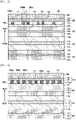
- the plurality of grooves 156 may include a first groove 156aa, a second groove 156bb separated by first length L1 from the first groove 156aa, and a third groove 156cc separated by second length L2 from the second groove 156bb.
- the first length L1 may be the same as the second length L2
- the plurality of grooves 156 may be arranged at regular intervals on the first resin layer 150.
- the light passing the liquid crystal panel 110 is absorbed or reflected while passing the liquid crystal panel 110, a portion of the light inclined at less than a certain angle from a baseline extending in the front-back direction of the display panel 100 may be emitted. Subsequently, the light emitted from the first resin layer 150 may be further refracted toward the front while being incident on the second resin layer 160.
- the light absorbers 170 may include, for example, at least one of carbon black, black resin, a compound of metal particles, graphite power, gravure ink, black spray, and black enamel.
- the shape of the cross-section of the optical absorbers 170 may correspond to the cross-sectional feature of the plurality of grooves 156.
- the cross-sectional features of the light absorbers 170 and the plurality of grooves 156 may have the form of trapezoids whose width becomes smaller along the depth.
- the width and the height of the cross-section of each of the light absorbers 170 are La and Lb, and the gap between the neighboring light absorbers 170 are Lc, they may be defined as follows:
- La, Lb, and Lc are defined when the cross-section of each light absorber 170 has the form of a trapezoid in the embodiment, the light absorbers 170 may have any other forms as long as the above relations are met.
- La, Lb, and Lc may also refer to the width and the height of the cross-section of each of the plurality of grooves 156 and the gap between the neighboring grooves 156.
- the display panel 100 may further include an adhesive layer 180.
- the adhesive layer 180 may be arranged between the light absorbing layer 140 and the second polarizing plate 130.
- the adhesive layer 180 may be provided for the light absorbing layer 140 to be adhered to the second polarizing plate 130. That is, the adhesive layer 180 may be arranged between the light absorbing layer 140 and the second polarizing plate 130 such that the light absorbing layer 140 and the second polarizing plate 130 are bonded together.
- the adhesive layer 180 may have a refractive index, which is the same as or less than the refractive index of the first resin layer 150.
- the adhesive layer 180 may have a refractive index, which is the same as or less than the refractive index of the first resin layer 150, to reduce or prevent the adhesive layer 180 from causing the light emitted from the second polarizing plate 130 to have a large angle of emission.
- the display panel 100 may further include the protective film 190 applied on the front surface of the light absorbing layer 140.
- the protective film 190 may be provided to come into contact with the outer surface of the second resin layer 160 of the light absorbing layer 140.
- the protective film 190 may include at least one of TAC, PET, and acrylic films.
- the display panel 100 may include a surface layer 192 applied onto the front surface of the protective film 190. In other words, the surface layer 192 may be arranged on the outer surface of the protective film 190.
- the light absorbing layer 140 may be manufactured in a module and adhered to the second polarizing plate 130.
- the first polarizing plate 120, the second polarizing plate 130, the liquid crystal panel 110, and the light absorbing layer 140 may be separately manufactured and then combined together.
- the first resin layer 150 may be layered on the second resin layer 160.
- a plurality of grooves 156 may then be formed on the first resin layer 150, and the light absorbers 170 may be injected or inserted to the plurality of grooves 156.
- the light absorbing layer 140 manufactured in this way may be adhered to a surface of the second polarizing plate 130 through the adhesive layer 180.
- the protective film 190 or the surface layer 192 arranged in front of the light absorbing layer 140 may be layered on the light absorbing layer 140 after the light absorbing layer 140 is adhered to the second polarizing plate 130.
- the method of manufacturing the light absorbing layer 140 is not, however, limited thereto, and may vary.
- the light absorbing layer 140 may be manufactured in a module such that the second resin layer 160 is arranged at the bottom of the light absorbing layer 140.
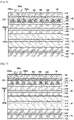
- the display panel 100 further includes a light absorbing material 200 contained in the light absorbing layer 140 to absorb light of particular wavelengths.
- the light absorbing material 200 is contained in at least one from among the first resin layer 150, the second resin layer 160, and the light absorbers 170.
- FIG. 5 shows an example that the light absorbing material 200 is contained in the light absorbers 170.
- FIG. 5 shows a case where the light absorbing material 200 is included in the plurality of grooves 156 along with the light absorbers 170.
- FIG. 6 shows an example that the light absorbing material 200 is contained in the first resin layer 150
- FIG. 7 shows an example that the light absorbing material 200 is contained in the second resin layer 160.
- FIG. 8 shows an example that the light absorbing material 200 is contained in the light absorbers 170 and the first resin layer 150
- FIG. 9 shows an example that the light absorbing material 200 is contained in the light absorbers 170 and the second resin layer 160
- FIG. 10 shows an example that the light absorbing material 200 is contained in the first and second resin layers 150 and 160
- FIG. 11 shows an example that the light absorbing material 200 is contained in the first and second resin layers 150 and 160 and the light absorbers 170.
- the light absorbing material 200 absorbs light of predetermined wavelengths and may comprise at least one pigment configured to absorb the light of the predetermined wavelengths.
- the light absorbers 170 absorb or reflect the unnecessarily emitted light toward the front of the display panel 100, thereby enhancing the image quality of the display device 1.
- the light absorbing material 200 further enhances the image quality of the display device 1 by supplementing the role of the light absorbers 170.
- the light absorbing material 200 is applied to reduce or prevent occurrence of mura like a stain on the screen of the display device 1.
- the light absorbing material 200 helps to enhance color reproducibility and uniformity of brightness of the display device 1 by absorbing the unnecessarily emitted light of particular wavelengths.
- FIG. 12 is a cross-sectional view of a display panel of a display device, according to an embodiment of the present invention.
- reference numeral 200 represents the light absorbing material.
- the plurality of grooves 156 may include the first groove 156aa, the second groove 156bb separated by the first length L1 from the first groove 156aa, and the third groove 156cc separated by the second length L2 from the second groove 156bb.
- the first length L1 may be different from the second length L2.
- the gap between the neighboring grooves 156 may vary depending on the arrangement of the light source module 40, internal configurations of the optical sheet 50 or the display panel 100.
- FIGS. 13 to 17 are cross-sectional views of a display panel of a display device according to an embodiment.
- reference numeral 200 represents the light absorbing material.
- the first resin layer 150 includes a plurality of grooves 156a concavely formed thereon.
- the plurality of grooves 156a may have the form of squares. Accordingly, light absorbers 170a filling the concave space formed in the plurality of grooves 156a may also have the form of squares.
- a plurality of grooves 156b may have the form of triangles. Accordingly, light absorbers 170b filling the concave space formed in the plurality of grooves 156b may also have the form of triangles.
- a plurality of grooves 156c may have the form of semicircles. Accordingly, light absorbers 170c filling the concave space formed in the plurality of grooves 156c may also have the form of semicircles.
- a plurality of grooves 156d may have the form of full or partial ellipses. Accordingly, light absorbers 170d filling the concave space formed in the plurality of grooves 156d may also have the form of full or partial ellipses.
- a plurality of grooves 156e may have the combined form of the aforementioned figures.
- the plurality of grooves 156e may have the combined form of triangle and square.
- light absorbers 170e filling the concave space formed in the plurality of grooves 156e may also have the combined form of triangle and square.
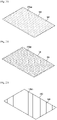
- FIGS. 18 to 23 are perspective views of a first resin layer of a display device according to an embodiment.
- a plurality of grooves filled with light absorbers 170aa is arrayed on the first resin layer 150.
- the light absorbers 170aa filling the plurality of grooves are elongated in the horizontal direction of the display panel 100 and arrayed in the vertical direction.
- the light absorbers 170aa may be arrayed regularly in the first resin layer 150. This may reduce or prevent the light inclined at more than a certain angle from a baseline extending in the front-back direction of the display panel 100 toward the vertical direction of the display panel 100 from being emitted in the vertical direction of the display panel 100.
- a plurality of light absorbers 170bb filling a plurality of grooves are elongated to cross each other in the horizontal and vertical directions of the display panel 100, and arrayed in the vertical and horizontal directions.
- the light absorbers 170bb are arrayed in the first resin layer 150.
- the light absorbers 170bb may be arrayed regularly in the first resin layer 150. This may reduce or prevent the light from being emitted while being inclined at more than a certain angle from the vertical and horizontal directions.
- a plurality of light absorbers 170cc filling a plurality of grooves are elongated in the diagonal direction of the display panel 100, and arrayed in a direction perpendicular to the diagonal direction.
- the light absorbers 170cc are arrayed in the first resin layer 150.
- the light absorbers 170cc may be arrayed regularly in the first resin layer 150. This may reduce or prevent the light from being emitted while being inclined at more than a certain angle from the front of the display panel 100 toward the direction perpendicular to the diagonal direction.
- light absorbers 170dd filling a plurality of grooves may have the form of dots and distributed in the first resin layer 150.
- the light absorbers 170dd may be distributed uniformly as shown in FIG. 21 , or may be more densely distributed in a certain area.
- a plurality of light absorbers 170ee filling a plurality of grooves may have the form of waves traveling in one direction, and arrayed in a direction perpendicular to the one direction.
- the light absorbers 170ee may be arrayed regularly in the first resin layer 150. This may reduce or prevent the light from being emitted while being inclined at more than a certain angle from the vertical and horizontal directions of the display panel 100.
- a plurality of light absorbers 170ff filling a plurality of grooves may be arrayed in the first resin layer 150 with different densities of intervals depending on the areas.
- the light absorbers 170ff may include first light absorbers 177ff1 arrayed in first areas and second light absorbers 177ff2 arrayed in second areas.
- the first light absorbers 177ff1 may be arrayed more densely than the second light absorbers 177ff2. While the first areas are on the left and right sides in the embodiment, they are not limited thereto.
- the light absorbing material 200 may be applied to the display panel of as shown in FIG. 3 .
- embodiments are not limited thereto, and the light absorbing material 200 may be applied to the display panels of FIGS. 12 to 17 .
Description
- The invention relates to a display device, and more particularly, to a display device with enhanced uniformity of brightness.
- Display devices are a kind of output device for visually providing data information such as characters, figures, etc., and still or video images.
- The display device may include an active light-emitting display panel such as organic light emitting diodes (OLEDs) or a passive light-emitting display panel such as liquid crystal displays (LCDs). Examples of liquid crystal displays are disclosed in
JP 2015 052796 JP 2017 167506 - A display device employing the passive light-emitting display panel may include a backlight unit for supplying light to the display panel.
- The display device with the passive light-emitting display panel has difficulty in realizing a pure black screen, because some light leaks out of the light source of the backlight unit that is always turned on.
- Provided is a display device with an enhanced structure to facilitate realization of black screens.
- Provided is a display device with an enhanced structure to prevent mura.
- Provided is a display device having high color reproducibility.
- A display device according to the invention is defined in
claim 1 while further embodiments of the invention are defined in the dependent claims. - According to the invention , a display device may be obtained, which may reduce or prevent mura that looks like a stain, by adding a light absorbing material that absorbs light in a particular wavelength range to a light absorbing layer, thereby enhancing uniformity of brightness and color reproducibility and facilitating realization of black screens.
-
-
FIG. 1 is a perspective view of a display device according to an embodiment; -
FIG. 2 is a cross-sectional view of a display device according to an embodiment; -
FIG. 3 is a cross-sectional view of a display panel of a display device according to an embodiment; -
FIG. 4 is an exploded perspective view of a display panel of a display device according to an embodiment; -
FIGS. 5 to 11 show a display device having different display panels, each having a different array of a light absorbing material, according to an embodiment; -
FIG. 12 is a cross-sectional view of a display panel of a display device according to an embodiment; -
FIGS. 13 to 17 are cross-sectional views of a display panel of a display device according to an embodiment; and -
FIGS. 18 to 23 are perspective views of a first resin layer of a display device according to an embodiment. - Reference will now be made in detail to embodiments of the invention as claimed, examples of which are illustrated in the accompanying drawings, wherein like reference numerals refer to the like elements throughout. The terms "front", "rear", "upper", "lower", "top", and "bottom" as herein used are defined based on the drawings, but the terms may not restrict the shape and position of the respective components.
-
FIG. 1 is a perspective view of a display device according to an embodiment, andFIG. 2 is a cross-sectional view of a display device according to an embodiment. - A
display device 1 includes a display module for displaying an image. - The display module includes a
display panel 100 on which an image is displayed, and a backlight unit (BLU) 20 provided to supply light to thedisplay panel 100. - The BLU 20 may include a printed
circuit board 30, alight source module 40, alight guide plate 90, and anoptical sheet 50. Thelight source module 40 may be arranged in the back of thedisplay panel 100. Thelight guide plate 90 serves to transmit light emitted from thelight source module 40 to thedisplay panel 100. Thelight guide plate 90 may be arranged in the back of thedisplay panel 100 to face thelight source module 40. Theoptical sheet 50 may be arranged between thedisplay panel 100 and thelight guide plate 90 to change the optical property of the light emitted from thelight source module 40. - The
display device 1 may further include amiddle mold 60 to support thedisplay panel 100, and adisplay chassis 70 to form the exterior of thedisplay device 1. Thedisplay chassis 70 may include atop chassis 72 coupled to the front of themiddle mold 60 to keep thedisplay panel 100 in the state of being installed in themiddle mold 60, and abottom chassis 76 coupled to the back of themiddle mold 60 and having thelight source module 40 mounted thereon. - The
light source module 40 may be arranged on the front of the bottom chassis to be able to irradiate light to thedisplay panel 100. Thelight source module 40 may include, for example, point light sources for emitting monochromatic light or white light. - The
display panel 100 and thetop chassis 72 may be installed one after another in front of themiddle mold 60, and thebottom chassis 76 may be installed behind themiddle mold 60. Themiddle mold 60 not only supports thedisplay panel 100,top chassis 72, andbottom chassis 76, but also maintains a distance between thedisplay panel 100 and thebottom chassis 76. - The
top chassis 72 may include abezel part 73 covering the front edge of thedisplay panel 100, and atop side 74 bending backward from an end of thebezel part 73 and covering the side of themiddle mold 60. - The
bottom chassis 76 may include arear part 77 forming the rear side of thedisplay device 1, and a bottom side 78 extending forward from around therear part 77 to be coupled into themiddle mold 60. Thebottom chassis 76 may have the form of a polygonal plate with higher solidity, and may include, for example, a metal substance e.g., aluminum, aluminum alloy, etc. having less thermal deformation from the heat generated by at least one of thelight source module 40 installed and thedisplay panel 100. Thebottom chassis 76 may be molded from, for example, plastics e.g., polycarbonate (PC) or from plastics with glass fiber added thereto. - The printed
circuit board 30 may be arranged on thebottom chassis 76. A plurality oflight source modules 40 may be mounted on the printedcircuit board 30. The size of the printedcircuit board 30 may correspond to the size of thedisplay panel 100. The plurality oflight source modules 40 may be arranged in multiple arrays on the printedcircuit board 30. The plurality oflight source modules 40 may be arranged in a planar array on the printedcircuit board 30. Thelight source module 40 will be described later. - The BLU 20 may further include a reflecting
sheet 80. The reflectingsheet 80 reflects some of the light emitted from thelight source module 40, which reflects or bounces off theoptical sheet 50 or thedisplay panel 100, back to thedisplay panel 100. The reflectingsheet 80 may be arranged in front of the printedcircuit board 30 to reflect light leakage toward thedisplay panel 100, thereby enhancing light efficiency. The reflectingsheet 80 may be located between thelight guide plate 90 and thebottom chassis 76. The reflectingsheet 80 may be coated with higher reflective white or silver-colored coating agents, e.g., silver, TiO2. The reflectingsheet 80 may include a reflecting plate. - The
optical sheet 50 may allow the light emitted from thelight source module 40 toward thedisplay panel 100 to have higher uniformity in brightness. The light with a more uniform brightness, which has passed theoptical sheet 50, is incident on thedisplay panel 100. Theoptical sheet 50 may include at least one of a protective sheet, a prism sheet, or a diffusion sheet. The BLU 20 may include one or moreoptical sheets 50. - While the
display device 1 as described above is a flat display device as an example, thedisplay device 1 may include not only the flat display device but also a curved display device with a curved surface, a bendable display device with variable screen curvature, and any other display device with various forms. - Furthermore, while an edge-type display device has been focused and described above, the
display device 1 may include not only the edge-type display device but a direct-type display device. -
FIG. 3 is a cross-sectional view of a display panel of a display device according to an embodiment, andFIG. 4 is an exploded perspective view of a display panel of a display device according to an embodiment.FIGS. 5 to 11 show a display device having different display panels, each having a different array of a light absorbing material according to an embodiment. - As shown in
FIGS. 3 to 11 , thedisplay unit 100 displays an image by converting an electric signal to an optical signal. Thedisplay panel 100 includes aliquid crystal panel 110, and a plurality ofpolarizing plates - The
liquid crystal panel 110 is arranged in front of theBLU 20 for blocking or transmitting the light emitted from theBLU 20. - The front surface of the
liquid crystal panel 110 forms the screen of thedisplay device 1. Theliquid crystal panel 110 is made up of a plurality of pixels. Each of the plurality of pixels included in theliquid crystal panel 110 may separately block or transmit the light from theBLU 20. The light transmitted through the plurality of pixels forms an image displayed on thedisplay device 1. - The
liquid crystal panel 110 includes a firsttransparent substrate 111, a secondtransparent substrate 112, and aliquid crystal layer 114. Theliquid crystal panel 110 further includes pixel electrodes, thin film transistors (TFTs), a common electrode, and color filters. The first and secondtransparent substrates liquid crystal panel 110, and protect theliquid crystal layer 114 and color filter arranged between the first and secondtransparent substrates transparent substrates - The liquid crystal is in an intermediate state between solid (crystal) and fluid. When heat is applied to ordinary materials, the materials are phase-changed from a solid state to a transparent liquid state at a temperature above their melting points. By contrast, when heat is applied to a liquid crystal substance in a solid state, the liquid crystal substance changes to an opaque and muddy liquid and then into a transparent liquid state. Most liquid crystal materials are organic compounds, the molecules of which are shaped like thin and long rods, and the arrangement of the molecules are irregular in a direction and regular in another direction. As a result, the liquid crystal has both fluidity of a liquid and optical anisotropy of a crystal (solid).
- Furthermore, the liquid crystal reveals an optical property according to a change in electric field. For example, the direction in which the molecules of the liquid crystal are arranged is changed according to a change in electric field.
- When an electric field is produced in the
liquid crystal layer 114, the liquid crystal molecules of theliquid crystal layer 114 are arranged along the direction of the electric field, and when no electric field is produced in theliquid crystal layer 114, the liquid crystal molecules may be arranged irregularly or arranged along the alignment layer. - Consequently, the optical property of the
liquid crystal layer 114 may be changed according to whether there is an electric field produced to theliquid crystal layer 114. For example, if no electric field is produced in theliquid crystal layer 114, the light polarized by the firstpolarizing plate 120 may penetrate theliquid crystal layer 114 and then the secondpolarizing plate 130 due to the arrangement of the liquid crystal molecules of theliquid crystal layer 114. When an electric field is produced in theliquid crystal layer 114, the light polarized by the firstpolarizing plate 120 may not penetrate the secondpolarizing plate 130 due to being blocked by the changed arrangement of the liquid crystal molecules of theliquid crystal layer 114. - The plurality of
polarizing plates transparent substrates liquid crystal layer 114. - The plurality of
polarizing plates polarizing plate 120 arranged on the rear side of the firsttransparent substrate 111, and the secondpolarizing plate 130 arranged on the front side of the secondtransparent substrate 112. - The first
polarizing plate 120 is arranged on afirst surface 110a of theliquid crystal panel 110. For example, the firstpolarizing plate 120 is arranged to be in contact with thefirst surface 110a of theliquid crystal panel 110. The firstpolarizing plate 120 may include a firstprotective film 122 and a firstpolarizing film 124. The firstprotective film 122 may be formed of a durable and non-optical material. For example, the firstprotective film 122 may include at least one of tri-acetyl cellulose (TAC), polyethylene terephthalate (PET), and acrylic films, but are not limited thereto. - The first
polarizing film 124 may be in contact with the firstprotective film 122. In the embodiment, the firstpolarizing film 124 may be located between a pair of the firstprotective films 122. The firstpolarizing film 124 may include poly vynyl alcohol (PVA). The firstpolarizing film 124 may include a dichromatic material in the PVA, which polarizes light to a particular direction. - The second
polarizing plate 130 is arranged on asecond surface 110b of theliquid crystal panel 110. That is, the secondpolarizing plate 130 is arranged to be in contact with thesecond surface 110b of theliquid crystal panel 110. Thesecond surface 110b is opposite to and corresponds to thefirst surface 110a. For example, thefirst surface 110a of theliquid crystal panel 110 is directed toward the back of thedisplay panel 100 while thesecond surface 110b of theliquid crystal panel 110 is directed toward the front of thedisplay panel 100. The secondpolarizing plate 130 may include a secondprotective film 132 and a secondpolarizing film 134. There may be a pair of the secondprotective films 132 to protect the front and rear surfaces of the secondpolarizing film 134. The secondprotective film 132 may be formed of a durable and non-optical material. For example, the secondprotective film 132 may include at least one of TAC, PET, and acrylic films. - The second
polarizing film 134 may be in contact with the secondprotective film 132. In the embodiment, the secondpolarizing film 134 may be located between the pair of the secondprotective films 132. The secondpolarizing film 134 may include PVA. The secondpolarizing film 134 may include a dichromatic material in the PVA, which polarizes light to a particular direction. - Light has a pair of electric field and magnetic field oscillating in different directions perpendicular to a traveling direction of light. The directions of oscillation of the electric and magnetic fields may be any different directions perpendicular to the traveling direction of light. The phenomenon that an electric field or a magnetic field oscillates in only a particular direction is called polarization, and a polarizer film may transmit light having an electric or magnetic field oscillating in a predetermined direction while blocking light having an electric or magnetic field oscillating in a direction other than the predetermined direction. The polarizing film transmits light oscillating in a predetermined direction but blocks light oscillating in the other directions.
- The first
polarizing film 124 may transmit light having an electric or magnetic field oscillating in a first direction while blocking other light. The secondpolarizing film 134 may transmit light having an electric or magnetic field oscillating in a second direction while blocking other light. The first and second directions may be perpendicular to each other. In other words, the direction in which the light transmitted through the firstpolarizing film 124 oscillates and the direction in which the light transmitted through the secondpolarizing film 134 oscillates may be perpendicular to each other. As a result, the light in general may not penetrate both the first and secondpolarizing films - The
display panel 100 further includes a lightabsorbing layer 140. The lightabsorbing layer 140 is arranged to receive the light having passed theliquid crystal panel 110 and the plurality ofpolarizing plates light source module 40 passes the firstpolarizing plate 120, theliquid crystal panel 110, and the secondpolarizing plate 130, successively. Light passing the secondpolarizing plate 130 is incident on thelight absorbing layer 140. The lightabsorbing layer 140 is arranged on the secondpolarizing plate 130 to absorb a portion of the light supplied from theBLU 20. - The light supplied from the
light source module 40 may be diffused due to the difference in refractive index between the internal components of thedisplay panel 100. This phenomenon may result in light leakage from thedisplay panel 100, which interferes with expression of a desired color at a certain angle from the front of thedisplay device 1.Light absorbers 170 enhance the image quality of thedisplay device 1 by absorbing the unnecessarily emitted light or reflecting it toward the front of thedisplay device 1. - The light
absorbing layer 140 includes afirst resin layer 150, asecond resin layer 160, and thelight absorbers 170. The first and second resin layers 150 and 160 include transparent resin capable of transmitting light. The first and second resin layers 150 and 160 may be formed to be as wide as the width of the secondpolarizing plate 130. - The
first resin layer 150 is arranged on the back surface of thesecond resin layer 160. The first and second resin layers 150 and 160 may have corresponding width to each other. Thefirst resin layer 150 has a refractive index lower than that of thesecond resin layer 160. Since the first and second resin layers 150 and 160 have optical surfaces parallel to theliquid crystal panel 110, the light may be inclined with respect to the front-back direction toward the front while traveling from thefirst resin layer 150 to thesecond resin layer 160. That is, the light may be directed to the front of thedisplay device 1 while passing the first and second resin layers 150 and 160. The difference in refractive index n1 and n2 between the first and second resin layers 150 and 160 may bc, for example, 0.1 or more. - The
first resin layer 150 includes a firstoptical surface 152 directed to the secondpolarizing plate 130, and a secondoptical surface 154, on the opposite side of the firstoptical surface 152, coming into contact with thesecond resin layer 160. Thefirst resin layer 150 includes a plurality ofgrooves 156 concavely formed on the firstoptical surface 152. The cross-section of the plurality ofgrooves 156 may have the form of trapezoids. However, embodiments are not limited thereto, and the cross-section of the plurality ofgrooves 156 may also have the form of triangles, rectangles, partial circles, half circles, ovals, or any combination thereof. - The
light absorbers 170 absorb a portion of the light passing thelight absorbing layer 140. Thelight absorbers 170 are provided in thefirst resin layer 150. Specifically, thelight absorbers 170 are arranged in theplurality grooves 156 formed on the firstoptical surface 152 of thefirst resin layer 150. Thelight absorbers 170 may be formed to fill the concave space of the plurality ofgrooves 156. Thelight absorbers 170 may be arranged to fill at least a part of eachgroove 156. For example, thelight absorbers 170 fully or partially fill eachgroove 156 according to the shape, size, purpose, etc., of thedisplay device 1. Of the light incident on thelight absorbing layer 140, some light inclined at more than a certain angle from a baseline extending in the front-back direction of thedisplay panel 100 is absorbed by thelight absorbing layer 140. For example, of the light incident on thelight absorbing layer 140, some light inclined at more than a certain angle from a baseline extending in the front-back direction of thedisplay panel 100 is absorbed by thelight absorbers 170. - Alternatively, but also according to the invention as claimed, the plurality of
grooves 156 are formed on the secondoptical surface 154 of thefirst resin layer 150, and thelight absorbers 170 are arranged in the plurality ofgrooves 156 formed on the secondoptical surface 154. Further alternatively, but also according to the invention as claimed, thelight absorbers 170 are arranged in thefirst resin layer 150 while not exposed through the first and secondoptical surfaces light absorbers 170 are arranged in thefirst resin layer 150 to absorb a portion of the light passing thelight absorbing layer 140. - The plurality of
grooves 156 may be formed to have a cross-section with the length in the front-back direction being longer than the width in the left-right direction. This structure may more efficiently absorb a portion of the light incident on thelight absorbing layer 140, which is inclined at more than a certain angle from the front-back direction of thedisplay device 1. Consequently, the light incident on thelight absorbing layer 140 may be mostly directed to the front of thedisplay device 1. - The
light absorbers 170 arranged in the plurality ofgrooves 156 may be elongated in one direction in thefirst resin layer 150 and may be arrayed in another direction perpendicular to the one direction, as shown inFIG. 4 . In the embodiment, thelight absorbers 170 are elongated in the longitudinal direction of thefirst resin layer 150 and arrayed in the lateral direction of thefirst resin layer 150. For example, referring toFIG. 4 , thelight absorbers 170 may be elongated in the vertical direction of thefirst resin layer 150 and arrayed in the horizontal direction of thefirst resin layer 150. In the embodiment, thelight absorbers 170 may be arrayed regularly in thefirst resin layer 150. This may reduce or prevent the light inclined at more than a certain angle from a baseline extending in the front-back direction of thedisplay panel 100 toward the left-right (or horizontal) direction of thedisplay panel 100 from being emitted in the horizontal direction of thedisplay panel 100. - To correspond to the
optical absorbers 170 arranged in thefirst resin layer 150, the plurality ofgrooves 156 may be elongated in one direction on thefirst resin layer 150 and may be arrayed in another direction perpendicular to the one direction. In the embodiment, the plurality ofgrooves 156 may be elongated in the longitudinal direction of thefirst resin layer 150 and arrayed in the lateral direction of thefirst resin layer 150. That is, the plurality ofgrooves 156 may be elongated in the vertical direction of thefirst resin layer 150 and arrayed in the horizontal direction of thefirst resin layer 150. - The plurality of
grooves 156 may be arranged regularly on thefirst resin layer 150. The plurality ofgrooves 156 may include a first groove 156aa, a second groove 156bb separated by first length L1 from the first groove 156aa, and a third groove 156cc separated by second length L2 from the second groove 156bb. In the embodiment, the first length L1 may be the same as the second length L2, and the plurality ofgrooves 156 may be arranged at regular intervals on thefirst resin layer 150. - Since the light passing the
liquid crystal panel 110 is absorbed or reflected while passing theliquid crystal panel 110, a portion of the light inclined at less than a certain angle from a baseline extending in the front-back direction of thedisplay panel 100 may be emitted. Subsequently, the light emitted from thefirst resin layer 150 may be further refracted toward the front while being incident on thesecond resin layer 160. - The
light absorbers 170 may include, for example, at least one of carbon black, black resin, a compound of metal particles, graphite power, gravure ink, black spray, and black enamel. - The shape of the cross-section of the
optical absorbers 170 may correspond to the cross-sectional feature of the plurality ofgrooves 156. The cross-sectional features of thelight absorbers 170 and the plurality ofgrooves 156 may have the form of trapezoids whose width becomes smaller along the depth. When the width and the height of the cross-section of each of thelight absorbers 170 are La and Lb, and the gap between the neighboringlight absorbers 170 are Lc, they may be defined as follows: - 5µm ≤ La ≤ 20µm
- 10µm ≤ Lb ≤ 40µm
- 15µm ≤ Lc ≤ 50µm
- While La, Lb, and Lc are defined when the cross-section of each
light absorber 170 has the form of a trapezoid in the embodiment, thelight absorbers 170 may have any other forms as long as the above relations are met. La, Lb, and Lc may also refer to the width and the height of the cross-section of each of the plurality ofgrooves 156 and the gap between the neighboringgrooves 156. - The
display panel 100 may further include anadhesive layer 180. - The
adhesive layer 180 may be arranged between the light absorbinglayer 140 and the secondpolarizing plate 130. Theadhesive layer 180 may be provided for thelight absorbing layer 140 to be adhered to the secondpolarizing plate 130. That is, theadhesive layer 180 may be arranged between the light absorbinglayer 140 and the secondpolarizing plate 130 such that thelight absorbing layer 140 and the secondpolarizing plate 130 are bonded together. Theadhesive layer 180 may have a refractive index, which is the same as or less than the refractive index of thefirst resin layer 150. In other words, theadhesive layer 180 may have a refractive index, which is the same as or less than the refractive index of thefirst resin layer 150, to reduce or prevent theadhesive layer 180 from causing the light emitted from the secondpolarizing plate 130 to have a large angle of emission. - The
display panel 100 may further include theprotective film 190 applied on the front surface of thelight absorbing layer 140. Theprotective film 190 may be provided to come into contact with the outer surface of thesecond resin layer 160 of thelight absorbing layer 140. Theprotective film 190 may include at least one of TAC, PET, and acrylic films. Thedisplay panel 100 may include asurface layer 192 applied onto the front surface of theprotective film 190. In other words, thesurface layer 192 may be arranged on the outer surface of theprotective film 190. - The light
absorbing layer 140 may be manufactured in a module and adhered to the secondpolarizing plate 130. For example, the firstpolarizing plate 120, the secondpolarizing plate 130, theliquid crystal panel 110, and thelight absorbing layer 140 may be separately manufactured and then combined together. - To manufacture the
light absorbing layer 140, thefirst resin layer 150 may be layered on thesecond resin layer 160. A plurality ofgrooves 156 may then be formed on thefirst resin layer 150, and thelight absorbers 170 may be injected or inserted to the plurality ofgrooves 156. The lightabsorbing layer 140 manufactured in this way may be adhered to a surface of the secondpolarizing plate 130 through theadhesive layer 180. - The
protective film 190 or thesurface layer 192 arranged in front of thelight absorbing layer 140 may be layered on thelight absorbing layer 140 after thelight absorbing layer 140 is adhered to the secondpolarizing plate 130. The method of manufacturing thelight absorbing layer 140 is not, however, limited thereto, and may vary. For example, thelight absorbing layer 140 may be manufactured in a module such that thesecond resin layer 160 is arranged at the bottom of thelight absorbing layer 140. - The
display panel 100 further includes alight absorbing material 200 contained in thelight absorbing layer 140 to absorb light of particular wavelengths. For example, thelight absorbing material 200 is contained in at least one from among thefirst resin layer 150, thesecond resin layer 160, and thelight absorbers 170.FIG. 5 shows an example that thelight absorbing material 200 is contained in thelight absorbers 170.FIG. 5 shows a case where thelight absorbing material 200 is included in the plurality ofgrooves 156 along with thelight absorbers 170.FIG. 6 shows an example that thelight absorbing material 200 is contained in thefirst resin layer 150, andFIG. 7 shows an example that thelight absorbing material 200 is contained in thesecond resin layer 160.FIG. 8 shows an example that thelight absorbing material 200 is contained in thelight absorbers 170 and thefirst resin layer 150, andFIG. 9 shows an example that thelight absorbing material 200 is contained in thelight absorbers 170 and thesecond resin layer 160.FIG. 10 shows an example that thelight absorbing material 200 is contained in the first and second resin layers 150 and 160, andFIG. 11 shows an example that thelight absorbing material 200 is contained in the first and second resin layers 150 and 160 and thelight absorbers 170. - The
light absorbing material 200 absorbs light of predetermined wavelengths and may comprise at least one pigment configured to absorb the light of the predetermined wavelengths. - As described above, the
light absorbers 170 absorb or reflect the unnecessarily emitted light toward the front of thedisplay panel 100, thereby enhancing the image quality of thedisplay device 1. Thelight absorbing material 200 further enhances the image quality of thedisplay device 1 by supplementing the role of thelight absorbers 170. Thelight absorbing material 200 is applied to reduce or prevent occurrence of mura like a stain on the screen of thedisplay device 1. Thelight absorbing material 200 helps to enhance color reproducibility and uniformity of brightness of thedisplay device 1 by absorbing the unnecessarily emitted light of particular wavelengths. -
FIG. 12 is a cross-sectional view of a display panel of a display device, according to an embodiment of the present invention. InFIG. 12 ,reference numeral 200 represents the light absorbing material. - The plurality of
grooves 156 may include the first groove 156aa, the second groove 156bb separated by the first length L1 from the first groove 156aa, and the third groove 156cc separated by the second length L2 from the second groove 156bb. The first length L1 may be different from the second length L2. The gap between the neighboringgrooves 156 may vary depending on the arrangement of thelight source module 40, internal configurations of theoptical sheet 50 or thedisplay panel 100. -
FIGS. 13 to 17 are cross-sectional views of a display panel of a display device according to an embodiment. InFIGS. 13 to 17 ,reference numeral 200 represents the light absorbing material. - As shown in
FIG. 13 , thefirst resin layer 150 includes a plurality ofgrooves 156a concavely formed thereon. The plurality ofgrooves 156a may have the form of squares. Accordingly,light absorbers 170a filling the concave space formed in the plurality ofgrooves 156a may also have the form of squares. - Referring to
FIG. 14 , a plurality ofgrooves 156b may have the form of triangles. Accordingly,light absorbers 170b filling the concave space formed in the plurality ofgrooves 156b may also have the form of triangles. - Referring to
FIG. 15 , a plurality ofgrooves 156c may have the form of semicircles. Accordingly,light absorbers 170c filling the concave space formed in the plurality ofgrooves 156c may also have the form of semicircles. - Referring to
FIG. 16 , a plurality ofgrooves 156d may have the form of full or partial ellipses. Accordingly,light absorbers 170d filling the concave space formed in the plurality ofgrooves 156d may also have the form of full or partial ellipses. - Referring to
FIG. 17 , a plurality ofgrooves 156e may have the combined form of the aforementioned figures. For example, as shown inFIG. 17 , the plurality ofgrooves 156e may have the combined form of triangle and square. Accordingly,light absorbers 170e filling the concave space formed in the plurality ofgrooves 156e may also have the combined form of triangle and square. -
FIGS. 18 to 23 are perspective views of a first resin layer of a display device according to an embodiment. - Referring to
FIG. 18 , a plurality of grooves filled with light absorbers 170aa is arrayed on thefirst resin layer 150. The light absorbers 170aa filling the plurality of grooves are elongated in the horizontal direction of thedisplay panel 100 and arrayed in the vertical direction. The light absorbers 170aa may be arrayed regularly in thefirst resin layer 150. This may reduce or prevent the light inclined at more than a certain angle from a baseline extending in the front-back direction of thedisplay panel 100 toward the vertical direction of thedisplay panel 100 from being emitted in the vertical direction of thedisplay panel 100. - Referring to
FIG. 19 , a plurality of light absorbers 170bb filling a plurality of grooves are elongated to cross each other in the horizontal and vertical directions of thedisplay panel 100, and arrayed in the vertical and horizontal directions. The light absorbers 170bb are arrayed in thefirst resin layer 150. The light absorbers 170bb may be arrayed regularly in thefirst resin layer 150. This may reduce or prevent the light from being emitted while being inclined at more than a certain angle from the vertical and horizontal directions. - Referring to
FIG. 20 , a plurality of light absorbers 170cc filling a plurality of grooves are elongated in the diagonal direction of thedisplay panel 100, and arrayed in a direction perpendicular to the diagonal direction. The light absorbers 170cc are arrayed in thefirst resin layer 150. The light absorbers 170cc may be arrayed regularly in thefirst resin layer 150. This may reduce or prevent the light from being emitted while being inclined at more than a certain angle from the front of thedisplay panel 100 toward the direction perpendicular to the diagonal direction. - Referring to
FIG. 21 , light absorbers 170dd filling a plurality of grooves may have the form of dots and distributed in thefirst resin layer 150. The light absorbers 170dd may be distributed uniformly as shown inFIG. 21 , or may be more densely distributed in a certain area. - Referring to
FIG. 22 , a plurality of light absorbers 170ee filling a plurality of grooves may have the form of waves traveling in one direction, and arrayed in a direction perpendicular to the one direction. The light absorbers 170ee may be arrayed regularly in thefirst resin layer 150. This may reduce or prevent the light from being emitted while being inclined at more than a certain angle from the vertical and horizontal directions of thedisplay panel 100. - Referring to
FIG. 23 , a plurality of light absorbers 170ff filling a plurality of grooves may be arrayed in thefirst resin layer 150 with different densities of intervals depending on the areas. The light absorbers 170ff may include first light absorbers 177ff1 arrayed in first areas and second light absorbers 177ff2 arrayed in second areas. The first light absorbers 177ff1 may be arrayed more densely than the second light absorbers 177ff2. While the first areas are on the left and right sides in the embodiment, they are not limited thereto. - According to embodiments, the
light absorbing material 200 may be applied to the display panel of as shown inFIG. 3 . However, embodiments are not limited thereto, and thelight absorbing material 200 may be applied to the display panels ofFIGS. 12 to 17 . - While one or more embodiments have been described with reference to the figures, it will be understood by those of ordinary skill in the art that these embodiments do not limit the invention whose scope is as defined by the following claims.
Claims (6)
- A display device (1) comprising:a display panel (100); anda backlight unit (20) configured to supply light to the display panel,wherein the display panel comprises:a liquid crystal panel (110) comprising a rear surface and a front surface that is opposite to the rear surface;a first polarizing plate (120) provided on the rear surface of the liquid crystal panel;a second polarizing plate (130) provided on the front surface of the liquid crystal panel; anda light absorbing layer (140) provided on the front surface of the second polarizing plate,wherein the light absorbing layer comprises:a first resin layer (150);a second resin layer (160) provided on the front surface of the first resin layer,wherein the second resin layer has a refractive index that is higher than a refractive index of the first resin layer;light absorbers (170) provided in the first resin layer, wherein the light absorbers have a first absorption property so as to absorb a portion of light passing through the light absorbing layer independent of wavelength; anda light absorbing material (200) included in at least one from among the first resin layer, the second resin layer, and the light absorbers, wherein the light absorbing material has a second absorption property so as to absorb light of predetermined wavelengths passing through the light absorbing layer;wherein the first resin layer (150) comprises:a first optical surface (152) facing the second polarizing plate (130);a second optical surface (154) arranged on the opposite side of the first resin layer (150) to the first optical surface (152); anda plurality of grooves (156) provided either (i.) on the first optical surface (152) or (ii.) on the second optical surface (154); andwherein the light absorbers (170) are provided in the plurality of grooves and fill at least a part of each of the plurality of grooves.
- The display device (1) of claim 1, wherein the display panel (100) further comprises an adhesion layer (180) provided between the light absorbing layer (140) and the second polarizing plate (130) and configured to bond the light absorbing layer and the second polarizing plate.
- The display device (1) of claim 2, wherein the adhesion layer (180) has a refractive index that is the same as or lower than the refractive index of the first resin layer (150).
- The display device (1) of claim 1, wherein the light absorbers (170) comprise black resin.
- The display device (1) of claim 1, wherein the light absorbers (170) comprise at least one of carbon black, graphite powder, gravure ink, black spray, and black enamel.
- The display device (1) of claim 1, wherein the light absorbing material (200) comprises at least one pigment configured to absorb light of the predetermined wavelengths.
Applications Claiming Priority (2)
| Application Number | Priority Date | Filing Date | Title |
|---|---|---|---|
| KR1020170135561A KR102499266B1 (en) | 2017-10-19 | 2017-10-19 | Display apparatus |
| PCT/KR2018/011918 WO2019078537A1 (en) | 2017-10-19 | 2018-10-11 | Display device |
Publications (3)
| Publication Number | Publication Date |
|---|---|
| EP3673330A1 EP3673330A1 (en) | 2020-07-01 |
| EP3673330A4 EP3673330A4 (en) | 2020-11-04 |
| EP3673330B1 true EP3673330B1 (en) | 2022-11-30 |
Family
ID=66171050
Family Applications (1)
| Application Number | Title | Priority Date | Filing Date |
|---|---|---|---|
| EP18868330.4A Active EP3673330B1 (en) | 2017-10-19 | 2018-10-11 | Display device |
Country Status (4)
| Country | Link |
|---|---|
| US (1) | US10928666B2 (en) |
| EP (1) | EP3673330B1 (en) |
| KR (1) | KR102499266B1 (en) |
| WO (1) | WO2019078537A1 (en) |
Families Citing this family (2)
| Publication number | Priority date | Publication date | Assignee | Title |
|---|---|---|---|---|
| TWM576667U (en) * | 2018-10-22 | 2019-04-11 | 隆達電子股份有限公司 | Display device |
| KR20200127648A (en) * | 2019-05-03 | 2020-11-11 | 엘지전자 주식회사 | Display device |
Family Cites Families (20)
| Publication number | Priority date | Publication date | Assignee | Title |
|---|---|---|---|---|
| US7599117B2 (en) * | 2004-09-15 | 2009-10-06 | Dai Nippon Printing Co., Ltd. | View angle control sheet and display device |
| US7719763B2 (en) * | 2005-02-24 | 2010-05-18 | Dai Nippon Printing Co., Ltd. | Light-diffusing member, transmission type screen, rear-projection-type display, and light-absorbing-part-forming resin composition |
| US20060290253A1 (en) * | 2005-06-23 | 2006-12-28 | Fusion Optix, Inc. | Enhanced Diffusing Plates, Films and Backlights |
| JP2008233824A (en) * | 2007-03-23 | 2008-10-02 | Toppan Printing Co Ltd | Viewing angle control sheet and liquid crystal display using the same |
| US7991257B1 (en) * | 2007-05-16 | 2011-08-02 | Fusion Optix, Inc. | Method of manufacturing an optical composite |
| EP2208096B1 (en) * | 2007-10-16 | 2019-11-27 | 3M Innovative Properties Company | Higher transmission light control film |
| KR100982100B1 (en) | 2008-05-21 | 2010-09-13 | 하이디스 테크놀로지 주식회사 | LCD for Improving Screen Grade |
| KR101221467B1 (en) * | 2008-07-01 | 2013-01-11 | 삼성코닝정밀소재 주식회사 | Color compensation diffusion filter and display device having the same |
| JP6033997B2 (en) * | 2009-02-19 | 2016-11-30 | 大日本印刷株式会社 | Light control sheet and liquid crystal display device using the light control sheet |
| KR20100104380A (en) * | 2009-03-17 | 2010-09-29 | 삼성정밀화학 주식회사 | Liquid crystal display device having viewing angle controlling sheet |
| US8270082B2 (en) * | 2009-06-16 | 2012-09-18 | Entire Technology Co., Ltd. | Microstructure diffuser |
| KR101585148B1 (en) * | 2012-12-21 | 2016-01-22 | 제일모직주식회사 | Optical film for reducing color shift and organic light emitting display employing the same |
| WO2015170691A1 (en) * | 2014-05-07 | 2015-11-12 | 三菱瓦斯化学株式会社 | Resin produced by polycondensation, and resin composition |
| JP6052264B2 (en) | 2014-10-20 | 2016-12-27 | 大日本印刷株式会社 | Display device and portable terminal |
| US20180128959A1 (en) * | 2015-02-16 | 2018-05-10 | Dai Nippon Printing Co., Ltd. | Optical sheet, image source unit and image display device |
| KR101659241B1 (en) | 2015-11-06 | 2016-09-22 | 삼성에스디아이 주식회사 | Optical film for improving visibility, polarizing plate comprising the same, module for liquid crystal display apparatus comprising the same and liquid crystal display apparatus comprising the same |
| KR102309921B1 (en) * | 2015-03-16 | 2021-10-07 | 삼성디스플레이 주식회사 | Display device and optical film comprised the same |
| KR102520245B1 (en) * | 2015-11-12 | 2023-04-11 | 삼성디스플레이 주식회사 | Polarizer and display device having the same |
| KR101900932B1 (en) * | 2015-11-30 | 2018-09-27 | 엘지디스플레이 주식회사 | Optical Film And Method For Manufacturing Of The Same, Liquid Crystal Display |
| JP6880612B2 (en) | 2016-03-11 | 2021-06-02 | 大日本印刷株式会社 | Image source unit and display device |
-
2017
- 2017-10-19 KR KR1020170135561A patent/KR102499266B1/en active IP Right Grant
-
2018
- 2018-10-11 WO PCT/KR2018/011918 patent/WO2019078537A1/en unknown
- 2018-10-11 EP EP18868330.4A patent/EP3673330B1/en active Active
- 2018-10-19 US US16/164,923 patent/US10928666B2/en active Active
Also Published As
| Publication number | Publication date |
|---|---|
| US20190121174A1 (en) | 2019-04-25 |
| US10928666B2 (en) | 2021-02-23 |
| KR20190043680A (en) | 2019-04-29 |
| KR102499266B1 (en) | 2023-02-13 |
| EP3673330A4 (en) | 2020-11-04 |
| EP3673330A1 (en) | 2020-07-01 |
| WO2019078537A1 (en) | 2019-04-25 |
Similar Documents
| Publication | Publication Date | Title |
|---|---|---|
| KR101751996B1 (en) | Display apparatus | |
| EP3264146B1 (en) | Display device and television receiver with laminated optical member. | |
| EP3474067B1 (en) | Display apparatus having absorbing and diffusing structures on its front surface | |
| US9684109B2 (en) | Light guide plate, lighting device, display device, and television device | |
| JP2001166299A (en) | Light transmission plate, surface light source device and liquid crystal display device | |
| JP5530655B2 (en) | Display device | |
| EP3644114B1 (en) | Display apparatus | |
| CN107015396B (en) | Display device | |
| US20150077643A1 (en) | Lighting device, display device, and television device | |
| EP3673330B1 (en) | Display device | |
| CN101999093A (en) | Liquid crystal display device | |
| KR20120050171A (en) | Dual panel type liquid crystal display device | |
| US11187934B2 (en) | Display apparatus | |
| JP2007073213A (en) | Planar light emitting device | |
| KR102135918B1 (en) | Liquid crystal display device having backlight unit to be able to control viewing angle | |
| JP4585226B2 (en) | Liquid crystal display | |
| KR102262569B1 (en) | Backlight Unit and Liquid Crystal Display Device having the same | |
| KR101331908B1 (en) | Backlight unit for liquid crystal display device and method of fabricating thereof | |
| KR102293369B1 (en) | Reflection sheet and liquid crystal display device inculding the same | |
| KR101723539B1 (en) | A light guide plate cartridge, backlight unit, and display device | |
| KR20130027205A (en) | Optical sheet, backlight unit having the same and liquid crystal display device | |
| JP2012190554A (en) | Illumination apparatus, and display device equipped with the same |
Legal Events
| Date | Code | Title | Description |
|---|---|---|---|
| STAA | Information on the status of an ep patent application or granted ep patent |
Free format text: STATUS: THE INTERNATIONAL PUBLICATION HAS BEEN MADE |
|
| PUAI | Public reference made under article 153(3) epc to a published international application that has entered the european phase |
Free format text: ORIGINAL CODE: 0009012 |
|
| STAA | Information on the status of an ep patent application or granted ep patent |
Free format text: STATUS: REQUEST FOR EXAMINATION WAS MADE |
|
| 17P | Request for examination filed |
Effective date: 20200326 |
|
| AK | Designated contracting states |
Kind code of ref document: A1 Designated state(s): AL AT BE BG CH CY CZ DE DK EE ES FI FR GB GR HR HU IE IS IT LI LT LU LV MC MK MT NL NO PL PT RO RS SE SI SK SM TR |
|
| AX | Request for extension of the european patent |
Extension state: BA ME |
|
| REG | Reference to a national code |
Ref country code: DE Ref legal event code: R079 Ref document number: 602018043798 Country of ref document: DE Free format text: PREVIOUS MAIN CLASS: G02F0001135000 Ipc: G02F0001133500 |
|
| A4 | Supplementary search report drawn up and despatched |
Effective date: 20201001 |
|
| RIC1 | Information provided on ipc code assigned before grant |
Ipc: G02F 1/1335 20060101AFI20200925BHEP |
|
| DAV | Request for validation of the european patent (deleted) | ||
| DAX | Request for extension of the european patent (deleted) | ||
| GRAP | Despatch of communication of intention to grant a patent |
Free format text: ORIGINAL CODE: EPIDOSNIGR1 |
|
| STAA | Information on the status of an ep patent application or granted ep patent |
Free format text: STATUS: GRANT OF PATENT IS INTENDED |
|
| INTG | Intention to grant announced |
Effective date: 20220817 |
|
| RIN1 | Information on inventor provided before grant (corrected) |
Inventor name: JUNG, IL YONG Inventor name: JEON, WOOK-JAE Inventor name: LEE, YOUNG CHUL |
|
| GRAS | Grant fee paid |
Free format text: ORIGINAL CODE: EPIDOSNIGR3 |
|
| GRAA | (expected) grant |
Free format text: ORIGINAL CODE: 0009210 |
|
| STAA | Information on the status of an ep patent application or granted ep patent |
Free format text: STATUS: THE PATENT HAS BEEN GRANTED |
|
| AK | Designated contracting states |
Kind code of ref document: B1 Designated state(s): AL AT BE BG CH CY CZ DE DK EE ES FI FR GB GR HR HU IE IS IT LI LT LU LV MC MK MT NL NO PL PT RO RS SE SI SK SM TR |
|
| REG | Reference to a national code |
Ref country code: CH Ref legal event code: EP Ref country code: GB Ref legal event code: FG4D |
|
| REG | Reference to a national code |
Ref country code: AT Ref legal event code: REF Ref document number: 1535113 Country of ref document: AT Kind code of ref document: T Effective date: 20221215 |
|
| REG | Reference to a national code |
Ref country code: IE Ref legal event code: FG4D |
|
| REG | Reference to a national code |
Ref country code: DE Ref legal event code: R096 Ref document number: 602018043798 Country of ref document: DE |
|
| REG | Reference to a national code |
Ref country code: LT Ref legal event code: MG9D |
|
| REG | Reference to a national code |
Ref country code: NL Ref legal event code: MP Effective date: 20221130 |
|
| PG25 | Lapsed in a contracting state [announced via postgrant information from national office to epo] |
Ref country code: SE Free format text: LAPSE BECAUSE OF FAILURE TO SUBMIT A TRANSLATION OF THE DESCRIPTION OR TO PAY THE FEE WITHIN THE PRESCRIBED TIME-LIMIT Effective date: 20221130 Ref country code: PT Free format text: LAPSE BECAUSE OF FAILURE TO SUBMIT A TRANSLATION OF THE DESCRIPTION OR TO PAY THE FEE WITHIN THE PRESCRIBED TIME-LIMIT Effective date: 20230331 Ref country code: NO Free format text: LAPSE BECAUSE OF FAILURE TO SUBMIT A TRANSLATION OF THE DESCRIPTION OR TO PAY THE FEE WITHIN THE PRESCRIBED TIME-LIMIT Effective date: 20230228 Ref country code: LT Free format text: LAPSE BECAUSE OF FAILURE TO SUBMIT A TRANSLATION OF THE DESCRIPTION OR TO PAY THE FEE WITHIN THE PRESCRIBED TIME-LIMIT Effective date: 20221130 Ref country code: FI Free format text: LAPSE BECAUSE OF FAILURE TO SUBMIT A TRANSLATION OF THE DESCRIPTION OR TO PAY THE FEE WITHIN THE PRESCRIBED TIME-LIMIT Effective date: 20221130 Ref country code: ES Free format text: LAPSE BECAUSE OF FAILURE TO SUBMIT A TRANSLATION OF THE DESCRIPTION OR TO PAY THE FEE WITHIN THE PRESCRIBED TIME-LIMIT Effective date: 20221130 |
|
| REG | Reference to a national code |
Ref country code: AT Ref legal event code: MK05 Ref document number: 1535113 Country of ref document: AT Kind code of ref document: T Effective date: 20221130 |
|
| PG25 | Lapsed in a contracting state [announced via postgrant information from national office to epo] |
Ref country code: RS Free format text: LAPSE BECAUSE OF FAILURE TO SUBMIT A TRANSLATION OF THE DESCRIPTION OR TO PAY THE FEE WITHIN THE PRESCRIBED TIME-LIMIT Effective date: 20221130 Ref country code: PL Free format text: LAPSE BECAUSE OF FAILURE TO SUBMIT A TRANSLATION OF THE DESCRIPTION OR TO PAY THE FEE WITHIN THE PRESCRIBED TIME-LIMIT Effective date: 20221130 Ref country code: LV Free format text: LAPSE BECAUSE OF FAILURE TO SUBMIT A TRANSLATION OF THE DESCRIPTION OR TO PAY THE FEE WITHIN THE PRESCRIBED TIME-LIMIT Effective date: 20221130 Ref country code: IS Free format text: LAPSE BECAUSE OF FAILURE TO SUBMIT A TRANSLATION OF THE DESCRIPTION OR TO PAY THE FEE WITHIN THE PRESCRIBED TIME-LIMIT Effective date: 20230330 Ref country code: HR Free format text: LAPSE BECAUSE OF FAILURE TO SUBMIT A TRANSLATION OF THE DESCRIPTION OR TO PAY THE FEE WITHIN THE PRESCRIBED TIME-LIMIT Effective date: 20221130 Ref country code: GR Free format text: LAPSE BECAUSE OF FAILURE TO SUBMIT A TRANSLATION OF THE DESCRIPTION OR TO PAY THE FEE WITHIN THE PRESCRIBED TIME-LIMIT Effective date: 20230301 |
|
| PG25 | Lapsed in a contracting state [announced via postgrant information from national office to epo] |
Ref country code: NL Free format text: LAPSE BECAUSE OF FAILURE TO SUBMIT A TRANSLATION OF THE DESCRIPTION OR TO PAY THE FEE WITHIN THE PRESCRIBED TIME-LIMIT Effective date: 20221130 |
|
| PG25 | Lapsed in a contracting state [announced via postgrant information from national office to epo] |
Ref country code: SM Free format text: LAPSE BECAUSE OF FAILURE TO SUBMIT A TRANSLATION OF THE DESCRIPTION OR TO PAY THE FEE WITHIN THE PRESCRIBED TIME-LIMIT Effective date: 20221130 Ref country code: RO Free format text: LAPSE BECAUSE OF FAILURE TO SUBMIT A TRANSLATION OF THE DESCRIPTION OR TO PAY THE FEE WITHIN THE PRESCRIBED TIME-LIMIT Effective date: 20221130 Ref country code: EE Free format text: LAPSE BECAUSE OF FAILURE TO SUBMIT A TRANSLATION OF THE DESCRIPTION OR TO PAY THE FEE WITHIN THE PRESCRIBED TIME-LIMIT Effective date: 20221130 Ref country code: DK Free format text: LAPSE BECAUSE OF FAILURE TO SUBMIT A TRANSLATION OF THE DESCRIPTION OR TO PAY THE FEE WITHIN THE PRESCRIBED TIME-LIMIT Effective date: 20221130 Ref country code: CZ Free format text: LAPSE BECAUSE OF FAILURE TO SUBMIT A TRANSLATION OF THE DESCRIPTION OR TO PAY THE FEE WITHIN THE PRESCRIBED TIME-LIMIT Effective date: 20221130 Ref country code: AT Free format text: LAPSE BECAUSE OF FAILURE TO SUBMIT A TRANSLATION OF THE DESCRIPTION OR TO PAY THE FEE WITHIN THE PRESCRIBED TIME-LIMIT Effective date: 20221130 |
|
| PG25 | Lapsed in a contracting state [announced via postgrant information from national office to epo] |
Ref country code: SK Free format text: LAPSE BECAUSE OF FAILURE TO SUBMIT A TRANSLATION OF THE DESCRIPTION OR TO PAY THE FEE WITHIN THE PRESCRIBED TIME-LIMIT Effective date: 20221130 Ref country code: AL Free format text: LAPSE BECAUSE OF FAILURE TO SUBMIT A TRANSLATION OF THE DESCRIPTION OR TO PAY THE FEE WITHIN THE PRESCRIBED TIME-LIMIT Effective date: 20221130 |
|
| REG | Reference to a national code |
Ref country code: DE Ref legal event code: R097 Ref document number: 602018043798 Country of ref document: DE |
|
| PLBE | No opposition filed within time limit |
Free format text: ORIGINAL CODE: 0009261 |
|
| STAA | Information on the status of an ep patent application or granted ep patent |
Free format text: STATUS: NO OPPOSITION FILED WITHIN TIME LIMIT |
|
| 26N | No opposition filed |
Effective date: 20230831 |
|
| PG25 | Lapsed in a contracting state [announced via postgrant information from national office to epo] |
Ref country code: SI Free format text: LAPSE BECAUSE OF FAILURE TO SUBMIT A TRANSLATION OF THE DESCRIPTION OR TO PAY THE FEE WITHIN THE PRESCRIBED TIME-LIMIT Effective date: 20221130 |
|
| PGFP | Annual fee paid to national office [announced via postgrant information from national office to epo] |
Ref country code: DE Payment date: 20230920 Year of fee payment: 6 |