EP3673328B1 - Anzeigekomponente und anzeigevorrichtung - Google Patents
Anzeigekomponente und anzeigevorrichtung Download PDFInfo
- Publication number
- EP3673328B1 EP3673328B1 EP18803305.4A EP18803305A EP3673328B1 EP 3673328 B1 EP3673328 B1 EP 3673328B1 EP 18803305 A EP18803305 A EP 18803305A EP 3673328 B1 EP3673328 B1 EP 3673328B1
- Authority
- EP
- European Patent Office
- Prior art keywords
- electrode layer
- display
- display component
- light
- metal
- Prior art date
- Legal status (The legal status is an assumption and is not a legal conclusion. Google has not performed a legal analysis and makes no representation as to the accuracy of the status listed.)
- Active
Links
Images



Classifications
-
- G—PHYSICS
- G02—OPTICS
- G02F—OPTICAL DEVICES OR ARRANGEMENTS FOR THE CONTROL OF LIGHT BY MODIFICATION OF THE OPTICAL PROPERTIES OF THE MEDIA OF THE ELEMENTS INVOLVED THEREIN; NON-LINEAR OPTICS; FREQUENCY-CHANGING OF LIGHT; OPTICAL LOGIC ELEMENTS; OPTICAL ANALOGUE/DIGITAL CONVERTERS
- G02F1/00—Devices or arrangements for the control of the intensity, colour, phase, polarisation or direction of light arriving from an independent light source, e.g. switching, gating or modulating; Non-linear optics
- G02F1/01—Devices or arrangements for the control of the intensity, colour, phase, polarisation or direction of light arriving from an independent light source, e.g. switching, gating or modulating; Non-linear optics for the control of the intensity, phase, polarisation or colour
- G02F1/17—Devices or arrangements for the control of the intensity, colour, phase, polarisation or direction of light arriving from an independent light source, e.g. switching, gating or modulating; Non-linear optics for the control of the intensity, phase, polarisation or colour based on variable-absorption elements not provided for in groups G02F1/015 - G02F1/169
-
- G—PHYSICS
- G02—OPTICS
- G02F—OPTICAL DEVICES OR ARRANGEMENTS FOR THE CONTROL OF LIGHT BY MODIFICATION OF THE OPTICAL PROPERTIES OF THE MEDIA OF THE ELEMENTS INVOLVED THEREIN; NON-LINEAR OPTICS; FREQUENCY-CHANGING OF LIGHT; OPTICAL LOGIC ELEMENTS; OPTICAL ANALOGUE/DIGITAL CONVERTERS
- G02F1/00—Devices or arrangements for the control of the intensity, colour, phase, polarisation or direction of light arriving from an independent light source, e.g. switching, gating or modulating; Non-linear optics
- G02F1/01—Devices or arrangements for the control of the intensity, colour, phase, polarisation or direction of light arriving from an independent light source, e.g. switching, gating or modulating; Non-linear optics for the control of the intensity, phase, polarisation or colour
- G02F1/13—Devices or arrangements for the control of the intensity, colour, phase, polarisation or direction of light arriving from an independent light source, e.g. switching, gating or modulating; Non-linear optics for the control of the intensity, phase, polarisation or colour based on liquid crystals, e.g. single liquid crystal display cells
- G02F1/1323—Arrangements for providing a switchable viewing angle
-
- G—PHYSICS
- G02—OPTICS
- G02F—OPTICAL DEVICES OR ARRANGEMENTS FOR THE CONTROL OF LIGHT BY MODIFICATION OF THE OPTICAL PROPERTIES OF THE MEDIA OF THE ELEMENTS INVOLVED THEREIN; NON-LINEAR OPTICS; FREQUENCY-CHANGING OF LIGHT; OPTICAL LOGIC ELEMENTS; OPTICAL ANALOGUE/DIGITAL CONVERTERS
- G02F1/00—Devices or arrangements for the control of the intensity, colour, phase, polarisation or direction of light arriving from an independent light source, e.g. switching, gating or modulating; Non-linear optics
- G02F1/01—Devices or arrangements for the control of the intensity, colour, phase, polarisation or direction of light arriving from an independent light source, e.g. switching, gating or modulating; Non-linear optics for the control of the intensity, phase, polarisation or colour
- G02F1/13—Devices or arrangements for the control of the intensity, colour, phase, polarisation or direction of light arriving from an independent light source, e.g. switching, gating or modulating; Non-linear optics for the control of the intensity, phase, polarisation or colour based on liquid crystals, e.g. single liquid crystal display cells
- G02F1/133—Constructional arrangements; Operation of liquid crystal cells; Circuit arrangements
- G02F1/1333—Constructional arrangements; Manufacturing methods
- G02F1/1335—Structural association of cells with optical devices, e.g. polarisers or reflectors
- G02F1/133509—Filters, e.g. light shielding masks
- G02F1/133512—Light shielding layers, e.g. black matrix
-
- G—PHYSICS
- G02—OPTICS
- G02F—OPTICAL DEVICES OR ARRANGEMENTS FOR THE CONTROL OF LIGHT BY MODIFICATION OF THE OPTICAL PROPERTIES OF THE MEDIA OF THE ELEMENTS INVOLVED THEREIN; NON-LINEAR OPTICS; FREQUENCY-CHANGING OF LIGHT; OPTICAL LOGIC ELEMENTS; OPTICAL ANALOGUE/DIGITAL CONVERTERS
- G02F1/00—Devices or arrangements for the control of the intensity, colour, phase, polarisation or direction of light arriving from an independent light source, e.g. switching, gating or modulating; Non-linear optics
- G02F1/01—Devices or arrangements for the control of the intensity, colour, phase, polarisation or direction of light arriving from an independent light source, e.g. switching, gating or modulating; Non-linear optics for the control of the intensity, phase, polarisation or colour
- G02F1/13—Devices or arrangements for the control of the intensity, colour, phase, polarisation or direction of light arriving from an independent light source, e.g. switching, gating or modulating; Non-linear optics for the control of the intensity, phase, polarisation or colour based on liquid crystals, e.g. single liquid crystal display cells
- G02F1/133—Constructional arrangements; Operation of liquid crystal cells; Circuit arrangements
- G02F1/1333—Constructional arrangements; Manufacturing methods
- G02F1/1343—Electrodes
- G02F1/134309—Electrodes characterised by their geometrical arrangement
-
- H—ELECTRICITY
- H10—SEMICONDUCTOR DEVICES; ELECTRIC SOLID-STATE DEVICES NOT OTHERWISE PROVIDED FOR
- H10K—ORGANIC ELECTRIC SOLID-STATE DEVICES
- H10K59/00—Integrated devices, or assemblies of multiple devices, comprising at least one organic light-emitting element covered by group H10K50/00
- H10K59/80—Constructional details
- H10K59/875—Arrangements for extracting light from the devices
-
- B—PERFORMING OPERATIONS; TRANSPORTING
- B82—NANOTECHNOLOGY
- B82Y—SPECIFIC USES OR APPLICATIONS OF NANOSTRUCTURES; MEASUREMENT OR ANALYSIS OF NANOSTRUCTURES; MANUFACTURE OR TREATMENT OF NANOSTRUCTURES
- B82Y20/00—Nanooptics, e.g. quantum optics or photonic crystals
-
- B—PERFORMING OPERATIONS; TRANSPORTING
- B82—NANOTECHNOLOGY
- B82Y—SPECIFIC USES OR APPLICATIONS OF NANOSTRUCTURES; MEASUREMENT OR ANALYSIS OF NANOSTRUCTURES; MANUFACTURE OR TREATMENT OF NANOSTRUCTURES
- B82Y30/00—Nanotechnology for materials or surface science, e.g. nanocomposites
-
- G—PHYSICS
- G02—OPTICS
- G02F—OPTICAL DEVICES OR ARRANGEMENTS FOR THE CONTROL OF LIGHT BY MODIFICATION OF THE OPTICAL PROPERTIES OF THE MEDIA OF THE ELEMENTS INVOLVED THEREIN; NON-LINEAR OPTICS; FREQUENCY-CHANGING OF LIGHT; OPTICAL LOGIC ELEMENTS; OPTICAL ANALOGUE/DIGITAL CONVERTERS
- G02F2202/00—Materials and properties
- G02F2202/36—Micro- or nanomaterials
-
- G—PHYSICS
- G02—OPTICS
- G02F—OPTICAL DEVICES OR ARRANGEMENTS FOR THE CONTROL OF LIGHT BY MODIFICATION OF THE OPTICAL PROPERTIES OF THE MEDIA OF THE ELEMENTS INVOLVED THEREIN; NON-LINEAR OPTICS; FREQUENCY-CHANGING OF LIGHT; OPTICAL LOGIC ELEMENTS; OPTICAL ANALOGUE/DIGITAL CONVERTERS
- G02F2203/00—Function characteristic
- G02F2203/10—Function characteristic plasmon
-
- H—ELECTRICITY
- H10—SEMICONDUCTOR DEVICES; ELECTRIC SOLID-STATE DEVICES NOT OTHERWISE PROVIDED FOR
- H10K—ORGANIC ELECTRIC SOLID-STATE DEVICES
- H10K50/00—Organic light-emitting devices
- H10K50/10—OLEDs or polymer light-emitting diodes [PLED]
- H10K50/11—OLEDs or polymer light-emitting diodes [PLED] characterised by the electroluminescent [EL] layers
- H10K50/115—OLEDs or polymer light-emitting diodes [PLED] characterised by the electroluminescent [EL] layers comprising active inorganic nanostructures, e.g. luminescent quantum dots
-
- H—ELECTRICITY
- H10—SEMICONDUCTOR DEVICES; ELECTRIC SOLID-STATE DEVICES NOT OTHERWISE PROVIDED FOR
- H10K—ORGANIC ELECTRIC SOLID-STATE DEVICES
- H10K59/00—Integrated devices, or assemblies of multiple devices, comprising at least one organic light-emitting element covered by group H10K50/00
- H10K59/30—Devices specially adapted for multicolour light emission
- H10K59/35—Devices specially adapted for multicolour light emission comprising red-green-blue [RGB] subpixels
-
- H—ELECTRICITY
- H10—SEMICONDUCTOR DEVICES; ELECTRIC SOLID-STATE DEVICES NOT OTHERWISE PROVIDED FOR
- H10K—ORGANIC ELECTRIC SOLID-STATE DEVICES
- H10K59/00—Integrated devices, or assemblies of multiple devices, comprising at least one organic light-emitting element covered by group H10K50/00
- H10K59/80—Constructional details
- H10K59/8791—Arrangements for improving contrast, e.g. preventing reflection of ambient light
- H10K59/8792—Arrangements for improving contrast, e.g. preventing reflection of ambient light comprising light absorbing layers, e.g. black layers
Definitions
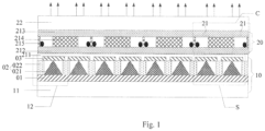
- Fig. 3 is a schematic cross-sectional view of a display component according to one embodiment of the present invention.
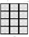
- Fig. 4 is a schematic top view of structure of a display component according to one embodiment of the present disclosure.
- Fig. 5 is a partial enlarged view of a display component according to an embodiment of the present invention.
- the greater the number of pixel units 120 in the display component the higher the resolution of the display component. Furthermore, in order to improve the resolution of the display component, the smaller the number of light-emitting pixels included in a pixel unit 120, the higher the resolution of the display component.
Landscapes
- Physics & Mathematics (AREA)
- Nonlinear Science (AREA)
- General Physics & Mathematics (AREA)
- Optics & Photonics (AREA)
- Chemical & Material Sciences (AREA)
- Crystallography & Structural Chemistry (AREA)
- Mathematical Physics (AREA)
- Geometry (AREA)
- Devices For Indicating Variable Information By Combining Individual Elements (AREA)
- Electroluminescent Light Sources (AREA)
- Electrochromic Elements, Electrophoresis, Or Variable Reflection Or Absorption Elements (AREA)
Claims (13)
- Anzeigekomponente, umfassend:ein Anzeigemodul (10);wobei das Anzeigemodul (10) eine Vielzahl von Spalten von lichtemittierenden Pixeln (12) auf einem Basissubstrat (11) umfasst, jedes der lichtemittierenden Pixel (12) umfassend eine erste Elektrodenschicht (01), eine Nanopartikelschicht (02) und eine zweite Elektrodenschicht (03), die Nanopartikelschicht (02) umfassend Nanopartikel (021) eines ersten Metalls, wobei jedes der Nanopartikel (021) des ersten Metalls einen konvexen Vorsprung auf einer von der ersten Elektrodenschicht (01) abgewandten Seite aufweist, und die zweite Elektrodenschicht (03) umfassend ein Ion eines zweiten Metalls;dadurch gekennzeichnet, dass das Anzeigemodul ferner ein Blickwinkelschaltmodul (20) an einer Lichtaustrittsseite des Anzeigemoduls (10) umfasst;wobei das Blickwinkelschaltmodul (20) eine Vielzahl von Blickwinkelsteuereinheiten (C) umfasst, jede der Vielzahl von Blickwinkelsteuereinheiten (C) umfassend zwei Blickwinkelsteuerabschnitte (21), die sich in eine Spaltenrichtung erstrecken, und wobei jeder der Blickwinkelsteuerabschnitte (21) einer Spalte der lichtemittierenden Pixel (12) entspricht; und wobeijeder der Blickwinkelsteuerungsabschnitte (21) eine Isolierschicht (211), die das Anzeigemodul (10) bedeckt, eine dritte Elektrodenschicht (212), eine vierte Elektrodenschicht (213) und einen Sperrabschnitt (214) zwischen der dritten Elektrodenschicht (212) und der vierten Elektrodenschicht (213) umfasst, und wobei eine Aufnahmekammer zwischen benachbarten Sperrabschnitten (214) gebildet ist und eine schwarze unpolare Flüssigkeit (215) in der Aufnahmekammer aufgenommen ist.
- Anzeigekomponente nach Anspruch 1, wobei das erste Metall Gold ist.
- Anzeigekomponente nach Anspruch 1 oder Anspruch 2, wobei das zweite Metall Silber ist.
- Anzeigekomponente nach einem der Ansprüche 1 bis 3, wobei der konvexe Vorsprung von Nanopartikeln (021) des ersten Metalls eine Kegelform oder eine Kegelstumpfform ist.
- Anzeigekomponente nach Anspruch 1, wobei jeweils zwei benachbarte Spalten von N Zeilen der lichtemittierenden Pixel (12) eine Pixeleinheit (120) darstellen, das Anzeigemodul (10) ferner eine schwarze Matrix (13) zwischen benachbarten Pixeleinheiten (120) umfasst, und N eine ganze Zahl größer als oder gleich wie 1 ist.
- Anzeigekomponente nach Anspruch 1, wobei
N eine ganze Zahl kleiner als oder gleich wie 5 ist. - Anzeigeelement nach Anspruch 1, wobei die Aufnahmekammer einer Spalte der lichtemittierenden Pixel (12) entspricht.
- Anzeigekomponente nach Anspruch 1 oder Anspruch 7, wobei die schwarze unpolare Flüssigkeit (215) konfiguriert ist, um bei Vorhandensein eines elektrischen Felds zwischen der dritten Elektrodenschicht (212) und der vierten Elektrodenschicht (213) die Aufnahmekammer zu bedecken und sich bei Abwesenheit eines elektrischen Felds zwischen der dritten Elektrodenschicht (212) und der vierten Elektrodenschicht (213) in einem Bereich zu sammeln, in dem die Aufnahmekammer und eine schwarze Matrix (13) überlappen.
- Anzeigekomponente nach Anspruch 1, wobei die Nanopartikelschicht (02) ferner eine Trennwand (022) umfasst, die konfiguriert ist, um die benachbarten Nanopartikel (021) des ersten Metalls zu trennen, und die Trennwand (022) ein Isoliermaterial umfasst;
optional das Isoliermaterial Siliziumdioxid ist. - Anzeigekomponente nach einem der Ansprüche 1-9, wobei die erste Elektrodenschicht (01) von jedem der lichtemittierenden Pixel (12) miteinander verbunden ist, um eine einheitliche Struktur zu bilden, oder die zweite Elektrodenschicht (03) von jedem der lichtemittierenden Pixel (12) miteinander verbunden ist, um eine einheitliche Struktur zu bilden.
- Anzeigekomponente nach Anspruch 1, wobei die dritte Elektrodenschicht (212) von jedem der Vielzahl von Blickwinkelsteuerungsabschnitten (21) miteinander verbunden ist, um eine einheitliche Struktur zu bilden, oder die vierte Elektrodenschicht (213) von jedem der Blickwinkelsteuerungsabschnitte (21) miteinander verbunden ist, um eine einheitliche Struktur zu bilden.
- Anzeigekomponente nach Anspruch 1, wobei jeder der Blickwinkelsteuerungsabschnitte (21) konfiguriert ist, um in einem ersten Anzeigemodus Licht durchzulassen, das von der entsprechenden Spalte der lichtemittierenden Pixel (12) emittiert wird, und in einem zweiten Anzeigemodus das Licht zu sperren, das von der entsprechenden Spalte der lichtemittierenden Pixel (12) emittiert wird und auf einer Seite von einer Spitze des konvexen Vorsprungs von Nanopartikeln (021) des ersten Metalls weg von der anderen Spalte der lichtemittierenden Pixel (12) in derselben Pixeleinheit (120) austritt.
- Anzeigevorrichtung, dadurch gekennzeichnet, dass sie die Anzeigekomponente nach einem der Ansprüche 1 bis 12 umfasst.
Applications Claiming Priority (2)
| Application Number | Priority Date | Filing Date | Title |
|---|---|---|---|
| CN201710738926.4A CN109445225B (zh) | 2017-08-24 | 2017-08-24 | 一种显示器件及显示装置 |
| PCT/CN2018/088184 WO2019037495A1 (en) | 2017-08-24 | 2018-05-24 | DISPLAY ELEMENT AND DISPLAY APPARATUS |
Publications (3)
| Publication Number | Publication Date |
|---|---|
| EP3673328A1 EP3673328A1 (de) | 2020-07-01 |
| EP3673328A4 EP3673328A4 (de) | 2021-05-19 |
| EP3673328B1 true EP3673328B1 (de) | 2023-07-19 |
Family
ID=65439372
Family Applications (1)
| Application Number | Title | Priority Date | Filing Date |
|---|---|---|---|
| EP18803305.4A Active EP3673328B1 (de) | 2017-08-24 | 2018-05-24 | Anzeigekomponente und anzeigevorrichtung |
Country Status (5)
| Country | Link |
|---|---|
| US (1) | US11215880B2 (de) |
| EP (1) | EP3673328B1 (de) |
| JP (1) | JP7434709B2 (de) |
| CN (1) | CN109445225B (de) |
| WO (1) | WO2019037495A1 (de) |
Families Citing this family (2)
| Publication number | Priority date | Publication date | Assignee | Title |
|---|---|---|---|---|
| CN112071279A (zh) * | 2020-09-16 | 2020-12-11 | 昆山龙腾光电股份有限公司 | 单双视角可切换的显示装置及控制方法 |
| WO2022246698A1 (zh) * | 2021-05-26 | 2022-12-01 | 华为技术有限公司 | 一种显示装置以及显示装置的调节方法 |
Family Cites Families (17)
| Publication number | Priority date | Publication date | Assignee | Title |
|---|---|---|---|---|
| JP2003330048A (ja) * | 2002-05-13 | 2003-11-19 | Canon Inc | 電気泳動表示装置 |
| KR101222957B1 (ko) * | 2005-12-29 | 2013-01-17 | 엘지디스플레이 주식회사 | 액정표시장치 |
| KR101013885B1 (ko) * | 2009-07-03 | 2011-02-14 | 한국기계연구원 | 유기 발광다이오드 및 유기 발광다이오드의 제조방법 |
| CN101968566A (zh) * | 2009-07-27 | 2011-02-09 | 胜华科技股份有限公司 | 电湿润显示器 |
| US8896907B2 (en) * | 2009-11-06 | 2014-11-25 | Sharp Laboratories Of America, Inc. | Plasmonic reflective display fabricated using anodized aluminum oxide |
| KR101741167B1 (ko) * | 2010-10-22 | 2017-05-30 | 삼성디스플레이 주식회사 | 유기 발광 표시 장치 |
| CN103728769B (zh) | 2012-10-11 | 2016-08-10 | 财团法人工业技术研究院 | 立体显示设备 |
| KR101440232B1 (ko) * | 2013-05-23 | 2014-09-12 | 삼성토탈 주식회사 | 이방성 금속 나노입자를 이용한 발광효율이 증대된 광변환 발광소자 |
| KR101499487B1 (ko) * | 2013-10-31 | 2015-03-18 | 한국과학기술연구원 | 플라즈모닉 나노 칼라 코팅층 및 이의 형성 방법 |
| US9625706B2 (en) * | 2014-07-31 | 2017-04-18 | Jsr Corporation | Display element, photosensitive composition and electrowetting display |
| CN104656249A (zh) * | 2015-03-19 | 2015-05-27 | 京东方科技集团股份有限公司 | 电润湿显示面板、制作方法和电润湿显示装置 |
| KR102607857B1 (ko) * | 2016-03-17 | 2023-11-29 | 삼성전자주식회사 | 코어쉘 구조의 나노 입자를 포함하는 발광 소자 |
| CN105911746B (zh) * | 2016-06-29 | 2017-10-13 | 京东方科技集团股份有限公司 | 显示装置及其视角切换方法 |
| CN105954901B (zh) * | 2016-07-12 | 2019-06-04 | 京东方科技集团股份有限公司 | 一种显示装置、制作方法和显示方法 |
| CN106450016B (zh) * | 2016-10-17 | 2019-11-12 | Tcl集团股份有限公司 | 一种发光器件及制备方法 |
| CN106773180A (zh) * | 2017-01-16 | 2017-05-31 | 京东方科技集团股份有限公司 | 视角切换结构和显示装置 |
| CN106873234B (zh) * | 2017-03-16 | 2019-10-25 | 京东方科技集团股份有限公司 | 发光显示器件及其制作方法、发光显示装置 |
-
2017
- 2017-08-24 CN CN201710738926.4A patent/CN109445225B/zh active Active
-
2018
- 2018-05-24 US US16/303,353 patent/US11215880B2/en active Active
- 2018-05-24 JP JP2018564778A patent/JP7434709B2/ja active Active
- 2018-05-24 WO PCT/CN2018/088184 patent/WO2019037495A1/en not_active Ceased
- 2018-05-24 EP EP18803305.4A patent/EP3673328B1/de active Active
Also Published As
| Publication number | Publication date |
|---|---|
| US11215880B2 (en) | 2022-01-04 |
| CN109445225A (zh) | 2019-03-08 |
| JP7434709B2 (ja) | 2024-02-21 |
| WO2019037495A1 (en) | 2019-02-28 |
| EP3673328A1 (de) | 2020-07-01 |
| CN109445225B (zh) | 2020-07-14 |
| US20210223636A1 (en) | 2021-07-22 |
| EP3673328A4 (de) | 2021-05-19 |
| JP2020531875A (ja) | 2020-11-05 |
Similar Documents
| Publication | Publication Date | Title |
|---|---|---|
| US11088213B1 (en) | Display substrate, display apparatus, method of controlling display substrate, and method of fabricating display substrate | |
| TWI385613B (zh) | Perspective display device | |
| US10372012B2 (en) | Mechanical chameleon through dynamic real-time plasmonic tuning | |
| DE112016001355T5 (de) | Anzeigevorrichtung, elektronisches Gerät und System | |
| US20130341659A1 (en) | Display panel | |
| TW202226215A (zh) | 顯示系統及資料處理方法 | |
| CN111679466B (zh) | 视角可切换的显示面板、显示装置及视角切换方法 | |
| WO2011058725A1 (ja) | 表示装置及びその製造方法 | |
| JP2016038490A (ja) | 表示パネル、表示モジュール、及び電子機器 | |
| US10824030B2 (en) | Grayscale control structure and method, liquid crystal display panel and display device | |
| EP3657238A1 (de) | Anzeigetafel | |
| CN111162104A (zh) | 彩色滤光片结构以及oled显示面板 | |
| US20160282650A1 (en) | Peep prevention display | |
| US20180241008A1 (en) | Self-light emitting display panel, and display device comprising same | |
| CN111613653A (zh) | 显示面板与显示设备 | |
| US11215880B2 (en) | Display component and display apparatus | |
| WO2016203340A1 (ja) | 表示装置の作製方法、表示装置、電子機器、プロジェクター、及びヘッドマウントディスプレイ | |
| CN102736309B (zh) | 显示面板、显示装置及电子设备 | |
| DE102017216169B4 (de) | Anzeigesystem und elektronische Vorrichtung | |
| EP4006620A1 (de) | Lichtroutensteuerungselement und anzeigevorrichtung damit | |
| US9122050B2 (en) | Electrowetting device | |
| KR101308079B1 (ko) | 표면 플라즈몬 컬러필터 | |
| JP7645409B2 (ja) | 表示装置 | |
| US9217884B2 (en) | Tunable photonic crystal color filter and color image display apparatus including the same | |
| CN117872651A (zh) | 一种显示面板、其控制方法及显示装置 |
Legal Events
| Date | Code | Title | Description |
|---|---|---|---|
| STAA | Information on the status of an ep patent application or granted ep patent |
Free format text: STATUS: UNKNOWN |
|
| STAA | Information on the status of an ep patent application or granted ep patent |
Free format text: STATUS: THE INTERNATIONAL PUBLICATION HAS BEEN MADE |
|
| PUAI | Public reference made under article 153(3) epc to a published international application that has entered the european phase |
Free format text: ORIGINAL CODE: 0009012 |
|
| STAA | Information on the status of an ep patent application or granted ep patent |
Free format text: STATUS: REQUEST FOR EXAMINATION WAS MADE |
|
| 17P | Request for examination filed |
Effective date: 20181126 |
|
| AK | Designated contracting states |
Kind code of ref document: A1 Designated state(s): AL AT BE BG CH CY CZ DE DK EE ES FI FR GB GR HR HU IE IS IT LI LT LU LV MC MK MT NL NO PL PT RO RS SE SI SK SM TR |
|
| AX | Request for extension of the european patent |
Extension state: BA ME |
|
| DAV | Request for validation of the european patent (deleted) | ||
| DAX | Request for extension of the european patent (deleted) | ||
| A4 | Supplementary search report drawn up and despatched |
Effective date: 20210415 |
|
| RIC1 | Information provided on ipc code assigned before grant |
Ipc: G02F 1/1335 20060101AFI20210409BHEP Ipc: B82Y 30/00 20110101ALI20210409BHEP Ipc: G02F 1/13 20060101ALI20210409BHEP Ipc: B82Y 20/00 20110101ALI20210409BHEP Ipc: H01L 51/52 20060101ALI20210409BHEP Ipc: H01L 51/50 20060101ALN20210409BHEP |
|
| REG | Reference to a national code |
Ref country code: DE Ref legal event code: R079 Free format text: PREVIOUS MAIN CLASS: G02F0001133500 Ipc: G02F0001170000 Ref document number: 602018053711 Country of ref document: DE |
|
| RIC1 | Information provided on ipc code assigned before grant |
Ipc: H10K 50/85 20230101ALI20230216BHEP Ipc: B82Y 20/00 20110101ALI20230216BHEP Ipc: G02F 1/13 20060101ALI20230216BHEP Ipc: B82Y 30/00 20110101ALI20230216BHEP Ipc: G02F 1/1335 20060101ALI20230216BHEP Ipc: G02F 1/17 20060101AFI20230216BHEP |
|
| GRAP | Despatch of communication of intention to grant a patent |
Free format text: ORIGINAL CODE: EPIDOSNIGR1 |
|
| STAA | Information on the status of an ep patent application or granted ep patent |
Free format text: STATUS: GRANT OF PATENT IS INTENDED |
|
| INTG | Intention to grant announced |
Effective date: 20230404 |
|
| GRAS | Grant fee paid |
Free format text: ORIGINAL CODE: EPIDOSNIGR3 |
|
| GRAA | (expected) grant |
Free format text: ORIGINAL CODE: 0009210 |
|
| STAA | Information on the status of an ep patent application or granted ep patent |
Free format text: STATUS: THE PATENT HAS BEEN GRANTED |
|
| AK | Designated contracting states |
Kind code of ref document: B1 Designated state(s): AL AT BE BG CH CY CZ DE DK EE ES FI FR GB GR HR HU IE IS IT LI LT LU LV MC MK MT NL NO PL PT RO RS SE SI SK SM TR |
|
| REG | Reference to a national code |
Ref country code: GB Ref legal event code: FG4D |
|
| REG | Reference to a national code |
Ref country code: CH Ref legal event code: EP |
|
| REG | Reference to a national code |
Ref country code: DE Ref legal event code: R096 Ref document number: 602018053711 Country of ref document: DE |
|
| REG | Reference to a national code |
Ref country code: IE Ref legal event code: FG4D |
|
| REG | Reference to a national code |
Ref country code: LT Ref legal event code: MG9D |
|
| REG | Reference to a national code |
Ref country code: NL Ref legal event code: MP Effective date: 20230719 |
|
| REG | Reference to a national code |
Ref country code: AT Ref legal event code: MK05 Ref document number: 1590061 Country of ref document: AT Kind code of ref document: T Effective date: 20230719 |
|
| PG25 | Lapsed in a contracting state [announced via postgrant information from national office to epo] |
Ref country code: NL Free format text: LAPSE BECAUSE OF FAILURE TO SUBMIT A TRANSLATION OF THE DESCRIPTION OR TO PAY THE FEE WITHIN THE PRESCRIBED TIME-LIMIT Effective date: 20230719 |
|
| PG25 | Lapsed in a contracting state [announced via postgrant information from national office to epo] |
Ref country code: GR Free format text: LAPSE BECAUSE OF FAILURE TO SUBMIT A TRANSLATION OF THE DESCRIPTION OR TO PAY THE FEE WITHIN THE PRESCRIBED TIME-LIMIT Effective date: 20231020 |
|
| PG25 | Lapsed in a contracting state [announced via postgrant information from national office to epo] |
Ref country code: IS Free format text: LAPSE BECAUSE OF FAILURE TO SUBMIT A TRANSLATION OF THE DESCRIPTION OR TO PAY THE FEE WITHIN THE PRESCRIBED TIME-LIMIT Effective date: 20231119 |
|
| PG25 | Lapsed in a contracting state [announced via postgrant information from national office to epo] |
Ref country code: SE Free format text: LAPSE BECAUSE OF FAILURE TO SUBMIT A TRANSLATION OF THE DESCRIPTION OR TO PAY THE FEE WITHIN THE PRESCRIBED TIME-LIMIT Effective date: 20230719 Ref country code: RS Free format text: LAPSE BECAUSE OF FAILURE TO SUBMIT A TRANSLATION OF THE DESCRIPTION OR TO PAY THE FEE WITHIN THE PRESCRIBED TIME-LIMIT Effective date: 20230719 Ref country code: PT Free format text: LAPSE BECAUSE OF FAILURE TO SUBMIT A TRANSLATION OF THE DESCRIPTION OR TO PAY THE FEE WITHIN THE PRESCRIBED TIME-LIMIT Effective date: 20231120 Ref country code: NO Free format text: LAPSE BECAUSE OF FAILURE TO SUBMIT A TRANSLATION OF THE DESCRIPTION OR TO PAY THE FEE WITHIN THE PRESCRIBED TIME-LIMIT Effective date: 20231019 Ref country code: LV Free format text: LAPSE BECAUSE OF FAILURE TO SUBMIT A TRANSLATION OF THE DESCRIPTION OR TO PAY THE FEE WITHIN THE PRESCRIBED TIME-LIMIT Effective date: 20230719 Ref country code: LT Free format text: LAPSE BECAUSE OF FAILURE TO SUBMIT A TRANSLATION OF THE DESCRIPTION OR TO PAY THE FEE WITHIN THE PRESCRIBED TIME-LIMIT Effective date: 20230719 Ref country code: IS Free format text: LAPSE BECAUSE OF FAILURE TO SUBMIT A TRANSLATION OF THE DESCRIPTION OR TO PAY THE FEE WITHIN THE PRESCRIBED TIME-LIMIT Effective date: 20231119 Ref country code: HR Free format text: LAPSE BECAUSE OF FAILURE TO SUBMIT A TRANSLATION OF THE DESCRIPTION OR TO PAY THE FEE WITHIN THE PRESCRIBED TIME-LIMIT Effective date: 20230719 Ref country code: GR Free format text: LAPSE BECAUSE OF FAILURE TO SUBMIT A TRANSLATION OF THE DESCRIPTION OR TO PAY THE FEE WITHIN THE PRESCRIBED TIME-LIMIT Effective date: 20231020 Ref country code: FI Free format text: LAPSE BECAUSE OF FAILURE TO SUBMIT A TRANSLATION OF THE DESCRIPTION OR TO PAY THE FEE WITHIN THE PRESCRIBED TIME-LIMIT Effective date: 20230719 Ref country code: AT Free format text: LAPSE BECAUSE OF FAILURE TO SUBMIT A TRANSLATION OF THE DESCRIPTION OR TO PAY THE FEE WITHIN THE PRESCRIBED TIME-LIMIT Effective date: 20230719 |
|
| PG25 | Lapsed in a contracting state [announced via postgrant information from national office to epo] |
Ref country code: PL Free format text: LAPSE BECAUSE OF FAILURE TO SUBMIT A TRANSLATION OF THE DESCRIPTION OR TO PAY THE FEE WITHIN THE PRESCRIBED TIME-LIMIT Effective date: 20230719 |
|
| REG | Reference to a national code |
Ref country code: DE Ref legal event code: R097 Ref document number: 602018053711 Country of ref document: DE |
|
| PG25 | Lapsed in a contracting state [announced via postgrant information from national office to epo] |
Ref country code: ES Free format text: LAPSE BECAUSE OF FAILURE TO SUBMIT A TRANSLATION OF THE DESCRIPTION OR TO PAY THE FEE WITHIN THE PRESCRIBED TIME-LIMIT Effective date: 20230719 |
|
| PG25 | Lapsed in a contracting state [announced via postgrant information from national office to epo] |
Ref country code: SM Free format text: LAPSE BECAUSE OF FAILURE TO SUBMIT A TRANSLATION OF THE DESCRIPTION OR TO PAY THE FEE WITHIN THE PRESCRIBED TIME-LIMIT Effective date: 20230719 Ref country code: RO Free format text: LAPSE BECAUSE OF FAILURE TO SUBMIT A TRANSLATION OF THE DESCRIPTION OR TO PAY THE FEE WITHIN THE PRESCRIBED TIME-LIMIT Effective date: 20230719 Ref country code: ES Free format text: LAPSE BECAUSE OF FAILURE TO SUBMIT A TRANSLATION OF THE DESCRIPTION OR TO PAY THE FEE WITHIN THE PRESCRIBED TIME-LIMIT Effective date: 20230719 Ref country code: EE Free format text: LAPSE BECAUSE OF FAILURE TO SUBMIT A TRANSLATION OF THE DESCRIPTION OR TO PAY THE FEE WITHIN THE PRESCRIBED TIME-LIMIT Effective date: 20230719 Ref country code: DK Free format text: LAPSE BECAUSE OF FAILURE TO SUBMIT A TRANSLATION OF THE DESCRIPTION OR TO PAY THE FEE WITHIN THE PRESCRIBED TIME-LIMIT Effective date: 20230719 Ref country code: CZ Free format text: LAPSE BECAUSE OF FAILURE TO SUBMIT A TRANSLATION OF THE DESCRIPTION OR TO PAY THE FEE WITHIN THE PRESCRIBED TIME-LIMIT Effective date: 20230719 Ref country code: SK Free format text: LAPSE BECAUSE OF FAILURE TO SUBMIT A TRANSLATION OF THE DESCRIPTION OR TO PAY THE FEE WITHIN THE PRESCRIBED TIME-LIMIT Effective date: 20230719 |
|
| PLBE | No opposition filed within time limit |
Free format text: ORIGINAL CODE: 0009261 |
|
| STAA | Information on the status of an ep patent application or granted ep patent |
Free format text: STATUS: NO OPPOSITION FILED WITHIN TIME LIMIT |
|
| PG25 | Lapsed in a contracting state [announced via postgrant information from national office to epo] |
Ref country code: IT Free format text: LAPSE BECAUSE OF FAILURE TO SUBMIT A TRANSLATION OF THE DESCRIPTION OR TO PAY THE FEE WITHIN THE PRESCRIBED TIME-LIMIT Effective date: 20230719 |
|
| 26N | No opposition filed |
Effective date: 20240422 |
|
| PG25 | Lapsed in a contracting state [announced via postgrant information from national office to epo] |
Ref country code: SI Free format text: LAPSE BECAUSE OF FAILURE TO SUBMIT A TRANSLATION OF THE DESCRIPTION OR TO PAY THE FEE WITHIN THE PRESCRIBED TIME-LIMIT Effective date: 20230719 |
|
| PG25 | Lapsed in a contracting state [announced via postgrant information from national office to epo] |
Ref country code: BG Free format text: LAPSE BECAUSE OF FAILURE TO SUBMIT A TRANSLATION OF THE DESCRIPTION OR TO PAY THE FEE WITHIN THE PRESCRIBED TIME-LIMIT Effective date: 20230719 |
|
| PG25 | Lapsed in a contracting state [announced via postgrant information from national office to epo] |
Ref country code: BG Free format text: LAPSE BECAUSE OF FAILURE TO SUBMIT A TRANSLATION OF THE DESCRIPTION OR TO PAY THE FEE WITHIN THE PRESCRIBED TIME-LIMIT Effective date: 20230719 |
|
| REG | Reference to a national code |
Ref country code: CH Ref legal event code: PL |
|
| PG25 | Lapsed in a contracting state [announced via postgrant information from national office to epo] |
Ref country code: MC Free format text: LAPSE BECAUSE OF FAILURE TO SUBMIT A TRANSLATION OF THE DESCRIPTION OR TO PAY THE FEE WITHIN THE PRESCRIBED TIME-LIMIT Effective date: 20230719 |
|
| PG25 | Lapsed in a contracting state [announced via postgrant information from national office to epo] |
Ref country code: LU Free format text: LAPSE BECAUSE OF NON-PAYMENT OF DUE FEES Effective date: 20240524 |
|
| GBPC | Gb: european patent ceased through non-payment of renewal fee |
Effective date: 20240524 |
|
| PG25 | Lapsed in a contracting state [announced via postgrant information from national office to epo] |
Ref country code: MC Free format text: LAPSE BECAUSE OF FAILURE TO SUBMIT A TRANSLATION OF THE DESCRIPTION OR TO PAY THE FEE WITHIN THE PRESCRIBED TIME-LIMIT Effective date: 20230719 Ref country code: LU Free format text: LAPSE BECAUSE OF NON-PAYMENT OF DUE FEES Effective date: 20240524 Ref country code: CH Free format text: LAPSE BECAUSE OF NON-PAYMENT OF DUE FEES Effective date: 20240531 |
|
| REG | Reference to a national code |
Ref country code: BE Ref legal event code: MM Effective date: 20240531 |
|
| PG25 | Lapsed in a contracting state [announced via postgrant information from national office to epo] |
Ref country code: IE Free format text: LAPSE BECAUSE OF NON-PAYMENT OF DUE FEES Effective date: 20240524 |
|
| PG25 | Lapsed in a contracting state [announced via postgrant information from national office to epo] |
Ref country code: BE Free format text: LAPSE BECAUSE OF NON-PAYMENT OF DUE FEES Effective date: 20240531 |
|
| PG25 | Lapsed in a contracting state [announced via postgrant information from national office to epo] |
Ref country code: FR Free format text: LAPSE BECAUSE OF NON-PAYMENT OF DUE FEES Effective date: 20240531 |
|
| PG25 | Lapsed in a contracting state [announced via postgrant information from national office to epo] |
Ref country code: GB Free format text: LAPSE BECAUSE OF NON-PAYMENT OF DUE FEES Effective date: 20240524 |
|
| PGFP | Annual fee paid to national office [announced via postgrant information from national office to epo] |
Ref country code: DE Payment date: 20250519 Year of fee payment: 8 |
|
| PG25 | Lapsed in a contracting state [announced via postgrant information from national office to epo] |
Ref country code: CY Free format text: LAPSE BECAUSE OF FAILURE TO SUBMIT A TRANSLATION OF THE DESCRIPTION OR TO PAY THE FEE WITHIN THE PRESCRIBED TIME-LIMIT; INVALID AB INITIO Effective date: 20180524 |
|
| PG25 | Lapsed in a contracting state [announced via postgrant information from national office to epo] |
Ref country code: HU Free format text: LAPSE BECAUSE OF FAILURE TO SUBMIT A TRANSLATION OF THE DESCRIPTION OR TO PAY THE FEE WITHIN THE PRESCRIBED TIME-LIMIT; INVALID AB INITIO Effective date: 20180524 |