EP3673328B1 - Display component and display apparatus - Google Patents
Display component and display apparatus Download PDFInfo
- Publication number
- EP3673328B1 EP3673328B1 EP18803305.4A EP18803305A EP3673328B1 EP 3673328 B1 EP3673328 B1 EP 3673328B1 EP 18803305 A EP18803305 A EP 18803305A EP 3673328 B1 EP3673328 B1 EP 3673328B1
- Authority
- EP
- European Patent Office
- Prior art keywords
- electrode layer
- display
- display component
- light
- metal
- Prior art date
- Legal status (The legal status is an assumption and is not a legal conclusion. Google has not performed a legal analysis and makes no representation as to the accuracy of the status listed.)
- Active
Links
Images



Classifications
-
- G—PHYSICS
- G02—OPTICS
- G02F—OPTICAL DEVICES OR ARRANGEMENTS FOR THE CONTROL OF LIGHT BY MODIFICATION OF THE OPTICAL PROPERTIES OF THE MEDIA OF THE ELEMENTS INVOLVED THEREIN; NON-LINEAR OPTICS; FREQUENCY-CHANGING OF LIGHT; OPTICAL LOGIC ELEMENTS; OPTICAL ANALOGUE/DIGITAL CONVERTERS
- G02F1/00—Devices or arrangements for the control of the intensity, colour, phase, polarisation or direction of light arriving from an independent light source, e.g. switching, gating or modulating; Non-linear optics
- G02F1/01—Devices or arrangements for the control of the intensity, colour, phase, polarisation or direction of light arriving from an independent light source, e.g. switching, gating or modulating; Non-linear optics for the control of the intensity, phase, polarisation or colour
- G02F1/17—Devices or arrangements for the control of the intensity, colour, phase, polarisation or direction of light arriving from an independent light source, e.g. switching, gating or modulating; Non-linear optics for the control of the intensity, phase, polarisation or colour based on variable-absorption elements not provided for in groups G02F1/015 - G02F1/169
-
- G—PHYSICS
- G02—OPTICS
- G02F—OPTICAL DEVICES OR ARRANGEMENTS FOR THE CONTROL OF LIGHT BY MODIFICATION OF THE OPTICAL PROPERTIES OF THE MEDIA OF THE ELEMENTS INVOLVED THEREIN; NON-LINEAR OPTICS; FREQUENCY-CHANGING OF LIGHT; OPTICAL LOGIC ELEMENTS; OPTICAL ANALOGUE/DIGITAL CONVERTERS
- G02F1/00—Devices or arrangements for the control of the intensity, colour, phase, polarisation or direction of light arriving from an independent light source, e.g. switching, gating or modulating; Non-linear optics
- G02F1/01—Devices or arrangements for the control of the intensity, colour, phase, polarisation or direction of light arriving from an independent light source, e.g. switching, gating or modulating; Non-linear optics for the control of the intensity, phase, polarisation or colour
- G02F1/13—Devices or arrangements for the control of the intensity, colour, phase, polarisation or direction of light arriving from an independent light source, e.g. switching, gating or modulating; Non-linear optics for the control of the intensity, phase, polarisation or colour based on liquid crystals, e.g. single liquid crystal display cells
- G02F1/1323—Arrangements for providing a switchable viewing angle
-
- G—PHYSICS
- G02—OPTICS
- G02F—OPTICAL DEVICES OR ARRANGEMENTS FOR THE CONTROL OF LIGHT BY MODIFICATION OF THE OPTICAL PROPERTIES OF THE MEDIA OF THE ELEMENTS INVOLVED THEREIN; NON-LINEAR OPTICS; FREQUENCY-CHANGING OF LIGHT; OPTICAL LOGIC ELEMENTS; OPTICAL ANALOGUE/DIGITAL CONVERTERS
- G02F1/00—Devices or arrangements for the control of the intensity, colour, phase, polarisation or direction of light arriving from an independent light source, e.g. switching, gating or modulating; Non-linear optics
- G02F1/01—Devices or arrangements for the control of the intensity, colour, phase, polarisation or direction of light arriving from an independent light source, e.g. switching, gating or modulating; Non-linear optics for the control of the intensity, phase, polarisation or colour
- G02F1/13—Devices or arrangements for the control of the intensity, colour, phase, polarisation or direction of light arriving from an independent light source, e.g. switching, gating or modulating; Non-linear optics for the control of the intensity, phase, polarisation or colour based on liquid crystals, e.g. single liquid crystal display cells
- G02F1/133—Constructional arrangements; Operation of liquid crystal cells; Circuit arrangements
- G02F1/1333—Constructional arrangements; Manufacturing methods
- G02F1/1335—Structural association of cells with optical devices, e.g. polarisers or reflectors
- G02F1/133509—Filters, e.g. light shielding masks
- G02F1/133512—Light shielding layers, e.g. black matrix
-
- G—PHYSICS
- G02—OPTICS
- G02F—OPTICAL DEVICES OR ARRANGEMENTS FOR THE CONTROL OF LIGHT BY MODIFICATION OF THE OPTICAL PROPERTIES OF THE MEDIA OF THE ELEMENTS INVOLVED THEREIN; NON-LINEAR OPTICS; FREQUENCY-CHANGING OF LIGHT; OPTICAL LOGIC ELEMENTS; OPTICAL ANALOGUE/DIGITAL CONVERTERS
- G02F1/00—Devices or arrangements for the control of the intensity, colour, phase, polarisation or direction of light arriving from an independent light source, e.g. switching, gating or modulating; Non-linear optics
- G02F1/01—Devices or arrangements for the control of the intensity, colour, phase, polarisation or direction of light arriving from an independent light source, e.g. switching, gating or modulating; Non-linear optics for the control of the intensity, phase, polarisation or colour
- G02F1/13—Devices or arrangements for the control of the intensity, colour, phase, polarisation or direction of light arriving from an independent light source, e.g. switching, gating or modulating; Non-linear optics for the control of the intensity, phase, polarisation or colour based on liquid crystals, e.g. single liquid crystal display cells
- G02F1/133—Constructional arrangements; Operation of liquid crystal cells; Circuit arrangements
- G02F1/1333—Constructional arrangements; Manufacturing methods
- G02F1/1343—Electrodes
- G02F1/134309—Electrodes characterised by their geometrical arrangement
-
- H—ELECTRICITY
- H10—SEMICONDUCTOR DEVICES; ELECTRIC SOLID-STATE DEVICES NOT OTHERWISE PROVIDED FOR
- H10K—ORGANIC ELECTRIC SOLID-STATE DEVICES
- H10K59/00—Integrated devices, or assemblies of multiple devices, comprising at least one organic light-emitting element covered by group H10K50/00
- H10K59/80—Constructional details
- H10K59/875—Arrangements for extracting light from the devices
-
- B—PERFORMING OPERATIONS; TRANSPORTING
- B82—NANOTECHNOLOGY
- B82Y—SPECIFIC USES OR APPLICATIONS OF NANOSTRUCTURES; MEASUREMENT OR ANALYSIS OF NANOSTRUCTURES; MANUFACTURE OR TREATMENT OF NANOSTRUCTURES
- B82Y20/00—Nanooptics, e.g. quantum optics or photonic crystals
-
- B—PERFORMING OPERATIONS; TRANSPORTING
- B82—NANOTECHNOLOGY
- B82Y—SPECIFIC USES OR APPLICATIONS OF NANOSTRUCTURES; MEASUREMENT OR ANALYSIS OF NANOSTRUCTURES; MANUFACTURE OR TREATMENT OF NANOSTRUCTURES
- B82Y30/00—Nanotechnology for materials or surface science, e.g. nanocomposites
-
- G—PHYSICS
- G02—OPTICS
- G02F—OPTICAL DEVICES OR ARRANGEMENTS FOR THE CONTROL OF LIGHT BY MODIFICATION OF THE OPTICAL PROPERTIES OF THE MEDIA OF THE ELEMENTS INVOLVED THEREIN; NON-LINEAR OPTICS; FREQUENCY-CHANGING OF LIGHT; OPTICAL LOGIC ELEMENTS; OPTICAL ANALOGUE/DIGITAL CONVERTERS
- G02F2202/00—Materials and properties
- G02F2202/36—Micro- or nanomaterials
-
- G—PHYSICS
- G02—OPTICS
- G02F—OPTICAL DEVICES OR ARRANGEMENTS FOR THE CONTROL OF LIGHT BY MODIFICATION OF THE OPTICAL PROPERTIES OF THE MEDIA OF THE ELEMENTS INVOLVED THEREIN; NON-LINEAR OPTICS; FREQUENCY-CHANGING OF LIGHT; OPTICAL LOGIC ELEMENTS; OPTICAL ANALOGUE/DIGITAL CONVERTERS
- G02F2203/00—Function characteristic
- G02F2203/10—Function characteristic plasmon
-
- H—ELECTRICITY
- H10—SEMICONDUCTOR DEVICES; ELECTRIC SOLID-STATE DEVICES NOT OTHERWISE PROVIDED FOR
- H10K—ORGANIC ELECTRIC SOLID-STATE DEVICES
- H10K50/00—Organic light-emitting devices
- H10K50/10—OLEDs or polymer light-emitting diodes [PLED]
- H10K50/11—OLEDs or polymer light-emitting diodes [PLED] characterised by the electroluminescent [EL] layers
- H10K50/115—OLEDs or polymer light-emitting diodes [PLED] characterised by the electroluminescent [EL] layers comprising active inorganic nanostructures, e.g. luminescent quantum dots
-
- H—ELECTRICITY
- H10—SEMICONDUCTOR DEVICES; ELECTRIC SOLID-STATE DEVICES NOT OTHERWISE PROVIDED FOR
- H10K—ORGANIC ELECTRIC SOLID-STATE DEVICES
- H10K59/00—Integrated devices, or assemblies of multiple devices, comprising at least one organic light-emitting element covered by group H10K50/00
- H10K59/30—Devices specially adapted for multicolour light emission
- H10K59/35—Devices specially adapted for multicolour light emission comprising red-green-blue [RGB] subpixels
-
- H—ELECTRICITY
- H10—SEMICONDUCTOR DEVICES; ELECTRIC SOLID-STATE DEVICES NOT OTHERWISE PROVIDED FOR
- H10K—ORGANIC ELECTRIC SOLID-STATE DEVICES
- H10K59/00—Integrated devices, or assemblies of multiple devices, comprising at least one organic light-emitting element covered by group H10K50/00
- H10K59/80—Constructional details
- H10K59/8791—Arrangements for improving contrast, e.g. preventing reflection of ambient light
- H10K59/8792—Arrangements for improving contrast, e.g. preventing reflection of ambient light comprising light absorbing layers, e.g. black layers
Definitions
- Fig. 3 is a schematic cross-sectional view of a display component according to one embodiment of the present invention.
- Fig. 4 is a schematic top view of structure of a display component according to one embodiment of the present disclosure.
- Fig. 5 is a partial enlarged view of a display component according to an embodiment of the present invention.
- the greater the number of pixel units 120 in the display component the higher the resolution of the display component. Furthermore, in order to improve the resolution of the display component, the smaller the number of light-emitting pixels included in a pixel unit 120, the higher the resolution of the display component.
Landscapes
- Physics & Mathematics (AREA)
- Nonlinear Science (AREA)
- General Physics & Mathematics (AREA)
- Optics & Photonics (AREA)
- Chemical & Material Sciences (AREA)
- Crystallography & Structural Chemistry (AREA)
- Mathematical Physics (AREA)
- Geometry (AREA)
- Devices For Indicating Variable Information By Combining Individual Elements (AREA)
- Electroluminescent Light Sources (AREA)
- Electrochromic Elements, Electrophoresis, Or Variable Reflection Or Absorption Elements (AREA)
Description
- The present invention relates to display technology and, more particularly, to a display component and a display apparatus.
- Dual view display mode refers to display of different images in different angles. That is, a user can view different images on a display screen from different angles. Compared to traditional display modes, dual view display mode increases utilization of the display screen, allowing a display screen to display two kinds of information at the same time. Currently, there has been great interest in dual-view display mode especially for applications such as cars and advertising screens.
-
CN 106873234 A discloses a light emitting display device, manufacturing method thereof and light emitting display equipment. The light emitting display device is composed of elements which are precisely compounded with the metal nanoparticles through electro-deposition and electro-corrosion so as to adjust the LSPR (Local Surface Plasmon Resonance) for compounding the metal nanoparticles, accordingly visible light absorption and scattering of the metal nanoparticles are continuously adjusted. - A display component and a display apparatus according to the invention are provided in the present disclosure, as defined in the appended set of claims.
- The subject matter which is regarded as the invention is particularly pointed out and distinctly claimed in the claims at the conclusion of the specification. The foregoing and other objects, features, and advantages of the invention are apparent from the following detailed description taken in conjunction with the accompanying drawings in which:
-
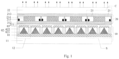
Fig. 1 is a schematic cross-sectional view of a display component according to one embodiment of the present invention; -
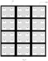
Fig. 2 is a schematic top view of structure of a display component according to one embodiment of the present invention; -
Fig. 3 is a schematic cross-sectional view of a display component according to one embodiment of the present invention; -
Fig. 4 is a schematic top view of structure of a display component according to one embodiment of the present invention; -
Fig. 5 is a partial enlarged view of a display component according to one embodiment of the present invention; -
Fig. 6 is a schematic cross-sectional view of a display component according to one embodiment of the present invention; -
Fig. 7 is a schematic top view of a display component according to one embodiment of the present invention; -
Fig. 8 is a schematic diagram of a display component in a first display mode according to one embodiment of the present invention; -
Fig. 9 is a schematic diagram of a display component in a second display mode according to one embodiment of the present invention; - The present invention will be described in further detail with reference to the accompanying drawings and embodiments in order to provide a better understanding by those skilled in the art of the technical solutions of the present invention. Throughout the description of the disclosure, reference is made to
Figs. 1-9 . When referring to the figures, like structures and elements shown throughout are indicated with like reference numerals. The described embodiments are merely some but not all of the embodiments of the present invention. All other embodiments obtained by persons of ordinary skill in the art based on the embodiments of the present invention without creative effort shall fall within the protection scope of the present invention, insofar they fall within the scope of the appended claims. Shapes and sizes of the display components in the drawings do not reflect the true scale, and are only intended to illustrate the present invention. - In this specification, the terms "first," "second," "third," and "fourth" may be added as prefixes. These prefixes, however, are only added in order to distinguish the terms and do not have specific meaning such as order and relative merits.
- "Metallic nanomaterials" are materials composed of a structure having at least one dimension within a three-dimensional space in a nanometer scale range (1 to 100nm) or materials composed of the nanostructure as basic units. The nano-dimensional features of the metallic nanomaterials make them different from both microscopic atoms and traditional bulk metal and crystalline materials. The metallic nanomaterials possess special physical and chemical properties due to surface effect, small size effect, quantum size effect and macroscopic quantum tunneling effect.
- When an incident light is irradiated onto a metal nanoparticle whose size is much smaller than a wavelength of light, if the frequency of the incident photon is equal or comparable to an oscillation frequency of an electron on the surface of the metal nanoparticle, the electron and the incident photon strongly resonate on a local surface area of the metal nanoparticle. This phenomenon is termed Local Surface Plasmon Resonance effect (LSPR). When the LSPR occurs on the surface of metal nanoparticles, the metal nanoparticles strongly absorb energy of the incident photons having the same or comparable oscillation frequency of the electrons or radiate electromagnetic wave having the same or comparable oscillation frequency of the electrons. That is, these properties are termed LSPR absorption or LSPR scattering, respectively.
- However, the LSPR properties of metal nanoparticles are closely related to their elemental composition. A display component according to one embodiment of the present disclosure precisely composes elemental composition of the metal nanoparticles by electrodeposition and/or electroerosion so as to adjust LSPR properties of the metal nanoparticles, and accordingly continuously adjusts absorption and scattering of visible light by the metal nanoparticles. As such, a color display having no polarization and no color film can be realized.
- As shown in
Fig. 1 to Fig. 5 of the present application, one example of the present invention is a display component. The display component comprises adisplay module 10 and a viewingangle switching module 20 located at a light-existing side of thedisplay module 10. -
Fig. 1 is a schematic cross-sectional view of a display component according to one embodiment of the present invention.Fig. 2 is a schematic top view of structure of a display component according to one embodiment of the present invention. - In one embodiment, as shown in
Fig. 1 , thedisplay module 10 comprises: abase substrate 11 and a plurality of light-emitting pixels 12 arranged in a matrix on thebase substrate 11. The light-emittingpixel 12 includes, in accordance with the invention, afirst electrode layer 01, ananoparticle layer 02, and a secondtransparent electrode layer 03 sequentially disposed on thebase substrate 11. Thenanoparticle layer 02 contains, further in accordance with the invention, nanoparticles of afirst metal 021. The nanoparticle of thefirst metal 021 has a convex protrusion on a side away from thefirst electrode layer 01. Thesecond electrode layer 03 contains, according to the invention, an ion of a second metal. In one embodiment, thesecond electrode layer 03 contains a nanoparticle of a second metal. - As shown in
Fig. 1 andFig. 2 , every two adjacent columns of light-emittingpixels 12 constitute a pixel group S. The viewingangle switch module 20 includes a plurality of viewing angle control units C, each of the viewing angle angel control units corresponding to one of the pixel groups S. According to the invention, the viewing angle control unit C includes two viewingangle control sections 21 extending in a column direction, whereby a viewingangle control section 21 corresponds to one column of light-emitting pixels 12. As shown inFig. 1 andFig. 2 , in a first display mode, the viewingangle control section 21 is configured to transmit light emitted by the corresponding column oflight emitting pixels 12. -
Fig. 3 is a schematic cross-sectional view of a display component according to one embodiment of the present invention.Fig. 4 is a schematic top view of structure of a display component according to one embodiment of the present disclosure.Fig. 5 is a partial enlarged view of a display component according to an embodiment of the present invention. - As shown in
Fig. 3 to Fig. 5 , in a second display mode, the viewingangle control section 21 is configured to block light emitted by the corresponding column of light emitting pixels and exiting on a side from the peak of the convex protrusion of the nanoparticles of thefirst metal 021 away from the other column of the light emitting pixels in the same pixel group S. For example, as shown inFig. 5 , the viewingangle control section 21 on the left side blocks the light of the leftlight emitting pixel 12 exiting from the left side of the peak O of the convex protrusion. The viewingangle control section 21 on the right side blocks the light of the rightlight emitting pixel 12 exiting from the right side of the peak O of the convex protrusion. - In the display component according to one embodiment of the present invention, because the nanoparticles of the first metal in the display module have the convex protrusion on the side away from the first electrode layer, the light can be emitted from different angles. By adjusting blocking state of the viewing angle control section in the viewing angle switch module, a dual view display mode as well as a traditional display mode can be realized. Furthermore, since the nanoparticles of the first metal are at nanoscale, their particle sizes are so small, and accordingly ultra-high resolution display can be achieved.
- In the display component provided by one embodiment of the present invention, without being held to a particular theory, it is believed that the display principle of the display module may be as follows: when electricity is applied between the first electrode layer, the nanoparticle layer, and the second electrode layer, ions of the second metal are reduced to the second metal, and the second metal is then deposited onto surface of nanoparticles of the first metal to form composite metal nanoparticles. In another embodiment, the second metal on the surface of nanoparticles of the first metal is oxidized to ions of the second metal, and the ions of the second metal are formed on the second electrode layer. That is, the elemental composition of the composite metal nanoparticles is controlled by electrodeposition (second metal reduction) and electroerosion (the second metal is oxidized) to adjust the LSPR properties of the composite metal nanoparticles so as to continuously adjust absorption and scattering of the visible light by the composite metal nanoparticles to realize a color display with fast response, no polarization, and no color film.
- Furthermore, in the display component according to one embodiment of the present invention, when a static image is displayed, since there is no requirement of constant flipping of liquid crystals as in a liquid crystal display component, power consumption is relatively low.
- In the display component provided by one embodiment of the present invention, the first display mode refers to a traditional display mode, that is, the same display image can be viewed regardless of whether a person is at any side of the display component. The second display mode refers to a dual view display mode, that is, a person who is on the left side of the display component and a person on the right side of the display component can view different display images.
- In the display component provided by one embodiment of the present invention, as shown in
Fig. 1 andFig. 3 , thenanoparticle layer 02 includes, in accordance with the invention,nanoparticles 021 of a first metal, and apartition wall 022 for separatingadjacent nanoparticles 021 of the first metal. Thewall 022 may be made of an insulating material so as to ensure independence between thenanoparticles 021 of the first metal while maintaining stable properties and also allowing an efficient electrochemical reaction between the first metal and the second metal. - In one embodiment, the partition wall can be formed by forming passing holes in a film layer, and a nanoparticle of a first metal is placed in each of the passing holes. In one embodiment, the partition wall is made of silicon dioxide. Of course, the partition wall can also be made of other insulating material and not limited thereto.
-
Fig. 6 is a schematic cross-sectional view of a display component according to one embodiment of the present invention.Fig. 7 is a schematic top view of structure of a display component according to one embodiment of the present invention. - In one embodiment, in order to prevent color mixing, in the display component provided by one embodiment of the present invention, as shown in
Fig. 6 andFig. 7 , thedisplay module 10 includes two columns of N rows ofpixels 12 as onepixel unit 120, and thedisplay module 10 further includes ablack matrix 13 located betweenadjacent pixel units 120. N is an integer greater than or equal to 1. -
Fig. 8 is a schematic diagram of a display component in a first display mode according to one embodiment of the present invention.Fig. 9 is a schematic diagram of a display component in a second display mode according to one embodiment of the present invention. - In one embodiment, in order to prevent color mixing, in the display component provided by one embodiment of the present invention, as shown in
Fig. 8 , in the first display mode, the light-emittingpixels 12 of onepixel unit 120 serve as one sub-pixel of the display component, such as a red sub-pixel, a green sub-pixel or a blue sub-pixel. Adjacent sub-pixels are separated by ablack matrix 13. As shown inFig. 9 , in the second display mode, a column of the light-emittingpixels 12 in onepixel unit 120 functions as one sub-pixel, such as a red sub-pixel, a green sub-pixel or a blue sub-pixel. From one of the dual viewing angles, the adjacent sub-pixels are separated by theblack matrix 13. Therefore, with a fixed panel size, the greater the number ofpixel units 120 in the display component, the higher the resolution of the display component. Furthermore, in order to improve the resolution of the display component, the smaller the number of light-emitting pixels included in apixel unit 120, the higher the resolution of the display component. - In one embodiment, in the display component provided by one embodiment of the present disclosure, N is smaller than or equal to 5.
- In the display component provided by one embodiment of the present invention, the first metal is gold and the second metal is silver. Since the LSPR properties of the metal nanoparticles are closely related to their elemental compositions, the gold-silver composite metal nanoparticles are used as the light-emitting materials in one embodiment of the present invention. When the content of gold in the composite metal nanoparticles gradually increases, the extinction spectrum thereof gradually moves toward longer wavelengths and can be utilized in the light-emitting component.
- In one embodiment, in the display component provided by one embodiment of the present invention, the second electrode layer is a gel electrode containing an ion of a second metal to facilitate efficient electrochemical reaction between the first metal and the second metal. Furthermore, when the second metal is silver, the light emitting performance of the light emitting component can be improved.
- In one embodiment, in the display component provided by one embodiment of the present invention, as shown in
Fig. 1 ,Fig. 3 , andFig. 6 , the second electrode layers 03 are arranged in a matrix. All the first electrode layers 01 are connected into a unitary structure, that is, thefirst electrode layer 01 has a whole layer structure. As such, the patterning process for the first electrode layer can be omitted, and wirings for providing signals to the first electrode layer can be reduced, thereby reducing cost. - In the display component provided by one embodiment of the present invention, the first electrode layers may also be arranged in a matrix. All the second electrode layers are connected into a unitary structure, that is, the second electrode layer has a whole layer structure. As such, the patterning process for the second electrode layer can be omitted, and wirings for providing signals to the second electrode layer can be reduced, thereby reducing cost.
- In one embodiment, the first electrode layers may also be arranged in a matrix, and the second electrode layers may be arranged in a matrix, which is not limited.
- In the display component provided by one embodiment of the present invention, as shown in
Fig. 1 ,Fig. 3 , andFig. 6 , the convex protrusion ofnanoparticles 021 of the first metal on a side away from thefirst electrode layer 01 is a cone shape, and the tapered peak portion of the cone shape is directed to thesecond electrode layer 03. This is conducive to uniform light-emitting on both sides of the light-emitting pixel. The convex protrusion of nanoparticles of the first metal could be other shapes such as a truncated cone. - In the display component provided by the present invention, as shown in
Fig. 1 ,Fig. 3 , andFig. 6 , the viewingangle control section 21 includes an insulatinglayer 211 covering thedisplay module 10, athird electrode layer 212 and afourth electrode layer 213 in preferably this order on the insulatinglayer 211, and a blockingportion 214 located between thethird electrode layer 212 and thefourth electrode layer 213. An accommodating chamber is formed between theadjacent blocking portions 214, and a black non-polar liquid 215 is accommodated in the accommodating chamber. - In one embodiment, when an electric field is applied between the
third electrode layer 212 and thefourth electrode layer 213, the black non-polar liquid 215 covers the accommodating chamber. Through the spread black nonpolar liquid 215, the viewingangle control section 21 blocks light from the corresponding column of thelight emitting pixels 12 exiting on a side from the peak of the protrusion of thenanoparticle 021 of the first metal away from the other column of thelight emitting pixels 12 in the same pixel group S. As such, the second display mode is realized. - In another embodiment, when there is no electric field between the
third electrode layer 212 and thefourth electrode layer 213, the black nonpolar liquid 215 collects in a region where the accommodating chamber and the black matrix overlap. As such, the viewingangle control section 21 transmits the light emitted by the corresponding column of the light-emittingpixels 12 to realize the first display mode. - In the display component provided by one embodiment of the present invention, the blocking
portion 214 is a transparent insulating material. - In the display component provided by one embodiment of the present invention, an accommodating chamber between the blocking portions corresponds to a light-emitting pixel. As such, it is easy to control action of the black non-polar liquid in the accommodating chamber, thereby improving control accuracy of the viewing angle control section.
- In the display component provided by one embodiment of the present invention, as shown in
Fig. 1 ,Fig. 3 , andFig. 6 , all the third electrode layers 212 are connected into a unitary structure. That is, thethird electrode layer 212 has a whole layer structure. As such, the patterning process for thethird electrode layer 212 can be omitted, and wirings for providing signals to thethird electrode layer 212 can be reduced, thereby reducing cost. - In the display component provided by one embodiment of the present invention, as shown in
Fig. 1 ,Fig. 3 , andFig. 6 , all the fourth electrode layers 213 are connected into a unitary structure. That is, thefourth electrode layer 213 has a whole layer structure. As such, the patterning process for thefourth electrode layer 213 can be omitted, and wirings for providing signals to thefourth electrode layer 213 can be reduced, thereby reducing cost. - In the display component provided by one embodiment of the present invention, the
third electrode layer 212 and thefourth electrode layer 213 may also be intermittent electrode structures, which are not specifically limited herein. - In the display component provided by one embodiment of the present invention, as shown in
Fig. 1 ,Fig. 3 , andFig. 6 , apackage protection layer 22 is provided at a side of the viewingangle switch module 20 away from thedisplay module 10 so as to protect the viewangle switch module 20 and thedisplay module 10. - Another example of the present invention is a display apparatus comprising the display component according to one embodiment of the present application. The display apparatus may be a mobile phone, a tablet, a television, a monitor, a notebook, a digital photo frame, a navigator, or any product or component that has a display function. For the implementation of the display apparatus, reference may be made to the foregoing embodiment of the display components, and details are not described herein again.
- Without being held to a particular theory, it is believed that, in the display component and the display apparatus provided by some embodiments of the present invention, when electricity is applied between the first electrode layer, the nanoparticle layer and the second electrode layer, the ions of the second metal are reduced to the second metal, the second metal is then deposited onto the surface of the first metal nanoparticles to form composite metal nanoparticles. In another embodiment, the second metal on the surface of the nanoparticle of the first metal is oxidized to the second metal ion and the second metal ion is formed on the second electrode layer. That is, the elemental composition of the composite metal nanoparticles is controlled by electrodeposition (second metal reduction) and electroerosion (the second metal oxidation) to adjust the LSPR properties of the composite metal nanoparticles so as to continuously adjust the absorption and scattering of the visible light by the composite metal nanoparticles to realize a color display with fast response, no polarization, and no color film. Furthermore, since the first metal nanoparticles are at nanoscale, their particle size is so small, and accordingly ultra-high resolution display can be achieved. Furthermore, because the nanoparticles of the first metal in the display module have convex protrusion on the side away from the first electrode layer, the light can be emitted from different angles. By adjusting the blocking state of the viewing angle control section in the viewing angle switch module, a dual view display mode as well as a traditional display mode can be realized.
- The descriptions of the various embodiments of the present invention have been presented for purposes of illustration, but are not intended to be exhaustive or limited to the embodiments disclosed. Many modifications and variations will be apparent to those of ordinary skill in the art without departing from the scope the described embodiments as defined by the appended claims. The terminology used herein was chosen to best explain the principles of the embodiments, the practical application or technical improvement over technologies found in the marketplace, or to enable others of ordinary skill in the art to understand the embodiments disclosed herein.
Claims (13)
- A display component, comprising:a display module (10);wherein the display module (10) comprises a plurality of columns of light-emitting pixels (12) on a base substrate (11), each of the light-emitting pixels (12) comprising a first electrode layer (01), a nanoparticle layer (02), and a second electrode layer (03), the nanoparticle layer (02) comprising nanoparticles (021) of a first metal, each of the nanoparticles (021) of the first metal having a convex protrusion on a side away from the first electrode layer (01), and the second electrode layer (03) comprising an ion of a second metal;characterized in that the display module further comprises a viewing angle switch module (20) at a light-exiting side of the display module (10);wherein the viewing angle switch module (20) comprises a plurality of viewing angle control units (C), each of the plurality of viewing angle control units (C) comprising two viewing angle control sections (21) extending in a column direction, and each of the viewing angle control sections (21) corresponds to a column of the light-emitting pixels (12); and whereineach of the viewing angle control sections (21) comprises an insulating layer (211) covering the display module (10), a third electrode layer (212), a fourth electrode layer (213), and a blocking portion (214) between the third electrode layer (212) and the fourth electrode layer (213), and wherein an accommodating chamber is formed between adjacent blocking portions (214), and a black non-polar liquid (215) is accommodated in the accommodating chamber.
- The display component of claim 1, wherein the first metal is gold.
- The display component of claim 1 or claim 2, wherein the second metal is silver.
- The display component of any one of claims 1-3, wherein the convex protrusion of nanoparticles (021) of the first metal is a cone shape or a truncated cone shape.
- The display component of claim 1, wherein every two adjacent columns of N rows of the light-emitting pixels (12) constitute a pixel unit (120), the display module (10) further comprises a black matrix (13) between adjacent pixel units (120), and N is an integer greater than or equal to 1.
- The display component of claim 1, wherein
N is an integer less than or equal to 5. - The display component of claim 1, wherein the accommodating chamber corresponds to one column of the light-emitting pixels (12).
- The display component of claim 1 or claim 7, wherein the black non-polar liquid (215) is configured to cover the accommodating chamber in a presence of an electric field between the third electrode layer (212) and the fourth electrode layer (213) and collect in a region where the accommodating chamber and a black matrix (13) overlap in an absence of an electric field between the third electrode layer (212) and the fourth electrode layer (213).
- The display component of claim 1, wherein the nanoparticle layer (02) further comprises a partition wall (022) configured to separate the adjacent nanoparticles (021) of the first metal, and the partition wall (022) comprises an insulating material;
optionally, the insulating material is silicon dioxide. - The display component of any one of claims 1-9, wherein the first electrode layer (01) of each of the light-emitting pixels (12) is connected to one another to form a unitary structure or the second electrode layer (03) of each of the light-emitting pixels (12) is connected to one another to form a unitary structure.
- The display component of claim 1, wherein the third electrode layer (212) of each of the plurality of viewing angle control sections (21) is connected to one another to form a unitary structure or the fourth electrode layer (213) of each of the viewing angle control sections (21) is connected to one another to form a unitary structure.
- The display component of claim 1, wherein each of the viewing angle control sections (21) is configured to transmit light emitted by the corresponding column of the light-emitting pixels (12) in a first display mode, and to block the light emitted by the corresponding column of the light emitting pixels (12) and exiting on a side from a peak of the convex protrusion of nanoparticles (021) of the first metal away from the other column of the light emitting pixels (12) in the same pixel unit (120) in a second display mode.
- A display apparatus, characterized by comprising the display component according to any one of claims 1 to 12.
Applications Claiming Priority (2)
| Application Number | Priority Date | Filing Date | Title |
|---|---|---|---|
| CN201710738926.4A CN109445225B (en) | 2017-08-24 | 2017-08-24 | A display device and display device |
| PCT/CN2018/088184 WO2019037495A1 (en) | 2017-08-24 | 2018-05-24 | Display component and display apparatus |
Publications (3)
| Publication Number | Publication Date |
|---|---|
| EP3673328A1 EP3673328A1 (en) | 2020-07-01 |
| EP3673328A4 EP3673328A4 (en) | 2021-05-19 |
| EP3673328B1 true EP3673328B1 (en) | 2023-07-19 |
Family
ID=65439372
Family Applications (1)
| Application Number | Title | Priority Date | Filing Date |
|---|---|---|---|
| EP18803305.4A Active EP3673328B1 (en) | 2017-08-24 | 2018-05-24 | Display component and display apparatus |
Country Status (5)
| Country | Link |
|---|---|
| US (1) | US11215880B2 (en) |
| EP (1) | EP3673328B1 (en) |
| JP (1) | JP7434709B2 (en) |
| CN (1) | CN109445225B (en) |
| WO (1) | WO2019037495A1 (en) |
Families Citing this family (2)
| Publication number | Priority date | Publication date | Assignee | Title |
|---|---|---|---|---|
| CN112071279A (en) * | 2020-09-16 | 2020-12-11 | 昆山龙腾光电股份有限公司 | Display device with switchable single and double viewing angles and control method |
| WO2022246698A1 (en) * | 2021-05-26 | 2022-12-01 | 华为技术有限公司 | Display apparatus and adjustment method for display apparatus |
Family Cites Families (17)
| Publication number | Priority date | Publication date | Assignee | Title |
|---|---|---|---|---|
| JP2003330048A (en) * | 2002-05-13 | 2003-11-19 | Canon Inc | Electrophoretic display |
| KR101222957B1 (en) * | 2005-12-29 | 2013-01-17 | 엘지디스플레이 주식회사 | Liquid Crystal Display Device |
| KR101013885B1 (en) * | 2009-07-03 | 2011-02-14 | 한국기계연구원 | Organic light emitting diode and manufacturing method of organic light emitting diode |
| CN101968566A (en) * | 2009-07-27 | 2011-02-09 | 胜华科技股份有限公司 | Electrowetting display |
| US8896907B2 (en) * | 2009-11-06 | 2014-11-25 | Sharp Laboratories Of America, Inc. | Plasmonic reflective display fabricated using anodized aluminum oxide |
| KR101741167B1 (en) * | 2010-10-22 | 2017-05-30 | 삼성디스플레이 주식회사 | Organic light emitting diode display |
| CN103728769B (en) | 2012-10-11 | 2016-08-10 | 财团法人工业技术研究院 | stereoscopic display device |
| KR101440232B1 (en) * | 2013-05-23 | 2014-09-12 | 삼성토탈 주식회사 | Light conversion emitting device with enhanced luminescence efficiency using anisotropic metal nanoparticles |
| KR101499487B1 (en) * | 2013-10-31 | 2015-03-18 | 한국과학기술연구원 | Plasmonic nano-color coating layer and method for fabricating the same |
| US9625706B2 (en) * | 2014-07-31 | 2017-04-18 | Jsr Corporation | Display element, photosensitive composition and electrowetting display |
| CN104656249A (en) * | 2015-03-19 | 2015-05-27 | 京东方科技集团股份有限公司 | Electro-wetting display panel, manufacturing method of electro-wetting display panel and electro-wetting display device |
| KR102607857B1 (en) * | 2016-03-17 | 2023-11-29 | 삼성전자주식회사 | Light emitting device including nano particle having core shell structure |
| CN105911746B (en) * | 2016-06-29 | 2017-10-13 | 京东方科技集团股份有限公司 | Display device and its view angle switch method |
| CN105954901B (en) * | 2016-07-12 | 2019-06-04 | 京东方科技集团股份有限公司 | A display device, manufacturing method and display method |
| CN106450016B (en) * | 2016-10-17 | 2019-11-12 | Tcl集团股份有限公司 | A kind of luminescent device and preparation method |
| CN106773180A (en) * | 2017-01-16 | 2017-05-31 | 京东方科技集团股份有限公司 | View angle switch structure and display device |
| CN106873234B (en) * | 2017-03-16 | 2019-10-25 | 京东方科技集团股份有限公司 | Light-emitting display device, manufacturing method thereof, and light-emitting display device |
-
2017
- 2017-08-24 CN CN201710738926.4A patent/CN109445225B/en active Active
-
2018
- 2018-05-24 US US16/303,353 patent/US11215880B2/en active Active
- 2018-05-24 JP JP2018564778A patent/JP7434709B2/en active Active
- 2018-05-24 WO PCT/CN2018/088184 patent/WO2019037495A1/en not_active Ceased
- 2018-05-24 EP EP18803305.4A patent/EP3673328B1/en active Active
Also Published As
| Publication number | Publication date |
|---|---|
| US11215880B2 (en) | 2022-01-04 |
| CN109445225A (en) | 2019-03-08 |
| JP7434709B2 (en) | 2024-02-21 |
| WO2019037495A1 (en) | 2019-02-28 |
| EP3673328A1 (en) | 2020-07-01 |
| CN109445225B (en) | 2020-07-14 |
| US20210223636A1 (en) | 2021-07-22 |
| EP3673328A4 (en) | 2021-05-19 |
| JP2020531875A (en) | 2020-11-05 |
Similar Documents
| Publication | Publication Date | Title |
|---|---|---|
| US11088213B1 (en) | Display substrate, display apparatus, method of controlling display substrate, and method of fabricating display substrate | |
| TWI385613B (en) | Perspective display device | |
| US10372012B2 (en) | Mechanical chameleon through dynamic real-time plasmonic tuning | |
| DE112016001355T5 (en) | Display device, electronic device and system | |
| US20130341659A1 (en) | Display panel | |
| TW202226215A (en) | Display system and data processing method | |
| CN111679466B (en) | Display panel with switchable viewing angles, display device and viewing angle switching method | |
| WO2011058725A1 (en) | Display device and method of manufacture thereof | |
| JP2016038490A (en) | Display panel, display module, and electronic device | |
| US10824030B2 (en) | Grayscale control structure and method, liquid crystal display panel and display device | |
| EP3657238A1 (en) | Display panel | |
| CN111162104A (en) | Color filter structure and OLED display panel | |
| US20160282650A1 (en) | Peep prevention display | |
| US20180241008A1 (en) | Self-light emitting display panel, and display device comprising same | |
| CN111613653A (en) | Display panel and display device | |
| US11215880B2 (en) | Display component and display apparatus | |
| WO2016203340A1 (en) | Method for fabricating display device, display device, electronic device, projector, and head-mounted display | |
| CN102736309B (en) | Display floater, display unit and electronic equipment | |
| DE102017216169B4 (en) | Display system and electronic device | |
| EP4006620A1 (en) | Light route control member and display device comprising same | |
| US9122050B2 (en) | Electrowetting device | |
| KR101308079B1 (en) | Surface plasmon color filter | |
| JP7645409B2 (en) | Display device | |
| US9217884B2 (en) | Tunable photonic crystal color filter and color image display apparatus including the same | |
| CN117872651A (en) | A display panel, a control method thereof and a display device |
Legal Events
| Date | Code | Title | Description |
|---|---|---|---|
| STAA | Information on the status of an ep patent application or granted ep patent |
Free format text: STATUS: UNKNOWN |
|
| STAA | Information on the status of an ep patent application or granted ep patent |
Free format text: STATUS: THE INTERNATIONAL PUBLICATION HAS BEEN MADE |
|
| PUAI | Public reference made under article 153(3) epc to a published international application that has entered the european phase |
Free format text: ORIGINAL CODE: 0009012 |
|
| STAA | Information on the status of an ep patent application or granted ep patent |
Free format text: STATUS: REQUEST FOR EXAMINATION WAS MADE |
|
| 17P | Request for examination filed |
Effective date: 20181126 |
|
| AK | Designated contracting states |
Kind code of ref document: A1 Designated state(s): AL AT BE BG CH CY CZ DE DK EE ES FI FR GB GR HR HU IE IS IT LI LT LU LV MC MK MT NL NO PL PT RO RS SE SI SK SM TR |
|
| AX | Request for extension of the european patent |
Extension state: BA ME |
|
| DAV | Request for validation of the european patent (deleted) | ||
| DAX | Request for extension of the european patent (deleted) | ||
| A4 | Supplementary search report drawn up and despatched |
Effective date: 20210415 |
|
| RIC1 | Information provided on ipc code assigned before grant |
Ipc: G02F 1/1335 20060101AFI20210409BHEP Ipc: B82Y 30/00 20110101ALI20210409BHEP Ipc: G02F 1/13 20060101ALI20210409BHEP Ipc: B82Y 20/00 20110101ALI20210409BHEP Ipc: H01L 51/52 20060101ALI20210409BHEP Ipc: H01L 51/50 20060101ALN20210409BHEP |
|
| REG | Reference to a national code |
Ref country code: DE Ref legal event code: R079 Free format text: PREVIOUS MAIN CLASS: G02F0001133500 Ipc: G02F0001170000 Ref document number: 602018053711 Country of ref document: DE |
|
| RIC1 | Information provided on ipc code assigned before grant |
Ipc: H10K 50/85 20230101ALI20230216BHEP Ipc: B82Y 20/00 20110101ALI20230216BHEP Ipc: G02F 1/13 20060101ALI20230216BHEP Ipc: B82Y 30/00 20110101ALI20230216BHEP Ipc: G02F 1/1335 20060101ALI20230216BHEP Ipc: G02F 1/17 20060101AFI20230216BHEP |
|
| GRAP | Despatch of communication of intention to grant a patent |
Free format text: ORIGINAL CODE: EPIDOSNIGR1 |
|
| STAA | Information on the status of an ep patent application or granted ep patent |
Free format text: STATUS: GRANT OF PATENT IS INTENDED |
|
| INTG | Intention to grant announced |
Effective date: 20230404 |
|
| GRAS | Grant fee paid |
Free format text: ORIGINAL CODE: EPIDOSNIGR3 |
|
| GRAA | (expected) grant |
Free format text: ORIGINAL CODE: 0009210 |
|
| STAA | Information on the status of an ep patent application or granted ep patent |
Free format text: STATUS: THE PATENT HAS BEEN GRANTED |
|
| AK | Designated contracting states |
Kind code of ref document: B1 Designated state(s): AL AT BE BG CH CY CZ DE DK EE ES FI FR GB GR HR HU IE IS IT LI LT LU LV MC MK MT NL NO PL PT RO RS SE SI SK SM TR |
|
| REG | Reference to a national code |
Ref country code: GB Ref legal event code: FG4D |
|
| REG | Reference to a national code |
Ref country code: CH Ref legal event code: EP |
|
| REG | Reference to a national code |
Ref country code: DE Ref legal event code: R096 Ref document number: 602018053711 Country of ref document: DE |
|
| REG | Reference to a national code |
Ref country code: IE Ref legal event code: FG4D |
|
| REG | Reference to a national code |
Ref country code: LT Ref legal event code: MG9D |
|
| REG | Reference to a national code |
Ref country code: NL Ref legal event code: MP Effective date: 20230719 |
|
| REG | Reference to a national code |
Ref country code: AT Ref legal event code: MK05 Ref document number: 1590061 Country of ref document: AT Kind code of ref document: T Effective date: 20230719 |
|
| PG25 | Lapsed in a contracting state [announced via postgrant information from national office to epo] |
Ref country code: NL Free format text: LAPSE BECAUSE OF FAILURE TO SUBMIT A TRANSLATION OF THE DESCRIPTION OR TO PAY THE FEE WITHIN THE PRESCRIBED TIME-LIMIT Effective date: 20230719 |
|
| PG25 | Lapsed in a contracting state [announced via postgrant information from national office to epo] |
Ref country code: GR Free format text: LAPSE BECAUSE OF FAILURE TO SUBMIT A TRANSLATION OF THE DESCRIPTION OR TO PAY THE FEE WITHIN THE PRESCRIBED TIME-LIMIT Effective date: 20231020 |
|
| PG25 | Lapsed in a contracting state [announced via postgrant information from national office to epo] |
Ref country code: IS Free format text: LAPSE BECAUSE OF FAILURE TO SUBMIT A TRANSLATION OF THE DESCRIPTION OR TO PAY THE FEE WITHIN THE PRESCRIBED TIME-LIMIT Effective date: 20231119 |
|
| PG25 | Lapsed in a contracting state [announced via postgrant information from national office to epo] |
Ref country code: SE Free format text: LAPSE BECAUSE OF FAILURE TO SUBMIT A TRANSLATION OF THE DESCRIPTION OR TO PAY THE FEE WITHIN THE PRESCRIBED TIME-LIMIT Effective date: 20230719 Ref country code: RS Free format text: LAPSE BECAUSE OF FAILURE TO SUBMIT A TRANSLATION OF THE DESCRIPTION OR TO PAY THE FEE WITHIN THE PRESCRIBED TIME-LIMIT Effective date: 20230719 Ref country code: PT Free format text: LAPSE BECAUSE OF FAILURE TO SUBMIT A TRANSLATION OF THE DESCRIPTION OR TO PAY THE FEE WITHIN THE PRESCRIBED TIME-LIMIT Effective date: 20231120 Ref country code: NO Free format text: LAPSE BECAUSE OF FAILURE TO SUBMIT A TRANSLATION OF THE DESCRIPTION OR TO PAY THE FEE WITHIN THE PRESCRIBED TIME-LIMIT Effective date: 20231019 Ref country code: LV Free format text: LAPSE BECAUSE OF FAILURE TO SUBMIT A TRANSLATION OF THE DESCRIPTION OR TO PAY THE FEE WITHIN THE PRESCRIBED TIME-LIMIT Effective date: 20230719 Ref country code: LT Free format text: LAPSE BECAUSE OF FAILURE TO SUBMIT A TRANSLATION OF THE DESCRIPTION OR TO PAY THE FEE WITHIN THE PRESCRIBED TIME-LIMIT Effective date: 20230719 Ref country code: IS Free format text: LAPSE BECAUSE OF FAILURE TO SUBMIT A TRANSLATION OF THE DESCRIPTION OR TO PAY THE FEE WITHIN THE PRESCRIBED TIME-LIMIT Effective date: 20231119 Ref country code: HR Free format text: LAPSE BECAUSE OF FAILURE TO SUBMIT A TRANSLATION OF THE DESCRIPTION OR TO PAY THE FEE WITHIN THE PRESCRIBED TIME-LIMIT Effective date: 20230719 Ref country code: GR Free format text: LAPSE BECAUSE OF FAILURE TO SUBMIT A TRANSLATION OF THE DESCRIPTION OR TO PAY THE FEE WITHIN THE PRESCRIBED TIME-LIMIT Effective date: 20231020 Ref country code: FI Free format text: LAPSE BECAUSE OF FAILURE TO SUBMIT A TRANSLATION OF THE DESCRIPTION OR TO PAY THE FEE WITHIN THE PRESCRIBED TIME-LIMIT Effective date: 20230719 Ref country code: AT Free format text: LAPSE BECAUSE OF FAILURE TO SUBMIT A TRANSLATION OF THE DESCRIPTION OR TO PAY THE FEE WITHIN THE PRESCRIBED TIME-LIMIT Effective date: 20230719 |
|
| PG25 | Lapsed in a contracting state [announced via postgrant information from national office to epo] |
Ref country code: PL Free format text: LAPSE BECAUSE OF FAILURE TO SUBMIT A TRANSLATION OF THE DESCRIPTION OR TO PAY THE FEE WITHIN THE PRESCRIBED TIME-LIMIT Effective date: 20230719 |
|
| REG | Reference to a national code |
Ref country code: DE Ref legal event code: R097 Ref document number: 602018053711 Country of ref document: DE |
|
| PG25 | Lapsed in a contracting state [announced via postgrant information from national office to epo] |
Ref country code: ES Free format text: LAPSE BECAUSE OF FAILURE TO SUBMIT A TRANSLATION OF THE DESCRIPTION OR TO PAY THE FEE WITHIN THE PRESCRIBED TIME-LIMIT Effective date: 20230719 |
|
| PG25 | Lapsed in a contracting state [announced via postgrant information from national office to epo] |
Ref country code: SM Free format text: LAPSE BECAUSE OF FAILURE TO SUBMIT A TRANSLATION OF THE DESCRIPTION OR TO PAY THE FEE WITHIN THE PRESCRIBED TIME-LIMIT Effective date: 20230719 Ref country code: RO Free format text: LAPSE BECAUSE OF FAILURE TO SUBMIT A TRANSLATION OF THE DESCRIPTION OR TO PAY THE FEE WITHIN THE PRESCRIBED TIME-LIMIT Effective date: 20230719 Ref country code: ES Free format text: LAPSE BECAUSE OF FAILURE TO SUBMIT A TRANSLATION OF THE DESCRIPTION OR TO PAY THE FEE WITHIN THE PRESCRIBED TIME-LIMIT Effective date: 20230719 Ref country code: EE Free format text: LAPSE BECAUSE OF FAILURE TO SUBMIT A TRANSLATION OF THE DESCRIPTION OR TO PAY THE FEE WITHIN THE PRESCRIBED TIME-LIMIT Effective date: 20230719 Ref country code: DK Free format text: LAPSE BECAUSE OF FAILURE TO SUBMIT A TRANSLATION OF THE DESCRIPTION OR TO PAY THE FEE WITHIN THE PRESCRIBED TIME-LIMIT Effective date: 20230719 Ref country code: CZ Free format text: LAPSE BECAUSE OF FAILURE TO SUBMIT A TRANSLATION OF THE DESCRIPTION OR TO PAY THE FEE WITHIN THE PRESCRIBED TIME-LIMIT Effective date: 20230719 Ref country code: SK Free format text: LAPSE BECAUSE OF FAILURE TO SUBMIT A TRANSLATION OF THE DESCRIPTION OR TO PAY THE FEE WITHIN THE PRESCRIBED TIME-LIMIT Effective date: 20230719 |
|
| PLBE | No opposition filed within time limit |
Free format text: ORIGINAL CODE: 0009261 |
|
| STAA | Information on the status of an ep patent application or granted ep patent |
Free format text: STATUS: NO OPPOSITION FILED WITHIN TIME LIMIT |
|
| PG25 | Lapsed in a contracting state [announced via postgrant information from national office to epo] |
Ref country code: IT Free format text: LAPSE BECAUSE OF FAILURE TO SUBMIT A TRANSLATION OF THE DESCRIPTION OR TO PAY THE FEE WITHIN THE PRESCRIBED TIME-LIMIT Effective date: 20230719 |
|
| 26N | No opposition filed |
Effective date: 20240422 |
|
| PG25 | Lapsed in a contracting state [announced via postgrant information from national office to epo] |
Ref country code: SI Free format text: LAPSE BECAUSE OF FAILURE TO SUBMIT A TRANSLATION OF THE DESCRIPTION OR TO PAY THE FEE WITHIN THE PRESCRIBED TIME-LIMIT Effective date: 20230719 |
|
| PG25 | Lapsed in a contracting state [announced via postgrant information from national office to epo] |
Ref country code: BG Free format text: LAPSE BECAUSE OF FAILURE TO SUBMIT A TRANSLATION OF THE DESCRIPTION OR TO PAY THE FEE WITHIN THE PRESCRIBED TIME-LIMIT Effective date: 20230719 |
|
| PG25 | Lapsed in a contracting state [announced via postgrant information from national office to epo] |
Ref country code: BG Free format text: LAPSE BECAUSE OF FAILURE TO SUBMIT A TRANSLATION OF THE DESCRIPTION OR TO PAY THE FEE WITHIN THE PRESCRIBED TIME-LIMIT Effective date: 20230719 |
|
| REG | Reference to a national code |
Ref country code: CH Ref legal event code: PL |
|
| PG25 | Lapsed in a contracting state [announced via postgrant information from national office to epo] |
Ref country code: MC Free format text: LAPSE BECAUSE OF FAILURE TO SUBMIT A TRANSLATION OF THE DESCRIPTION OR TO PAY THE FEE WITHIN THE PRESCRIBED TIME-LIMIT Effective date: 20230719 |
|
| PG25 | Lapsed in a contracting state [announced via postgrant information from national office to epo] |
Ref country code: LU Free format text: LAPSE BECAUSE OF NON-PAYMENT OF DUE FEES Effective date: 20240524 |
|
| GBPC | Gb: european patent ceased through non-payment of renewal fee |
Effective date: 20240524 |
|
| PG25 | Lapsed in a contracting state [announced via postgrant information from national office to epo] |
Ref country code: MC Free format text: LAPSE BECAUSE OF FAILURE TO SUBMIT A TRANSLATION OF THE DESCRIPTION OR TO PAY THE FEE WITHIN THE PRESCRIBED TIME-LIMIT Effective date: 20230719 Ref country code: LU Free format text: LAPSE BECAUSE OF NON-PAYMENT OF DUE FEES Effective date: 20240524 Ref country code: CH Free format text: LAPSE BECAUSE OF NON-PAYMENT OF DUE FEES Effective date: 20240531 |
|
| REG | Reference to a national code |
Ref country code: BE Ref legal event code: MM Effective date: 20240531 |
|
| PG25 | Lapsed in a contracting state [announced via postgrant information from national office to epo] |
Ref country code: IE Free format text: LAPSE BECAUSE OF NON-PAYMENT OF DUE FEES Effective date: 20240524 |
|
| PG25 | Lapsed in a contracting state [announced via postgrant information from national office to epo] |
Ref country code: BE Free format text: LAPSE BECAUSE OF NON-PAYMENT OF DUE FEES Effective date: 20240531 |
|
| PG25 | Lapsed in a contracting state [announced via postgrant information from national office to epo] |
Ref country code: FR Free format text: LAPSE BECAUSE OF NON-PAYMENT OF DUE FEES Effective date: 20240531 |
|
| PG25 | Lapsed in a contracting state [announced via postgrant information from national office to epo] |
Ref country code: GB Free format text: LAPSE BECAUSE OF NON-PAYMENT OF DUE FEES Effective date: 20240524 |
|
| PGFP | Annual fee paid to national office [announced via postgrant information from national office to epo] |
Ref country code: DE Payment date: 20250519 Year of fee payment: 8 |
|
| PG25 | Lapsed in a contracting state [announced via postgrant information from national office to epo] |
Ref country code: CY Free format text: LAPSE BECAUSE OF FAILURE TO SUBMIT A TRANSLATION OF THE DESCRIPTION OR TO PAY THE FEE WITHIN THE PRESCRIBED TIME-LIMIT; INVALID AB INITIO Effective date: 20180524 |
|
| PG25 | Lapsed in a contracting state [announced via postgrant information from national office to epo] |
Ref country code: HU Free format text: LAPSE BECAUSE OF FAILURE TO SUBMIT A TRANSLATION OF THE DESCRIPTION OR TO PAY THE FEE WITHIN THE PRESCRIBED TIME-LIMIT; INVALID AB INITIO Effective date: 20180524 |