EP3672005A1 - Direct current interruption device - Google Patents
Direct current interruption device Download PDFInfo
- Publication number
- EP3672005A1 EP3672005A1 EP17921970.4A EP17921970A EP3672005A1 EP 3672005 A1 EP3672005 A1 EP 3672005A1 EP 17921970 A EP17921970 A EP 17921970A EP 3672005 A1 EP3672005 A1 EP 3672005A1
- Authority
- EP
- European Patent Office
- Prior art keywords
- power transmission
- current
- transmission line
- line
- mechanical switch
- Prior art date
- Legal status (The legal status is an assumption and is not a legal conclusion. Google has not performed a legal analysis and makes no representation as to the accuracy of the status listed.)
- Granted
Links
- 230000005540 biological transmission Effects 0.000 claims abstract description 348
- 239000004065 semiconductor Substances 0.000 claims abstract description 241
- 239000003990 capacitor Substances 0.000 claims description 26
- 238000010586 diagram Methods 0.000 description 29
- 238000000034 method Methods 0.000 description 13
- 230000000052 comparative effect Effects 0.000 description 8
- 238000001514 detection method Methods 0.000 description 8
- 230000000694 effects Effects 0.000 description 8
- 230000002457 bidirectional effect Effects 0.000 description 5
- 238000006243 chemical reaction Methods 0.000 description 2
- 101100172874 Caenorhabditis elegans sec-3 gene Proteins 0.000 description 1
- 230000002159 abnormal effect Effects 0.000 description 1
- 238000003491 array Methods 0.000 description 1
- 239000000470 constituent Substances 0.000 description 1
- 230000002708 enhancing effect Effects 0.000 description 1
- 238000002347 injection Methods 0.000 description 1
- 239000007924 injection Substances 0.000 description 1
- 238000009413 insulation Methods 0.000 description 1
- 238000012986 modification Methods 0.000 description 1
- 230000004048 modification Effects 0.000 description 1
- 230000010355 oscillation Effects 0.000 description 1
- 239000000243 solution Substances 0.000 description 1
Images


Classifications
-
- H—ELECTRICITY
- H02—GENERATION; CONVERSION OR DISTRIBUTION OF ELECTRIC POWER
- H02J—CIRCUIT ARRANGEMENTS OR SYSTEMS FOR SUPPLYING OR DISTRIBUTING ELECTRIC POWER; SYSTEMS FOR STORING ELECTRIC ENERGY
- H02J1/00—Circuit arrangements for dc mains or dc distribution networks
- H02J1/08—Three-wire systems; Systems having more than three wires
- H02J1/084—Three-wire systems; Systems having more than three wires for selectively connecting the load or loads to one or several among a plurality of power lines or power sources
-
- H—ELECTRICITY
- H02—GENERATION; CONVERSION OR DISTRIBUTION OF ELECTRIC POWER
- H02H—EMERGENCY PROTECTIVE CIRCUIT ARRANGEMENTS
- H02H3/00—Emergency protective circuit arrangements for automatic disconnection directly responsive to an undesired change from normal electric working condition with or without subsequent reconnection ; integrated protection
- H02H3/08—Emergency protective circuit arrangements for automatic disconnection directly responsive to an undesired change from normal electric working condition with or without subsequent reconnection ; integrated protection responsive to excess current
- H02H3/087—Emergency protective circuit arrangements for automatic disconnection directly responsive to an undesired change from normal electric working condition with or without subsequent reconnection ; integrated protection responsive to excess current for dc applications
-
- H—ELECTRICITY
- H02—GENERATION; CONVERSION OR DISTRIBUTION OF ELECTRIC POWER
- H02J—CIRCUIT ARRANGEMENTS OR SYSTEMS FOR SUPPLYING OR DISTRIBUTING ELECTRIC POWER; SYSTEMS FOR STORING ELECTRIC ENERGY
- H02J13/00—Circuit arrangements for providing remote indication of network conditions, e.g. an instantaneous record of the open or closed condition of each circuitbreaker in the network; Circuit arrangements for providing remote control of switching means in a power distribution network, e.g. switching in and out of current consumers by using a pulse code signal carried by the network
-
- H—ELECTRICITY
- H01—ELECTRIC ELEMENTS
- H01H—ELECTRIC SWITCHES; RELAYS; SELECTORS; EMERGENCY PROTECTIVE DEVICES
- H01H33/00—High-tension or heavy-current switches with arc-extinguishing or arc-preventing means
- H01H33/02—Details
- H01H33/59—Circuit arrangements not adapted to a particular application of the switch and not otherwise provided for, e.g. for ensuring operation of the switch at a predetermined point in the ac cycle
- H01H33/596—Circuit arrangements not adapted to a particular application of the switch and not otherwise provided for, e.g. for ensuring operation of the switch at a predetermined point in the ac cycle for interrupting dc
-
- Y—GENERAL TAGGING OF NEW TECHNOLOGICAL DEVELOPMENTS; GENERAL TAGGING OF CROSS-SECTIONAL TECHNOLOGIES SPANNING OVER SEVERAL SECTIONS OF THE IPC; TECHNICAL SUBJECTS COVERED BY FORMER USPC CROSS-REFERENCE ART COLLECTIONS [XRACs] AND DIGESTS
- Y02—TECHNOLOGIES OR APPLICATIONS FOR MITIGATION OR ADAPTATION AGAINST CLIMATE CHANGE
- Y02E—REDUCTION OF GREENHOUSE GAS [GHG] EMISSIONS, RELATED TO ENERGY GENERATION, TRANSMISSION OR DISTRIBUTION
- Y02E60/00—Enabling technologies; Technologies with a potential or indirect contribution to GHG emissions mitigation
- Y02E60/60—Arrangements for transfer of electric power between AC networks or generators via a high voltage DC link [HVCD]
Definitions
- Embodiments of the present invention relate to a DC current breaking device.
- a DC current breaking device is a device that breaks a current flowing through a DC power transmission line.
- a DC current breaking device including a semiconductor switch is known.
- a DC power transmission circuit that sends DC power using a plurality of systems of DC power transmission lines may include a connection point to which the plurality of DC power transmission lines are connected. Since a DC current breaking device is provided near the connection point for each DC power transmission line, a configuration may become more complicated as the number of connected DC power transmission lines increases.
- Patent Literature 1 PCT International Publication No. WO2011/57675
- An object of the present invention is to more simply configure a DC current breaking device for breaking a fault current flowing through any DC power transmission line at a connection point of a plurality of DC power transmission lines.
- a DC current breaking device of an embodiment is provided in a DC power transmission circuit in which at least a first DC power transmission line and a second DC power transmission line are electrically connected to each other at a first connection point.
- the DC current breaking device includes a first mechanical switch, a second mechanical switch, a first auxiliary line, a second auxiliary line, a common auxiliary line, a first unit, and a second unit.
- the first mechanical switch is provided in the first DC power transmission line.
- the second mechanical switch is provided in the second DC power transmission line.
- the first auxiliary line is electrically connected to a first position located on the side opposite to the first connection point with respect to the mechanical switch in the first DC power transmission line.
- the second auxiliary line is electrically connected to a second position located on the side opposite to the first connection point with respect to the second mechanical switch in the second DC power transmission line.
- the common auxiliary line is electrically connected between the second connection point to which the first auxiliary line and the second auxiliary line are electrically connected, and the first connection point.
- the first unit is provided in the common auxiliary line.
- the second unit is provided in each of a first line that is the first DC power transmission line or the first auxiliary line, and the second line that is the second DC power transmission line or the second auxiliary line.
- One of the first unit and the second unit is a semiconductor circuit breaker that includes at least one semiconductor switching device and is capable of breaking a current.
- the other of the first unit and the second unit is a commutation device that commutates a current flowing through the first DC power transmission line or the second DC power transmission line so that the current flows through the semiconductor circuit breaker when a predetermined condition has been satisfied.
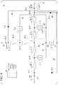
- FIG. 1 is a configuration diagram of a DC current breaking device according to the first embodiment.
- the DC current breaking device 1 illustrated in FIG. 1 includes mechanical disconnectors 2-1 to 2-3, current transformers 3-1 to 3-3, a semiconductor circuit breaker (S) 4, rectifying devices (rectifying devices) 5-1 to 5-3, commutation devices (C) 7-1 to 7-3, and a control unit 9.
- the mechanical disconnectors 2-1 to 2-3 are examples of mechanical contact type current disconnectors.
- a DC power transmission circuit to which the DC current breaking device 1 is applied includes DC power transmission lines 11 to 13, and a connection point j (a first connection point) to which the DC power transmission lines 11 to 13 are electrically connected.
- the DC power transmission lines 11 to 13 are respectively associated with three systems and are electrically connected to each other at the connection point j.
- the DC power transmission line 11 is an example of a first DC power transmission line
- the DC power transmission line 12 is an example of a second DC power transmission line
- the DC power transmission line 13 is an example of a third DC power transmission line.
- ends of the DC power transmission lines 11 to 13 not illustrated in FIG. 1 are connected to different connection destinations (not illustrated).
- the DC power transmission lines 11 to 13 are associated with, for example, a positive electrode of the DC power transmission circuit.
- description of the negative electrode side of the DC power transmission circuit may be omitted as illustrated in FIG. 1 .
- the DC power transmission line 11 is provided with the mechanical disconnector 2-1
- the DC power transmission line 12 is provided with the mechanical disconnector 2-2
- the DC power transmission line 13 is provided with the mechanical disconnector 2-3.
- the DC power transmission line 2-1 is an example of a first mechanical disconnector
- the DC power transmission line 2-2 is an example of a second mechanical disconnector
- the DC power transmission line 2-3 is an example of a third mechanical disconnector.
- a position at which the mechanical disconnector 2-1 is disposed is an end of the DC power transmission line 11.
- the mechanical disconnectors 2-2 and 2-3 the similarly configured mechanical disconnectors 2-1 to 2-3 may be collectively referred to as a mechanical disconnector 2. The same applies to other configurations.
- the number of mechanical disconnectors 2 provided in the respective DC power transmission cables of the DC power transmission lines 11 to 13 is not limited to one for each DC power transmission line, and may be plural.
- the DC power transmission lines 11 to 13 may be respectively provided with mechanical contact type current disconnectors that are the same as the mechanical disconnector 2 at the other ends thereof.
- Such a mechanical disconnector 2 may be used as a line switch.
- a steady current flowing through the DC power transmission lines 11 to 13 and an abnormal current due to a ground fault, a short circuit, or the like are broken by the DC current breaking device 1 to be described below.
- the DC power transmission line 11 is provided with the current transformer 3-1 that detects a current flowing through the DC power transmission line 11.
- the DC power transmission line 12 is provided with the current transformer 3-2 that detects a current flowing through the DC power transmission line 12.
- the DC power transmission line 13 is provided with the current transformer 3-3 that detects a current flowing through the DC power transmission line 13.
- the current transformer 3-1 is disposed at a position relatively near a junction point j3-1 and in a direction away from the connection point j.
- a position of the current transformer 3-1 illustrated in FIG. 1 is a position in a direction away from the connection point j with respect to the junction point j3-1, and is an example.
- the current transformers 3-1 to 3-3 output detection results regarding current values of the detected currents or detection results indicating overcurrent states of the detected currents.
- the DC current breaking device 1 further includes a common auxiliary line 20, an auxiliary line 21 (a first auxiliary line), an auxiliary line 22 (a second auxiliary line), and an auxiliary line 23 (a third auxiliary line).
- the common auxiliary line 20 and the auxiliary lines 21 to 23 are not provided with at least a mechanical contact type current disconnector, such as the mechanical disconnector 2.
- a first end of the auxiliary line 21 is electrically connected to a junction point j3-1 (a first position) located on the side opposite to the connection point j with respect to the mechanical disconnector 2-1 in the DC power transmission line 11.
- a first end of the auxiliary line 22 is electrically connected to a junction point j3-2 (a second position) located on the side opposite to the connection point j with respect to the mechanical disconnector 2-2 in the DC power transmission line 12.
- a first end of the auxiliary line 23 is electrically connected to a junction point j3-3 (a third position) located on the side opposite to the connection point j with respect to the mechanical disconnector 2-3 in the DC power transmission line 13.
- a second end of the auxiliary line 21, a second end of the auxiliary line 22, and a second end of the auxiliary line 23 are electrically connected to a connection point j2 (a second connection point).
- the common auxiliary line 20 electrically connects the connection point j to the connection point j2.
- the common auxiliary line 20 is provided with the semiconductor circuit breaker 4.
- the semiconductor circuit breaker 4 is an example of a first unit. Details of the semiconductor circuit breaker 4 will be described below.
- Each of the auxiliary lines 21 to 23 is provided with at least a second unit.
- the commutation devices 7-1 to 7-3 may have the same configuration.
- the commutation device 7 is an example of the second unit.
- the auxiliary line 21 is provided with the rectifying device 5-1 and the commutation device 7-1
- the auxiliary line 22 is provided with the rectifying device 5-2 and the commutation device 7-2
- the auxiliary line 23 is provided with the rectifying device 5-3 and the commutation device 7-3.
- the rectifying device 5-1 is provided in the auxiliary line 21 in a direction allowing a current due to the commutation relevant to the DC power transmission line 11 to flow through the auxiliary line 21.
- the rectifying device 5-2 is provided in the auxiliary line 22 in a direction allowing a current due to commutation relevant to the DC power transmission line 12 to flow through the auxiliary line 22.
- the rectifying device 5-3 is provided in the auxiliary line 23 in a direction allowing a current due to commutation relevant to the DC power transmission line 13 to flow through the auxiliary line 23.
- the direction allowing the current due to the commutation relevant to the DC power transmission line 11 to flow is a direction that matches a direction in which the current commutated by the commutation device 7 flows, and is directed from the connection point j2 to the junction point j3-1 in the auxiliary line 21.
- the rectifying device 5-1 causes a forward current to flow in that direction. The same applies to the rectifying device 5-2 and the rectifying device 5-3.
- the commutation device 7-1 operates so that a current flowing through the DC power transmission line 11 flows through the semiconductor circuit breaker 4 when a predetermined condition has been satisfied.
- the commutation device 7-2 operates so that a current flowing through the DC power transmission line 12 flows through the semiconductor circuit breaker 4 when the predetermined condition is satisfied.
- the commutation device 7-3 operates so that a current flowing through the DC power transmission line 13 flows through the semiconductor circuit breaker 4 when the predetermined condition is satisfied.
- the predetermined condition is what a current value of a current detected by any of the current transformers 3-1 to 3-3 exceeds a predetermined threshold value.
- the commutation device in which the predetermined condition has been satisfied among the commutation devices 7-1 to 7-3 commutates a current as described above. Details of the commutation device 7 will be described below.
- the rectifying device 5 may not be provided.
- the control unit 9 controls each unit of the DC current breaking device 1 on the basis of detection results of the respective current transformers 3-1 to 3-3. For example, the control unit 9 controls respective states of the mechanical disconnectors 2-1 to 2-3, the first unit, and the second unit such that the states are brought into an OFF state in which a current is blocked and an ON state in which the current flows.
- the first unit in the first embodiment is the semiconductor circuit breaker 4.
- the second unit in the first embodiment is the commutation device 7.
- FIGS.2A and 2B are diagrams illustrating a configuration example of the semiconductor circuit breaker in the first embodiment.
- a semiconductor circuit breaker 4A illustrated in FIG. 2A is an example of the semiconductor circuit breaker 4.
- the semiconductor circuit breaker 4A includes parallel circuit units 4U having the number of stages allowing a necessary withstand voltage to be exceeded. For example, a plurality of parallel circuit units 4U are connected in series.
- the parallel circuit unit 4U includes a semiconductor switching device 41 and an arrester 40. The semiconductor switching device 41 and the arrester 40 are connected in parallel to each other.
- a semiconductor circuit breaker 4B illustrated in FIG. 2B is an example of the semiconductor circuit breaker 4.
- the semiconductor circuit breaker 4B includes a semiconductor switching device array 41S in which semiconductor switching devices 41 having the number of stages allowing a necessary withstand voltage to be exceeded are connected in series, and an arrester 40.
- the arrester 40 is connected in parallel to the entire semiconductor switching device array 41S.
- the semiconductor circuit breakers 4A and 4B include at least a set of a plurality of semiconductor switching devices 41, and the arrester 40 connected in parallel to any one of the plurality of semiconductor switching devices 41 in the set.
- the semiconductor circuit breakers 4A and 4B include the plurality of semiconductor switching devices 41 connected in series.
- each of the semiconductor switching devices 41 of the semiconductor circuit breakers 4A and 4B includes an insulated gate bipolar transistor (IGBT) 41a and a rectifier 41b connected in parallel.
- IGBT 41a insulated gate bipolar transistor
- the IGBT 41a may be an injection enhanced gate transistor (IEGT).
- the semiconductor circuit breakers 4A and 4B may include at least one semiconductor switching device 41.
- the rectifier 41b is an example of a rectifying device.
- the plurality of semiconductor switching devices 41 connected in series are arranged with directions of polarities thereof uniformly aligned.
- the emitter of the IGBT 41a of the k-th semiconductor switching device 41 and the collector of the IGBT 41a of the (k+1)-th semiconductor switching device 41, which have been connected in series, are connected to each other, and this connection is repeated in order.
- the collector of the first semiconductor switching device 41 (the IGBT 41a) located at an end among the semiconductor switching devices 41 connected in series is connected to the connection point j in FIG. 1 .
- the anode of the rectifier 41b of the k-th semiconductor switching device 41 and the cathode of the rectifier 41b of the (k+1)-th semiconductor switching device 41, which have been connected in series, are connected to each other, and this connection is repeated in order.
- the cathode of the first rectifier 41b located at an end among the rectifiers 41b connected in series is connected to the connection point j in FIG. 1 .
- the semiconductor circuit breakers 4A and 4B when the IGBT 41a is caused to enter an OFF state so that the rectifier 41b enters a reverse bias state, the semiconductor circuit breakers 4A and 4B are in the broken state, and when the IGBT 41a is caused to turn to an ON state, the semiconductor circuit breaker 4A and 4B enter a conduction state.
- the semiconductor circuit breaker 4 includes at least one semiconductor switching device 41 and the arrester 40 connected in parallel to the at least one semiconductor switching device 41.
- the semiconductor circuit breaker 4 may be any one of the semiconductor circuit breakers 4A and 4B, or may be a semiconductor circuit breaker in another form.
- a plurality of semiconductor switching device arrays 41S illustrated in FIG. 2B may be connected in parallel to each other. That is, in the semiconductor circuit breaker 4, the plurality of semiconductor switching devices 41 may be connected in parallel. In this case, directions of the polarities of the plurality of semiconductor switching devices 41 are uniformly aligned.
- the semiconductor circuit breakers 4 according to an arrangement scheme described above may be a semiconductor circuit breaker in which directions of polarities of the semiconductor switching devices 41 connected in series or in parallel are aligned in the same direction and are directed in one specific direction only.
- FIGS. 3A to 3C are diagrams illustrating a configuration example of the commutation device in the first embodiment.
- An example of a commutation device 7 illustrated in FIGS. 3A to 3C includes one semiconductor switching device 72 or a plurality of semiconductor switching devices connected in series or in parallel.
- the semiconductor switching device 72 is included in the plurality of semiconductor switching devices.
- a semiconductor switching device such as the semiconductor switching device 72 is, for example, an IGBT or an IEGT. Next, a more specific example is shown.
- a commutation device 7A illustrated in FIG. 3A is an example of the commutation device 7.
- the commutation device 7A includes a capacitor 71, a leg 701, and a leg 702.
- Each of the leg 701 and the leg 702 includes one or more semiconductor switching devices 72 and one or more rectifiers 73.
- one semiconductor switching device 72 and one rectifier 73 are connected in series.
- the commutation device 7A includes at least one capacitor 71, two semiconductor switching devices 72, and two rectifiers 73.
- the rectifier 73 is an example of a rectifying device.
- a half bridge unit in which the leg 701, the leg 702, and the at least one capacitor 71 are disposed between a connection point j73 and a connection point j74 and connected in parallel to each other is formed.
- Each of connection points j71 and j72 between the semiconductor switching device 72 and the rectifier 73 in the leg 701 and the leg 702 is connected to the outside of the half bridge unit.
- the connection point j71 is electrically connected to the connection point j3 ( FIG. 1 ).
- the connection point j72 is electrically connected to the connection point j2 ( FIG. 1 ).
- Such a commutation device 7A is said to be a bridge type.
- the semiconductor switching device 72 includes, for example, one IGBT 72a and one rectifier 72b connected in parallel. In each semiconductor switching device 72, an emitter of the IGBT 72a is connected to an anode of the rectifier 72b, and a collector of the IGBT 72a is connected to a cathode of the rectifier 72b.
- the IGBT 72a may be an IEGT.
- the capacitor 71 is charged by a charging means (not illustrated) so that a potential at the connection point j73 is higher than a potential at the connection point j74.
- a charging means not illustrated
- the capacitor 71 is connected to the outside of the half-bridge unit and can be discharged.
- a commutation device 7B illustrated in FIG. 3B is an example of the commutation device 7.
- the commutation device 7B includes a capacitor 71 and a semiconductor switching device 72.
- the capacitor 71 and a collector of the semiconductor switching device 72 are connected in series at a connection point j75.
- Each of a connection point j71 of the semiconductor switching devices 72 and a connection point j72 of the capacitor 71 connected in series is connected to the outside of the commutation device 7.
- the connection point j71 of the semiconductor switching device 72 is connected to the connection point j3 ( FIG. 1 ), and the connection point j72 of the capacitor 71 is connected to the connection point j2 ( FIG. 1 ).
- the capacitor 71 is charged by a charging means (not illustrated) so that a potential on the connection point j75 side becomes higher than the potential on the connection point j72 side.
- a commutation device 7C illustrated in FIG. 3C is an example of the commutation device 7.
- the commutation device 7C includes a leg 703, a leg 704, and at least one capacitor 71.
- the leg 703 and the leg 704 are examples of a leg in which two or more switching elements are connected in series.
- One or more legs 703 or one or more legs 704 may be included, and when there are two or more legs 703 or two or more legs 704, the legs 703 or the legs 704 may be connected in parallel.
- the commutation device 7C includes a full bridge unit in which the leg 703, the leg 704, and the at least one capacitor 71 are disposed between a connection point j73 and a connection point j74 and connected in parallel to each other.
- the leg 703 includes one or more semiconductor switching devices 72 and one or more semiconductor switching devices 75.
- one semiconductor switching device 72 and one semiconductor switching device 75 are connected in series.
- the semiconductor switching device 72 and the semiconductor switching device 75 in the leg 703 are defined as the connection point j72.
- the semiconductor switching device 72 and the semiconductor switching device 74 in the leg 704 are defined as the connection point j71.
- each of the connection points j71 and j72 is connected to the outside of the full bridge unit.
- the connection point j72 of the leg 704 is electrically connected to the connection point j2 ( FIG. 1 )
- the connection point j71 of the leg 703 is electrically connected to the connection point j3 ( FIG. 1 ).
- Such a commutation device 7C is said to be a full bridge type.
- the semiconductor switching devices 72, 74, and 75 are of the same type.
- the semiconductor switching device 72 includes an IGBT 72a and a rectifier 72b connected in parallel.
- an emitter of the IGBT 72a is connected to an anode of the rectifier 72b, and a collector of the IGBT 72a is connected to a cathode of the rectifier 72b.
- the IGBT 72a may be an IEGT.
- the commutation device 7C may be caused to function as a half bridge type by using some of the semiconductor switching devices.
- the commutation device 7C may set the semiconductor switching devices 72 as a target of control for switching a conduction state of the IGBT 72a and keep respective IGBTs of the semiconductor switching devices 74 and 75 in an OFF state so that a rectifier may be used.
- the commutation device 7C may include one of the leg 703 and the leg 704 and the capacitor 71.
- the capacitor 71 may be charged using the same method as in the commutation device 74A.
- the capacitor 71 is charged to a desired DC voltage with a desired polarity in an operation of the DC power transmission circuit.
- the commutation device 7 causes a potential at the connection point j71 to be higher than a potential at the connection point j72 so that the commutation can be started.
- the configuration diagram of FIG. 1 or the like described above shows that the commutation device 7 has been charged so that the terminal of the commutation device 7 has a higher potential than the other terminal, by attaching a mark "+" near the terminal of the commutation device 7. The same applies to the following description.
- the commutation device 7 illustrated in each of FIGS. 3A to 3C has a configuration for one stage, but a configuration in which the commutation devices 7 are connected in series in a plurality of stages may be adopted.
- control unit 9 performs control so that the mechanical disconnectors 2-1 to 2-3 enter an ON state and the semiconductor circuit breaker 4 (the first unit) and all the commutation devices 7 (the second units) enter an OFF state.
- Current flowing through the DC power transmission lines 11 to 13 flows through the respective mechanical disconnectors 2-1 to 2-3.
- the control unit 9 breaks a current flowing through at least one DC power transmission line in which the system fault has occurred, according to the following procedure. Description will be given herein assuming that the system fault has occurred in the DC power transmission line 12 as illustrated in FIG. 1 . A fault current I A flows due to the above system fault.
- control unit 9 detects that the system fault has occurred, on the basis of a detection result of the fault current I A detected by the current transformer 3-2.
- the control unit 9 When the control unit 9 detects the system fault, the control unit 9 causes the semiconductor circuit breaker 4 to turn to the ON state, and causes the commutation device 7-2 corresponding to the DC power transmission line 12 in which the system fault has occurred, to turn to an operable state (an ON state). Thereby, a closed circuit CC1 including the commutation device 7-2, the rectifying device 5-2, the mechanical disconnector 2-2, and the semiconductor circuit breaker 4 through the connection points j and j2 is formed. When a current Icc flows through the closed circuit CC1 passing through the connection points j, j2, and j3-2, the fault current I A flowing through the mechanical disconnector 2-2 is canceled out and a substantially zero current state is caused.
- the mechanical disconnector 2-2 belonging to the DC power transmission line 12 in which the system fault has occurred is present in the closed circuit CC1 including the commutation device 7-2.
- the fault current I A flowing through the mechanical disconnector 2-2 is commutated to the commutation device 7-2, and the current Ic flows.
- the mechanical disconnector 2-2 can be caused to turn to the OFF state.
- control unit 9 causes the mechanical disconnector 2-2 in the zero current state to turn to the OFF state, and then causes the semiconductor circuit breaker 4 to enter the OFF state.
- the semiconductor circuit breaker 4 By causing the semiconductor circuit breaker 4 to enter the OFF state, energy generated at both ends of the semiconductor circuit breaker 4 is consumed by the arrester 40.
- the control unit 9 stops the operation of the commutation device 7-2 after the control unit 9 causes the mechanical disconnector 2-2 to turn to the OFF state.
- the DC current breaking device 1 can break the current flowing through the DC power transmission line 12 in which the system fault has occurred.
- the above operation is the same for the other DC power transmission lines.
- the number of the semiconductor circuit breakers 4 is one, and the semiconductor circuit breaker 4 is shared by the respective DC power transmission cables.
- the DC power transmission cable in which the system fault has occurred can be disconnected by one semiconductor circuit breaker 4.
- a DC current breaking device CE of a comparative example In order to break only one DC power transmission line in which a fault has occurred among a plurality of DC power transmission lines of a power transmission network (a DC power transmission circuit), it is necessary for a DC current breaking device CE of a comparative example to be provided at both ends of the DC power transmission line of the power transmission network (the DC power transmission circuit), with the DC power transmission line interposed therebetween, when the DC current breaking device CE of the comparative example is used.
- the number of DC current breaking devices CE increases when the number of DC power transmission lines is large.
- the DC current breaking device CE of the comparative example cannot be simply configured when the number of DC power transmission lines is large.
- the DC current breaking device 1 of the first embodiment one semiconductor circuit breaker 4 is shared among the DC power transmission lines 11 to 13. Thereby, it is not necessary to increase the number of the semiconductor circuit breakers 4 with an increase in the number of systems of DC power transmission lines.
- the DC current breaking device 1 of the first embodiment can be configured more simply as compared with the above comparative example, and the superiority of the DC current breaking device 1 is enhanced as the number of systems of applied DC power transmission lines increases.
- the first embodiment it is possible to reduce the number of semiconductor circuit breakers 4 as compared with the comparative example in which the DC current breaking device CE is individually connected to each of the DC power transmission lines 11 to 13, and thus, it is possible to reduce the number of components of the semiconductor switching device and achieve a low cost and small size for the DC current breaking device 1.
- the number of semiconductor circuit breakers 4 that can be reduced through sharing of the semiconductor circuit breakers 4 is (n-1).
- the semiconductor circuit breaker 4 in which it is necessary for an insulation withstand voltage to be ensured includes a large number of components of built-in semiconductor switching devices and is generally expensive. Thus, an effect of cost and reduction in the DC current breaking device 1 in which the number of semiconductor circuit breakers 4 can be reduced is relatively large.
- the DC current breaking device 1 of the first embodiment has the above advantages over the comparative example, it is still possible to break a fault current of a system fault at high speed.
- a configuration of the first embodiment is an example, and the number of systems of DC power transmission lines connected to the connection point is not limited to the above example, and the DC current breaking device 1 can be applied to a connection point to which any number of systems of DC power transmission lines are connected, or to a case in which the connection points are mechanically separated and disposed.
- the DC current breaking device 1 can be applied to a connection point of two or four or more DC power transmission lines or two separately disposed connection points.
- a plurality of commutation devices 7 may be formed in series. Further, some or all of at least one or more commutation devices 7 may be configured as a full bridge type.
- the semiconductor circuit breaker 4 may be configured so that a polarity of the semiconductor switching device is bidirectional or unidirectional.
- the number of mechanical disconnectors 2-1 provided in the DC power transmission line 11 in FIG. 1 is one, but may be plural, or mechanical contact type current disconnectors provided in the DC power transmission line 11 may be connected in series and parallel.
- the DC current breaking device 1 is provided in the DC power transmission circuit in which at least the DC power transmission line 11 and the DC power transmission line 12 are electrically connected to each other at the connection point j.
- the DC current breaking device 1 includes the mechanical disconnector 2-1, the mechanical disconnector 2-2, the auxiliary line 21, the auxiliary line 22, the common auxiliary line 20, the first unit, and the second unit.
- the mechanical disconnector 2-1 is provided in the DC power transmission line 11.
- the mechanical disconnector 2-1 is provided in the DC power transmission line 12.
- the auxiliary line 21 is electrically connected to the junction point j3-1 located on the side opposite to the connection point j with respect to the mechanical disconnector 2-1 in the DC power transmission line 11.
- the auxiliary line 22 is electrically connected to the junction point j3-2 located on the side opposite to the connection point j with respect to the mechanical disconnector 2-2 in the DC power transmission line 12.
- the common auxiliary line 20 is electrically connected between the connection point j2 to which the auxiliary line 21 and the auxiliary line 22 are electrically connected, and the connection point j.
- the first unit is provided in the common auxiliary line 20.
- the second unit is provided in each of a first line that is the DC power transmission line 11 or the auxiliary line 21, and a second line that is the DC power transmission line 12 or the auxiliary line 22.
- One of the first unit and the second unit is the semiconductor circuit breaker 4 that includes at least one semiconductor switching device and is capable of breaking a current.
- the other of the first unit and the second unit is the commutation device 7 that commutates the current flowing through the DC power transmission line 11 or the DC power transmission line 12 so that the current flows through the semiconductor circuit breaker 4 when a predetermined condition has been satisfied.
- the DC current breaking device 1 for breaking a fault current flowing through any of the DC power transmission cables at the connection point of the plurality of DC power transmission cables.
- the DC power transmission circuit includes the DC power transmission line 13 electrically connected to the connection point j.
- the DC current breaking device 1 further includes the mechanical disconnector 2-3 provided in the DC power transmission line 13, and the auxiliary line 23 electrically connected to the junction point j3-3 located on the side opposite to the connection point j with respect to the mechanical disconnector 2-3 in the DC power transmission line 13.
- the second unit is also provided on a third line which is the DC power transmission line 13 or the auxiliary line 23.
- the semiconductor circuit breaker 4 is enabled to break the current of each DC power transmission line. Thereby, it is possible to reduce the number of semiconductor circuit breakers 4 as compared with a case in which the semiconductor circuit breakers 4 are provided independently.
- the commutation device 7 can commutate a current to each DC power transmission line by being provided in each of the auxiliary line 21 and the auxiliary line 22.
- the rectifying device 5-1 is provided in the auxiliary line 21, and is provided in a direction allowing the current commutated by the commutation device 7 from the DC power transmission line 11 to flow.
- the rectifying device 5-2 is provided in the auxiliary line 21 and is provided in a direction allowing a current due to the commutation relevant to the DC power transmission line 11 to flow. Accordingly, a current in a direction different from that of the commutation can be limited without the commutation being limited.
- the commutation device 7 includes one semiconductor switching device or a plurality of semiconductor switching devices connected in series or in parallel. Therefore, it is possible to control the start of the commutation through an operation of the semiconductor switching device.
- the commutation device 7 can be configured as a full bridge type including one full bridge unit or two or more full bridge units connected in series, and in the full bridge unit, two of the legs (703, 704) in which a plurality of semiconductor switching devices are connected in series and the legs (701, 702) in which one or more semiconductor switching devices and one or more rectifying devices are connected in series, and at least one capacitor are connected in parallel.
- the commutation device 7 can be configured as a bridge type including one half bridge unit or two or more half bridge units connected in series, and in the half bridge unit, one of a leg in which a plurality of semiconductor switching devices are connected in series and a leg in which at least one semiconductor switching device and at least one rectifying device are connected in series, and at least one capacitor are connected in parallel.
- control unit 9 controls respective states of the mechanical disconnector 2, the first unit, and the second unit such that the states are brought into an OFF state in which the current is blocked and an ON state in which the current flows. In a steady operation until a system fault occurs in the DC power transmission line 11 or the DC power transmission line 12, the control unit 9 performs control so that the mechanical disconnector 2-1 or 2-2 enters the ON state and the unit and the second unit enter the OFF state.
- the control unit 9 causes the first unit, and the second unit corresponding to the DC power transmission line in which the system fault has occurred among the DC power transmission line 11 and the DC power transmission line 12 to turn to the ON state, so that a substantially zero current state is created for a current flowing through the mechanical disconnector 2 belonging to the DC power transmission line in which the system fault has occurred, which is any one mechanical disconnector 2 among the mechanical disconnectors 2-1 to 2-3, causes the mechanical disconnector 2 in the substantially zero current state to turn to the OFF state, and then causes the first unit, and the second unit corresponding to the DC power transmission line in which the system fault has occurred to enter the OFF state.
- breaking of the current flowing through the DC power transmission line in which the system fault has occurred with a simpler configuration.
- the DC power transmission circuit of the first embodiment can be configured without a semiconductor device such as the semiconductor circuit breaker 4 or the commutation device 7 being provided in the DC power transmission lines 11 to 13. With such a configuration, a conduction loss due to the semiconductor device does not occur in a steady operation. Further, such an effect becomes more significant when a relatively high current flows in a steady operation in the DC power transmission circuit.
- the mechanical disconnectors 2-1 to 2-3 of the first embodiment may not include the arresters connected in parallel.
- FIG. 4 is a configuration diagram of the DC current breaking device according to the second embodiment. Differences from FIG. 1 will be mainly described.
- a DC current breaking device 1 illustrated in FIG. 4 includes mechanical disconnectors 2-1 to 2-3, current transformers 3-1 to 3-3, semiconductor circuit breakers 4-1 to 4-3, a rectifying device 5, a commutation device 7, and a control unit 9.
- a DC power transmission circuit to which the DC current breaking device 1 is applied includes DC power transmission lines 11 to 13, and a connection point j2 (a first connection point) to which the DC power transmission lines 11 to 13 are electrically connected.
- the DC current breaking device 1 further includes a common auxiliary line 20, an auxiliary line 21 (a first auxiliary line), an auxiliary line 22 (a second auxiliary line), and an auxiliary line 23 (a third auxiliary line).
- auxiliary line 21 is electrically connected to a junction point j3-1 (a first position) located on the side opposite to the connection point j2 with respect to the mechanical disconnector 2-1 in the DC power transmission line 11.
- junction point j3-1 a first position located on the side opposite to the connection point j2 with respect to the mechanical disconnector 2-1 in the DC power transmission line 11.
- a second end of the auxiliary line 21, a second end of the auxiliary line 22, and a second end of the auxiliary line 23 are electrically connected to a connection point j (a second connection point).
- the common auxiliary line 20 is electrically connected between the connection point j and the connection point j2.
- the common auxiliary line 20 is provided with a rectifying device 5 and the commutation device 7.
- the commutation device 7 is an example of a first unit.
- the auxiliary line 21 is provided with the semiconductor circuit breaker 4-1
- the auxiliary line 22 is provided with the semiconductor circuit breaker 4-2
- the auxiliary line 23 is provided with the semiconductor circuit breaker 4-3.
- the semiconductor circuit breakers 4-1 to 4-3 are examples of a second unit. That is, the second unit is provided in at least each of the auxiliary line 21 and the auxiliary line 22. Further, the second unit is also provided on the auxiliary line 23. Thus, the second unit may be provided on each of the auxiliary lines.
- the rectifying device 5 is provided in the common auxiliary line 20 together with the commutation device 7 so that the rectifying device 5 is electrically in series with the commutation device 7.
- the rectifying device 5 is provided in a direction allowing a current due to commutation relevant to any of the DC power transmission lines 11 to 13 to flow through the common auxiliary line 20.
- the commutation device 7 operates so that a current flowing through the DC power transmission line 11 flows through any one of the semiconductor circuit breakers 4-1 to 4-3 when a predetermined condition has been satisfied.
- the direction allowing the current due to the commutation relevant to the DC power transmission line 11 to flow is a direction from the connection point j2 to the connection point j in the common auxiliary line 20.
- the rectifying device 5 causes a forward current to flow in that direction.
- the control unit 9 When the control unit 9 detects the system fault, the control unit 9 causes the semiconductor circuit breaker 4-2 to turn to the ON state, and causes the commutation device 7 corresponding to the DC power transmission line 12 in which the system fault has occurred, to turn to an operable state (an ON state). Thereby, a closed circuit including the commutation device 7, the rectifying device 5, the semiconductor circuit breaker 4-2, and the mechanical disconnector 2-2 through the connection points j and j2 is formed. When a current Icc flows through the closed circuit passing through the connection points j, j2, and j3-2, the fault current I A flowing through the mechanical disconnector 2-2 is canceled out and a substantially zero current state is caused.
- the substantially zero current state includes a state in which a combined current of the current Icc and the fault current I A becomes zero (a zero current state).
- the fault current I A flowing through the mechanical disconnector 2-2 is commutated to the commutation device 7-2, and a current Ic flows.
- control unit 9 causes the mechanical disconnector 2-2 in the zero current state to turn to the OFF state, and then causes the semiconductor circuit breaker 4-2 to enter the OFF state.
- the semiconductor circuit breaker 4-2 By causing the semiconductor circuit breaker 4-2 to enter the OFF state, energy generated at both ends of the semiconductor circuit breaker 4-2 is consumed by the arrester 40.
- the control unit 9 stops the operation of the commutation device 7 after the control unit 9 causes the mechanical disconnector 2-2 in the zero current state to turn to the OFF state.
- the DC current breaking device 1 can break the current flowing through the DC power transmission line 12 in which the system fault has occurred.
- the above operation is the same for the other DC power transmission cables.
- the number of commutation devices 7 is one, and the commutation device 7 is shared by the respective DC power transmission cables. Thus, even when the system fault occurs in the DC power transmission cable of any one of the DC power transmission lines 11 to 13, the one commutation device 7 can operate to disconnect the DC power transmission cable in which the system fault has occurred.
- the first unit is the commutation device 7
- the second unit is the semiconductor circuit breaker 4
- the semiconductor circuit breaker 4 is provided in each of the auxiliary line 21 and the auxiliary line 22, thereby enabling the commutation device 7 to be shared in order to break the current of each DC power transmission line, in addition to achievement of the same effects as in the first embodiment.
- the rectifying device 5 is provided electrically in series with the commutation device 7 (the first unit) in a direction allowing the current due to the commutation to flow, it is possible to limit a current in a direction different from that of the commutation without limiting the commutation.
- FIG. 5 is a configuration diagram of the DC current breaking device according to the third embodiment. Differences from FIG. 1 will be mainly described.
- the DC current breaking device 1 illustrated in FIG. 5 includes mechanical disconnectors 2-1 and 2-2, current transformers 3-1 and 3-2, a semiconductor circuit breaker 4, rectifying devices 5-1 and 5- 2, commutation devices 7-1 and 7-2, a control unit 9, and a converter 10.
- the converter 10 may be a device external to the DC current breaking device 1.
- a DC power transmission circuit to which the DC current breaking device 1 is applied includes DC power transmission lines 11, 12, and 14, and a connection point j (a first connection point) to which the DC power transmission lines 11, 12, and 14 are electrically connected.
- the DC current breaking device 1 further includes a common auxiliary line 20, an auxiliary line 21 (a first auxiliary line), and an auxiliary line 22 (a second auxiliary line).
- a DC power transmission line 14 is connected to a connection point j instead of the DC power transmission line 13 of the first embodiment.
- the DC power transmission line 14 has a first end connected to the connection point j (a first connection point), and a second end connected to a DC side terminal of the converter 10.
- a three-phase AC power transmission line 15 is connected to an AC side terminal of the converter 10, and a power generator (G) 10G is connected to the AC side terminal of the converter 10 via the three-phase AC power transmission line 15.
- the power generator 10G is a three-phase AC generator.
- FIG. 6 illustrates a configuration of the converter 10.
- FIG. 6 is a configuration diagram illustrating the converter according to the third embodiment.
- the converter 10 includes an AC-to-DC converter 10A, a transformer 10B, and an AC circuit breaker 10C.
- the AC-to-DC converter 10A performs bidirectional conversion between an AC power and a DC power.
- Such a converter 10 performs mutual conversion of power between a three-phase AC power transmission line 15 side terminal and a DC power transmission line 14 side terminal.
- the control unit 9 controls each unit of the DC current breaking device 1 on the basis of detection results of the current transformers 3-1 and 3-2.
- the control unit 9 may further control the converter 10 on the basis of the detection results of the current transformers 3-1 and 3-2.
- description of a connection between the control unit 9 and the converter 10 will be omitted.
- the DC power transmission circuit of the third embodiment corresponds to that of the first embodiment described above.
- the DC current breaking device 1 operates as in the first embodiment.
- the third embodiment it is possible to apply DC current breaking device to the DC power transmission circuit 14 in which the power generator 10G or the like is connected to the connection point j via the converter 10, in addition to achievement of the same effects as those of the first embodiment.
- the DC current breaking device is individually connected to each of the DC power transmission lines 11 and 12, while enhancing a degree of freedom of a configuration of the applicable DC power transmission circuit.
- FIG. 7 is a configuration diagram of the DC current breaking device according to the fourth embodiment. Differences from FIG. 1 will be mainly described.
- the DC current breaking device 1 illustrated in FIG. 7 includes mechanical disconnectors 2-1 to 2-3, current transformers 3-1 to 3-3, a semiconductor circuit breaker 4, rectifying devices 5-1 to 5- 3, commutation devices 7T-1 to 7T-3, and a control unit 9.
- a DC power transmission circuit to which the DC current breaking device 1 illustrated in FIG. 7 is applied includes DC power transmission lines 11 to 13, and a connection point j (a first connection point) to which the DC power transmission lines 11 to 13 are electrically connected to each other.
- the DC current breaking device 1 further includes a common auxiliary line 20, an auxiliary line 21 (a first auxiliary line), an auxiliary line 22 (a second auxiliary line), and an auxiliary line 23 (a third auxiliary line).
- the DC current breaking device 1 includes a first unit provided in the common auxiliary line 20.
- the DC current breaking device 1 includes a second unit provided in each of the DC power transmission line 11 (a first line), the DC power transmission line 12 (a second line), and the DC power transmission line 13 (a third line).
- the semiconductor circuit breaker 4 is an example of the first unit, and the commutation devices 7T-1 to 7T-3 are examples of the second unit.
- the DC power transmission line 11 is provided with the mechanical disconnector 2-1 and the commutation device 7T-1
- the DC power transmission line 12 is provided with the mechanical disconnector 2-2 and the commutation device 7T-2
- the DC power transmission line 13 is provided with the mechanical disconnector 2-3 and the commutation device 7T-3, as illustrated in FIG. 7 .
- the mechanical disconnector 2-1 is disposed at an end of the DC power transmission line 11
- the mechanical disconnector 2-2 is disposed at an end of the DC power transmission line 12
- the mechanical disconnector 2-3 is disposed at an end of the DC power transmission line 13.
- the number of mechanical disconnectors 2-1 to 2-3 respectively provided in the respective DC power transmission cables of the DC power transmission lines 11 to 13 is not limited to one, and may be plural.
- FIGS. 8A and 8B are diagrams illustrating a configuration example of the commutation device in the fourth embodiment.
- An example of a commutation device 7T illustrated in FIGS. 8A and 8B includes one semiconductor switching device 72 or a plurality of semiconductor switching devices connected in series or in parallel.
- the semiconductor switching device 72 is included in the plurality of semiconductor switching devices.
- a semiconductor switching device such as the semiconductor switching device 72 is, for example, an IGBT or an IEGT. Next, a more specific example is shown.
- a commutation device 7D illustrated in FIG. 8A is an example of the commutation device 7T.
- the commutation device 7D includes one semiconductor switching device 75.
- the semiconductor switching device 75 includes an IGBT 75a and a rectifier 75b connected in parallel.
- an emitter of the IGBT 75a is connected to an anode of the rectifier 75b, and a collector of the IGBT 75a is connected to a cathode of the rectifier 75b.
- the IGBT 75a may be an IEGT.
- Each of connection points j71 and j72 of the commutation device 7 is connected to the outside of the commutation device 7T.
- the connection point j71 is electrically connected to the mechanical disconnector 2-1 ( FIG. 7 ) or the like.
- the connection point j72 is electrically connected to the connection point j ( FIG. 7 ).
- a commutation device 7E illustrated in FIG. 8B is an example of the commutation device 7T.
- the commutation device 7E includes a leg 703, a leg 704, and at least one capacitor 71.
- the commutation device 7E has the same configuration as the commutation device 7C described above. However, the commutation device 7E is different from that of the commutation device 7C in a connection destination.
- a semiconductor switching device 72 and a semiconductor switching device 75 in the leg 703 are defined as the connection point j71.
- a semiconductor switching device 72 and a semiconductor switching device 74 in the leg 704 are defined as the connection point j72.
- each of the connection points j71 and j72 is connected to the outside of a full bridge unit.
- the connection point j72 of the leg 704 is electrically connected to the connection point j ( FIG. 7 )
- the connection point j72 of the leg 703 is electrically connected to the mechanical disconnector 2 ( FIG. 7 ) or the like.
- Such a commutation device 7E is said to be a full bridge type.
- the control unit 9 performs control so that the mechanical disconnectors 2-1 to 2-3 and all the commutation devices 7T (a second unit) enter an ON state and the semiconductor circuit breaker 4 (a first unit) enters an OFF state.
- a current flowing through the DC power transmission line 11 flows through the mechanical disconnector 2-1 and the commutation device 7T-1.
- a current flowing through the DC power transmission line 12 flows through the mechanical disconnector 2-2 and the commutation device 7T-2.
- a current flowing through the DC power transmission line 13 flows through the mechanical disconnector 2-3 and the commutation device 7T-3.
- the control unit 9 breaks a current flowing through at least one DC power transmission line in which the system fault has occurred, according to the following procedure. Description will be given herein assuming that the system fault has occurred in the DC power transmission line 12 as illustrated in FIG. 1 . A fault current I A flows due to the above system fault.
- control unit 9 detects that the system fault has occurred, on the basis of a detection result of the fault current I A detected by the current transformer 3-2.
- control unit 9 When the control unit 9 detects the system fault, the control unit 9 causes the semiconductor circuit breaker 4 to turn to the ON state, and operates the commutation device 7T-2 corresponding to the DC power transmission line 12 in which the system fault has occurred, so that the commutation device 7T-2 enters an OFF state or a current flowing therethrough is zero.
- the commutation device 7T-2 when the commutation device 7T-2 is caused to enter the OFF state, commutation to a path passing through the connection points j and j2 occurs, the current 1c flows, and a substantially zero current state of the fault current 1a flowing through the mechanical disconnector 2-2 is created.
- the commutation device 7T-2 when the commutation device 7T-2 is operated so that the current flowing through the commutation device 7T-2 becomes zero, the commutation device 7T-2 causes, for example, the current Icc to flow through a closed circuit including the commutation device 7-2, the semiconductor circuit breaker 4, the rectifying device 5-2, and the mechanical disconnector 2-2 through the connection points j and j2.
- the current Icc flows through the closed circuit passing through the connection points j and j2
- the fault current I A flowing through the mechanical disconnector 2-2 is canceled out and a substantially zero current state is caused.
- the fault current I A flowing through the mechanical disconnector 2-2 is commutated to the semiconductor circuit breaker 4, and the current Ic flows.
- the mechanical disconnector 2-2 can be caused to turn to the OFF state.
- control unit 9 causes the mechanical disconnector 2-2 in the zero current state to turn to the OFF state, and then causes the semiconductor circuit breaker 4 to enter the OFF state.
- the semiconductor circuit breaker 4 By causing the semiconductor circuit breaker 4 to enter the OFF state, energy generated at both ends of the semiconductor circuit breaker 4 is consumed by the arrester 40.
- the control unit 9 may cause the commutation device 7-2 to turn to an OFF state or a state in which an operation has been stopped, after the fault current I A is commutated to the semiconductor circuit breaker 4.
- the DC current breaking device 1 can break the current flowing through the DC power transmission line 12 in which the system fault has occurred.
- the DC current breaking device 1 can break the current flowing through the DC power transmission line 11 or the DC power transmission line 12 in the DC power transmission circuit in which the commutation device 7T-1 is provided in the DC power transmission line 11 and he commutation device 7T-2 is provided in the DC power transmission line 12, in addition to achievement of the same effects as in the first embodiment.
- the DC current breaking device 1 can break the current flowing through the DC power transmission line 13 in the DC power transmission circuit in which the commutation device 7T-3 is provided in the DC power transmission line 13.
- a section Sec1 illustrated in FIG. 7 is an example of the first section
- a section Sec2 is an example of the second section
- a section Sec3 is an example of the third section.
- the rectifying device 5-1 is provided in the auxiliary line 21, and is provided in a direction allowing the current commutated by the commutation device 7 from the DC power transmission line 11 to flow.
- the rectifying device 5-2 is provided in the auxiliary line 22 and is provided in a direction allowing the current commutated by the commutation device 7 from the DC power transmission line 11 to flow. Accordingly, a current in a direction different from that of the commutation can be limited without the commutation being limited.
- the commutation device 7T has a function of commutating the current flowing through each DC power transmission cable to the semiconductor circuit breaker 4, and is configured so that at least a rated current flows continuously.
- a configuration of such a commutation device 7T is not limited to the configuration illustrated in FIG. 8A .
- the semiconductor switching device 75 of the commutation device 7D illustrated in FIG. 8A can control a unidirectional current conduction state, but can control a bidirectional current conduction state.
- the semiconductor circuit breaker 4 may be capable of controlling a unidirectional current conduction state or may be capable of controlling a bidirectional current conduction state in the semiconductor switching device 41. Such a semiconductor circuit breaker 4 may have either a bidirectional conduction state or an only unidirectional current conduction state.
- control unit 9 controls respective states of the mechanical disconnector 2, the semiconductor circuit breaker 4, and the commutation device 7T such that the states are brought into an OFF state in which the current is blocked and an ON state in which the current flows.
- the control unit 9 operates the mechanical disconnector 2 and the commutation device 7T such that the mechanical disconnector 2 and the commutation device 7T are brought into an ON state and the semiconductor circuit breaker 4 such that the semiconductor circuit breaker 4 is brought into an OFF state.
- the control unit 9 causes the semiconductor circuit breaker 4 to turn to an ON state, thereby commutating the current to the semiconductor circuit breaker 4.
- control unit 9 causes the mechanical disconnector 2-1 or 2-2 in a substantially zero current state to turn to an OFF state and causes the semiconductor circuit breaker 4 to enter an OFF state. Thereby, it is possible to start the commutation by causing the commutation device 7T-1 or 7T-2 disposed so that the current of the DC power transmission line 11 or the DC power transmission line 12 flows in the steady operation to enter the OFF state.
- FIG. 9 is a configuration diagram of the DC current breaking device according to the fifth embodiment. Differences from FIG. 1 will be mainly described.
- a DC current breaking device 1 illustrated in FIG. 9 includes mechanical disconnectors 2-1 to 2-3, mechanical disconnectors 2A-1 to 2A-3, current transformers 3-1 to 3-3, a semiconductor circuit breaker 4, rectifying devices 5-1 to 5-3, commutation devices 7-1 to 7-3, and a control unit 9.
- the mechanical disconnector 2A-1 is an example of a fourth mechanical disconnector
- the mechanical disconnector 2A-2 is an example of a fifth mechanical disconnector
- the mechanical disconnector 2A-3 is an example of a sixth mechanical disconnector.
- a DC power transmission circuit to which the DC current breaking device 1 is applied includes DC power transmission lines 11 to 13, and a connection point j (a first connection point) to which the DC power transmission lines 11 to 13 are electrically connected.
- the DC current breaking device 1 further includes a common auxiliary line 20, an auxiliary line 21 (a first auxiliary line), an auxiliary line 22 (a second auxiliary line), an auxiliary line 23 (a third auxiliary line), an auxiliary line 24 (a fourth auxiliary line), an auxiliary line 25 (a fifth auxiliary line), and an auxiliary line 26 (a sixth auxiliary line).
- a common auxiliary line 20 an auxiliary line 21 (a first auxiliary line), an auxiliary line 22 (a second auxiliary line), an auxiliary line 23 (a third auxiliary line), an auxiliary line 24 (a fourth auxiliary line), an auxiliary line 25 (a fifth auxiliary line), and an auxiliary line 26 (a sixth auxiliary line).
- the mechanical disconnector 2A-1 is provided on the side opposite to the connection point j with respect to the mechanical disconnector 2-1 in the DC power transmission line 11.
- the mechanical disconnector 2A-2 is provided on the side opposite to the connection point j with respect to the mechanical disconnector 2-2 in the DC power transmission line 12.
- the mechanical disconnector 2A-3 is provided on the side opposite to the connection point j with respect to the mechanical disconnector 2-3 in the DC power transmission line 13.
- the mechanical disconnector 2 is a circuit breaker having a function of breaking a current
- the mechanical disconnector 2A is a disconnector having a high withstand voltage
- a first end of the auxiliary line 24 is electrically connected to a junction point j5-1 (a fourth position) located on the side opposite to the connection point j with respect to the mechanical disconnector 2A-1 in the DC power transmission line 11, and a connection point j2.
- a first end of the auxiliary line 25 is electrically connected to a junction point j5-2 (a fifth position) located on the side opposite to the connection point j with respect to the mechanical disconnector 2A-2 in the DC power transmission line 12, and the connection point j2.
- a first end of the auxiliary line 26 is electrically connected to a junction point j5-3 (a sixth position) located on the side opposite to the connection point j with respect to the mechanical disconnector 2A-3 in the DC power transmission line 13, and the connection point j2.
- a second end of the auxiliary line 24, a second end of the auxiliary line 25, and a second end of the auxiliary line 26 are electrically connected to the connection point j2 (the second connection point). That is, the auxiliary line 21 is provided between a junction point j3-1 located between the mechanical disconnector 2-1 and the mechanical disconnector 2A-1 in the DC power transmission line 11, and the connection point j2 and is electrically connected to the junction point j3-1 and the connection point j2.
- the rectifying device 5-1 is provided in the auxiliary line 24 in a direction allowing the current commutated by the commutation device 7 from the DC power transmission line 11 to flow through the auxiliary line 24.
- the rectifying device 5-2 is provided in the auxiliary line 25 in a direction allowing the current commutated by the commutation device 7 from the DC power transmission line 12 to flow through the auxiliary line 25.
- the rectifying device 5-3 is provided in the auxiliary line 26 in a direction allowing a current due to commutation relevant to the DC power transmission line 13 to flow through the auxiliary line 26.
- the rectifying device 5-1 is provided so that a forward current flows in a direction from the connection point j2 to the junction point j5. The same applies to the rectifying devices 5-2 and 5-3.
- the common auxiliary line 20 electrically connects the connection point j to the connection point j2.
- the common auxiliary line 20 is provided with the semiconductor circuit breaker 4.
- a position at which the semiconductor circuit breaker 4 is provided in the common auxiliary line 20 is between a junction point j4 and the connection point j2.
- the junction point j4 is disposed at a position at which the auxiliary lines 21 to 23 and the common auxiliary line 20 are electrically connected to each other.
- the control unit 9 performs control so that the mechanical disconnectors 2-1 to 2-3, the mechanical disconnectors 2A-1 to 2A-3 enter an ON state, and the semiconductor circuit breaker 4 (a first unit) and all the commutation devices 7 (second units) enter an OFF state. Currents flowing through the DC power transmission lines 11 to 13 are transmitted through the mechanical disconnector 2 and the mechanical disconnector 2A.
- the control unit 9 breaks a current flowing through at least one DC power transmission line in which the system fault has occurred, according to the following procedure. Description will be given herein assuming that the system fault has occurred in the DC power transmission line 12 as illustrated in FIG. 9 .
- a fault current I A flows through the mechanical disconnector 2-2 and the mechanical disconnector 2A-2 due to the above system fault.
- control unit 9 detects that the system fault has occurred, on the basis of a detection result of the fault current I A detected by the current transformer 3-2.
- control unit 9 When the control unit 9 detects the system fault, the control unit 9 causes the semiconductor circuit breaker 4 to turn to the ON state, and causes the commutation device 7-2 corresponding to the DC power transmission line 12 in which the system fault has occurred, to turn to an operable state (an ON state). Thereby, a closed circuit including the commutation device 7-2 and the mechanical disconnector 2-2 through the connection point j is formed. When a current Icc flows through the closed circuit passing through the connection point j, the fault current I A flowing through the mechanical disconnector 2-2 is canceled out and a substantially zero current state is caused.
- the mechanical disconnector 2-2 belonging to the DC power transmission line 12 in which the system fault has occurred is present in the closed circuit including the commutation device 7-2.
- the fault current I A flowing through the mechanical disconnector 2-2 is commutated to the semiconductor circuit breaker 4, and the current Ic passing through the rectifying device 5-2 flows.
- the mechanical disconnector 2-2 can be caused to turn to the OFF state.
- control unit 9 causes the mechanical disconnector 2-2 in the zero current state to turn to the OFF state. Further, the control unit 9 causes the mechanical disconnector 2A-2 in the zero current state to turn to the OFF state, and then causes the semiconductor circuit breaker 4 to enter the OFF state. By causing the semiconductor circuit breaker 4 to enter the OFF state, energy generated at both ends of the semiconductor circuit breaker 4 is consumed by the arrester 40.
- the control unit 9 may cause the commutation device 7-2 to turn to an OFF state after the fault current I A is commutated to the semiconductor circuit breaker 4.
- the DC current breaking device 1 can break the current flowing through the DC power transmission line 12 in which a system fault has occurred.
- the above operation is the same for the other DC power transmission cables.
- the number of the semiconductor circuit breakers 4 is one, and the semiconductor circuit breaker 4 is shared by the respective DC power transmission cables. Thus, even when the system fault has occurred in the DC power transmission cable of any one of the DC power transmission lines 11 to 13, the DC power transmission cable in which the system fault has occurred can be disconnected by one semiconductor circuit breaker 4.
- the mechanical disconnector 2A-1 is provided on the side opposite to the connection point j with respect to the mechanical disconnector 2-1 in the DC power transmission line 11, in addition to the achievement of the same effects as in the first embodiment.
- the mechanical disconnector 2A-2 is provided on the side opposite to the connection point j with respect to the mechanical disconnector 2-2 in the DC power transmission line 12.
- the auxiliary line 24 is electrically connected to the junction point j5-1 located on the side opposite to the connection point j1 with respect to the mechanical disconnector 2A-1 in the DC power transmission line 11, and the connection point j2.
- the auxiliary line 25 is electrically connected to the junction point j5-2 located on the side opposite to the connection point j with respect to the mechanical disconnector 2A-2 in the DC power transmission line 12, and the connection point j2.
- the fault current I ⁇ generated in the DC power transmission line 11 or the DC power transmission line 12 can be commutated to a path including the auxiliary line 24 or the auxiliary line 25.
- the semiconductor circuit breaker 4 can break a current due to the commutation relevant to the DC power transmission line 11 or the DC power transmission line 12.
- FIG. 10 is a configuration diagram of the DC current breaking device according to the sixth embodiment. Differences from FIGS. 1 and 9 will be mainly described.
- a DC current breaking device 1 illustrated in FIG. 10 includes mechanical disconnectors 2-1 to 2-3, mechanical disconnectors 2A-1 to 2A-3, current transformers 3-1 to 3-3, a semiconductor circuit breaker 4, rectifying devices 5-1 to 5-3, a rectifying device 5A, commutation devices 7-1 to 7-3, and a control unit 9.
- a first end of the auxiliary line 21 is electrically connected to a junction point j3-1 (a first position) located on the side opposite to the connection point j with respect to the mechanical disconnector 2A-1 in the DC power transmission line 11.
- a first end of the auxiliary line 22 is electrically connected to a junction point j3-2 (a second position) located on the side opposite to the connection point j with respect to the mechanical disconnector 2A-2 in the DC power transmission line 12.
- a first end of the auxiliary line 23 is electrically connected to a junction point j3-3 (a third position) located on the side opposite to the connection point j with respect to the mechanical disconnector 2A-3 in the DC power transmission line 13.
- At least a second end of the auxiliary line 21, a second end of the auxiliary line 22, and a second end of the auxiliary line 23 are electrically connected to a connection point j2 (a second connection point).
- auxiliary line 24 is electrically connected to a junction point j5-1 (a fourth position) located on the side opposite to the connection point j with respect to the mechanical disconnector 2-1 in the DC power transmission line 11, and a connection point j2.
- the auxiliary line 25 is electrically connected to a junction point j5-2 (a fifth position) located on the side opposite to the connection point j with respect to the mechanical disconnector 2-2 in the DC power transmission line 12, and the connection point j2.
- the auxiliary line 26 is electrically connected to a junction point j5-3 (a sixth position) located on the side opposite to the connection point j with respect to the mechanical disconnector 2-3 in the DC power transmission line 13, and the connection point j2.
- the mechanical disconnector 2-1 is provided on the side opposite to the connection point j with respect to the mechanical disconnector 2A-1 in the DC power transmission line 11.
- the mechanical disconnector 2-2 is provided on the side opposite to the connection point j with respect to the mechanical disconnector 2A-2 in the DC power transmission line 12.
- the mechanical disconnector 2-3 is provided on the side opposite to the connection point j with respect to the mechanical disconnector 2A-3 in the DC power transmission line 13.
- the mechanical disconnector 2A-1 is an example of a first mechanical disconnector
- the mechanical disconnector 2A-2 is an example of a second mechanical disconnector
- the mechanical disconnector 2A-3 is an example of a third mechanical disconnector.
- the mechanical disconnector 2-1 is an example of a fourth mechanical disconnector
- the mechanical disconnector 2-2 is an example of a fifth mechanical disconnector
- the mechanical disconnector 2-3 is an example of a sixth mechanical disconnector.
- a position at which the semiconductor circuit breaker 4 and the rectifying device 5A are provided in the common auxiliary line 20 is between the connection point j and the connection point j2.
- the connection point j2 is disposed at a position at which the auxiliary lines 21 to 26 and the common auxiliary line 20 are electrically connected to each other.
- the commutation devices 7A, 7B, and 7C illustrated in FIG. 3 described above can be applied.
- the commutation device 7 is provided such that the junction point j2 side has a higher potential than the junction point j3-2 side.
- the control unit 9 When the control unit 9 detects the system fault, the control unit 9 causes the semiconductor circuit breaker 4 to turn to the ON state, and causes the commutation device 7-2 corresponding to the DC power transmission line 12 in which the system fault has occurred, to turn to an operable state (an ON state). Thereby, a closed circuit including the commutation device 7-2, the rectifying device 5-2, and the mechanical disconnector 2-2A through the connection point j is formed. When a current Icc flows through the closed circuit passing through the connection point j, the fault current IA flowing through the mechanical disconnector 2-2 and the mechanical disconnector 2A-2 is canceled out and a substantially zero current state is caused.
- the mechanical disconnector 2-2 belonging to the DC power transmission line 12 in which the system fault has occurred is present in the closed circuit including the commutation device 7-2.
- the fault current IA flowing through the mechanical disconnector 2-2 is commutated to the semiconductor circuit breaker 4, and the current Ic passing through the rectifying device 5-2 flows.
- the mechanical disconnector 2-2 can be caused to turn to the OFF state.
- control unit 9 causes the mechanical disconnector 2-2 in the zero current state to turn to the OFF state. Further, the control unit 9 causes the mechanical disconnector 2A-2 in the zero current state to turn to the OFF state, and then causes the semiconductor circuit breaker 4 to enter the OFF state. By causing the semiconductor circuit breaker 4 to enter the OFF state, energy generated at both ends of the semiconductor circuit breaker 4 is consumed by the arrester 40.
- the control unit 9 causes the fault current IA to be commutated to the semiconductor circuit breaker 4, causes the mechanical disconnector 2-2 and the mechanical disconnector 2A-2 to turn to the OFF state, and then causes the commutation device 7-2 to turn to the OFF state.
- the DC current breaking device 1 can break the current flowing through the DC power transmission line 12 in which the system fault has occurred.
- the above operation is the same for the other DC power transmission cables.
- the mechanical disconnector 2A-1 is an example of the first mechanical disconnector
- the mechanical disconnector 2A-2 is an example of the second mechanical disconnector
- the mechanical disconnector 2-1 is an example of the fourth mechanical disconnector
- the mechanical disconnector 2-2 is an example of the fifth mechanical disconnector
- the first unit is the commutation device 7
- the second unit is the semiconductor circuit breaker 4
- the commutation device 7 can commutate the current relevant to the DC power transmission line 11 or the DC power transmission line 12, in addition to achievement of the same effects as in the first embodiment.
- FIG. 11 is a configuration diagram of the DC current breaking device according to the seventh embodiment. Differences from FIG. 10 will be mainly described.
- a DC current breaking device 1 illustrated in FIG. 11 includes mechanical disconnectors 2B-1 to 2B-3, mechanical disconnectors 2A-1 to 2A-3, current transformers 3-1 to 3-3, commutation devices (C) 7E-1 to 7E-3, a resonator (LC) 8, and a control unit 9.
- the DC current breaking device 1 of the sixth embodiment does not include the semiconductor circuit breaker (S) 4, the rectifying devices 5-1 to 5-3, the rectifying device 5A, and the auxiliary lines 24 to 26, and instead includes the resonator 8.
- the resonator 8 is an example of a resonance circuit. Further, types of the mechanical disconnector 2 and the commutation device 7 are different from each other.
- the common auxiliary line 20 is provided with the resonator 8, and the resonator 8 is connected between the connection points j and j2.
- FIG. 12 is a configuration diagram of the resonator 8 according to the seventh embodiment.
- the resonator 8 is an example of a series resonance circuit including a capacitor 81 and a reactor 82. Resonance occurs at a frequency determined by the capacitor 81 and the reactor 82.
- the auxiliary line 21 is provided with a commutation device 7E-1
- the auxiliary line 22 is provided with a commutation device 7E-2
- the auxiliary line 23 is provided with a commutation device 7E-3.
- the commutation devices 7E-1 to 7E-3 are configured as the full-bridge type commutation device 7E illustrated in FIG. 8B described above and configured to be able to output positive and negative voltages.
- the commutation devices 7E-1 to 7E-3 operate to increase current oscillation of the resonator 8.
- the mechanical disconnectors 2B-1 to 2B-3 are circuit breakers configured in the same structure and having a function of breaking a current.
- the mechanical disconnectors 2A-1 to 2A-3 are disconnectors configured in the same structure and having high withstand voltage characteristics.
- the control unit 9 When the control unit 9 detects the system fault, the control unit 9 causes the commutation device 7E-2 corresponding to the DC power transmission line 12 in which the system fault has occurred, to turn to an operable state (an ON state). Thereby, the commutation device 7E-2 can increase a resonance current of the resonator 8.
- a closed circuit including the resonator 8, the commutation device 7E-2, and the mechanical disconnector 2B-2 through the connection point j is formed.
- the mechanical disconnector 2B-2 belonging to the DC power transmission line 12 in which the system fault has occurred is present in the closed circuit including the commutation device 7E-2.
- the fault current IA flowing through the mechanical disconnector 2B-2 is limited by the commutation device 7E-2, and the current Ic passing through the commutation device 7E-2 flows.
- the mechanical disconnector 2B-2 enters a zero current state, the mechanical disconnector 2B-2 can be caused to turn to the OFF state.
- control unit 9 causes the mechanical disconnector 2B-2 to turn to the OFF state. Energy generated between electrical contacts of the mechanical disconnector 2B-2 by causing the mechanical disconnector 2B-2 to enter the OFF state is consumed by the arrester 202.
- the control unit 9 stops an operated state of the commutation device 7E-2 after causing the mechanical disconnector 2B-2 to turn to the OFF state.
- control unit 9 causes the mechanical disconnector 2A-2 in the zero current state to turn to the OFF state.
- the DC current breaking device 1 can break the current flowing through the DC power transmission line 12 in which the system fault has occurred.
- the above operation is the same for the other DC power transmission cables.
- the number of the resonators 8 is one, and the resonator 8 is shared by the respective DC power transmission cables. Thereby, it becomes unnecessary for the resonator 8 to be provided in each DC power transmission cable, and it is possible to achieve a simpler configuration.
- the DC current breaking device 1 does not include one semiconductor circuit breaker 4, and includes the resonator 8 instead of the semiconductor circuit breaker 4.
- the resonator 8 is configured as a combination of passive components, and can be configured more simply than the semiconductor circuit breaker 4.
- the DC current breaking device 1 is provided in the DC power transmission circuit in which at least the DC power transmission line 11 and the DC power transmission line 12 are electrically connected to each other at the connection point j, in addition to achievement of the same effects as in the first embodiment.
- the DC current breaking device 1 includes the mechanical disconnectors 2B-1 and 2B-2, the auxiliary line 21, the auxiliary line 22, the common auxiliary line 20, the resonator 8, and the commutation devices 7-1 and 7-2.
- the mechanical disconnector 2B-1 is provided in the DC power transmission line 11.
- the mechanical disconnector 2B-1 is provided in the DC power transmission line 12.
- the auxiliary line 21 is electrically connected to the junction point j3-1 located on the side opposite to the connection point j with respect to the mechanical disconnector 2B-1 in the DC power transmission line 11.
- the auxiliary line 22 is electrically connected to the junction point j3-2 located on the side opposite to the connection point j with respect to the mechanical disconnector 2B-2 in the DC power transmission line 12.
- the common auxiliary line 20 is electrically connected between the connection point j2 to which the auxiliary line 21 and the auxiliary line 22 are electrically connected, and the connection point j.
- the resonator 8 is provided in the common auxiliary line 20 and outputs a vibrating signal.
- the commutation devices 7-1 and 7-2 are respectively provided in a first line that is the DC power transmission line 11 or the auxiliary line 21 and a second line that is the DC power transmission line 12 or the auxiliary line 22.
- the commutation devices 7-1 and 7-2 commutate the current flowing through the DC power transmission line 11 or the DC power transmission line 12 when a predetermined condition has been satisfied. Thereby, the commutation devices 7-1 and 7-2 can start commutation when a voltage generated on the basis of the signal supplied from the resonator 8 exceeds a predetermined voltage.
- the control unit 9 controls respective states of the mechanical disconnector 2B and the commutation device 7 such that the states are brought into an OFF state in which the current is blocked and an ON state in which the current flows. In a steady operation until a system fault occurs in the DC power transmission line 11 or the DC power transmission line 12, the control unit 9 operates the mechanical disconnector 2B in an ON state and the commutation device 7 in an OFF state.
- the control unit 9 When the system fault has occurred, the control unit 9 operates the commutation device 7-1 or 7-2 so that a substantially zero current state of the current flowing through the mechanical disconnector 2 belonging to the DC power transmission line that is present in a closed current circuit including the resonator 8 and the commutation device 7-1 or 7-2 and in which the system fault has occurred is created, and causes the mechanical disconnector 2B-1 or 2B-2 in the substantially zero current state to turn to the OFF state. Thus, it is possible to disconnect the DC power transmission cable in which the system fault has occurred.
- the DC current breaking device is provided in the DC power transmission circuit in which at least the first DC power transmission line and the second DC power transmission line are electrically connected to each other at the first connection point.
- the DC current breaking device includes the first mechanical disconnector, the second mechanical disconnector, the first auxiliary line, the second auxiliary line, the common auxiliary line, the first unit, and the second unit.
- the first mechanical disconnector is provided in the first DC power transmission line.
- the second mechanical disconnector is provided in the second DC power transmission line.
- the first auxiliary line is electrically connected to the first position located on the side opposite to the first connection point with respect to the mechanical disconnector in the first DC power transmission line.
- the second auxiliary line is electrically connected to the second position located on the side opposite to the first connection point with respect to the second mechanical disconnector in the second DC power transmission line.
- the common auxiliary line is electrically connected between the second connection point to which the first auxiliary line and the second auxiliary line are electrically connected, and the first connection point.
- the first unit is provided in the common auxiliary line.
- the second unit is provided in each of the first line that is the first DC power transmission line or the first auxiliary line, and the second line that is the second DC power transmission line or the second auxiliary line.
- One of the first unit and the second unit is the semiconductor circuit breaker that includes at least one semiconductor switching device and is capable of breaking a current.
- the other of the first unit and the second unit is the commutation device that commutates a current flowing through the first DC power transmission line or the second DC power transmission line so that the current flows through the semiconductor circuit breaker when the predetermined condition has been satisfied.
- the DC current breaking device for breaking a fault current flowing through any of the DC power transmission cables at the connection point of the plurality of DC power transmission cables.
- the embodiment does not limit provision of the mechanical disconnector 2 on the negative electrode side instead of the positive electrode side, or provision of the breaking mechanical disconnector 2 on both the positive electrode side and the negative electrode side.
Abstract
Description
- Embodiments of the present invention relate to a DC current breaking device.
- A DC current breaking device is a device that breaks a current flowing through a DC power transmission line. As one form of a DC current breaking device, a DC current breaking device including a semiconductor switch is known. A DC power transmission circuit that sends DC power using a plurality of systems of DC power transmission lines may include a connection point to which the plurality of DC power transmission lines are connected. Since a DC current breaking device is provided near the connection point for each DC power transmission line, a configuration may become more complicated as the number of connected DC power transmission lines increases.
- [Patent Literature 1]
PCT International Publication No. WO2011/57675 - An object of the present invention is to more simply configure a DC current breaking device for breaking a fault current flowing through any DC power transmission line at a connection point of a plurality of DC power transmission lines.
- A DC current breaking device of an embodiment is provided in a DC power transmission circuit in which at least a first DC power transmission line and a second DC power transmission line are electrically connected to each other at a first connection point. The DC current breaking device includes a first mechanical switch, a second mechanical switch, a first auxiliary line, a second auxiliary line, a common auxiliary line, a first unit, and a second unit. The first mechanical switch is provided in the first DC power transmission line. The second mechanical switch is provided in the second DC power transmission line. The first auxiliary line is electrically connected to a first position located on the side opposite to the first connection point with respect to the mechanical switch in the first DC power transmission line. The second auxiliary line is electrically connected to a second position located on the side opposite to the first connection point with respect to the second mechanical switch in the second DC power transmission line. The common auxiliary line is electrically connected between the second connection point to which the first auxiliary line and the second auxiliary line are electrically connected, and the first connection point. The first unit is provided in the common auxiliary line. The second unit is provided in each of a first line that is the first DC power transmission line or the first auxiliary line, and the second line that is the second DC power transmission line or the second auxiliary line. One of the first unit and the second unit is a semiconductor circuit breaker that includes at least one semiconductor switching device and is capable of breaking a current. The other of the first unit and the second unit is a commutation device that commutates a current flowing through the first DC power transmission line or the second DC power transmission line so that the current flows through the semiconductor circuit breaker when a predetermined condition has been satisfied.
-
-
FIG. 1 is a configuration diagram of a DC current breaking device according to a first embodiment. -
FIG. 2A is a diagram illustrating a configuration example of a semiconductor circuit breaker in the first embodiment. -
FIG. 2B is a diagram illustrating a configuration example of the semiconductor circuit breaker in the first embodiment. -
FIG. 3A is a diagram illustrating an example of a commutation device in the first embodiment. -
FIG. 3B is a diagram illustrating an example of the commutation device in the first embodiment. -
FIG. 3C is a diagram illustrating an example of the commutation device in the first embodiment. -
FIG. 4 is a configuration diagram of a DC current breaking device according to a second embodiment. -
FIG. 5 is a configuration diagram of a DC current breaking device according to a third embodiment. -
FIG. 6 is a configuration diagram illustrating a converter according to the third embodiment. -
FIG. 7 is a configuration diagram of a DC current breaking device according to a fourth embodiment. -
FIG. 8A is a diagram illustrating a configuration example of a commutation device in the fourth embodiment. -
FIG. 8B is a diagram illustrating a configuration example of the commutation device in the fourth embodiment. -
FIG. 9 is a configuration diagram of a DC current breaking device according to a fifth embodiment. -
FIG. 10 is a configuration diagram of a DC current breaking device according to a sixth embodiment. -
FIG. 11 is a configuration diagram of a DC current breaking device according to a seventh embodiment. -
FIG. 12 is a configuration diagram of a resonance circuit of the seventh embodiment. - Hereinafter, DC current breaking devices of embodiments will be described with reference to the drawings. In the following description, configurations having the same or corresponding functions are denoted by the same reference numerals. Repeated description of these configurations will be omitted.
- A DC current breaking device according to a first embodiment will be described with reference to
FIG. 1. FIG. 1 is a configuration diagram of a DC current breaking device according to the first embodiment. - The DC
current breaking device 1 illustrated inFIG. 1 includes mechanical disconnectors 2-1 to 2-3, current transformers 3-1 to 3-3, a semiconductor circuit breaker (S) 4, rectifying devices (rectifying devices) 5-1 to 5-3, commutation devices (C) 7-1 to 7-3, and acontrol unit 9. The mechanical disconnectors 2-1 to 2-3 are examples of mechanical contact type current disconnectors. - A DC power transmission circuit to which the DC
current breaking device 1 is applied includes DCpower transmission lines 11 to 13, and a connection point j (a first connection point) to which the DCpower transmission lines 11 to 13 are electrically connected. The DCpower transmission lines 11 to 13 are respectively associated with three systems and are electrically connected to each other at the connection point j. The DCpower transmission line 11 is an example of a first DC power transmission line, the DCpower transmission line 12 is an example of a second DC power transmission line, and the DCpower transmission line 13 is an example of a third DC power transmission line. For example, ends of the DCpower transmission lines 11 to 13 not illustrated inFIG. 1 are connected to different connection destinations (not illustrated). - The DC
power transmission lines 11 to 13 are associated with, for example, a positive electrode of the DC power transmission circuit. In the following description, description of the negative electrode side of the DC power transmission circuit may be omitted as illustrated inFIG. 1 . - The DC
power transmission line 11 is provided with the mechanical disconnector 2-1, the DCpower transmission line 12 is provided with the mechanical disconnector 2-2, and the DCpower transmission line 13 is provided with the mechanical disconnector 2-3. The DC power transmission line 2-1 is an example of a first mechanical disconnector, the DC power transmission line 2-2 is an example of a second mechanical disconnector, and the DC power transmission line 2-3 is an example of a third mechanical disconnector. For example, a position at which the mechanical disconnector 2-1 is disposed is an end of the DCpower transmission line 11. The same applies to the mechanical disconnectors 2-2 and 2-3. In the following description, the similarly configured mechanical disconnectors 2-1 to 2-3 may be collectively referred to as amechanical disconnector 2. The same applies to other configurations. - The number of
mechanical disconnectors 2 provided in the respective DC power transmission cables of the DCpower transmission lines 11 to 13 is not limited to one for each DC power transmission line, and may be plural. - Although not illustrated, the DC
power transmission lines 11 to 13 may be respectively provided with mechanical contact type current disconnectors that are the same as themechanical disconnector 2 at the other ends thereof. Such amechanical disconnector 2 may be used as a line switch. - A steady current flowing through the DC
power transmission lines 11 to 13 and an abnormal current due to a ground fault, a short circuit, or the like are broken by the DCcurrent breaking device 1 to be described below. - The DC
power transmission line 11 is provided with the current transformer 3-1 that detects a current flowing through the DCpower transmission line 11. The DCpower transmission line 12 is provided with the current transformer 3-2 that detects a current flowing through the DCpower transmission line 12. The DCpower transmission line 13 is provided with the current transformer 3-3 that detects a current flowing through the DCpower transmission line 13. For example, the current transformer 3-1 is disposed at a position relatively near a junction point j3-1 and in a direction away from the connection point j. A position of the current transformer 3-1 illustrated inFIG. 1 is a position in a direction away from the connection point j with respect to the junction point j3-1, and is an example. The same applies to the current transformer 3-2 and the current transformer 3-3. The current transformers 3-1 to 3-3 output detection results regarding current values of the detected currents or detection results indicating overcurrent states of the detected currents. - The DC
current breaking device 1 further includes a commonauxiliary line 20, an auxiliary line 21 (a first auxiliary line), an auxiliary line 22 (a second auxiliary line), and an auxiliary line 23 (a third auxiliary line). The commonauxiliary line 20 and theauxiliary lines 21 to 23 are not provided with at least a mechanical contact type current disconnector, such as themechanical disconnector 2. - For example, a first end of the
auxiliary line 21 is electrically connected to a junction point j3-1 (a first position) located on the side opposite to the connection point j with respect to the mechanical disconnector 2-1 in the DCpower transmission line 11. A first end of theauxiliary line 22 is electrically connected to a junction point j3-2 (a second position) located on the side opposite to the connection point j with respect to the mechanical disconnector 2-2 in the DCpower transmission line 12. A first end of theauxiliary line 23 is electrically connected to a junction point j3-3 (a third position) located on the side opposite to the connection point j with respect to the mechanical disconnector 2-3 in the DCpower transmission line 13. A second end of theauxiliary line 21, a second end of theauxiliary line 22, and a second end of theauxiliary line 23 are electrically connected to a connection point j2 (a second connection point). - The common
auxiliary line 20 electrically connects the connection point j to the connection point j2. The commonauxiliary line 20 is provided with thesemiconductor circuit breaker 4. Thesemiconductor circuit breaker 4 is an example of a first unit. Details of thesemiconductor circuit breaker 4 will be described below. - Each of the
auxiliary lines 21 to 23 is provided with at least a second unit. The commutation devices 7-1 to 7-3 may have the same configuration. Thecommutation device 7 is an example of the second unit. For example, theauxiliary line 21 is provided with the rectifying device 5-1 and the commutation device 7-1, theauxiliary line 22 is provided with the rectifying device 5-2 and the commutation device 7-2, and theauxiliary line 23 is provided with the rectifying device 5-3 and the commutation device 7-3. - The rectifying device 5-1 is provided in the
auxiliary line 21 in a direction allowing a current due to the commutation relevant to the DCpower transmission line 11 to flow through theauxiliary line 21. The rectifying device 5-2 is provided in theauxiliary line 22 in a direction allowing a current due to commutation relevant to the DCpower transmission line 12 to flow through theauxiliary line 22. The rectifying device 5-3 is provided in theauxiliary line 23 in a direction allowing a current due to commutation relevant to the DCpower transmission line 13 to flow through theauxiliary line 23. - For example, for a direction of the rectifying device 5-1 of the first embodiment, the direction allowing the current due to the commutation relevant to the DC
power transmission line 11 to flow is a direction that matches a direction in which the current commutated by thecommutation device 7 flows, and is directed from the connection point j2 to the junction point j3-1 in theauxiliary line 21. The rectifying device 5-1 causes a forward current to flow in that direction. The same applies to the rectifying device 5-2 and the rectifying device 5-3. - The commutation device 7-1 operates so that a current flowing through the DC
power transmission line 11 flows through thesemiconductor circuit breaker 4 when a predetermined condition has been satisfied. The commutation device 7-2 operates so that a current flowing through the DCpower transmission line 12 flows through thesemiconductor circuit breaker 4 when the predetermined condition is satisfied. The commutation device 7-3 operates so that a current flowing through the DCpower transmission line 13 flows through thesemiconductor circuit breaker 4 when the predetermined condition is satisfied. For example, the predetermined condition is what a current value of a current detected by any of the current transformers 3-1 to 3-3 exceeds a predetermined threshold value. In this case, the commutation device in which the predetermined condition has been satisfied among the commutation devices 7-1 to 7-3 commutates a current as described above. Details of thecommutation device 7 will be described below. - When the
commutation device 7 is configured so that a flow does not occur in a direction opposite to a direction in which the current due to the commutation flows, the rectifying device 5 may not be provided. - The
control unit 9 controls each unit of the DCcurrent breaking device 1 on the basis of detection results of the respective current transformers 3-1 to 3-3. For example, thecontrol unit 9 controls respective states of the mechanical disconnectors 2-1 to 2-3, the first unit, and the second unit such that the states are brought into an OFF state in which a current is blocked and an ON state in which the current flows. The first unit in the first embodiment is thesemiconductor circuit breaker 4. The second unit in the first embodiment is thecommutation device 7. - Next, more specific configurations of the respective units of the DC
current breaking device 1 in the first embodiment will be described in order. - First, the semiconductor circuit breaker according to the first embodiment will be described with reference to
FIGS. 2A and 2B. FIGS.2A and 2B are diagrams illustrating a configuration example of the semiconductor circuit breaker in the first embodiment. - A
semiconductor circuit breaker 4A illustrated inFIG. 2A is an example of thesemiconductor circuit breaker 4. Thesemiconductor circuit breaker 4A includesparallel circuit units 4U having the number of stages allowing a necessary withstand voltage to be exceeded. For example, a plurality ofparallel circuit units 4U are connected in series. Theparallel circuit unit 4U includes asemiconductor switching device 41 and anarrester 40. Thesemiconductor switching device 41 and thearrester 40 are connected in parallel to each other. - A
semiconductor circuit breaker 4B illustrated inFIG. 2B is an example of thesemiconductor circuit breaker 4. Thesemiconductor circuit breaker 4B includes a semiconductorswitching device array 41S in whichsemiconductor switching devices 41 having the number of stages allowing a necessary withstand voltage to be exceeded are connected in series, and anarrester 40. Thearrester 40 is connected in parallel to the entire semiconductorswitching device array 41S. - The
semiconductor circuit breakers semiconductor switching devices 41, and thearrester 40 connected in parallel to any one of the plurality ofsemiconductor switching devices 41 in the set. - The
semiconductor circuit breakers semiconductor switching devices 41 connected in series. For example, each of thesemiconductor switching devices 41 of thesemiconductor circuit breakers rectifier 41b connected in parallel. In eachsemiconductor switching device 41, an emitter of theIGBT 41a is connected to an anode of therectifier 41b, and a collector of theIGBT 41a is connected to a cathode of therectifier 41b. TheIGBT 41a may be an injection enhanced gate transistor (IEGT). Thesemiconductor circuit breakers semiconductor switching device 41. Therectifier 41b is an example of a rectifying device. - In the
semiconductor circuit breakers semiconductor switching devices 41 connected in series are arranged with directions of polarities thereof uniformly aligned. - For example, the emitter of the
IGBT 41a of the k-thsemiconductor switching device 41 and the collector of theIGBT 41a of the (k+1)-thsemiconductor switching device 41, which have been connected in series, are connected to each other, and this connection is repeated in order. For example, the collector of the first semiconductor switching device 41 (theIGBT 41a) located at an end among thesemiconductor switching devices 41 connected in series is connected to the connection point j inFIG. 1 . Similarly, the anode of therectifier 41b of the k-thsemiconductor switching device 41 and the cathode of therectifier 41b of the (k+1)-thsemiconductor switching device 41, which have been connected in series, are connected to each other, and this connection is repeated in order. For example, the cathode of thefirst rectifier 41b located at an end among therectifiers 41b connected in series is connected to the connection point j inFIG. 1 . - In the
semiconductor circuit breakers IGBT 41a is caused to enter an OFF state so that therectifier 41b enters a reverse bias state, thesemiconductor circuit breakers IGBT 41a is caused to turn to an ON state, thesemiconductor circuit breaker - The
semiconductor circuit breaker 4 includes at least onesemiconductor switching device 41 and thearrester 40 connected in parallel to the at least onesemiconductor switching device 41. Thesemiconductor circuit breaker 4 may be any one of thesemiconductor circuit breakers - A plurality of semiconductor
switching device arrays 41S illustrated inFIG. 2B may be connected in parallel to each other. That is, in thesemiconductor circuit breaker 4, the plurality ofsemiconductor switching devices 41 may be connected in parallel. In this case, directions of the polarities of the plurality ofsemiconductor switching devices 41 are uniformly aligned. Thesemiconductor circuit breakers 4 according to an arrangement scheme described above may be a semiconductor circuit breaker in which directions of polarities of thesemiconductor switching devices 41 connected in series or in parallel are aligned in the same direction and are directed in one specific direction only. - Next, the commutation device in the first embodiment will be described with reference to
FIGS. 3A to 3C. FIGS. 3A to 3C are diagrams illustrating a configuration example of the commutation device in the first embodiment. An example of acommutation device 7 illustrated inFIGS. 3A to 3C includes onesemiconductor switching device 72 or a plurality of semiconductor switching devices connected in series or in parallel. Thesemiconductor switching device 72 is included in the plurality of semiconductor switching devices. A semiconductor switching device such as thesemiconductor switching device 72 is, for example, an IGBT or an IEGT. Next, a more specific example is shown. - A
commutation device 7A illustrated inFIG. 3A is an example of thecommutation device 7. Thecommutation device 7A includes acapacitor 71, aleg 701, and aleg 702. Each of theleg 701 and theleg 702 includes one or moresemiconductor switching devices 72 and one ormore rectifiers 73. In theleg 701 and theleg 702 illustrated inFIG. 3A , onesemiconductor switching device 72 and onerectifier 73 are connected in series. In this case, thecommutation device 7A includes at least onecapacitor 71, twosemiconductor switching devices 72, and tworectifiers 73. Therectifier 73 is an example of a rectifying device. - In the
commutation device 7A, a half bridge unit in which theleg 701, theleg 702, and the at least onecapacitor 71 are disposed between a connection point j73 and a connection point j74 and connected in parallel to each other is formed. Each of connection points j71 and j72 between thesemiconductor switching device 72 and therectifier 73 in theleg 701 and theleg 702 is connected to the outside of the half bridge unit. When each of the connection points j71 and j72 is connected to the outside of thecommutation device 7, the connection point j71 is electrically connected to the connection point j3 (FIG. 1 ). The connection point j72 is electrically connected to the connection point j2 (FIG. 1 ). Such acommutation device 7A is said to be a bridge type. - The
semiconductor switching device 72 includes, for example, oneIGBT 72a and onerectifier 72b connected in parallel. In eachsemiconductor switching device 72, an emitter of theIGBT 72a is connected to an anode of therectifier 72b, and a collector of theIGBT 72a is connected to a cathode of therectifier 72b. TheIGBT 72a may be an IEGT. - In the case of the
commutation device 7A, thecapacitor 71 is charged by a charging means (not illustrated) so that a potential at the connection point j73 is higher than a potential at the connection point j74. When the twosemiconductor switching devices 72 are both in the OFF state, a charged state of thecapacitor 71 is maintained. When the twosemiconductor switching devices 72 enter the ON state, thecapacitor 71 is connected to the outside of the half-bridge unit and can be discharged. - Further, a
commutation device 7B illustrated inFIG. 3B is an example of thecommutation device 7. Thecommutation device 7B includes acapacitor 71 and asemiconductor switching device 72. In thecommutation device 7B, thecapacitor 71 and a collector of thesemiconductor switching device 72 are connected in series at a connection point j75. Each of a connection point j71 of thesemiconductor switching devices 72 and a connection point j72 of thecapacitor 71 connected in series is connected to the outside of thecommutation device 7. For example, the connection point j71 of thesemiconductor switching device 72 is connected to the connection point j3 (FIG. 1 ), and the connection point j72 of thecapacitor 71 is connected to the connection point j2 (FIG. 1 ). - In the case of the
commutation device 7B, thecapacitor 71 is charged by a charging means (not illustrated) so that a potential on the connection point j75 side becomes higher than the potential on the connection point j72 side. - Further, a
commutation device 7C illustrated inFIG. 3C is an example of thecommutation device 7. Thecommutation device 7C includes aleg 703, aleg 704, and at least onecapacitor 71. Theleg 703 and theleg 704 are examples of a leg in which two or more switching elements are connected in series. One ormore legs 703 or one ormore legs 704 may be included, and when there are two ormore legs 703 or two ormore legs 704, thelegs 703 or thelegs 704 may be connected in parallel. - The
commutation device 7C includes a full bridge unit in which theleg 703, theleg 704, and the at least onecapacitor 71 are disposed between a connection point j73 and a connection point j74 and connected in parallel to each other. For example, theleg 703 includes one or moresemiconductor switching devices 72 and one or moresemiconductor switching devices 75. In theleg 703 illustrated inFIG. 3C , onesemiconductor switching device 72 and onesemiconductor switching device 75 are connected in series. Thesemiconductor switching device 72 and thesemiconductor switching device 75 in theleg 703 are defined as the connection point j72. The same applies to theleg 704. Thesemiconductor switching device 72 and thesemiconductor switching device 74 in theleg 704 are defined as the connection point j71. For example, each of the connection points j71 and j72 is connected to the outside of the full bridge unit. When each of the connection points j71 and j72 is connected to the outside of thecommutation device 7, the connection point j72 of theleg 704 is electrically connected to the connection point j2 (FIG. 1 ), and the connection point j71 of theleg 703 is electrically connected to the connection point j3 (FIG. 1 ). Such acommutation device 7C is said to be a full bridge type. - The
semiconductor switching devices semiconductor switching device 72 includes anIGBT 72a and arectifier 72b connected in parallel. In eachsemiconductor switching device 72, an emitter of theIGBT 72a is connected to an anode of therectifier 72b, and a collector of theIGBT 72a is connected to a cathode of therectifier 72b. TheIGBT 72a may be an IEGT. - Although the
commutation device 7C is formed as a full bridge type, thecommutation device 7C may be caused to function as a half bridge type by using some of the semiconductor switching devices. For example, thecommutation device 7C may set thesemiconductor switching devices 72 as a target of control for switching a conduction state of theIGBT 72a and keep respective IGBTs of thesemiconductor switching devices commutation device 7C may include one of theleg 703 and theleg 704 and thecapacitor 71. - In the case of the
commutation device 7C, thecapacitor 71 may be charged using the same method as in the commutation device 74A. - Thus, in all of the
commutation devices capacitor 71 is charged to a desired DC voltage with a desired polarity in an operation of the DC power transmission circuit. For example, before commutation is started, thecommutation device 7 causes a potential at the connection point j71 to be higher than a potential at the connection point j72 so that the commutation can be started. The configuration diagram ofFIG. 1 or the like described above shows that thecommutation device 7 has been charged so that the terminal of thecommutation device 7 has a higher potential than the other terminal, by attaching a mark "+" near the terminal of thecommutation device 7. The same applies to the following description. - The
commutation device 7 illustrated in each ofFIGS. 3A to 3C has a configuration for one stage, but a configuration in which thecommutation devices 7 are connected in series in a plurality of stages may be adopted. - An operation of the DC
current breaking device 1 of the first embodiment will be described herein. - In a steady operation until a system fault occurs in any of the DC
power transmission lines 11 to 13, thecontrol unit 9 performs control so that the mechanical disconnectors 2-1 to 2-3 enter an ON state and the semiconductor circuit breaker 4 (the first unit) and all the commutation devices 7 (the second units) enter an OFF state. Current flowing through the DCpower transmission lines 11 to 13 flows through the respective mechanical disconnectors 2-1 to 2-3. - When the system fault has occurred in any of the DC
power transmission lines 11 to 13, thecontrol unit 9 breaks a current flowing through at least one DC power transmission line in which the system fault has occurred, according to the following procedure. Description will be given herein assuming that the system fault has occurred in the DCpower transmission line 12 as illustrated inFIG. 1 . A fault current IA flows due to the above system fault. - First, the
control unit 9 detects that the system fault has occurred, on the basis of a detection result of the fault current IA detected by the current transformer 3-2. - When the
control unit 9 detects the system fault, thecontrol unit 9 causes thesemiconductor circuit breaker 4 to turn to the ON state, and causes the commutation device 7-2 corresponding to the DCpower transmission line 12 in which the system fault has occurred, to turn to an operable state (an ON state). Thereby, a closed circuit CC1 including the commutation device 7-2, the rectifying device 5-2, the mechanical disconnector 2-2, and thesemiconductor circuit breaker 4 through the connection points j and j2 is formed. When a current Icc flows through the closed circuit CC1 passing through the connection points j, j2, and j3-2, the fault current IA flowing through the mechanical disconnector 2-2 is canceled out and a substantially zero current state is caused. - As described above, the mechanical disconnector 2-2 belonging to the DC
power transmission line 12 in which the system fault has occurred is present in the closed circuit CC1 including the commutation device 7-2. The fault current IA flowing through the mechanical disconnector 2-2 is commutated to the commutation device 7-2, and the current Ic flows. Thus, when the mechanical disconnector 2-2 enters a zero current state, the mechanical disconnector 2-2 can be caused to turn to the OFF state. - Next, the
control unit 9 causes the mechanical disconnector 2-2 in the zero current state to turn to the OFF state, and then causes thesemiconductor circuit breaker 4 to enter the OFF state. By causing thesemiconductor circuit breaker 4 to enter the OFF state, energy generated at both ends of thesemiconductor circuit breaker 4 is consumed by thearrester 40. - The
control unit 9 stops the operation of the commutation device 7-2 after thecontrol unit 9 causes the mechanical disconnector 2-2 to turn to the OFF state. - According to the above procedure, the DC
current breaking device 1 can break the current flowing through the DCpower transmission line 12 in which the system fault has occurred. - The above operation is the same for the other DC power transmission lines. As described above, the number of the
semiconductor circuit breakers 4 is one, and thesemiconductor circuit breaker 4 is shared by the respective DC power transmission cables. Thus, even when the system fault has occurred in the DC power transmission cable of any one of the DCpower transmission lines 11 to 13, the DC power transmission cable in which the system fault has occurred can be disconnected by onesemiconductor circuit breaker 4. - Superiority of the DC
current breaking device 1 according to the first embodiment will be described with reference to a comparative example of the first embodiment. - In order to break only one DC power transmission line in which a fault has occurred among a plurality of DC power transmission lines of a power transmission network (a DC power transmission circuit), it is necessary for a DC current breaking device CE of a comparative example to be provided at both ends of the DC power transmission line of the power transmission network (the DC power transmission circuit), with the DC power transmission line interposed therebetween, when the DC current breaking device CE of the comparative example is used.
- In such a DC current breaking device CE of the comparative example, the number of DC current breaking devices CE increases when the number of DC power transmission lines is large. The DC current breaking device CE of the comparative example cannot be simply configured when the number of DC power transmission lines is large.
- On the other hand, in the DC
current breaking device 1 of the first embodiment, onesemiconductor circuit breaker 4 is shared among the DCpower transmission lines 11 to 13. Thereby, it is not necessary to increase the number of thesemiconductor circuit breakers 4 with an increase in the number of systems of DC power transmission lines. The DCcurrent breaking device 1 of the first embodiment can be configured more simply as compared with the above comparative example, and the superiority of the DCcurrent breaking device 1 is enhanced as the number of systems of applied DC power transmission lines increases. - According to the first embodiment, it is possible to reduce the number of
semiconductor circuit breakers 4 as compared with the comparative example in which the DC current breaking device CE is individually connected to each of the DCpower transmission lines 11 to 13, and thus, it is possible to reduce the number of components of the semiconductor switching device and achieve a low cost and small size for the DCcurrent breaking device 1. For example, when the DC current breaking device has been applied to a connection point of n DC power transmission lines, the number ofsemiconductor circuit breakers 4 that can be reduced through sharing of thesemiconductor circuit breakers 4 is (n-1). Thesemiconductor circuit breaker 4 in which it is necessary for an insulation withstand voltage to be ensured includes a large number of components of built-in semiconductor switching devices and is generally expensive. Thus, an effect of cost and reduction in the DCcurrent breaking device 1 in which the number ofsemiconductor circuit breakers 4 can be reduced is relatively large. - Further, although the DC
current breaking device 1 of the first embodiment has the above advantages over the comparative example, it is still possible to break a fault current of a system fault at high speed. - Matters common to the following embodiments will be described.
- A configuration of the first embodiment is an example, and the number of systems of DC power transmission lines connected to the connection point is not limited to the above example, and the DC
current breaking device 1 can be applied to a connection point to which any number of systems of DC power transmission lines are connected, or to a case in which the connection points are mechanically separated and disposed. For example, the DCcurrent breaking device 1 can be applied to a connection point of two or four or more DC power transmission lines or two separately disposed connection points. - A plurality of
commutation devices 7 may be formed in series. Further, some or all of at least one ormore commutation devices 7 may be configured as a full bridge type. - Further, when energy when the
semiconductor circuit breaker 4 has entered the OFF state is low enough to make thearrester 40 unnecessary, thearrester 40 may not be included. Thesemiconductor circuit breaker 4 may be configured so that a polarity of the semiconductor switching device is bidirectional or unidirectional. - Further, the number of mechanical disconnectors 2-1 provided in the DC
power transmission line 11 inFIG. 1 is one, but may be plural, or mechanical contact type current disconnectors provided in the DCpower transmission line 11 may be connected in series and parallel. - According to the first embodiment, the DC
current breaking device 1 is provided in the DC power transmission circuit in which at least the DCpower transmission line 11 and the DCpower transmission line 12 are electrically connected to each other at the connection point j. The DCcurrent breaking device 1 includes the mechanical disconnector 2-1, the mechanical disconnector 2-2, theauxiliary line 21, theauxiliary line 22, the commonauxiliary line 20, the first unit, and the second unit. The mechanical disconnector 2-1 is provided in the DCpower transmission line 11. The mechanical disconnector 2-1 is provided in the DCpower transmission line 12. Theauxiliary line 21 is electrically connected to the junction point j3-1 located on the side opposite to the connection point j with respect to the mechanical disconnector 2-1 in the DCpower transmission line 11. Theauxiliary line 22 is electrically connected to the junction point j3-2 located on the side opposite to the connection point j with respect to the mechanical disconnector 2-2 in the DCpower transmission line 12. The commonauxiliary line 20 is electrically connected between the connection point j2 to which theauxiliary line 21 and theauxiliary line 22 are electrically connected, and the connection point j. The first unit is provided in the commonauxiliary line 20. The second unit is provided in each of a first line that is the DCpower transmission line 11 or theauxiliary line 21, and a second line that is the DCpower transmission line 12 or theauxiliary line 22. One of the first unit and the second unit is thesemiconductor circuit breaker 4 that includes at least one semiconductor switching device and is capable of breaking a current. The other of the first unit and the second unit is thecommutation device 7 that commutates the current flowing through the DCpower transmission line 11 or the DCpower transmission line 12 so that the current flows through thesemiconductor circuit breaker 4 when a predetermined condition has been satisfied. Thereby, it is possible to more simply configure the DCcurrent breaking device 1 for breaking a fault current flowing through any of the DC power transmission cables at the connection point of the plurality of DC power transmission cables. - Further, the DC power transmission circuit includes the DC
power transmission line 13 electrically connected to the connection point j. The DCcurrent breaking device 1 further includes the mechanical disconnector 2-3 provided in the DCpower transmission line 13, and theauxiliary line 23 electrically connected to the junction point j3-3 located on the side opposite to the connection point j with respect to the mechanical disconnector 2-3 in the DCpower transmission line 13. The second unit is also provided on a third line which is the DCpower transmission line 13 or theauxiliary line 23. Thereby, the DCcurrent breaking device 1 can be configured more simply even in a DC power transmission circuit including at least a DC power transmission line. - Further, since the first unit is the
semiconductor circuit breaker 4 and the second unit is thecommutation device 7, thesemiconductor circuit breaker 4 is enabled to break the current of each DC power transmission line. Thereby, it is possible to reduce the number ofsemiconductor circuit breakers 4 as compared with a case in which thesemiconductor circuit breakers 4 are provided independently. - Further, the
commutation device 7 can commutate a current to each DC power transmission line by being provided in each of theauxiliary line 21 and theauxiliary line 22. - Further, the rectifying device 5-1 is provided in the
auxiliary line 21, and is provided in a direction allowing the current commutated by thecommutation device 7 from the DCpower transmission line 11 to flow. The rectifying device 5-2 is provided in theauxiliary line 21 and is provided in a direction allowing a current due to the commutation relevant to the DCpower transmission line 11 to flow. Accordingly, a current in a direction different from that of the commutation can be limited without the commutation being limited. - Further, the
commutation device 7 includes one semiconductor switching device or a plurality of semiconductor switching devices connected in series or in parallel. Therefore, it is possible to control the start of the commutation through an operation of the semiconductor switching device. - Further, the
commutation device 7 can be configured as a full bridge type including one full bridge unit or two or more full bridge units connected in series, and in the full bridge unit, two of the legs (703, 704) in which a plurality of semiconductor switching devices are connected in series and the legs (701, 702) in which one or more semiconductor switching devices and one or more rectifying devices are connected in series, and at least one capacitor are connected in parallel. - Further, the
commutation device 7 can be configured as a bridge type including one half bridge unit or two or more half bridge units connected in series, and in the half bridge unit, one of a leg in which a plurality of semiconductor switching devices are connected in series and a leg in which at least one semiconductor switching device and at least one rectifying device are connected in series, and at least one capacitor are connected in parallel. - Further, the
control unit 9 controls respective states of themechanical disconnector 2, the first unit, and the second unit such that the states are brought into an OFF state in which the current is blocked and an ON state in which the current flows. In a steady operation until a system fault occurs in the DCpower transmission line 11 or the DCpower transmission line 12, thecontrol unit 9 performs control so that the mechanical disconnector 2-1 or 2-2 enters the ON state and the unit and the second unit enter the OFF state. When the system fault has occurred, thecontrol unit 9 causes the first unit, and the second unit corresponding to the DC power transmission line in which the system fault has occurred among the DCpower transmission line 11 and the DCpower transmission line 12 to turn to the ON state, so that a substantially zero current state is created for a current flowing through themechanical disconnector 2 belonging to the DC power transmission line in which the system fault has occurred, which is any onemechanical disconnector 2 among the mechanical disconnectors 2-1 to 2-3, causes themechanical disconnector 2 in the substantially zero current state to turn to the OFF state, and then causes the first unit, and the second unit corresponding to the DC power transmission line in which the system fault has occurred to enter the OFF state. Thereby, it is possible to implement breaking of the current flowing through the DC power transmission line in which the system fault has occurred, with a simpler configuration. - Further, the DC power transmission circuit of the first embodiment can be configured without a semiconductor device such as the
semiconductor circuit breaker 4 or thecommutation device 7 being provided in the DCpower transmission lines 11 to 13. With such a configuration, a conduction loss due to the semiconductor device does not occur in a steady operation. Further, such an effect becomes more significant when a relatively high current flows in a steady operation in the DC power transmission circuit. - The mechanical disconnectors 2-1 to 2-3 of the first embodiment may not include the arresters connected in parallel.
- A DC current breaking device according to a second embodiment will be described with reference to
FIG. 4. FIG. 4 is a configuration diagram of the DC current breaking device according to the second embodiment. Differences fromFIG. 1 will be mainly described. - A DC
current breaking device 1 illustrated inFIG. 4 includes mechanical disconnectors 2-1 to 2-3, current transformers 3-1 to 3-3, semiconductor circuit breakers 4-1 to 4-3, a rectifying device 5, acommutation device 7, and acontrol unit 9. - A DC power transmission circuit to which the DC
current breaking device 1 is applied includes DCpower transmission lines 11 to 13, and a connection point j2 (a first connection point) to which the DCpower transmission lines 11 to 13 are electrically connected. - The DC
current breaking device 1 further includes a commonauxiliary line 20, an auxiliary line 21 (a first auxiliary line), an auxiliary line 22 (a second auxiliary line), and an auxiliary line 23 (a third auxiliary line). - For example, a first end of the
auxiliary line 21 is electrically connected to a junction point j3-1 (a first position) located on the side opposite to the connection point j2 with respect to the mechanical disconnector 2-1 in the DCpower transmission line 11. The same applies to theauxiliary line 22 and theauxiliary line 23. A second end of theauxiliary line 21, a second end of theauxiliary line 22, and a second end of theauxiliary line 23 are electrically connected to a connection point j (a second connection point). - The common
auxiliary line 20 is electrically connected between the connection point j and the connection point j2. The commonauxiliary line 20 is provided with a rectifying device 5 and thecommutation device 7. Thecommutation device 7 is an example of a first unit. - The
auxiliary line 21 is provided with the semiconductor circuit breaker 4-1, theauxiliary line 22 is provided with the semiconductor circuit breaker 4-2, and theauxiliary line 23 is provided with the semiconductor circuit breaker 4-3. The semiconductor circuit breakers 4-1 to 4-3 are examples of a second unit. That is, the second unit is provided in at least each of theauxiliary line 21 and theauxiliary line 22. Further, the second unit is also provided on theauxiliary line 23. Thus, the second unit may be provided on each of the auxiliary lines. - The rectifying device 5 is provided in the common
auxiliary line 20 together with thecommutation device 7 so that the rectifying device 5 is electrically in series with thecommutation device 7. The rectifying device 5 is provided in a direction allowing a current due to commutation relevant to any of the DCpower transmission lines 11 to 13 to flow through the commonauxiliary line 20. - The
commutation device 7 operates so that a current flowing through the DCpower transmission line 11 flows through any one of the semiconductor circuit breakers 4-1 to 4-3 when a predetermined condition has been satisfied. - The direction allowing the current due to the commutation relevant to the DC
power transmission line 11 to flow is a direction from the connection point j2 to the connection point j in the commonauxiliary line 20. The rectifying device 5 causes a forward current to flow in that direction. - Here, an operation of the DC
current breaking device 1 of the second embodiment will be described. - Description will be given assuming that a system fault has occurred in the DC
power transmission line 12 as illustrated inFIG. 4 . A fault current IA flows due to the above system fault. - When the
control unit 9 detects the system fault, thecontrol unit 9 causes the semiconductor circuit breaker 4-2 to turn to the ON state, and causes thecommutation device 7 corresponding to the DCpower transmission line 12 in which the system fault has occurred, to turn to an operable state (an ON state). Thereby, a closed circuit including thecommutation device 7, the rectifying device 5, the semiconductor circuit breaker 4-2, and the mechanical disconnector 2-2 through the connection points j and j2 is formed. When a current Icc flows through the closed circuit passing through the connection points j, j2, and j3-2, the fault current IA flowing through the mechanical disconnector 2-2 is canceled out and a substantially zero current state is caused. The substantially zero current state includes a state in which a combined current of the current Icc and the fault current IA becomes zero (a zero current state). The fault current IA flowing through the mechanical disconnector 2-2 is commutated to the commutation device 7-2, and a current Ic flows. - Next, the
control unit 9 causes the mechanical disconnector 2-2 in the zero current state to turn to the OFF state, and then causes the semiconductor circuit breaker 4-2 to enter the OFF state. By causing the semiconductor circuit breaker 4-2 to enter the OFF state, energy generated at both ends of the semiconductor circuit breaker 4-2 is consumed by thearrester 40. - The
control unit 9 stops the operation of thecommutation device 7 after thecontrol unit 9 causes the mechanical disconnector 2-2 in the zero current state to turn to the OFF state. - According to the above procedure, the DC
current breaking device 1 can break the current flowing through the DCpower transmission line 12 in which the system fault has occurred. - The above operation is the same for the other DC power transmission cables. The number of
commutation devices 7 is one, and thecommutation device 7 is shared by the respective DC power transmission cables. Thus, even when the system fault occurs in the DC power transmission cable of any one of the DCpower transmission lines 11 to 13, the onecommutation device 7 can operate to disconnect the DC power transmission cable in which the system fault has occurred. - According to the second embodiment, the first unit is the
commutation device 7, the second unit is thesemiconductor circuit breaker 4, and thesemiconductor circuit breaker 4 is provided in each of theauxiliary line 21 and theauxiliary line 22, thereby enabling thecommutation device 7 to be shared in order to break the current of each DC power transmission line, in addition to achievement of the same effects as in the first embodiment. Thereby, it is possible to reduce the number ofcommutation devices 7 as compared with a case in which thecommutation devices 7 are provided independently in the respective DC power transmission lines. - Further, since the rectifying device 5 is provided electrically in series with the commutation device 7 (the first unit) in a direction allowing the current due to the commutation to flow, it is possible to limit a current in a direction different from that of the commutation without limiting the commutation.
- A DC current breaking device according to a third embodiment will be described with reference to
FIGS. 5 and6 .FIG. 5 is a configuration diagram of the DC current breaking device according to the third embodiment. Differences fromFIG. 1 will be mainly described. - The DC
current breaking device 1 illustrated inFIG. 5 includes mechanical disconnectors 2-1 and 2-2, current transformers 3-1 and 3-2, asemiconductor circuit breaker 4, rectifying devices 5-1 and 5- 2, commutation devices 7-1 and 7-2, acontrol unit 9, and aconverter 10. Theconverter 10 may be a device external to the DCcurrent breaking device 1. - A DC power transmission circuit to which the DC
current breaking device 1 is applied includes DCpower transmission lines power transmission lines - The DC
current breaking device 1 further includes a commonauxiliary line 20, an auxiliary line 21 (a first auxiliary line), and an auxiliary line 22 (a second auxiliary line). - In the DC power transmission circuit of the third embodiment, a DC
power transmission line 14 is connected to a connection point j instead of the DCpower transmission line 13 of the first embodiment. The DCpower transmission line 14 has a first end connected to the connection point j (a first connection point), and a second end connected to a DC side terminal of theconverter 10. - A three-phase AC
power transmission line 15 is connected to an AC side terminal of theconverter 10, and a power generator (G) 10G is connected to the AC side terminal of theconverter 10 via the three-phase ACpower transmission line 15. For example, thepower generator 10G is a three-phase AC generator. -
FIG. 6 illustrates a configuration of theconverter 10.FIG. 6 is a configuration diagram illustrating the converter according to the third embodiment. Theconverter 10 includes an AC-to-DC converter 10A, atransformer 10B, and anAC circuit breaker 10C. The AC-to-DC converter 10A performs bidirectional conversion between an AC power and a DC power. Such aconverter 10 performs mutual conversion of power between a three-phase ACpower transmission line 15 side terminal and a DCpower transmission line 14 side terminal. - The
control unit 9 controls each unit of the DCcurrent breaking device 1 on the basis of detection results of the current transformers 3-1 and 3-2. Thecontrol unit 9 may further control theconverter 10 on the basis of the detection results of the current transformers 3-1 and 3-2. In the constituent units illustrated inFIG. 5 , description of a connection between thecontrol unit 9 and theconverter 10 will be omitted. - The DC power transmission circuit of the third embodiment corresponds to that of the first embodiment described above. The DC
current breaking device 1 operates as in the first embodiment. - According to the third embodiment, it is possible to apply DC current breaking device to the DC
power transmission circuit 14 in which thepower generator 10G or the like is connected to the connection point j via theconverter 10, in addition to achievement of the same effects as those of the first embodiment. Thereby, it is possible to reduce the number ofsemiconductor circuit breakers 4 as compared to the case in which the DC current breaking device is individually connected to each of the DCpower transmission lines - A DC current breaking device according to a fourth embodiment will be described with reference to
FIGS. 7 and8 .FIG. 7 is a configuration diagram of the DC current breaking device according to the fourth embodiment. Differences fromFIG. 1 will be mainly described. - The DC
current breaking device 1 illustrated inFIG. 7 includes mechanical disconnectors 2-1 to 2-3, current transformers 3-1 to 3-3, asemiconductor circuit breaker 4, rectifying devices 5-1 to 5- 3,commutation devices 7T-1 to 7T-3, and acontrol unit 9. - A DC power transmission circuit to which the DC
current breaking device 1 illustrated inFIG. 7 is applied includes DCpower transmission lines 11 to 13, and a connection point j (a first connection point) to which the DCpower transmission lines 11 to 13 are electrically connected to each other. - The DC
current breaking device 1 further includes a commonauxiliary line 20, an auxiliary line 21 (a first auxiliary line), an auxiliary line 22 (a second auxiliary line), and an auxiliary line 23 (a third auxiliary line). - The DC
current breaking device 1 includes a first unit provided in the commonauxiliary line 20. The DCcurrent breaking device 1 includes a second unit provided in each of the DC power transmission line 11 (a first line), the DC power transmission line 12 (a second line), and the DC power transmission line 13 (a third line). Thesemiconductor circuit breaker 4 is an example of the first unit, and thecommutation devices 7T-1 to 7T-3 are examples of the second unit. - For example, the DC
power transmission line 11 is provided with the mechanical disconnector 2-1 and thecommutation device 7T-1, the DCpower transmission line 12 is provided with the mechanical disconnector 2-2 and thecommutation device 7T-2, and the DCpower transmission line 13 is provided with the mechanical disconnector 2-3 and thecommutation device 7T-3, as illustrated inFIG. 7 . For example, the mechanical disconnector 2-1 is disposed at an end of the DCpower transmission line 11, the mechanical disconnector 2-2 is disposed at an end of the DCpower transmission line 12, and the mechanical disconnector 2-3 is disposed at an end of the DCpower transmission line 13. The number of mechanical disconnectors 2-1 to 2-3 respectively provided in the respective DC power transmission cables of the DCpower transmission lines 11 to 13 is not limited to one, and may be plural. - Next, the commutation device in the fourth embodiment will be described with reference to
FIGS. 8A and 8B. FIGS. 8A and 8B are diagrams illustrating a configuration example of the commutation device in the fourth embodiment. An example of acommutation device 7T illustrated inFIGS. 8A and 8B includes onesemiconductor switching device 72 or a plurality of semiconductor switching devices connected in series or in parallel. Thesemiconductor switching device 72 is included in the plurality of semiconductor switching devices. A semiconductor switching device such as thesemiconductor switching device 72 is, for example, an IGBT or an IEGT. Next, a more specific example is shown. - A
commutation device 7D illustrated inFIG. 8A is an example of thecommutation device 7T. Thecommutation device 7D includes onesemiconductor switching device 75. Thesemiconductor switching device 75 includes anIGBT 75a and arectifier 75b connected in parallel. In eachsemiconductor switching device 75, an emitter of theIGBT 75a is connected to an anode of therectifier 75b, and a collector of theIGBT 75a is connected to a cathode of therectifier 75b. TheIGBT 75a may be an IEGT. Each of connection points j71 and j72 of thecommutation device 7 is connected to the outside of thecommutation device 7T. For example, the connection point j71 is electrically connected to the mechanical disconnector 2-1 (FIG. 7 ) or the like. The connection point j72 is electrically connected to the connection point j (FIG. 7 ). - A
commutation device 7E illustrated inFIG. 8B is an example of thecommutation device 7T. Thecommutation device 7E includes aleg 703, aleg 704, and at least onecapacitor 71. Thecommutation device 7E has the same configuration as thecommutation device 7C described above. However, thecommutation device 7E is different from that of thecommutation device 7C in a connection destination. - A
semiconductor switching device 72 and asemiconductor switching device 75 in theleg 703 are defined as the connection point j71. The same applies to theleg 704. Asemiconductor switching device 72 and asemiconductor switching device 74 in theleg 704 are defined as the connection point j72. For example, each of the connection points j71 and j72 is connected to the outside of a full bridge unit. When each of the connection points j71 and j72 is connected to the outside of thecommutation device 7E, the connection point j72 of theleg 704 is electrically connected to the connection point j (FIG. 7 ), and the connection point j72 of theleg 703 is electrically connected to the mechanical disconnector 2 (FIG. 7 ) or the like. Such acommutation device 7E is said to be a full bridge type. - Here, an operation of the DC
current breaking device 1 of the fourth embodiment will be described. - In a steady operation until a system fault occurs in any of the DC
power transmission lines 11 to 13, thecontrol unit 9 performs control so that the mechanical disconnectors 2-1 to 2-3 and all thecommutation devices 7T (a second unit) enter an ON state and the semiconductor circuit breaker 4 (a first unit) enters an OFF state. A current flowing through the DCpower transmission line 11 flows through the mechanical disconnector 2-1 and thecommutation device 7T-1. A current flowing through the DCpower transmission line 12 flows through the mechanical disconnector 2-2 and thecommutation device 7T-2. A current flowing through the DCpower transmission line 13 flows through the mechanical disconnector 2-3 and thecommutation device 7T-3. - When the system fault has occurred in any of the DC
power transmission lines 11 to 13, thecontrol unit 9 breaks a current flowing through at least one DC power transmission line in which the system fault has occurred, according to the following procedure. Description will be given herein assuming that the system fault has occurred in the DCpower transmission line 12 as illustrated inFIG. 1 . A fault current IA flows due to the above system fault. - First, the
control unit 9 detects that the system fault has occurred, on the basis of a detection result of the fault current IA detected by the current transformer 3-2. - When the
control unit 9 detects the system fault, thecontrol unit 9 causes thesemiconductor circuit breaker 4 to turn to the ON state, and operates thecommutation device 7T-2 corresponding to the DCpower transmission line 12 in which the system fault has occurred, so that thecommutation device 7T-2 enters an OFF state or a current flowing therethrough is zero. - For example, as a first method, when the
commutation device 7T-2 is caused to enter the OFF state, commutation to a path passing through the connection points j and j2 occurs, the current 1c flows, and a substantially zero current state of the fault current 1a flowing through the mechanical disconnector 2-2 is created. - Alternatively, as a second method, when the
commutation device 7T-2 is operated so that the current flowing through thecommutation device 7T-2 becomes zero, thecommutation device 7T-2 causes, for example, the current Icc to flow through a closed circuit including the commutation device 7-2, thesemiconductor circuit breaker 4, the rectifying device 5-2, and the mechanical disconnector 2-2 through the connection points j and j2. When the current Icc flows through the closed circuit passing through the connection points j and j2, the fault current IA flowing through the mechanical disconnector 2-2 is canceled out and a substantially zero current state is caused. - Using any of the above methods, the fault current IA flowing through the mechanical disconnector 2-2 is commutated to the
semiconductor circuit breaker 4, and the current Ic flows. Thus, when the current flowing through the mechanical disconnector 2-2 and the commutation device 7-2 enters a zero current state, the mechanical disconnector 2-2 can be caused to turn to the OFF state. - Next, the
control unit 9 causes the mechanical disconnector 2-2 in the zero current state to turn to the OFF state, and then causes thesemiconductor circuit breaker 4 to enter the OFF state. By causing thesemiconductor circuit breaker 4 to enter the OFF state, energy generated at both ends of thesemiconductor circuit breaker 4 is consumed by thearrester 40. - The
control unit 9 may cause the commutation device 7-2 to turn to an OFF state or a state in which an operation has been stopped, after the fault current IA is commutated to thesemiconductor circuit breaker 4. - According to the above procedure, the DC
current breaking device 1 can break the current flowing through the DCpower transmission line 12 in which the system fault has occurred. - According to the fourth embodiment, since the
commutation device 7T is provided in each of a first section between the junction point j3-1 in the DCpower transmission line 11 and the connection point j, and a second section between the junction point j3-2 in the DCpower transmission line 12 and the connection point j, the DCcurrent breaking device 1 can break the current flowing through the DCpower transmission line 11 or the DCpower transmission line 12 in the DC power transmission circuit in which thecommutation device 7T-1 is provided in the DCpower transmission line 11 and hecommutation device 7T-2 is provided in the DCpower transmission line 12, in addition to achievement of the same effects as in the first embodiment. Further, since thecommutation device 7T is also provided in a third section between the junction point j3-3 in the DCpower transmission line 11 and the connection point j, the DCcurrent breaking device 1 can break the current flowing through the DCpower transmission line 13 in the DC power transmission circuit in which thecommutation device 7T-3 is provided in the DCpower transmission line 13. A section Sec1 illustrated inFIG. 7 is an example of the first section, a section Sec2 is an example of the second section, and a section Sec3 is an example of the third section. - Further, the rectifying device 5-1 is provided in the
auxiliary line 21, and is provided in a direction allowing the current commutated by thecommutation device 7 from the DCpower transmission line 11 to flow. The rectifying device 5-2 is provided in theauxiliary line 22 and is provided in a direction allowing the current commutated by thecommutation device 7 from the DCpower transmission line 11 to flow. Accordingly, a current in a direction different from that of the commutation can be limited without the commutation being limited. - The
commutation device 7T has a function of commutating the current flowing through each DC power transmission cable to thesemiconductor circuit breaker 4, and is configured so that at least a rated current flows continuously. A configuration of such acommutation device 7T is not limited to the configuration illustrated inFIG. 8A . For example, thesemiconductor switching device 75 of thecommutation device 7D illustrated inFIG. 8A can control a unidirectional current conduction state, but can control a bidirectional current conduction state. - Further, the
semiconductor circuit breaker 4 may be capable of controlling a unidirectional current conduction state or may be capable of controlling a bidirectional current conduction state in thesemiconductor switching device 41. Such asemiconductor circuit breaker 4 may have either a bidirectional conduction state or an only unidirectional current conduction state. - Further, the
control unit 9 controls respective states of themechanical disconnector 2, thesemiconductor circuit breaker 4, and thecommutation device 7T such that the states are brought into an OFF state in which the current is blocked and an ON state in which the current flows. In a steady operation until a system fault occurs in the DCpower transmission line 11 or the DCpower transmission line 12, thecontrol unit 9 operates themechanical disconnector 2 and thecommutation device 7T such that themechanical disconnector 2 and thecommutation device 7T are brought into an ON state and thesemiconductor circuit breaker 4 such that thesemiconductor circuit breaker 4 is brought into an OFF state. When the system fault has occurred, thecontrol unit 9 causes thesemiconductor circuit breaker 4 to turn to an ON state, thereby commutating the current to thesemiconductor circuit breaker 4. Further, thecontrol unit 9 causes the mechanical disconnector 2-1 or 2-2 in a substantially zero current state to turn to an OFF state and causes thesemiconductor circuit breaker 4 to enter an OFF state. Thereby, it is possible to start the commutation by causing thecommutation device 7T-1 or 7T-2 disposed so that the current of the DCpower transmission line 11 or the DCpower transmission line 12 flows in the steady operation to enter the OFF state. - A DC current breaking device according to a fifth embodiment will be described with reference to
FIG. 9. FIG. 9 is a configuration diagram of the DC current breaking device according to the fifth embodiment. Differences fromFIG. 1 will be mainly described. - A DC
current breaking device 1 illustrated inFIG. 9 includes mechanical disconnectors 2-1 to 2-3,mechanical disconnectors 2A-1 to 2A-3, current transformers 3-1 to 3-3, asemiconductor circuit breaker 4, rectifying devices 5-1 to 5-3, commutation devices 7-1 to 7-3, and acontrol unit 9. Themechanical disconnector 2A-1 is an example of a fourth mechanical disconnector, themechanical disconnector 2A-2 is an example of a fifth mechanical disconnector, and themechanical disconnector 2A-3 is an example of a sixth mechanical disconnector. - A DC power transmission circuit to which the DC
current breaking device 1 is applied includes DCpower transmission lines 11 to 13, and a connection point j (a first connection point) to which the DCpower transmission lines 11 to 13 are electrically connected. - The DC
current breaking device 1 further includes a commonauxiliary line 20, an auxiliary line 21 (a first auxiliary line), an auxiliary line 22 (a second auxiliary line), an auxiliary line 23 (a third auxiliary line), an auxiliary line 24 (a fourth auxiliary line), an auxiliary line 25 (a fifth auxiliary line), and an auxiliary line 26 (a sixth auxiliary line). - The
mechanical disconnector 2A-1 is provided on the side opposite to the connection point j with respect to the mechanical disconnector 2-1 in the DCpower transmission line 11. Themechanical disconnector 2A-2 is provided on the side opposite to the connection point j with respect to the mechanical disconnector 2-2 in the DCpower transmission line 12. Themechanical disconnector 2A-3 is provided on the side opposite to the connection point j with respect to the mechanical disconnector 2-3 in the DCpower transmission line 13. - For example, in the DC
power transmission line 11, themechanical disconnector 2 is a circuit breaker having a function of breaking a current, and themechanical disconnector 2A is a disconnector having a high withstand voltage. - A first end of the
auxiliary line 24 is electrically connected to a junction point j5-1 (a fourth position) located on the side opposite to the connection point j with respect to themechanical disconnector 2A-1 in the DCpower transmission line 11, and a connection point j2. A first end of theauxiliary line 25 is electrically connected to a junction point j5-2 (a fifth position) located on the side opposite to the connection point j with respect to themechanical disconnector 2A-2 in the DCpower transmission line 12, and the connection point j2. A first end of theauxiliary line 26 is electrically connected to a junction point j5-3 (a sixth position) located on the side opposite to the connection point j with respect to themechanical disconnector 2A-3 in the DCpower transmission line 13, and the connection point j2. A second end of theauxiliary line 24, a second end of theauxiliary line 25, and a second end of theauxiliary line 26 are electrically connected to the connection point j2 (the second connection point). That is, theauxiliary line 21 is provided between a junction point j3-1 located between the mechanical disconnector 2-1 and themechanical disconnector 2A-1 in the DCpower transmission line 11, and the connection point j2 and is electrically connected to the junction point j3-1 and the connection point j2. The same applies to theauxiliary line 22 and theauxiliary line 23. - The rectifying device 5-1 is provided in the
auxiliary line 24 in a direction allowing the current commutated by thecommutation device 7 from the DCpower transmission line 11 to flow through theauxiliary line 24. The rectifying device 5-2 is provided in theauxiliary line 25 in a direction allowing the current commutated by thecommutation device 7 from the DCpower transmission line 12 to flow through theauxiliary line 25. The rectifying device 5-3 is provided in theauxiliary line 26 in a direction allowing a current due to commutation relevant to the DCpower transmission line 13 to flow through theauxiliary line 26. For example, the rectifying device 5-1 is provided so that a forward current flows in a direction from the connection point j2 to the junction point j5. The same applies to the rectifying devices 5-2 and 5-3. - The common
auxiliary line 20 electrically connects the connection point j to the connection point j2. The commonauxiliary line 20 is provided with thesemiconductor circuit breaker 4. A position at which thesemiconductor circuit breaker 4 is provided in the commonauxiliary line 20 is between a junction point j4 and the connection point j2. The junction point j4 is disposed at a position at which theauxiliary lines 21 to 23 and the commonauxiliary line 20 are electrically connected to each other. - An operation of the DC
current breaking device 1 of the fifth embodiment will be described. - In a steady operation until a system fault occurs in any of the DC
power transmission lines 11 to 13, thecontrol unit 9 performs control so that the mechanical disconnectors 2-1 to 2-3, themechanical disconnectors 2A-1 to 2A-3 enter an ON state, and the semiconductor circuit breaker 4 (a first unit) and all the commutation devices 7 (second units) enter an OFF state. Currents flowing through the DCpower transmission lines 11 to 13 are transmitted through themechanical disconnector 2 and themechanical disconnector 2A. - When the system fault has occurred in any of the DC
power transmission lines 11 to 13, thecontrol unit 9 breaks a current flowing through at least one DC power transmission line in which the system fault has occurred, according to the following procedure. Description will be given herein assuming that the system fault has occurred in the DCpower transmission line 12 as illustrated inFIG. 9 . A fault current IA flows through the mechanical disconnector 2-2 and themechanical disconnector 2A-2 due to the above system fault. - First, the
control unit 9 detects that the system fault has occurred, on the basis of a detection result of the fault current IA detected by the current transformer 3-2. - When the
control unit 9 detects the system fault, thecontrol unit 9 causes thesemiconductor circuit breaker 4 to turn to the ON state, and causes the commutation device 7-2 corresponding to the DCpower transmission line 12 in which the system fault has occurred, to turn to an operable state (an ON state). Thereby, a closed circuit including the commutation device 7-2 and the mechanical disconnector 2-2 through the connection point j is formed. When a current Icc flows through the closed circuit passing through the connection point j, the fault current IA flowing through the mechanical disconnector 2-2 is canceled out and a substantially zero current state is caused. - As described above, the mechanical disconnector 2-2 belonging to the DC
power transmission line 12 in which the system fault has occurred is present in the closed circuit including the commutation device 7-2. The fault current I A flowing through the mechanical disconnector 2-2 is commutated to thesemiconductor circuit breaker 4, and the current Ic passing through the rectifying device 5-2 flows. Thus, when the mechanical disconnector 2-2 enters a zero current state, the mechanical disconnector 2-2 can be caused to turn to the OFF state. - Next, the
control unit 9 causes the mechanical disconnector 2-2 in the zero current state to turn to the OFF state. Further, thecontrol unit 9 causes themechanical disconnector 2A-2 in the zero current state to turn to the OFF state, and then causes thesemiconductor circuit breaker 4 to enter the OFF state. By causing thesemiconductor circuit breaker 4 to enter the OFF state, energy generated at both ends of thesemiconductor circuit breaker 4 is consumed by thearrester 40. - The
control unit 9 may cause the commutation device 7-2 to turn to an OFF state after the fault current IA is commutated to thesemiconductor circuit breaker 4. - According to the above procedure, the DC
current breaking device 1 can break the current flowing through the DCpower transmission line 12 in which a system fault has occurred. - The above operation is the same for the other DC power transmission cables. The number of the
semiconductor circuit breakers 4 is one, and thesemiconductor circuit breaker 4 is shared by the respective DC power transmission cables. Thus, even when the system fault has occurred in the DC power transmission cable of any one of the DCpower transmission lines 11 to 13, the DC power transmission cable in which the system fault has occurred can be disconnected by onesemiconductor circuit breaker 4. - According to the fifth embodiment, the
mechanical disconnector 2A-1 is provided on the side opposite to the connection point j with respect to the mechanical disconnector 2-1 in the DCpower transmission line 11, in addition to the achievement of the same effects as in the first embodiment. Themechanical disconnector 2A-2 is provided on the side opposite to the connection point j with respect to the mechanical disconnector 2-2 in the DCpower transmission line 12. Theauxiliary line 24 is electrically connected to the junction point j5-1 located on the side opposite to the connection point j1 with respect to themechanical disconnector 2A-1 in the DCpower transmission line 11, and the connection point j2. Theauxiliary line 25 is electrically connected to the junction point j5-2 located on the side opposite to the connection point j with respect to themechanical disconnector 2A-2 in the DCpower transmission line 12, and the connection point j2. Thereby, in the DC power transmission circuit including themechanical disconnectors 2A-1 and 2A-2 and the mechanical disconnectors 2-1 to 2-2, the fault current IΛ generated in the DCpower transmission line 11 or the DCpower transmission line 12 can be commutated to a path including theauxiliary line 24 or theauxiliary line 25. - Further, since the first unit in the fifth embodiment is the
semiconductor circuit breaker 4, and the second unit is thecommutation device 7, thesemiconductor circuit breaker 4 can break a current due to the commutation relevant to the DCpower transmission line 11 or the DCpower transmission line 12. - A DC current breaking device according to a sixth embodiment will be described with reference to
FIG. 10. FIG. 10 is a configuration diagram of the DC current breaking device according to the sixth embodiment. Differences fromFIGS. 1 and9 will be mainly described. - A DC
current breaking device 1 illustrated inFIG. 10 includes mechanical disconnectors 2-1 to 2-3,mechanical disconnectors 2A-1 to 2A-3, current transformers 3-1 to 3-3, asemiconductor circuit breaker 4, rectifying devices 5-1 to 5-3, arectifying device 5A, commutation devices 7-1 to 7-3, and acontrol unit 9. - A first end of the
auxiliary line 21 is electrically connected to a junction point j3-1 (a first position) located on the side opposite to the connection point j with respect to themechanical disconnector 2A-1 in the DCpower transmission line 11. A first end of theauxiliary line 22 is electrically connected to a junction point j3-2 (a second position) located on the side opposite to the connection point j with respect to themechanical disconnector 2A-2 in the DCpower transmission line 12. A first end of theauxiliary line 23 is electrically connected to a junction point j3-3 (a third position) located on the side opposite to the connection point j with respect to themechanical disconnector 2A-3 in the DCpower transmission line 13. At least a second end of theauxiliary line 21, a second end of theauxiliary line 22, and a second end of theauxiliary line 23 are electrically connected to a connection point j2 (a second connection point). - Further, the
auxiliary line 24 is electrically connected to a junction point j5-1 (a fourth position) located on the side opposite to the connection point j with respect to the mechanical disconnector 2-1 in the DCpower transmission line 11, and a connection point j2. Theauxiliary line 25 is electrically connected to a junction point j5-2 (a fifth position) located on the side opposite to the connection point j with respect to the mechanical disconnector 2-2 in the DCpower transmission line 12, and the connection point j2. Theauxiliary line 26 is electrically connected to a junction point j5-3 (a sixth position) located on the side opposite to the connection point j with respect to the mechanical disconnector 2-3 in the DCpower transmission line 13, and the connection point j2. - The mechanical disconnector 2-1 is provided on the side opposite to the connection point j with respect to the
mechanical disconnector 2A-1 in the DCpower transmission line 11. The mechanical disconnector 2-2 is provided on the side opposite to the connection point j with respect to themechanical disconnector 2A-2 in the DCpower transmission line 12. The mechanical disconnector 2-3 is provided on the side opposite to the connection point j with respect to themechanical disconnector 2A-3 in the DCpower transmission line 13. - The
mechanical disconnector 2A-1 is an example of a first mechanical disconnector, themechanical disconnector 2A-2 is an example of a second mechanical disconnector, and themechanical disconnector 2A-3 is an example of a third mechanical disconnector. The mechanical disconnector 2-1 is an example of a fourth mechanical disconnector, the mechanical disconnector 2-2 is an example of a fifth mechanical disconnector, and the mechanical disconnector 2-3 is an example of a sixth mechanical disconnector. - In the sixth embodiment, a position at which the
semiconductor circuit breaker 4 and therectifying device 5A are provided in the commonauxiliary line 20 is between the connection point j and the connection point j2. The connection point j2 is disposed at a position at which theauxiliary lines 21 to 26 and the commonauxiliary line 20 are electrically connected to each other. - For the
commutation device 7 of the sixth embodiment, for example, thecommutation devices FIG. 3 described above can be applied. Thecommutation device 7 is provided such that the junction point j2 side has a higher potential than the junction point j3-2 side. - Here, an operation of the DC
current breaking device 1 of the sixth embodiment will be described. Description will be given assuming that a system fault has occurred in the DCpower transmission line 12 as illustrated inFIG. 10 . The fault current IA flows due to the above system fault. - When the
control unit 9 detects the system fault, thecontrol unit 9 causes thesemiconductor circuit breaker 4 to turn to the ON state, and causes the commutation device 7-2 corresponding to the DCpower transmission line 12 in which the system fault has occurred, to turn to an operable state (an ON state). Thereby, a closed circuit including the commutation device 7-2, the rectifying device 5-2, and the mechanical disconnector 2-2A through the connection point j is formed. When a current Icc flows through the closed circuit passing through the connection point j, the fault current IA flowing through the mechanical disconnector 2-2 and themechanical disconnector 2A-2 is canceled out and a substantially zero current state is caused. - As described above, the mechanical disconnector 2-2 belonging to the DC
power transmission line 12 in which the system fault has occurred is present in the closed circuit including the commutation device 7-2. The fault current IA flowing through the mechanical disconnector 2-2 is commutated to thesemiconductor circuit breaker 4, and the current Ic passing through the rectifying device 5-2 flows. Thus, when the mechanical disconnector 2-2 enters a zero current state, the mechanical disconnector 2-2 can be caused to turn to the OFF state. - Next, the
control unit 9 causes the mechanical disconnector 2-2 in the zero current state to turn to the OFF state. Further, thecontrol unit 9 causes themechanical disconnector 2A-2 in the zero current state to turn to the OFF state, and then causes thesemiconductor circuit breaker 4 to enter the OFF state. By causing thesemiconductor circuit breaker 4 to enter the OFF state, energy generated at both ends of thesemiconductor circuit breaker 4 is consumed by thearrester 40. - The
control unit 9 causes the fault current IA to be commutated to thesemiconductor circuit breaker 4, causes the mechanical disconnector 2-2 and themechanical disconnector 2A-2 to turn to the OFF state, and then causes the commutation device 7-2 to turn to the OFF state. - According to the above procedure, the DC
current breaking device 1 can break the current flowing through the DCpower transmission line 12 in which the system fault has occurred. The above operation is the same for the other DC power transmission cables. - According to the sixth embodiment, since the
mechanical disconnector 2A-1 is an example of the first mechanical disconnector, themechanical disconnector 2A-2 is an example of the second mechanical disconnector, the mechanical disconnector 2-1 is an example of the fourth mechanical disconnector, the mechanical disconnector 2-2 is an example of the fifth mechanical disconnector, the first unit is thecommutation device 7, and the second unit is thesemiconductor circuit breaker 4, thecommutation device 7 can commutate the current relevant to the DCpower transmission line 11 or the DCpower transmission line 12, in addition to achievement of the same effects as in the first embodiment. - A DC current breaking device according to a seventh embodiment will be described with reference to
FIGS. 11 and12 .FIG. 11 is a configuration diagram of the DC current breaking device according to the seventh embodiment. Differences fromFIG. 10 will be mainly described. - A DC
current breaking device 1 illustrated inFIG. 11 includesmechanical disconnectors 2B-1 to 2B-3,mechanical disconnectors 2A-1 to 2A-3, current transformers 3-1 to 3-3, commutation devices (C) 7E-1 to 7E-3, a resonator (LC) 8, and acontrol unit 9. - Differences from the case of the sixth embodiment will be described. The DC
current breaking device 1 of the sixth embodiment does not include the semiconductor circuit breaker (S) 4, the rectifying devices 5-1 to 5-3, the rectifyingdevice 5A, and theauxiliary lines 24 to 26, and instead includes theresonator 8. Theresonator 8 is an example of a resonance circuit. Further, types of themechanical disconnector 2 and thecommutation device 7 are different from each other. - The common
auxiliary line 20 is provided with theresonator 8, and theresonator 8 is connected between the connection points j and j2. -
FIG. 12 is a configuration diagram of theresonator 8 according to the seventh embodiment. As illustrated inFIG. 12 , theresonator 8 is an example of a series resonance circuit including acapacitor 81 and areactor 82. Resonance occurs at a frequency determined by thecapacitor 81 and thereactor 82. - As illustrated in
FIG. 11 , theauxiliary line 21 is provided with acommutation device 7E-1, theauxiliary line 22 is provided with acommutation device 7E-2, and theauxiliary line 23 is provided with acommutation device 7E-3. For example, thecommutation devices 7E-1 to 7E-3 are configured as the full-bridgetype commutation device 7E illustrated inFIG. 8B described above and configured to be able to output positive and negative voltages. Thecommutation devices 7E-1 to 7E-3 operate to increase current oscillation of theresonator 8. - For example, the
mechanical disconnectors 2B-1 to 2B-3 are circuit breakers configured in the same structure and having a function of breaking a current. Themechanical disconnectors 2A-1 to 2A-3 are disconnectors configured in the same structure and having high withstand voltage characteristics. - An operation of the DC
current breaking device 1 of the seventh embodiment will be described herein. Description will be given assuming that a system fault has occurred in the DCpower transmission line 12 as illustrated inFIG. 11 . The fault current IA flows due to the above system fault. - When the
control unit 9 detects the system fault, thecontrol unit 9 causes thecommutation device 7E-2 corresponding to the DCpower transmission line 12 in which the system fault has occurred, to turn to an operable state (an ON state). Thereby, thecommutation device 7E-2 can increase a resonance current of theresonator 8. In this case, a closed circuit including theresonator 8, thecommutation device 7E-2, and themechanical disconnector 2B-2 through the connection point j is formed. When a current Icc due to resonance flows through the closed circuit passing through the connection point j and an amplitude of the current Icc is increased, the fault current IA flowing through themechanical disconnector 2B-2 and themechanical disconnector 2A-2 is canceled out and a substantially zero current state is caused. - As described above, the
mechanical disconnector 2B-2 belonging to the DCpower transmission line 12 in which the system fault has occurred is present in the closed circuit including thecommutation device 7E-2. The fault current IA flowing through themechanical disconnector 2B-2 is limited by thecommutation device 7E-2, and the current Ic passing through thecommutation device 7E-2 flows. Thus, when themechanical disconnector 2B-2 enters a zero current state, themechanical disconnector 2B-2 can be caused to turn to the OFF state. - Next, the
control unit 9 causes themechanical disconnector 2B-2 to turn to the OFF state. Energy generated between electrical contacts of themechanical disconnector 2B-2 by causing themechanical disconnector 2B-2 to enter the OFF state is consumed by the arrester 202. - The
control unit 9 stops an operated state of thecommutation device 7E-2 after causing themechanical disconnector 2B-2 to turn to the OFF state. - Finally, the
control unit 9 causes themechanical disconnector 2A-2 in the zero current state to turn to the OFF state. - According to the above procedure, the DC
current breaking device 1 can break the current flowing through the DCpower transmission line 12 in which the system fault has occurred. - The above operation is the same for the other DC power transmission cables. The number of the
resonators 8 is one, and theresonator 8 is shared by the respective DC power transmission cables. Thereby, it becomes unnecessary for theresonator 8 to be provided in each DC power transmission cable, and it is possible to achieve a simpler configuration. - Further, the DC
current breaking device 1 does not include onesemiconductor circuit breaker 4, and includes theresonator 8 instead of thesemiconductor circuit breaker 4. Theresonator 8 is configured as a combination of passive components, and can be configured more simply than thesemiconductor circuit breaker 4. - Even when the system fault occurs in the DC power transmission cable of any one of the DC
power transmission lines 11 to 13, it is possible to disconnect the DC power transmission cable in which the system fault has occurred. - According to the seventh embodiment, the DC
current breaking device 1 is provided in the DC power transmission circuit in which at least the DCpower transmission line 11 and the DCpower transmission line 12 are electrically connected to each other at the connection point j, in addition to achievement of the same effects as in the first embodiment. The DCcurrent breaking device 1 includes themechanical disconnectors 2B-1 and 2B-2, theauxiliary line 21, theauxiliary line 22, the commonauxiliary line 20, theresonator 8, and the commutation devices 7-1 and 7-2. Themechanical disconnector 2B-1 is provided in the DCpower transmission line 11. Themechanical disconnector 2B-1 is provided in the DCpower transmission line 12. Theauxiliary line 21 is electrically connected to the junction point j3-1 located on the side opposite to the connection point j with respect to themechanical disconnector 2B-1 in the DCpower transmission line 11. Theauxiliary line 22 is electrically connected to the junction point j3-2 located on the side opposite to the connection point j with respect to themechanical disconnector 2B-2 in the DCpower transmission line 12. The commonauxiliary line 20 is electrically connected between the connection point j2 to which theauxiliary line 21 and theauxiliary line 22 are electrically connected, and the connection point j. Theresonator 8 is provided in the commonauxiliary line 20 and outputs a vibrating signal. The commutation devices 7-1 and 7-2 are respectively provided in a first line that is the DCpower transmission line 11 or theauxiliary line 21 and a second line that is the DCpower transmission line 12 or theauxiliary line 22. The commutation devices 7-1 and 7-2 commutate the current flowing through the DCpower transmission line 11 or the DCpower transmission line 12 when a predetermined condition has been satisfied. Thereby, the commutation devices 7-1 and 7-2 can start commutation when a voltage generated on the basis of the signal supplied from theresonator 8 exceeds a predetermined voltage. - The
control unit 9 controls respective states of themechanical disconnector 2B and thecommutation device 7 such that the states are brought into an OFF state in which the current is blocked and an ON state in which the current flows. In a steady operation until a system fault occurs in the DCpower transmission line 11 or the DCpower transmission line 12, thecontrol unit 9 operates themechanical disconnector 2B in an ON state and thecommutation device 7 in an OFF state. When the system fault has occurred, thecontrol unit 9 operates the commutation device 7-1 or 7-2 so that a substantially zero current state of the current flowing through themechanical disconnector 2 belonging to the DC power transmission line that is present in a closed current circuit including theresonator 8 and the commutation device 7-1 or 7-2 and in which the system fault has occurred is created, and causes themechanical disconnector 2B-1 or 2B-2 in the substantially zero current state to turn to the OFF state. Thus, it is possible to disconnect the DC power transmission cable in which the system fault has occurred. - According to at least one of the above embodiments, the DC current breaking device is provided in the DC power transmission circuit in which at least the first DC power transmission line and the second DC power transmission line are electrically connected to each other at the first connection point. The DC current breaking device includes the first mechanical disconnector, the second mechanical disconnector, the first auxiliary line, the second auxiliary line, the common auxiliary line, the first unit, and the second unit. The first mechanical disconnector is provided in the first DC power transmission line. The second mechanical disconnector is provided in the second DC power transmission line. The first auxiliary line is electrically connected to the first position located on the side opposite to the first connection point with respect to the mechanical disconnector in the first DC power transmission line. The second auxiliary line is electrically connected to the second position located on the side opposite to the first connection point with respect to the second mechanical disconnector in the second DC power transmission line. The common auxiliary line is electrically connected between the second connection point to which the first auxiliary line and the second auxiliary line are electrically connected, and the first connection point. The first unit is provided in the common auxiliary line. The second unit is provided in each of the first line that is the first DC power transmission line or the first auxiliary line, and the second line that is the second DC power transmission line or the second auxiliary line. One of the first unit and the second unit is the semiconductor circuit breaker that includes at least one semiconductor switching device and is capable of breaking a current. The other of the first unit and the second unit is the commutation device that commutates a current flowing through the first DC power transmission line or the second DC power transmission line so that the current flows through the semiconductor circuit breaker when the predetermined condition has been satisfied. Thereby, it is possible to more simply configure the DC current breaking device for breaking a fault current flowing through any of the DC power transmission cables at the connection point of the plurality of DC power transmission cables.
- Although several embodiments of the present invention have been described, these embodiments are presented as examples and are not intended to limit the scope of the invention. These embodiments can be implemented in various other forms, and various omissions, replacements, and changes can be made without departing from the spirit of the invention. These embodiments or modifications thereof are included in the scope or gist of the invention, and are also included in the invention described in the claims and the scope of equivalents thereof.
- In the above embodiment, the case in which the
mechanical disconnector 2 is provided on the positive electrode side of the DC power transmission circuit has been described. However, the embodiment does not limit provision of themechanical disconnector 2 on the negative electrode side instead of the positive electrode side, or provision of the breakingmechanical disconnector 2 on both the positive electrode side and the negative electrode side. -
- 11, 12, 13, 14 DC power transmission line (DC power transmission cable)
- 1 DC current breaking device (DC current breaking device)
- 2, 2A, 2B Mechanical disconnector (mechanical contact type current disconnector)
- 3 Current transformer
- 4 Semiconductor circuit breaker
- 40 Arrester
- 41 Semiconductor switching device
- 43 Auxiliary semiconductor circuit breaker
- 5,5A Rectifying device
- 7, 7A, 7B, 7C, 7D, 7E, 7T commutation device
- 71 Capacitor
- 72, 74, 75 Semiconductor switching device
- 73 Rectifier
- 8 Resonator
- 81 Capacitor
- 82 Reactor
- 9 DC current breaking device
- 10 Converter
- 10A Semiconductor converter
- 10B Transformer
- 10C Mechanical contact type current disconnector
- 10D Capacitor
- j, j2 Connection point
- j3, j4, j5 Junction point
Claims (20)
- A DC current breaking device provided in a DC power transmission circuit in which at least a first DC power transmission line and a second DC power transmission line are electrically connected to each other at a first connection point, the DC current breaking device comprising:a first mechanical switch provided in the first DC power transmission line;a second mechanical switch provided in the second DC power transmission line;a first auxiliary line electrically connected to a first position located on the side opposite to the first connection point with respect to the first mechanical switch in the first DC power transmission line;a second auxiliary line electrically connected to a second position located on the side opposite to the first connection point with respect to the second mechanical switch in the second DC power transmission line;a common auxiliary line electrically connected between a second connection point to which the first auxiliary line and the second auxiliary line are electrically connected, and the first connection point;a first unit provided in the common auxiliary line; anda second unit provided on each of a first line, the first line being the first DC power transmission line or the first auxiliary line, and a second line, the second line being the second DC power transmission line or the second auxiliary line,wherein one of the first unit and the second unit is a semiconductor circuit breaker, the semiconductor circuit breaker including at least one semiconductor switching device and being capable of breaking a current, andthe other of the first unit and the second unit is a commutation device configured to commutate a current flowing through the first DC power transmission line or the second DC power transmission line so that the current flows through the semiconductor circuit breaker when a predetermined condition has been satisfied.
- The DC current breaking device according to claim 1,
wherein the DC power transmission circuit includes a third DC power transmission line electrically connected to the first connection point,
the DC current breaking device further includes
a third mechanical switch provided in the third DC power transmission line, and
a third auxiliary line electrically connected to a third position located on the side opposite to the first connection point with respect to the third mechanical switch in the third DC power transmission line,
the second unit is also provided in a third line, the third line being the third DC power transmission line or the third auxiliary line. - The DC current breaking device according to claim 1,
wherein the first unit is the semiconductor circuit breaker, and
the second unit is the commutation device. - The DC current breaking device according to claim 3, wherein the commutation device is provided on each of the first auxiliary line and the second auxiliary line.
- The DC current breaking device according to claim 4, further comprising:a first rectifying device provided in the first auxiliary line and provided in a direction allowing a current commutated by the commutation device to flow; anda second rectifying device provided in the second auxiliary line and provided in the direction allowing the current commutated by the commutation device to flow.
- The DC current breaking device according to claim 3, wherein the commutation device is provided in each of a first section between the first position in the first DC power transmission line and the first connection point, and a second section between the second position in the second DC power transmission line and the first connection point.
- The DC current breaking device according to claim 6, further comprising:a first rectifying device provided in the first auxiliary line and provided in a direction allowing a current commutated by the commutation device to flow; anda second rectifying device provided in the second auxiliary line and provided in the direction allowing the current commutated by the commutation device to flow.
- The DC current breaking device according to claim 1,
wherein the first unit is the commutation device, and
the second unit is the semiconductor circuit breaker, and is provided in each of the first auxiliary line and the second auxiliary line. - The DC current breaking device according to claim 8, further comprising
a rectifying device provided electrically in series with the first unit in a direction allowing the current commutated by the commutation device to flow. - The DC current breaking device according to claim 1, further comprising:a fourth mechanical switch provided on the side opposite to the first connection point with respect to the first mechanical switch in the first DC power transmission line;a fifth mechanical switch provided on the side opposite to the first connection point with respect to the second mechanical switch in the second DC power transmission line;a fourth auxiliary line electrically connected to a fourth position located on the side opposite to the first connection point with respect to the fourth mechanical switch in the first DC power transmission line, and the second connection point; anda fifth auxiliary line electrically connected to a fifth position located on the side opposite to the first connection point with respect to the fifth mechanical switch in the second DC power transmission line, and the second connection point.
- The DC current breaking device according to claim 10,
wherein the first unit is the semiconductor circuit breaker, and
the second unit is the commutation device. - The DC current breaking device according to claim 10, wherein a position at which the semiconductor circuit breaker is provided in the common auxiliary line is between a position at which the first auxiliary line, the second auxiliary line, and the common auxiliary line are electrically connected, and the second connection point.
- The DC current breaking device according to claim 1, wherein the commutation device includes one semiconductor switching device or a plurality of semiconductor switching devices connected in series and/or in parallel.
- The DC current breaking device according to claim 1, wherein the commutation device includes one full bridge unit or two or more full bridge units connected in series, and in the full bridge unit, any two of one or more legs in which a plurality of semiconductor switching devices are connected in series and one or more legs in which one or more semiconductor switching devices and one or more rectifying devices are connected in series, and at least one capacitor are connected in parallel.
- The DC current breaking device according to claim 1, wherein the commutation device includes one half bridge unit or two or more half bridge units connected in series, and in the half bridge unit, any one of a leg in which a plurality of semiconductor switching devices are connected in series and a leg in which at least one semiconductor switching device and at least one rectifying device are connected in series, and at least one capacitor are connected in parallel.
- The DC current breaking device according to claim 1,
wherein the semiconductor circuit breaker includes two or more semiconductor switching devices, and
the two or more semiconductor switching devices are connected in series or in parallel, with directions of polarities of the two or more semiconductor switching devices being aligned uniformly. - The DC current breaking device according to claim 1, further comprising:a control unit configured to control respective states of the first mechanical switch, the second mechanical switch, the first unit, and the second unit such that the states are brought into an OFF state in which a current is blocked and an ON state in which a current flows,wherein the control unitcontrols the first mechanical switch and the second mechanical switch such that the first mechanical switch or the second mechanical switch are brought into the ON state and the first unit and the second unit such that the first unit and the second unit are brought into the OFF state in a steady operation until a system fault occurs in the first DC power transmission line or the second DC power transmission line,causes the first unit, and the second unit corresponding to the DC power transmission line in which the system fault has occurred among the first DC power transmission line and the second DC power transmission line to turn to the ON state when the system fault has occurred, so that a substantially zero current state is made for a current flowing through a mechanical switch belonging to the DC power transmission line in which the system fault has occurred, the mechanical switch being one of the first mechanical switch and the second mechanical switch,causes the mechanical switch in the substantially zero current state to turn to the OFF state, andcauses the first unit, and the second unit corresponding to the DC power transmission line in which the system fault has occurred to enter the OFF state.
- The DC current breaking device according to claim 6, further comprising:a control unit configured to control respective states of the first mechanical switch, the second mechanical switch, the semiconductor circuit breaker, and the commutation device such that the states are brought into an OFF state in which a current is blocked and an ON state in which a current flows,wherein the control unitoperates the first mechanical switch, the second mechanical switch, and the commutation device in the ON state and the semiconductor circuit breaker in an OFF state in a steady operation until a system fault occurs in the first DC power transmission line or the second DC power transmission line,causes the semiconductor circuit breaker to turn to the ON state and the commutation device to turn to the OFF state when the system fault has occurred, so that a current is commutated to the semiconductor circuit breaker,causes any one of the first mechanical switch and the second mechanical switch in a substantially zero current state to turn to the OFF state, andcauses the semiconductor circuit breaker to enter the OFF state.
- A DC current breaking device provided in a DC power transmission circuit in which at least a first DC power transmission line and a second DC power transmission line are electrically connected to each other at a first connection point, the DC current breaking device comprising:a first mechanical switch provided in the first DC power transmission line;a second mechanical switch provided in the second DC power transmission line;a first auxiliary line electrically connected to a first position located on the side opposite to the first connection point with respect to the first mechanical switch in the first DC power transmission line;a second auxiliary line electrically connected to a second position located on the side opposite to the first connection point with respect to the second mechanical switch in the second DC power transmission line;a common auxiliary line electrically connected between a second connection point to which the first auxiliary line and the second auxiliary line are electrically connected, and the first connection point;a resonator provided in the common auxiliary line and outputting a oscillated current; anda commutation device provided in each of the first auxiliary line and the second auxiliary line, and commutating a current flowing through the first DC power transmission line or the second DC power transmission line when a predetermined condition has been satisfied.
- The DC current breaking device according to claim 19, further comprising:a control unit configured to control respective states of the first mechanical switch, the second mechanical switch, and the commutation device such that the sates are brought into an OFF state in a current is blocked and an ON state in which a current flows,wherein the control unit operates the first mechanical switch and the second mechanical switch in an ON state and the commutation device in an OFF state in a steady operation until a system fault occurs in the first DC power transmission line or the second DC power transmission line,operates the commutation device so that a substantially zero current state of a current flowing through the mechanical switch belonging to the DC power transmission line, the DC power transmission line being present in a closed current circuit including the resonator and the commutation device and the system fault having occurred in the DC power transmission line, and the mechanical switch being at least one of the first mechanical switch and the second mechanical switch, is created when the system fault has occurred, andcauses the mechanical switch in the substantially zero current state to turn to the OFF state.
Applications Claiming Priority (1)
| Application Number | Priority Date | Filing Date | Title |
|---|---|---|---|
| PCT/JP2017/029380 WO2019035180A1 (en) | 2017-08-15 | 2017-08-15 | Direct current interruption device |
Publications (3)
| Publication Number | Publication Date |
|---|---|
| EP3672005A1 true EP3672005A1 (en) | 2020-06-24 |
| EP3672005A4 EP3672005A4 (en) | 2021-03-31 |
| EP3672005B1 EP3672005B1 (en) | 2023-06-21 |
Family
ID=65361866
Family Applications (1)
| Application Number | Title | Priority Date | Filing Date |
|---|---|---|---|
| EP17921970.4A Active EP3672005B1 (en) | 2017-08-15 | 2017-08-15 | Direct current interruption device |
Country Status (4)
| Country | Link |
|---|---|
| EP (1) | EP3672005B1 (en) |
| JP (1) | JP6845333B2 (en) |
| CN (1) | CN111033923B (en) |
| WO (1) | WO2019035180A1 (en) |
Cited By (1)
| Publication number | Priority date | Publication date | Assignee | Title |
|---|---|---|---|---|
| US20220149617A1 (en) * | 2019-03-27 | 2022-05-12 | Abb Schweiz Ag | Modularized dc interconnection device and system thereof |
Families Citing this family (4)
| Publication number | Priority date | Publication date | Assignee | Title |
|---|---|---|---|---|
| JP7277337B2 (en) * | 2019-10-18 | 2023-05-18 | 株式会社日立製作所 | Protection control device and method for DC power transmission system |
| JP7458285B2 (en) | 2020-10-01 | 2024-03-29 | 東芝エネルギーシステムズ株式会社 | DC current interrupter |
| JP7458283B2 (en) | 2020-10-01 | 2024-03-29 | 株式会社東芝 | DC current interrupter |
| JP7423567B2 (en) | 2021-03-08 | 2024-01-29 | 株式会社東芝 | DC current interrupter |
Family Cites Families (14)
| Publication number | Priority date | Publication date | Assignee | Title |
|---|---|---|---|---|
| JPH08223790A (en) * | 1995-02-08 | 1996-08-30 | Toshiba Corp | Superconducting current limiter |
| US8717716B2 (en) | 2009-11-16 | 2014-05-06 | Abb Technology Ag | Device and method to break the current of a power transmission or distribution line and current limiting arrangement |
| WO2011141055A1 (en) * | 2010-05-11 | 2011-11-17 | Abb Technology Ag | A high voltage dc breaker apparatus |
| DE102010052136A1 (en) * | 2010-11-22 | 2012-05-24 | Siemens Aktiengesellschaft | Circuit arrangements for electronically controlled DC networks |
| CN103972855B (en) * | 2013-01-31 | 2016-12-28 | 南京南瑞继保电气有限公司 | A kind of device making circuit bidirectional current disjunction and control method thereof |
| CN103280763B (en) * | 2013-02-27 | 2016-12-28 | 国网智能电网研究院 | A kind of dc circuit breaker and its implementation |
| JP2014236306A (en) * | 2013-05-31 | 2014-12-15 | 株式会社東芝 | Dc current interruption apparatus |
| CN103474983B (en) * | 2013-08-20 | 2015-05-13 | 国家电网公司 | High voltage and great current direct-current circuit breaker and control method thereof |
| JP6029772B2 (en) * | 2013-12-11 | 2016-11-24 | 三菱電機株式会社 | DC breaker |
| CN208707309U (en) * | 2014-12-18 | 2019-04-05 | 西门子公司 | Equipment for the DC current in on-off DC wire |
| JP6462430B2 (en) * | 2015-03-10 | 2019-01-30 | 株式会社東芝 | DC current interrupter |
| JP6591204B2 (en) * | 2015-06-02 | 2019-10-16 | 株式会社東芝 | DC current interrupter |
| JP2017004869A (en) * | 2015-06-12 | 2017-01-05 | 株式会社東芝 | Dc current cutoff apparatus |
| US20190027327A1 (en) * | 2016-02-05 | 2019-01-24 | Mitsubishi Electric Corporation | Direct current circuit breaker |
-
2017
- 2017-08-15 CN CN201780093701.6A patent/CN111033923B/en active Active
- 2017-08-15 WO PCT/JP2017/029380 patent/WO2019035180A1/en unknown
- 2017-08-15 JP JP2019536379A patent/JP6845333B2/en active Active
- 2017-08-15 EP EP17921970.4A patent/EP3672005B1/en active Active
Cited By (2)
| Publication number | Priority date | Publication date | Assignee | Title |
|---|---|---|---|---|
| US20220149617A1 (en) * | 2019-03-27 | 2022-05-12 | Abb Schweiz Ag | Modularized dc interconnection device and system thereof |
| US11876367B2 (en) * | 2019-03-27 | 2024-01-16 | Abb Schweiz Ag | Modularized DC interconnection device and system thereof |
Also Published As
| Publication number | Publication date |
|---|---|
| JPWO2019035180A1 (en) | 2020-03-26 |
| CN111033923A (en) | 2020-04-17 |
| JP6845333B2 (en) | 2021-03-17 |
| WO2019035180A1 (en) | 2019-02-21 |
| CN111033923B (en) | 2022-10-25 |
| EP3672005B1 (en) | 2023-06-21 |
| EP3672005A4 (en) | 2021-03-31 |
Similar Documents
| Publication | Publication Date | Title |
|---|---|---|
| EP3672005B1 (en) | Direct current interruption device | |
| AU2018203019B2 (en) | Direct-current transmission protection apparatus, current converter, and protection method | |
| KR101453631B1 (en) | Converter for high voltages | |
| US9948089B2 (en) | DC circuit breaker device | |
| KR101720112B1 (en) | apparatus for limiting current of circuit or breaking current, and control method thereof | |
| US10396678B2 (en) | Power converter | |
| EP3363092B1 (en) | Method and arrangement for facilitating clearing of a pole fault and isolation of a faulted pole in a power transmission system | |
| CN111937110B (en) | Switching device | |
| US20220006286A1 (en) | Ring-connected bridge-type multi-port hybrid DC circuit breaker | |
| US11211790B2 (en) | T-type DC circuit breaker and method for controlling the same | |
| JP2020013656A (en) | Dc current cut-off device | |
| US8830636B2 (en) | High voltage DC switchyard with semiconductor switches | |
| JP6462430B2 (en) | DC current interrupter | |
| WO2015090365A1 (en) | Integrated series converter and circuit breaker in a power system | |
| US11368084B2 (en) | Current converter unit, transmission installation having a current converter unit, and method for fault management in a current converter unit | |
| JP6424976B1 (en) | DC blocking device | |
| US11159094B2 (en) | Converter arrangement having a phase module arrester and method for short-circuit protection thereof | |
| US20190013674A1 (en) | Electrical assembly | |
| JP7212341B2 (en) | Power switchgear, power transmission and distribution system, power generation system, load system, and control method for power switchgear | |
| JP2014236306A (en) | Dc current interruption apparatus | |
| SE431382B (en) | PROCEDURE FOR THE COMMISSIONING OF A POLE IN A SYSTEM FOR TRANSMISSION OF HIGH-SPENDED DC | |
| US11121645B2 (en) | Power transmission via a bipolar high-voltage DC transmission link | |
| WO2018198552A1 (en) | Direct current shut-down device | |
| SE1100583A1 (en) | Switching device for an LCC voltage converter |
Legal Events
| Date | Code | Title | Description |
|---|---|---|---|
| STAA | Information on the status of an ep patent application or granted ep patent |
Free format text: STATUS: THE INTERNATIONAL PUBLICATION HAS BEEN MADE |
|
| PUAI | Public reference made under article 153(3) epc to a published international application that has entered the european phase |
Free format text: ORIGINAL CODE: 0009012 |
|
| STAA | Information on the status of an ep patent application or granted ep patent |
Free format text: STATUS: REQUEST FOR EXAMINATION WAS MADE |
|
| 17P | Request for examination filed |
Effective date: 20200310 |
|
| AK | Designated contracting states |
Kind code of ref document: A1 Designated state(s): AL AT BE BG CH CY CZ DE DK EE ES FI FR GB GR HR HU IE IS IT LI LT LU LV MC MK MT NL NO PL PT RO RS SE SI SK SM TR |
|
| AX | Request for extension of the european patent |
Extension state: BA ME |
|
| DAV | Request for validation of the european patent (deleted) | ||
| DAX | Request for extension of the european patent (deleted) | ||
| A4 | Supplementary search report drawn up and despatched |
Effective date: 20210226 |
|
| RIC1 | Information provided on ipc code assigned before grant |
Ipc: H02J 13/00 20060101ALI20210222BHEP Ipc: H01H 33/59 20060101ALI20210222BHEP Ipc: H02H 3/087 20060101AFI20210222BHEP Ipc: H02H 3/00 20060101ALI20210222BHEP Ipc: H02J 1/08 20060101ALI20210222BHEP |
|
| GRAP | Despatch of communication of intention to grant a patent |
Free format text: ORIGINAL CODE: EPIDOSNIGR1 |
|
| STAA | Information on the status of an ep patent application or granted ep patent |
Free format text: STATUS: GRANT OF PATENT IS INTENDED |
|
| INTG | Intention to grant announced |
Effective date: 20230119 |
|
| GRAS | Grant fee paid |
Free format text: ORIGINAL CODE: EPIDOSNIGR3 |
|
| GRAA | (expected) grant |
Free format text: ORIGINAL CODE: 0009210 |
|
| STAA | Information on the status of an ep patent application or granted ep patent |
Free format text: STATUS: THE PATENT HAS BEEN GRANTED |
|
| AK | Designated contracting states |
Kind code of ref document: B1 Designated state(s): AL AT BE BG CH CY CZ DE DK EE ES FI FR GB GR HR HU IE IS IT LI LT LU LV MC MK MT NL NO PL PT RO RS SE SI SK SM TR |
|
| REG | Reference to a national code |
Ref country code: CH Ref legal event code: EP |
|
| REG | Reference to a national code |
Ref country code: DE Ref legal event code: R096 Ref document number: 602017070564 Country of ref document: DE |
|
| REG | Reference to a national code |
Ref country code: AT Ref legal event code: REF Ref document number: 1581606 Country of ref document: AT Kind code of ref document: T Effective date: 20230715 |
|
| REG | Reference to a national code |
Ref country code: IE Ref legal event code: FG4D |
|
| REG | Reference to a national code |
Ref country code: SE Ref legal event code: TRGR |
|
| REG | Reference to a national code |
Ref country code: LT Ref legal event code: MG9D |
|
| REG | Reference to a national code |
Ref country code: NL Ref legal event code: MP Effective date: 20230621 |
|
| PG25 | Lapsed in a contracting state [announced via postgrant information from national office to epo] |
Ref country code: NO Free format text: LAPSE BECAUSE OF FAILURE TO SUBMIT A TRANSLATION OF THE DESCRIPTION OR TO PAY THE FEE WITHIN THE PRESCRIBED TIME-LIMIT Effective date: 20230921 |
|
| PGFP | Annual fee paid to national office [announced via postgrant information from national office to epo] |
Ref country code: GB Payment date: 20230629 Year of fee payment: 7 |
|
| REG | Reference to a national code |
Ref country code: AT Ref legal event code: MK05 Ref document number: 1581606 Country of ref document: AT Kind code of ref document: T Effective date: 20230621 |
|
| PG25 | Lapsed in a contracting state [announced via postgrant information from national office to epo] |
Ref country code: RS Free format text: LAPSE BECAUSE OF FAILURE TO SUBMIT A TRANSLATION OF THE DESCRIPTION OR TO PAY THE FEE WITHIN THE PRESCRIBED TIME-LIMIT Effective date: 20230621 Ref country code: NL Free format text: LAPSE BECAUSE OF FAILURE TO SUBMIT A TRANSLATION OF THE DESCRIPTION OR TO PAY THE FEE WITHIN THE PRESCRIBED TIME-LIMIT Effective date: 20230621 Ref country code: LV Free format text: LAPSE BECAUSE OF FAILURE TO SUBMIT A TRANSLATION OF THE DESCRIPTION OR TO PAY THE FEE WITHIN THE PRESCRIBED TIME-LIMIT Effective date: 20230621 Ref country code: LT Free format text: LAPSE BECAUSE OF FAILURE TO SUBMIT A TRANSLATION OF THE DESCRIPTION OR TO PAY THE FEE WITHIN THE PRESCRIBED TIME-LIMIT Effective date: 20230621 Ref country code: HR Free format text: LAPSE BECAUSE OF FAILURE TO SUBMIT A TRANSLATION OF THE DESCRIPTION OR TO PAY THE FEE WITHIN THE PRESCRIBED TIME-LIMIT Effective date: 20230621 Ref country code: GR Free format text: LAPSE BECAUSE OF FAILURE TO SUBMIT A TRANSLATION OF THE DESCRIPTION OR TO PAY THE FEE WITHIN THE PRESCRIBED TIME-LIMIT Effective date: 20230922 |
|
| PGFP | Annual fee paid to national office [announced via postgrant information from national office to epo] |
Ref country code: SE Payment date: 20230626 Year of fee payment: 7 Ref country code: FR Payment date: 20230703 Year of fee payment: 7 Ref country code: DE Payment date: 20230627 Year of fee payment: 7 |
|
| PG25 | Lapsed in a contracting state [announced via postgrant information from national office to epo] |
Ref country code: FI Free format text: LAPSE BECAUSE OF FAILURE TO SUBMIT A TRANSLATION OF THE DESCRIPTION OR TO PAY THE FEE WITHIN THE PRESCRIBED TIME-LIMIT Effective date: 20230621 |
|
| PG25 | Lapsed in a contracting state [announced via postgrant information from national office to epo] |
Ref country code: SK Free format text: LAPSE BECAUSE OF FAILURE TO SUBMIT A TRANSLATION OF THE DESCRIPTION OR TO PAY THE FEE WITHIN THE PRESCRIBED TIME-LIMIT Effective date: 20230621 |
|
| PG25 | Lapsed in a contracting state [announced via postgrant information from national office to epo] |
Ref country code: ES Free format text: LAPSE BECAUSE OF FAILURE TO SUBMIT A TRANSLATION OF THE DESCRIPTION OR TO PAY THE FEE WITHIN THE PRESCRIBED TIME-LIMIT Effective date: 20230621 |
|
| PG25 | Lapsed in a contracting state [announced via postgrant information from national office to epo] |
Ref country code: IS Free format text: LAPSE BECAUSE OF FAILURE TO SUBMIT A TRANSLATION OF THE DESCRIPTION OR TO PAY THE FEE WITHIN THE PRESCRIBED TIME-LIMIT Effective date: 20231021 |
|
| PG25 | Lapsed in a contracting state [announced via postgrant information from national office to epo] |
Ref country code: SM Free format text: LAPSE BECAUSE OF FAILURE TO SUBMIT A TRANSLATION OF THE DESCRIPTION OR TO PAY THE FEE WITHIN THE PRESCRIBED TIME-LIMIT Effective date: 20230621 Ref country code: SK Free format text: LAPSE BECAUSE OF FAILURE TO SUBMIT A TRANSLATION OF THE DESCRIPTION OR TO PAY THE FEE WITHIN THE PRESCRIBED TIME-LIMIT Effective date: 20230621 Ref country code: RO Free format text: LAPSE BECAUSE OF FAILURE TO SUBMIT A TRANSLATION OF THE DESCRIPTION OR TO PAY THE FEE WITHIN THE PRESCRIBED TIME-LIMIT Effective date: 20230621 Ref country code: PT Free format text: LAPSE BECAUSE OF FAILURE TO SUBMIT A TRANSLATION OF THE DESCRIPTION OR TO PAY THE FEE WITHIN THE PRESCRIBED TIME-LIMIT Effective date: 20231023 Ref country code: IS Free format text: LAPSE BECAUSE OF FAILURE TO SUBMIT A TRANSLATION OF THE DESCRIPTION OR TO PAY THE FEE WITHIN THE PRESCRIBED TIME-LIMIT Effective date: 20231021 Ref country code: ES Free format text: LAPSE BECAUSE OF FAILURE TO SUBMIT A TRANSLATION OF THE DESCRIPTION OR TO PAY THE FEE WITHIN THE PRESCRIBED TIME-LIMIT Effective date: 20230621 Ref country code: EE Free format text: LAPSE BECAUSE OF FAILURE TO SUBMIT A TRANSLATION OF THE DESCRIPTION OR TO PAY THE FEE WITHIN THE PRESCRIBED TIME-LIMIT Effective date: 20230621 Ref country code: CZ Free format text: LAPSE BECAUSE OF FAILURE TO SUBMIT A TRANSLATION OF THE DESCRIPTION OR TO PAY THE FEE WITHIN THE PRESCRIBED TIME-LIMIT Effective date: 20230621 Ref country code: AT Free format text: LAPSE BECAUSE OF FAILURE TO SUBMIT A TRANSLATION OF THE DESCRIPTION OR TO PAY THE FEE WITHIN THE PRESCRIBED TIME-LIMIT Effective date: 20230621 |
|
| PG25 | Lapsed in a contracting state [announced via postgrant information from national office to epo] |
Ref country code: PL Free format text: LAPSE BECAUSE OF FAILURE TO SUBMIT A TRANSLATION OF THE DESCRIPTION OR TO PAY THE FEE WITHIN THE PRESCRIBED TIME-LIMIT Effective date: 20230621 |
|
| PG25 | Lapsed in a contracting state [announced via postgrant information from national office to epo] |
Ref country code: MC Free format text: LAPSE BECAUSE OF FAILURE TO SUBMIT A TRANSLATION OF THE DESCRIPTION OR TO PAY THE FEE WITHIN THE PRESCRIBED TIME-LIMIT Effective date: 20230621 |
|
| REG | Reference to a national code |
Ref country code: CH Ref legal event code: PL |
|
| PG25 | Lapsed in a contracting state [announced via postgrant information from national office to epo] |
Ref country code: MC Free format text: LAPSE BECAUSE OF FAILURE TO SUBMIT A TRANSLATION OF THE DESCRIPTION OR TO PAY THE FEE WITHIN THE PRESCRIBED TIME-LIMIT Effective date: 20230621 |
|
| PG25 | Lapsed in a contracting state [announced via postgrant information from national office to epo] |
Ref country code: LU Free format text: LAPSE BECAUSE OF NON-PAYMENT OF DUE FEES Effective date: 20230815 |