EP3671871A1 - Method for manufacturing a device comprising a material acquiring electrical properties after being subjected to electrical polarisation - Google Patents
Method for manufacturing a device comprising a material acquiring electrical properties after being subjected to electrical polarisation Download PDFInfo
- Publication number
- EP3671871A1 EP3671871A1 EP19216374.9A EP19216374A EP3671871A1 EP 3671871 A1 EP3671871 A1 EP 3671871A1 EP 19216374 A EP19216374 A EP 19216374A EP 3671871 A1 EP3671871 A1 EP 3671871A1
- Authority
- EP
- European Patent Office
- Prior art keywords
- layer
- polarization
- electrical
- manufacturing
- stack
- Prior art date
- Legal status (The legal status is an assumption and is not a legal conclusion. Google has not performed a legal analysis and makes no representation as to the accuracy of the status listed.)
- Granted
Links
- 239000000463 material Substances 0.000 title claims abstract description 82
- 238000004519 manufacturing process Methods 0.000 title claims abstract description 40
- 238000000034 method Methods 0.000 title claims abstract description 18
- 230000010287 polarization Effects 0.000 claims abstract description 144
- 239000000758 substrate Substances 0.000 claims abstract description 36
- 239000004020 conductor Substances 0.000 claims abstract description 27
- 230000005855 radiation Effects 0.000 claims abstract description 15
- 229920006332 epoxy adhesive Polymers 0.000 claims abstract description 7
- 229920002981 polyvinylidene fluoride Polymers 0.000 claims description 56
- 238000004132 cross linking Methods 0.000 claims description 19
- 239000000853 adhesive Substances 0.000 claims description 13
- 230000001070 adhesive effect Effects 0.000 claims description 13
- 150000003839 salts Chemical class 0.000 claims description 11
- 230000000977 initiatory effect Effects 0.000 claims description 8
- 230000007704 transition Effects 0.000 claims description 4
- 238000005538 encapsulation Methods 0.000 claims description 3
- 230000001131 transforming effect Effects 0.000 claims description 2
- 239000010410 layer Substances 0.000 description 195
- 239000002033 PVDF binder Substances 0.000 description 51
- 230000005684 electric field Effects 0.000 description 6
- 239000011521 glass Substances 0.000 description 5
- 239000003292 glue Substances 0.000 description 5
- 238000001514 detection method Methods 0.000 description 4
- 238000010438 heat treatment Methods 0.000 description 4
- XUIMIQQOPSSXEZ-UHFFFAOYSA-N Silicon Chemical compound [Si] XUIMIQQOPSSXEZ-UHFFFAOYSA-N 0.000 description 3
- 238000005520 cutting process Methods 0.000 description 3
- 230000006378 damage Effects 0.000 description 3
- 230000000694 effects Effects 0.000 description 3
- 239000011810 insulating material Substances 0.000 description 3
- 229910052451 lead zirconate titanate Inorganic materials 0.000 description 3
- 239000000203 mixture Substances 0.000 description 3
- 229920003023 plastic Polymers 0.000 description 3
- 239000004033 plastic Substances 0.000 description 3
- 229910052710 silicon Inorganic materials 0.000 description 3
- 239000010703 silicon Substances 0.000 description 3
- 229920000144 PEDOT:PSS Polymers 0.000 description 2
- 229920001609 Poly(3,4-ethylenedioxythiophene) Polymers 0.000 description 2
- 239000004698 Polyethylene Substances 0.000 description 2
- 239000004642 Polyimide Substances 0.000 description 2
- 238000000576 coating method Methods 0.000 description 2
- 239000013078 crystal Substances 0.000 description 2
- 238000010292 electrical insulation Methods 0.000 description 2
- 238000009472 formulation Methods 0.000 description 2
- PCHJSUWPFVWCPO-UHFFFAOYSA-N gold Chemical compound [Au] PCHJSUWPFVWCPO-UHFFFAOYSA-N 0.000 description 2
- 239000010931 gold Substances 0.000 description 2
- 229910052737 gold Inorganic materials 0.000 description 2
- 239000012212 insulator Substances 0.000 description 2
- 239000011159 matrix material Substances 0.000 description 2
- 229910052751 metal Inorganic materials 0.000 description 2
- 239000002184 metal Substances 0.000 description 2
- 239000000615 nonconductor Substances 0.000 description 2
- 229920001467 poly(styrenesulfonates) Polymers 0.000 description 2
- 229920000573 polyethylene Polymers 0.000 description 2
- 229920001721 polyimide Polymers 0.000 description 2
- 229920000642 polymer Polymers 0.000 description 2
- 238000006116 polymerization reaction Methods 0.000 description 2
- 238000009877 rendering Methods 0.000 description 2
- MIZLGWKEZAPEFJ-UHFFFAOYSA-N 1,1,2-trifluoroethene Chemical group FC=C(F)F MIZLGWKEZAPEFJ-UHFFFAOYSA-N 0.000 description 1
- BQCIDUSAKPWEOX-UHFFFAOYSA-N 1,1-Difluoroethene Chemical compound FC(F)=C BQCIDUSAKPWEOX-UHFFFAOYSA-N 0.000 description 1
- AXAVXPMQTGXXJZ-UHFFFAOYSA-N 2-aminoacetic acid;2-amino-2-(hydroxymethyl)propane-1,3-diol Chemical compound NCC(O)=O.OCC(N)(CO)CO AXAVXPMQTGXXJZ-UHFFFAOYSA-N 0.000 description 1
- DGAQECJNVWCQMB-PUAWFVPOSA-M Ilexoside XXIX Chemical compound C[C@@H]1CC[C@@]2(CC[C@@]3(C(=CC[C@H]4[C@]3(CC[C@@H]5[C@@]4(CC[C@@H](C5(C)C)OS(=O)(=O)[O-])C)C)[C@@H]2[C@]1(C)O)C)C(=O)O[C@H]6[C@@H]([C@H]([C@@H]([C@H](O6)CO)O)O)O.[Na+] DGAQECJNVWCQMB-PUAWFVPOSA-M 0.000 description 1
- BQCADISMDOOEFD-UHFFFAOYSA-N Silver Chemical compound [Ag] BQCADISMDOOEFD-UHFFFAOYSA-N 0.000 description 1
- 239000012790 adhesive layer Substances 0.000 description 1
- 230000003321 amplification Effects 0.000 description 1
- 239000003990 capacitor Substances 0.000 description 1
- 239000012952 cationic photoinitiator Substances 0.000 description 1
- 239000000919 ceramic Substances 0.000 description 1
- 239000011248 coating agent Substances 0.000 description 1
- 229920001577 copolymer Polymers 0.000 description 1
- 230000003247 decreasing effect Effects 0.000 description 1
- 239000012955 diaryliodonium Substances 0.000 description 1
- 125000005520 diaryliodonium group Chemical group 0.000 description 1
- 239000003989 dielectric material Substances 0.000 description 1
- KPUWHANPEXNPJT-UHFFFAOYSA-N disiloxane Chemical class [SiH3]O[SiH3] KPUWHANPEXNPJT-UHFFFAOYSA-N 0.000 description 1
- 230000008030 elimination Effects 0.000 description 1
- 238000003379 elimination reaction Methods 0.000 description 1
- 238000005516 engineering process Methods 0.000 description 1
- 229920006335 epoxy glue Polymers 0.000 description 1
- UHPJWJRERDJHOJ-UHFFFAOYSA-N ethene;naphthalene-1-carboxylic acid Chemical compound C=C.C1=CC=C2C(C(=O)O)=CC=CC2=C1 UHPJWJRERDJHOJ-UHFFFAOYSA-N 0.000 description 1
- 230000009931 harmful effect Effects 0.000 description 1
- 230000003993 interaction Effects 0.000 description 1
- 239000010416 ion conductor Substances 0.000 description 1
- HFGPZNIAWCZYJU-UHFFFAOYSA-N lead zirconate titanate Chemical compound [O-2].[O-2].[O-2].[O-2].[O-2].[Ti+4].[Zr+4].[Pb+2] HFGPZNIAWCZYJU-UHFFFAOYSA-N 0.000 description 1
- 238000005259 measurement Methods 0.000 description 1
- 238000004377 microelectronic Methods 0.000 description 1
- 238000003199 nucleic acid amplification method Methods 0.000 description 1
- -1 polyethylene Polymers 0.000 description 1
- 239000004814 polyurethane Substances 0.000 description 1
- 238000007639 printing Methods 0.000 description 1
- 230000005616 pyroelectricity Effects 0.000 description 1
- 238000007761 roller coating Methods 0.000 description 1
- 238000007650 screen-printing Methods 0.000 description 1
- 230000035945 sensitivity Effects 0.000 description 1
- 229910052709 silver Inorganic materials 0.000 description 1
- 239000004332 silver Substances 0.000 description 1
- 229910052708 sodium Inorganic materials 0.000 description 1
- 239000011734 sodium Substances 0.000 description 1
- 238000005476 soldering Methods 0.000 description 1
- 239000007787 solid Substances 0.000 description 1
- 239000010409 thin film Substances 0.000 description 1
- 125000005409 triarylsulfonium group Chemical group 0.000 description 1
- XLOMVQKBTHCTTD-UHFFFAOYSA-N zinc oxide Inorganic materials [Zn]=O XLOMVQKBTHCTTD-UHFFFAOYSA-N 0.000 description 1
- 239000011787 zinc oxide Substances 0.000 description 1
Images


Classifications
-
- H—ELECTRICITY
- H10—SEMICONDUCTOR DEVICES; ELECTRIC SOLID-STATE DEVICES NOT OTHERWISE PROVIDED FOR
- H10N—ELECTRIC SOLID-STATE DEVICES NOT OTHERWISE PROVIDED FOR
- H10N15/00—Thermoelectric devices without a junction of dissimilar materials; Thermomagnetic devices, e.g. using the Nernst-Ettingshausen effect
- H10N15/10—Thermoelectric devices using thermal change of the dielectric constant, e.g. working above and below the Curie point
- H10N15/15—Selection of materials
-
- H—ELECTRICITY
- H10—SEMICONDUCTOR DEVICES; ELECTRIC SOLID-STATE DEVICES NOT OTHERWISE PROVIDED FOR
- H10N—ELECTRIC SOLID-STATE DEVICES NOT OTHERWISE PROVIDED FOR
- H10N15/00—Thermoelectric devices without a junction of dissimilar materials; Thermomagnetic devices, e.g. using the Nernst-Ettingshausen effect
- H10N15/10—Thermoelectric devices using thermal change of the dielectric constant, e.g. working above and below the Curie point
-
- H—ELECTRICITY
- H10—SEMICONDUCTOR DEVICES; ELECTRIC SOLID-STATE DEVICES NOT OTHERWISE PROVIDED FOR
- H10N—ELECTRIC SOLID-STATE DEVICES NOT OTHERWISE PROVIDED FOR
- H10N30/00—Piezoelectric or electrostrictive devices
- H10N30/01—Manufacture or treatment
- H10N30/04—Treatments to modify a piezoelectric or electrostrictive property, e.g. polarisation characteristics, vibration characteristics or mode tuning
- H10N30/045—Treatments to modify a piezoelectric or electrostrictive property, e.g. polarisation characteristics, vibration characteristics or mode tuning by polarising
Definitions
- the present invention relates to a method of manufacturing a device comprising at least one layer of material acquiring an electrical property after being subjected to polarization, for example comprising a material becoming pyroelectric by polarization.
- the pyroelectric effect is used, i.e. the generation of charges due to a temperature variation.
- a thermal fingerprint sensor comprises a matrix of pixels, each capable of generating charges by variation of temperature.
- Each pixel has a pyroelectric material between two electrodes, each pixel is individually addressable to detect the amount of charge produced by each of the pixels.
- a fingerprint has peaks and valleys and the contact between a pixel and a peak or valley causes a temperature variation, which is different depending on whether it is a peak or a valley.
- the pixels are heated in order to avoid a thermal equilibrium between the sensor and the surface of the finger
- PVDF poly (vinylidene fluoride)
- PVDF-TrFE tri fluoro ethylene
- one or more transistors can be implemented.
- At least three transistors can be implemented at the level of each pixel to read the voltage: a transistor ensuring the amplification of the signal, a second transistor allowing the selection of the pixel and a third transistor allowing to put the voltage at a known value at the start of acquisition.
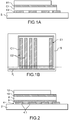
- the device comprises a substrate S, a layer of PVDF C1 between a metallic conductive layer forming common electrode E1 and a plurality of parallel electrically conductive strips forming individual electrodes E2.
- the device comprises a PVDF layer between a metallic conductive layer forming a common electrode and a plurality of conductive zones at the level of each pixel.
- the PVDF becomes pyroelectric after being polarized.
- the voltage to be applied to polarize the PVDF is between 75 V and 150 V per ⁇ m of thickness of PVDF. This polarization is carried out between the common electrode and the individual electrodes. In addition, if this polarization is to be carried out when piloting transistors are already in place, this voltage level can cause damage or even destruction of the transistors.
- all the individual electrodes E2 are short-circuited, for example by providing an electrical track P1 connecting all the individual electrodes as shown in the figure 1B , which makes it easier to apply a bias voltage across the PVDF layer.
- this short-circuiting must be removed in order to make the device usable, for this the electrical track is removed after the polarization.
- This electrical track P1 is removed by cutting the substrate (along the dotted line on the figure 1B ), this results in a loss of material and available space. In addition, this may result in chips and / or debris which can disturb the proper functioning of the device. In addition there is a risk that the cutting is not successful and that the device is unusable.
- the previously stated aim is achieved with a manufacturing process using a layer of a material capable of acquiring at least one electrical property after having been subjected to polarization, a common electrode and individual electrodes on either side of the material capable of acquiring electrical property, and a so-called polarization layer in contact with all the individual electrodes, the polarization layer having the property of being electrically conductive, and after application of a specific treatment, of being electrically insulating.
- PVDF polyvinylidene fluoride
- the manufacturing process uses a dedicated layer to polarize the material and give it its electrical property, this layer being rendered non-functional after the material has acquired its electrical property.
- such a material is a crosslinkable adhesive containing one or more initiation salts of photopolymerization, such as the epoxy adhesive LP 655 manufactured by DELO.
- the salts present in the formulation provide ionic conduction which disappears after UV exposure, which makes the electrical insulating glue during its crosslinking under UV.
- the polarization layer is arranged between the layer of material to be polarized and the individual electrodes. More advantageously, the layer is arranged between the substrate and the individual electrodes, which limits the interactions between the material to be polarized, for example PVDF and the material of the polarization layer, the effects of which are not known for long. term.
- the polarization layer can be located.
- the method according to the invention has the advantage of not requiring any cutting step or any other step liable to pollute the device.
- the elimination of short circuits is simple.
- the application of ultraviolet radiation in the case of LP 655 adhesive has no harmful effect on the rest of the components of the device.
- contact pads are provided intended to at least check after treatment if the polarization layer has actually become electrical insulator.
- the method according to the invention is advantageously implemented in the manufacture of thermal pattern sensors, in particular fingerprint sensors.
- the invention is all the more advantageous for devices implementing transistors, in fact the transistors are becoming smaller and more and more sensitive to the electric field.
- the short-circuiting thanks to the polarization layer makes it possible to protect them effectively.
- the material of the third layer becomes pyroelectric by applying a given polarization.
- the polarization layer is formed between the first layer and the third layer. According to another exemplary embodiment, the polarization layer is formed between the substrate and the first layer.
- the conductors of the first layer are made in the form of strips and the polarization layer is formed so as to be in contact with at least part of each of the strips.
- the polarization layer can be formed so as to be in contact with a longitudinal end of the strips.
- the method comprises the step of producing two electrical contacts in electrical contact with the bias layer, said electrical contacts being intended to at least verify the electrical conductivity of said bias layer at least after the treatment.
- the manufacturing method advantageously comprises the step of producing at least two transistors, each transistor being connected to an electrical conductor, the biasing layer being formed so as to be electrically connected at least to the drains of the transistors, and during the 'step c) the polarization layer, the drains, the sources and the grids are short-circuited.
- the polarization layer is a crosslinkable adhesive containing one or more crosslinking initiation salts, and the treatment is exposure to ultraviolet radiation.
- the material of the third layer may include poly (vinylidene fluoride) or one of its derivatives.
- the substrate is made of a material transparent to ultraviolet radiation and the exposure is carried out through the substrate.
- step d only portions of the polarization layer located between the conductors are made electrically insulating.
- the sun is made through a mask.
- the present invention also relates to a method of manufacturing a thermal pattern sensor comprising the manufacture of a device comprising a stack by the method according to the invention, the step of producing, on said stack, electrically conductive lines forming a heat source and the step of producing an encapsulation layer.
- the present invention also relates to a stack in order to produce a device comprising at least a first layer comprising at least two electrical conductors electrically isolated from each other, a second layer comprising at least one electrical conductor, a third layer of a material having at least one electrical property after electrical polarization, said third layer being disposed between the first layer and the second layer, said stack being obtained by implementing the manufacturing method according to the invention, said stack comprising the first layer, the second layer, the third layer, the material of the third layer not having said electrical property and a polarization layer of a material which has a first state in which it is electrically conductive and a second state in which it is electrically insulating, the transition from the first state to the second state being obtained by application of a treatment to said second material, said polarization layer being produced so as to be initially in its first state, said layer of polarization being in electrical contact with the electrical conductors of the first layer.
- the material of the third layer is poly (vinylidene fluoride) or one of its derivatives
- the material of the polarization layer is a crosslinkable adhesive containing one or more crosslinking initiation salts, for example an epoxy adhesive, said treatment being exposure to ultraviolet radiation.
- the invention will be described mainly in the context of the manufacture of a stack comprising PVDF in order to make it pyroelectric, with a view to an application to the production of fingerprint sensors, and more generally the production of thermal sensors.
- the invention can be applied to all devices the production of which requires a polarization step in order to acquire a material's electrical property, examples of which will be given below.
- an insulating or conductive material is an electrical insulating material or electrical conductor respectively, unless this is explicitly stated.
- the term “electrical property” of a material means a property by which the material is capable of generating a voltage or a current, for example when it is subjected to a temperature variation, it is a question pyroelectricity, or when subjected to deformation, it is piezoelectricity, or when it is the seat of permanent polarization after being subjected to polarization, such as the electrets.
- polarization such as the electrets.
- the stack EP1 comprises in this order a substrate 2, a layer 4 comprising a plurality of parallel electrically conductive strips 4.1 intended to form individual electrodes.
- the stack EP1 comprises a polarization layer 6, a layer 8 of material capable of having pyroelectric properties under the effect of a polarization, an electrically conductive layer 10 intended to form an electrode common to the right of the individual electrodes.
- a layer 12 intended to protect the stack is formed on the layer 10.
- the pyroelectric material of layer 8 can for example be a polyvinylidene fluoride or PVDF, a polyvinylidene-trifluoroethylene or P (VDF-TrFE), a ceramic such as PZT (lead titano-zirconate, or "Lead Zirconate Titanate "In English), crystals such as those known by the acronym TGS (Tris Glycine SDF) or LiTaO 3 crystals.
- PVDF polyvinylidene fluoride
- VDF-TrFE polyvinylidene-trifluoroethylene
- PZT lead titano-zirconate, or "Lead Zirconate Titanate "In English
- crystals such as those known by the acronym TGS (Tris Glycine SDF) or LiTaO 3 crystals.
- the common electrode 10 is connected to a given voltage, for example to ground.
- the substrate is for example electrical insulator, for example in a rigid material such as glass, or a flexible material, such as plastic material such as polyethylene (PET), poly (ethylene naphthalate) (PEN), polyurethane (PU) or polydimethyl (siloxane) (PDMS).
- plastic material such as polyethylene (PET), poly (ethylene naphthalate) (PEN), polyurethane (PU) or polydimethyl (siloxane) (PDMS).
- the device can be manufactured using a CMOS technology on a silicon substrate or on a silicon substrate on SOI insulator (Silicon on Insulator).
- each individual electrode means an electrode intended to form with the common electrode a part at most of the pixels.
- each individual electrode forms a column type pixel with the PVDF and the common electrode.
- heating lines perpendicular to the individual electrodes are formed, the crossing of a heating line and an individual electrode being considered as a pixel.
- the polarization layer 6 comprises a material which offers a state in which it is electrically conductive and a state, after application of a given treatment, in which it is electrically insulating.
- the term “electrical conductor” means a material which is sufficiently conductive to ensure a short-circuiting of the electrodes and / or of the transistors, and to allow the application of a bias voltage sufficient to make the material of the layer 8 pyroelectric in a few seconds up to 1 min. Even a material with very low electrical conductivity may be suitable.
- electrical insulating material means a material which is sufficiently insulating so that the quantity of charges produced at the level of a pixel can be detected separately from those generated at the level of the other pixels. For example, it is sought to have a current circulation in the polarization layer after treatment of at least 100 times less than the circulation in the individual electrodes.
- the material of the polarization layer 6 is a crosslinkable adhesive containing one or more crosslinking initiation salts, for example an epoxy adhesive.
- crosslinking initiation salts for example an epoxy adhesive.
- cationic photoinitiators such as the diaryliodonium or triarylsulfonium salts are initiation crosslinking salts suitable for the present invention.
- the initiation salt is ionic conductor, which makes the material weakly electrically conductive before crosslinking. After crosslinking, the material becomes electrically insulating.
- the epoxy adhesive produced by the company DELO is, for example, an adhesive whose salts added to the formulation are salts which initiate UV photopolymerization.
- the polarization layer comprises epoxy glue LP655 manufactured by DELO which passes from a conductive state to an electrical insulating state by crosslinking under exposure to ultraviolet (UV) radiation at a wavelength of about 365 nm.
- UV radiation ultraviolet
- the polarization layer 6 has for example a thickness of a hundred nm to a few ⁇ m.
- the figure 10 illustrates the evolution of electrical conductivity as a function of the level of crosslinking of the LP655 adhesive. It represents the variation of the current I in Amperes between two electric conductive bars connected by a drop of glue LP655 as a function of the voltage U in Volt.
- Each curve represents an electrical conductivity for a crosslinking time under UV.
- the To curve corresponds to the bars without drop of LP655, the current does not pass.
- T1 corresponding to a crosslinking time of 60 s, corresponds to the current flowing between the conductors with a drop of non-crosslinked LP 655 and therefore relatively conductive.
- the curves T2 to T5 correspond, in this order to states which are more and more crosslinked (crosslinking time under UV longer and longer) and less and less conductive. It can be seen that the electrical conductivity for the longest crosslinking time T5 is practically identical to the conductivity To, ie without drop. The material of layer 6 for a crosslinking time corresponding to T5 is therefore completely insulating.
- the polarization layer 6 extends so as to be in contact with all the individual electrodes, in order to short-circuit all the individual electrodes.
- the polarization layer 6 does not necessarily entirely cover the individual electrodes.
- the polarization layer 6 is formed between the substrate 2 and the individual electrodes.
- the polarization layer 6 provides the connection between all of the individual electrodes.
- the PVDF layer is formed on the individual electrodes. Due to the manufacturing process, it is also deposited between the individual electrodes and is in contact with the polarization layer 6.
- the PVDF layer is then made pyroelectric.
- a bias voltage is applied between the common electrode 10 and one of the individual electrodes, or even between the common electrode and the bias layer, to apply a sufficient voltage in order to make the PVDF pyroelectric.
- the bias voltage is around 300 V for a few seconds.
- the PVDF zones located to the right of the individual electrodes are made pyroelectric.
- This example is particularly advantageous, since the production of the polarization layer on the substrate is very simple and does not require structuring of the latter.
- the polarization layer 6 thus arranged does not form any additional capacitance between the individual electrodes and the common electrode.
- the entire polarization layer is made electrically insulating, for example by carrying out UV treatment through the substrate chosen to be transparent to UV.
- the polarization layer 6 is formed on the individual electrodes 4.1.
- the polarization layer is such that it allows all the individual electrodes to be connected.
- the polarization layer 6 only partially covers the individual electrode located at the right end in the representation of the figure 2 , but this partial overlap is sufficient to connect it to the other individual electrodes.
- the PVDF layer is then made pyroelectric.
- a bias voltage is applied between the common electrode 10 and one of the individual electrodes, or even between the common electrode and the bias layer, to apply a sufficient voltage in order to make the PVDF pyroelectric.
- the bias voltage is of the order of 300V.
- the implementation of the polarization layer simply makes it possible to apply a polarization voltage in a single step to all the zones of PVDF, in particular those located at the right of the individual electrodes.
- a treatment is applied to the polarization layer 6 in order to make it entirely electrically insulating.
- the polarization layer is made of LP 655 epoxy adhesive, it is crosslinked by UV exposure at a wavelength of about 365 nm.
- the duration of the insolation is chosen to ensure that the electrical conductivity of the adhesive is low enough to be considered as insulating, and that the individual electrodes are no longer electrically connected to each other.
- the duration of exposure is also sufficient for the adhesive to act as an adhesive and to be sufficiently hard.
- the polarization of PVDF is typically obtained by applying an electric field of 100 volts for a PVDF layer of 1 ⁇ m. In the case of a 3 nm PVDF layer, an electric field of around 300 volts is applied.
- the polarization layer is exposed through the substrate which is chosen to be transparent to UV radiation, for example this is made of glass or plastic, and through the individual electrodes which are chosen to be thin enough to be transparent to UV radiation.
- UV exposure is carried out through the common electrode when the material of the common electrode is sufficiently transparent to UV radiation, which is for example the case of an organic common electrode, for example made of PEDOT: PSS (mixture of poly (3,4-ethylenedioxythiophene) (PEDOT) and sodium poly (styrene sulfonate) (PSS)).
- PEDOT poly (3,4-ethylenedioxythiophene)
- PSS sodium poly (styrene sulfonate)
- the entire polarization layer 6 is made insulating.
- the presence of the polarizing layer 6 which is now electrically insulating adds a capacity in series, decreasing the total capacity of the pixel, which does not significantly disturb the operation of the device in the case of reading under load.
- its presence can be advantageous since the voltage produced is increased for the same amount of charge since the total capacity of the pixel is reduced. The detection sensitivity is then increased.
- this insulating layer in contact with the PVDF makes it possible to further reduce the leakage current through the PVDF, which is already low due to the very good electrical insulation provided by the PVDF.
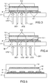
- a substrate 2 sufficiently transparent to UV radiation, such as glass or a plastic material, to allow sunshine through the substrate, as shown by the UV arrows, and we choose individual metal electrodes that are sufficiently thick. so as not to be transparent to UV.
- the UV1 rays insolate the polarization layer 6, and the UV2 rays are stopped by the electrodes 4.1. It follows that at the end of the insolation step, the polarization layer 6 retains conductive areas 6.1 in line with the individual electrodes, separated by insulating areas 6.2 between the individual electrodes.
- the conductive areas 6.1 form an extension of the individual electrodes, in the direction of the thickness of the electrodes.
- a mask M is used to mask the polarization layer from UV radiation.
- the mask M is placed under the substrate and is in line with each individual electrode.
- the mask is placed above the common electrode when the exposure is made through the common electrode.
- the mask is for example used when the individual electrodes are too transparent to UV rays to prevent crosslinking.
- the mask is similar to those commonly used in microelectronic processes.
- the UV1 rays insolate the polarization layer 6, and the UV2 rays are stopped by the mask.
- the polarization layer 6 comprises electrical insulating portions 6.2 which electrically insulate the individual electrodes 4.1.
- the processing depends on the material of the polarization layer. In the case of sunshine, it will be made at a wavelength capable of crosslinking the material, which may be different from that of UV radiation.
- two electrical contact pads 14 are formed in the polarization layer 6 outside of the stack with the PVDF layer, and on either side of the stack in the plane of the polarization layer. For example, by applying a voltage between the pads 14, a current greater than a given threshold is measured if the bias layer is electrically conductive, and a current is measured below the given threshold if the bias layer is insulating.
- the contact pads 14 also make it possible to measure the conduction of the polarization layer before the polarization of the PVDF and to verify that it is sufficiently conductive, one of the contact pads can be used with the common electrode, to apply the bias voltage to the PVDF layer.
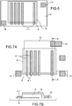
- the polarization layer 6 ′ is located, ie it is not a full plate layer. In the example shown, it is formed at the longitudinal ends 4.3 of the individual electrodes.
- the polarization layer is for example produced by using a mask to deposit glue in a localized manner, unlike the previous embodiments in which the glue is deposited full plate.
- the polarization layer is in the form of a strip.
- the polarization layer may have any other shape allowing it to be in contact with all the individual electrodes 4.1.
- the localized polarization layer is deposited between the substrate and the individual electrodes as in the example of the figure 5 .
- the rest of the stack accommodates this localized excess thickness.
- This exemplary embodiment reduces the amount of material used to produce the polarization layer.
- the common electrode 10 is extended by a resumption of contact 16 which rests on the substrate 2, and which allows the connection of the common electrode 10 to ground or to a fixed potential. Connection, for example by soldering, is facilitated, since the resumption of contact 16 rests on a rigid element, ie the substrate made of glass or other rigid material, unlike PVDF.
- the surface of the PVDF layer is chosen so that the contact resumption 16 of the common electrode 10 is at a sufficient distance from the individual electrode 4.1, in order to reduce the risks of short circuit between the common electrode 10 and the individual electrode 4.1.
- the use of a large surface PVDF layer also makes it possible to isolate the contact resumption of any heating lines formed on the stack.
- the bias layer is deposited between the individual electrodes and the PVDF layer.
- contact pads 14 are produced at the two ends of the polarization layer as in the example of the figure 6 , and make it possible to check the electrical conductivity of the polarization layer before and / or after the treatment.
- the contact resumption 16 and the common electrode 10 are connected by a portion of the same material as the polarization layer 6, in order to make a temporary connection.
- the polarization layer can be exposed directly from above, or from below through the substrate.
- the zones of the polarization layer between the individual electrodes are made electrically insulating and interrupt the short circuit between the electrodes.
- the electrodes mask the UV polarization layer, the zones of the polarization layer located only in line with the individual electrodes are not rendered insulating, but the operation of the device is not disturbed.
- a substrate transparent to UV rays is chosen and the rear face is exposed through the substrate which allows the entire polarization strip to be exposed.
- the electronic part includes transistors T, for example one transistor per pixel, each individual electrode then being connected to a transistor.
- the electronic part includes a support substrate 102, for example made of glass, a layer 103, for example of polyimide for example from 15 ⁇ m to 20 ⁇ m thick, T transistors, for example in thin layers or TFT (thin films transistor in Anglo-Saxon terminology) produced for example in IGZO (Indium-Gallium-Zinc oxide), a layer of SiN 105, and vias V1 and V2 through the layer of SiN, resuming contact with the drain D and the source So.
- the grid G has a connection opening onto the edge of the device.
- Each drain D is connected to a lower electrode 104.1 by a via V3.
- the device also includes an insulating interface layer 107 between the electronic part II and the detection part I, for example a polymer layer.
- the PVDF layer 108 is placed between the common electrode 110 and the individual electrodes 104.1.
- the device also includes a polarization layer 106 on the interface layer and under and in contact with the individual electrodes. All the individual electrodes 104 are connected to each other by the polarization layer 106. In addition, the drains D are connected to the polarization source 106 by the via V3.
- the transistors are distributed in rows and columns. All the transistors of a column are connected by their source So and all the transistors of a line are connected by their grid, called selection line.
- the source columns and the grid lines lead to the sides of the stack.
- using the polarization layer 106 or one or more other polarization layers it is possible to connect all the sources on the one hand and all the gates on the other hand.
- the PVDF is polarized, the drains, sources and grids are grounded.
- This example of polarization is particularly interesting because the polarization layer makes it possible to reach the individual electrodes which are normally buried in the stack. Thus it is possible to apply a bias to the PVDF by applying a voltage to the individual electrodes via the bias layer which is accessible on one side of the stack.
- the polarization layer 106 is interposed between the electronic part II and the detection part I.
- the polarization layer 106 is in contact with the vias V1, V2 and V3.
- the individual electrodes 104.1, the sources So and the drains D are then short-circuited via layer 106.
- the grid lines lead to the sides of the stack.
- Using the polarization layer 106 or one or more other polarization layers it is possible to connect all the gates together and to earth them. When the PVDF is polarized, the drains, sources and grids are grounded.
- a via is provided at the level of the grid which opens into the polarization layer, which makes it possible to put the grid, the drain and the source simultaneously in short-circuit. Since all the grids of each selection line are connected, a single via is enough between a grid of a line and the polarization layer. The via is for example carried out at the end of a line.
- the fingerprint sensor of the figure 9 it comprises a substrates 202, a polarization layer 206 directly on the substrate 202 which can be entirely cover the substrate, as shown in the figure 9 , or be located, individual electrodes 204.1, for example made of gold 50 nm thick, a layer 208 of P (VDF-TrFE), for example between 2 ⁇ m and 3 ⁇ m, a layer of solid plate conductor 210 forming the electrode common, for example 0.3 ⁇ m of PEDOT: PSS, a dielectric layer 214 for example of polyimide with a thickness of the order of 0.2 ⁇ m, conductive lines 216 oriented at right angles to the individual electrodes 204.1, and forming the heating means.
- the conductive lines are, for example, in silver 1 ⁇ m thick or in gold 50 nm thick, and an encapsulation layer 212.
- the individual electrodes and the conductive lines are finely structured at the pixel pitch. For example, we make a matrix of 128 ⁇ 128 pixels with a pitch of 90 ⁇ m. individual electrodes are then produced having a width of 60 ⁇ m spaced 30 microns apart. The metal tracks perpendicular to the electrodes are 128 in number and have a width of 45 ⁇ m and are spaced 45 ⁇ m apart.
- the PVDF layer has a thickness of 3 ⁇ m.
- the relative permittivity ⁇ r of P (VDF-TrFE) is between 10 and 12.
- the vacuum permittivity ⁇ 0 is 8.85418782 ⁇ 10 -12 m -3 kg -1 s 4 A 2 .
- VDF-TrFE VDF-TrFE
- the device is connected to a Texas Instruments DDC264® analog converter (64 channels, 20 bit ADC), on an EVM card of the same name with 256 inputs.
- a Texas Instruments DDC264® analog converter 64 channels, 20 bit ADC
- the pyroelectric coefficient of P (VDF-TrFE) is around 29.10 6 C / m 2 / K
- the reading times are of the order of a millisecond, i.e. the time for the thermal signal to propagate towards the P (VDF - TrFE).
- the polymerized adhesive is therefore sufficiently insulating to ensure the operation of the device.
- the individual electrodes can have any shape.
- the polarization layer on the individual electrodes relative to the substrate can be produced only on the longitudinal ends of the column electrodes.
- Having the common electrode on the pyroelectric material has the advantage of shielding the device against electrical noise coming from the finger, in an application to a fingerprint sensor.
- the common electrode is on the pyroelectric material with respect to the substrate. According to other examples, it is located under the pyroelectric material on the side of the substrate, and the individual electrodes are on the pyroelectric material.
- the common electrode comprises as many electrodes as individual electrodes, said electrodes being connected to a fixed voltage.
- the manufacturing process can be implemented to manufacture thermal pattern sensors, for example fingerprint sensors, cameras using PVDF.
- the present invention applies to other materials which are capable of acquiring an electrical property after being subjected to polarization.
- the invention applies to materials capable of becoming piezoelectric under the application of a voltage: PVDF and PZT also become piezoelectric when they are subjected to a bias voltage.
- An electret is a dielectric material which remains permanently electrified after being subjected to a temporary electric field.
- Such material are for example formed by polymers, for example from the VHB® family, advantageously VHB4910®.
- Piezoelectric devices thus produced can be used as a “pressure” or ultrasonic fingerprint sensor, the piezoelectric material is then used as an ultrasonic emitter, the same piezoelectric material can be used as a receiver or not.
- Piezoelectric devices thus produced can also be used as actuators.
Abstract
Procédé de fabrication d'un dispositif comportant un empilement comprenant une première couche (4) comportant des conducteurs électriques (4.1) isolés électriquement l'un de l'autre, une deuxième couche (10) conductrice électrique, une troisième couche (8) de matériau pyroélectrique, ladite troisième couche (8) étant disposée entre la première couche (4) et la deuxième couche (10), ledit procédé comportant :a) la réalisation, sur un substrat, dudit empilement, le matériau de la troisième couche n'étant pas à ce stade pyroélectrique,b) la réalisation d'une couche de polarisation (6) en colle époxy en contact électrique avec les conducteurs électriques (4.1) de la première couche (4),c) une étape d'application d'une tension de polarisation à ladite troisième couche (8) de sorte que son matériau devienne pyroélectrique,d) une étape d'insolation par un rayonnement ultraviolet de la couche de polarisation (6) dans son deuxième état de sorte à la rendre au moins en partie isolante électrique.Method for manufacturing a device comprising a stack comprising a first layer (4) comprising electrical conductors (4.1) electrically insulated from each other, a second electrically conductive layer (10), a third layer (8) of pyroelectric material, said third layer (8) being disposed between the first layer (4) and the second layer (10), said method comprising: a) producing, on a substrate, said stack, the material of the third layer n ' not being at this pyroelectric stage, b) producing a polarization layer (6) of epoxy adhesive in electrical contact with the electrical conductors (4.1) of the first layer (4), c) a step of applying a bias voltage at said third layer (8) so that its material becomes pyroelectric, d) a step of insulating by ultraviolet radiation the bias layer (6) in its second state so as to return it at least in electrical insulating part .
Description
La présente invention se rapporte à un procédé de fabrication d'un dispositif comprenant au moins une couche de matériau acquérant une propriété électrique après avoir été soumis à une polarisation, par exemple comprenant un matériau devenant pyroélectrique par polarisation.The present invention relates to a method of manufacturing a device comprising at least one layer of material acquiring an electrical property after being subjected to polarization, for example comprising a material becoming pyroelectric by polarization.
Par exemple dans le domaine des capteurs d'empreintes, et plus généralement des capteurs de motifs thermiques on utilise l'effet pyroélectrique, i.e. la génération de charges du fait d'une variation de température.For example, in the field of fingerprint sensors, and more generally thermal pattern sensors, the pyroelectric effect is used, i.e. the generation of charges due to a temperature variation.
Un capteur d'empreintes thermique comporte une matrice de pixels, chacun apte à générer des charges par variation de température. Chaque pixel comporte un matériau pyroélectrique entre deux électrodes, chaque pixel est adressable individuellement pour permette de détecter la quantité de charge produite par chacun des pixels. Une empreinte digitale comporte des crêtes et des vallées et le contact entre un pixel et une crête ou une vallée provoque une variation de température, qui est différente selon qu'il s'agit d'une crête ou d'une vallée. De préférence, les pixels sont chauffés afin d'éviter un équilibre thermique entre le capteur et la surface du doigtA thermal fingerprint sensor comprises a matrix of pixels, each capable of generating charges by variation of temperature. Each pixel has a pyroelectric material between two electrodes, each pixel is individually addressable to detect the amount of charge produced by each of the pixels. A fingerprint has peaks and valleys and the contact between a pixel and a peak or valley causes a temperature variation, which is different depending on whether it is a peak or a valley. Preferably, the pixels are heated in order to avoid a thermal equilibrium between the sensor and the surface of the finger
Le PVDF (poly(fluorure de vinylidène)) et ses divers copolymères comme le PVDF-TrFE (tri fluoro éthylène) présentent des propriétés pyroélectriques, ces propriétés apparaissent après application d'une certaine tension de polarisation.PVDF (poly (vinylidene fluoride)) and its various copolymers such as PVDF-TrFE (tri fluoro ethylene) have pyroelectric properties, these properties appear after application of a certain bias voltage.
Par ailleurs, afin de piloter chacun des pixels ou groupe de pixels un ou plusieurs transistors peuvent être mis en œuvre.Furthermore, in order to drive each of the pixels or group of pixels, one or more transistors can be implemented.
Par exemple, au moins trois transistors peuvent être mis en œuvre au niveau de chaque pixel pour lire la tension : un transistor assurant l'amplification du signal, un deuxième transistor permettant la sélection du pixel et un troisième transistor permettant de mettre la tension à une valeur connue en début d'acquisition.For example, at least three transistors can be implemented at the level of each pixel to read the voltage: a transistor ensuring the amplification of the signal, a second transistor allowing the selection of the pixel and a third transistor allowing to put the voltage at a known value at the start of acquisition.
Sur la
Comme indiqué ci-dessus, le PVDF devient pyroélectrique après avoir été polarisé. La tension à appliquer pour polariser le PVDF est comprise entre 75 V et 150 V par µm d'épaisseur de PVDF. Cette polarisation est réalisée entre l'électrode commune et les électrodes individuelles. En outre, si cette polarisation est à réaliser alors que des transistors de pilotage sont déjà en place, ce niveau de tension peut provoquer un endommagement, voire une destruction des transistors.As indicated above, the PVDF becomes pyroelectric after being polarized. The voltage to be applied to polarize the PVDF is between 75 V and 150 V per µm of thickness of PVDF. This polarization is carried out between the common electrode and the individual electrodes. In addition, if this polarization is to be carried out when piloting transistors are already in place, this voltage level can cause damage or even destruction of the transistors.
Afin d'éviter d'avoir à connecter individuellement chaque pixel ou groupe de pixels à une source de polarisation, préalablement à l'étape de polarisation, toutes les électrodes individuelles E2 sont mises en court-circuit, par exemple en prévoyant une piste électrique P1 reliant toutes les électrodes individuelles comme cela est représenté sur la
Dans le cas d'un dispositif présentant par exemple un transistor de sélection par pixel dans lequel la source est connectée à l'électrode individuelle E2 du pixel, le drain est relié à une colonne et la grille est connectée à une ligne électrique de sélection, afin d'éviter la destruction du transistor, il faut rendre tous les transistors du plan pixel conducteurs en appliquant une tension de grille adaptée, et donc en reliant momentanément toutes les grilles, ainsi que toutes les colonnes, ce qui rend le procédé complexe.In the case of a device having for example a pixel selection transistor in which the source is connected to the individual electrode E2 of the pixel, the drain is connected to a column and the grid is connected to an electrical line of selection, in order to avoid the destruction of the transistor, all the transistors of the pixel plane must be made conductive by applying a suitable gate voltage, and therefore by temporarily connecting all the gates, as well as all the columns, which makes the process complex .
C'est par conséquent un but de la présente invention d'offrir un procédé de fabrication d'un dispositif comportant un matériau apte à acquérir au moins une propriété électrique, ne présentant pas les inconvénients énumérés ci-dessus.It is therefore an object of the present invention to provide a method of manufacturing a device comprising a material capable of acquiring at least one electrical property, not having the drawbacks listed above.
Le but précédemment énoncé est atteint avec un procédé de fabrication mettant en œuvre une couche d'un matériau apte à acquérir au moins une propriété électrique après avoir été soumis à une polarisation, une électrode commune et des électrodes individuelles de part et d'autre du matériau apte acquérir la propriété électrique, et une couche dite de polarisation en contact avec toutes les électrodes individuelles, la couche de polarisation présentant la propriété d'être conductrice électrique, et après application d'un traitement spécifique, d'être isolante électrique.The previously stated aim is achieved with a manufacturing process using a layer of a material capable of acquiring at least one electrical property after having been subjected to polarization, a common electrode and individual electrodes on either side of the material capable of acquiring electrical property, and a so-called polarization layer in contact with all the individual electrodes, the polarization layer having the property of being electrically conductive, and after application of a specific treatment, of being electrically insulating.
Par exemple, en utilisant une telle couche de polarisation dans un empilement comprenant une couche de poly(fluorure de vinylidène) (PVDF), il est possible de mettre simplement en court-circuit toutes les électrodes individuelles et éventuellement les transistors le cas échéant, et ainsi de pouvoir appliquer une tension suffisante pour polariser le PVDF, qui devient alors pyroélectrique. En appliquant un traitement spécifique à cette couche de polarisation, elle devient isolante électrique, ce qui supprime la mise en court-circuit des électrodes et éventuellement des transistors, rendant le dispositif fonctionnel.For example, by using such a polarization layer in a stack comprising a layer of polyvinylidene fluoride (PVDF), it is possible to simply short-circuit all the individual electrodes and possibly the transistors if necessary, and thus being able to apply sufficient voltage to polarize the PVDF, which then becomes pyroelectric. By applying a specific treatment to this polarization layer, it becomes electrically insulating, which eliminates the short-circuiting of the electrodes and possibly of the transistors, making the device functional.
En d'autres termes, le procédé de fabrication met en œuvre une couche dédiée pour polariser le matériau et lui donner sa propriété électrique, cette couche étant rendue non fonctionnelle après que le matériau ait acquis sa propriété électrique.In other words, the manufacturing process uses a dedicated layer to polarize the material and give it its electrical property, this layer being rendered non-functional after the material has acquired its electrical property.
Par exemple, un tel matériau est une colle réticulable contenant un ou des sels d'initiation de la photopolymérisation, telle que la colle époxy LP 655 fabriquée par DELO. Les sels présents dans la formulation assurent une conduction ionique qui disparait après insolation UV, ce qui rend la colle isolante électrique lors de sa réticulation sous UV.For example, such a material is a crosslinkable adhesive containing one or more initiation salts of photopolymerization, such as the epoxy adhesive LP 655 manufactured by DELO. The salts present in the formulation provide ionic conduction which disappears after UV exposure, which makes the electrical insulating glue during its crosslinking under UV.
Dans un exemple, la couche de polarisation est disposée entre la couche de matériau à polariser et les électrodes individuelles. De manière plus avantageuse, la couche est disposée entre le substrat et les électrodes individuelles, ce qui limite les interactions entre le matériau à polariser, par exemple le PVDF et le matériau de la couche de polarisation, dont on ne connaît pas les effets à long terme.In one example, the polarization layer is arranged between the layer of material to be polarized and the individual electrodes. More advantageously, the layer is arranged between the substrate and the individual electrodes, which limits the interactions between the material to be polarized, for example PVDF and the material of the polarization layer, the effects of which are not known for long. term.
Afin de réaliser ce court-circuit, il suffit de réaliser une couche de polarisation pleine plaque. Avantageusement, la couche de polarisation peut être localisée.In order to achieve this short circuit, it suffices to produce a full plate polarization layer. Advantageously, the polarization layer can be located.
Le procédé selon l'invention présente l'avantage de ne nécessiter aucune étape de découpe ou toute autre étape susceptible de polluer le dispositif. La suppression des courts-circuits se fait de manière simple. L'application d'un rayonnement ultra-violet dans le cas de la colle LP 655 n'a pas d'effet dommageable sur le reste des composants du dispositif.The method according to the invention has the advantage of not requiring any cutting step or any other step liable to pollute the device. The elimination of short circuits is simple. The application of ultraviolet radiation in the case of LP 655 adhesive has no harmful effect on the rest of the components of the device.
Selon une caractéristique additionnelle, on prévoit des plots de contact destinés à au moins vérifier après traitement si la couche de polarisation est effectivement devenue isolante électrique.According to an additional characteristic, contact pads are provided intended to at least check after treatment if the polarization layer has actually become electrical insulator.
Le procédé selon l'invention est avantageusement mis en œuvre dans la fabrication de capteurs de motifs thermique, en particuliers les capteurs d'empreintes digitales.The method according to the invention is advantageously implemented in the manufacture of thermal pattern sensors, in particular fingerprint sensors.
L'invention est d'autant plus intéressante pour des dispositifs mettant en œuvre des transistors, en effet les transistors sont de plus en plus petits et de plus en plus sensibles au champ électrique. La mise en court-circuit grâce à la couche de polarisation permet de les protéger efficacement.The invention is all the more advantageous for devices implementing transistors, in fact the transistors are becoming smaller and more and more sensitive to the electric field. The short-circuiting thanks to the polarization layer makes it possible to protect them effectively.
La présente invention a alors pour objet un procédé de fabrication d'un dispositif comportant un empilement comprenant une première couche comportant au moins deux conducteurs électriques isolés électriquement l'un de l'autre, une deuxième couche comportant au moins un conducteur électrique, au moins une troisième couche de matériau présentant au moins une propriété électrique, ladite troisième couche étant disposée entre la première couche et la deuxième couche, ledit procédé comportant :
- a) une étape de réalisation, sur un substrat, d'un empilement comprenant la première couche, la deuxième couche et la troisième couche d'un matériau qui, après polarisation électrique, devient ledit matériau présentant ladite propriété électrique, la première couche et la deuxième couche étant disposées l'une par rapport à l'autre de sorte à permettre l'application d'une tension de polarisation au sein de la troisième couche,
- b) une étape de réalisation d'une couche de polarisation en contact électrique avec les au moins deux conducteurs électriques de la première couche, ladite couche de polarisation comportant un matériau qui présente un premier état dans lequel il est conducteur électrique et un deuxième état dans lequel il est isolant électrique, le passage du premier état au deuxième état étant obtenu par application d'un traitement à ladite couche de polarisation, ladite couche de polarisation étant réalisée de sorte à être initialement dans son premier état,
- c) une étape d'application d'une tension de polarisation à ladite troisième couche de sorte que son matériau présente ladite propriété électrique,
- d) une étape d'application dudit traitement transformant au moins une partie du matériau de la couche de polarisation dans son deuxième état, de sorte que lesdits au moins deux conducteurs électriques de la première couche sont isolés électriquement les uns des autres.
- a) a step of producing, on a substrate, a stack comprising the first layer, the second layer and the third layer of a material which, after electrical polarization, becomes said material having said electrical property, the first layer and the second layer being arranged relative to each other so as to allow the application of a bias voltage within the third layer,
- b) a step of producing a polarization layer in electrical contact with the at least two electric conductors of the first layer, said polarization layer comprising a material which has a first state in which it is electrically conductive and a second state in which it is electrically insulating, the transition from the first state to the second state being obtained by applying a treatment to said polarization layer, said polarization layer being produced so as to be initially in its first state,
- c) a step of applying a bias voltage to said third layer so that its material has said electrical property,
- d) a step of applying said treatment transforming at least part of the material of the polarization layer in its second state, so that said at least two electrical conductors of the first layer are electrically isolated from each other.
Par exemple, le matériau de la troisième couche devient pyroélectrique en appliquant une polarisation donnée.For example, the material of the third layer becomes pyroelectric by applying a given polarization.
Selon un exemple de réalisation, la couche de polarisation est formée entre la première couche et la troisième couche. Selon un autre exemple de réalisation, la couche de polarisation est formée entre le substrat et la première couche.According to an exemplary embodiment, the polarization layer is formed between the first layer and the third layer. According to another exemplary embodiment, the polarization layer is formed between the substrate and the first layer.
Selon une caractéristique additionnelle, les conducteurs de la première couche sont réalisés en forme de bandes et la couche de polarisation est formée de sorte à être en contact avec une partie au moins de chacune des bandes. Dans un exemple avantageux, la couche de polarisation peut être formée de sorte à être en contact avec une extrémité longitudinale des bandes.According to an additional characteristic, the conductors of the first layer are made in the form of strips and the polarization layer is formed so as to be in contact with at least part of each of the strips. In an example advantageously, the polarization layer can be formed so as to be in contact with a longitudinal end of the strips.
Selon une caractéristique additionnelle, le procédé comporte l'étape de réalisation de deux contacts électriques en contact électrique avec la couche de polarisation, lesdits contacts électriques étant destinés à au moins vérifier la conductivité électrique de ladite couche de polarisation au moins après le traitement.According to an additional characteristic, the method comprises the step of producing two electrical contacts in electrical contact with the bias layer, said electrical contacts being intended to at least verify the electrical conductivity of said bias layer at least after the treatment.
Le procédé de fabrication comporte avantageusement l'étape de réalisation d'au moins deux transistors, chaque transistor étant connecté à un conducteur électrique, la couche de polarisation étant formée de sorte à être connectée électriquement au moins aux drains des transistors, et lors de l'étape c) la couche de polarisation, les drains, les sources et les grilles sont en court-circuit.The manufacturing method advantageously comprises the step of producing at least two transistors, each transistor being connected to an electrical conductor, the biasing layer being formed so as to be electrically connected at least to the drains of the transistors, and during the 'step c) the polarization layer, the drains, the sources and the grids are short-circuited.
Dans un exemple particulièrement avantageux, la couche de polarisation est une colle réticulable contenant un ou plusieurs sels d'initiation de réticulation, et le traitement est une insolation au rayonnement ultraviolet. Le matériau de la troisième couche peut comporter du poly(fluorure de vinylidène) ou l'un de ses dérivés.In a particularly advantageous example, the polarization layer is a crosslinkable adhesive containing one or more crosslinking initiation salts, and the treatment is exposure to ultraviolet radiation. The material of the third layer may include poly (vinylidene fluoride) or one of its derivatives.
Dans un exemple de réalisation, le substrat est en un matériau transparent au rayonnement ultraviolet et l'insolation est réalisée à travers le substrat.In an exemplary embodiment, the substrate is made of a material transparent to ultraviolet radiation and the exposure is carried out through the substrate.
Il peut être envisagées que, lors de l'étape d), seules des portions de la couche de polarisation situées entre les conducteurs sont rendues isolantes électriques.It can be envisaged that, during step d), only portions of the polarization layer located between the conductors are made electrically insulating.
Selon une caractéristique additionnelle, l'insolation se fait à travers un masque.According to an additional characteristic, the sun is made through a mask.
La présente invention a également pour objet un procédé de fabrication d'un capteur de motifs thermiques comportant la fabrication d'un dispositif comprenant un empilement par le procédé selon l'invention, l'étape de réalisation, sur ledit empilement, des lignes conductrices électriques formant une source de chaleur et l'étape de réalisation d'une couche d'encapsulation.The present invention also relates to a method of manufacturing a thermal pattern sensor comprising the manufacture of a device comprising a stack by the method according to the invention, the step of producing, on said stack, electrically conductive lines forming a heat source and the step of producing an encapsulation layer.
La présente invention a également pour objet un empilement en vue de réaliser un dispositif comportant au moins une première couche comportant au moins deux conducteurs électriques isolés électriquement l'un de l'autre, une deuxième couche comportant au moins un conducteur électrique, une troisième couche en un matériau présentant après polarisation électrique au moins une propriété électrique, ladite troisième couche étant disposée entre la première couche et la deuxième couche, ledit empilement étant obtenu en mettant en œuvre le procédé de fabrication selon l'invention, ledit empilement comportant la première couche, la deuxième couche, la troisième couche, le matériau de la troisième couche ne présentant pas ladite propriété électrique et une couche de polarisation en un matériau qui présente un premier état dans lequel il est conducteur électrique et un deuxième état dans lequel il est isolant électrique, le passage du premier état au deuxième état étant obtenu par application d'un traitement audit deuxième matériau, ladite couche de polarisation étant réalisée de sorte à être initialement dans son premier état, ladite couche de polarisation étant en contact électrique avec les conducteurs électriques de la première couche.The present invention also relates to a stack in order to produce a device comprising at least a first layer comprising at least two electrical conductors electrically isolated from each other, a second layer comprising at least one electrical conductor, a third layer of a material having at least one electrical property after electrical polarization, said third layer being disposed between the first layer and the second layer, said stack being obtained by implementing the manufacturing method according to the invention, said stack comprising the first layer, the second layer, the third layer, the material of the third layer not having said electrical property and a polarization layer of a material which has a first state in which it is electrically conductive and a second state in which it is electrically insulating, the transition from the first state to the second state being obtained by application of a treatment to said second material, said polarization layer being produced so as to be initially in its first state, said layer of polarization being in electrical contact with the electrical conductors of the first layer.
Par exemple, le matériau de la troisième couche est du poly(fluorure de vinylidène) ou l'un de ses dérivés, et le matériau de la couche de polarisation est une colle réticulable contenant un ou plusieurs sels d'initiation de réticulation, par exemple une colle époxy, ledit traitement étant une insolation au rayonnement ultra-violet.For example, the material of the third layer is poly (vinylidene fluoride) or one of its derivatives, and the material of the polarization layer is a crosslinkable adhesive containing one or more crosslinking initiation salts, for example an epoxy adhesive, said treatment being exposure to ultraviolet radiation.
La présente invention sera mieux comprise sur la base de la description qui va suivre et des dessins en annexe sur lesquels :
- La
figure 1A est une représentation schématique en vue de côté, d'un empilement de l'état de la technique, comportant une couche de PVDF à polariser, - La
figure 1B est une représentation schématique en vue de dessus, de l'empilement de lafigure 1A , - La
figure 2 est une représentation schématique en vue de côté, d'un empilement selon l'invention comportant une couche de PVDF à polariser, - La
figure 3 est une représentation schématique de l'empilement de lafigure 2 lors d'un exemple d'étape de traitement visant à rendre isolante la couche de polarisation, - La
figure 4 est une représentation schématique de l'empilement de lafigure 2 lors d'un autre exemple d'étape de traitement visant à rendre isolante la couche de polarisation, - La
figure 5 est une représentation schématique en vue de côté, d'un autre exemple d'empilement selon l'invention comportant une couche de PVDF à polariser, - La
figure 6 est une représentation schématique d'une variante de réalisation de lafigure 5 mettant en œuvre des plots de contact, - La
figure 7A est une représentation schématique vue de dessus d'un autre exemple de réalisation d'un empilement selon l'invention, - La
figure 7B est une vue en coupe le long du plan A-A de lafigure 7A , - Les
figures 8A et 8B sont des représentations schématiques de deux autres exemples de réalisation d'empilements selon l'invention mettant en œuvre des transistors, - La
figure 9 est une représentation schématique d'un autre exemple de réalisation d'un empilement selon l'invention mettant en œuvre des transistors, - La
figure 10 est une représentation graphique de la variation du courant I en fonction de la tension U dans une couche de polarisation après différentes durées d'insolation.
- The
figure 1A is a schematic representation in side view of a stack of the state of the art, comprising a layer of PVDF to be polarized, - The
figure 1B is a schematic representation in top view of the stacking of thefigure 1A , - The
figure 2 is a schematic representation in side view of a stack according to the invention comprising a layer of PVDF to be polarized, - The
figure 3 is a schematic representation of the stacking of thefigure 2 during an example of a processing step aimed at rendering the polarization layer insulating, - The
figure 4 is a schematic representation of the stacking of thefigure 2 during another example of a processing step aimed at rendering the polarization layer insulating, - The
figure 5 is a schematic representation in side view of another example of stacking according to the invention comprising a layer of PVDF to be polarized, - The
figure 6 is a schematic representation of an alternative embodiment of thefigure 5 using contact pads, - The
figure 7A is a schematic representation seen from above of another embodiment of a stack according to the invention, - The
figure 7B is a sectional view along the AA plane of thefigure 7A , - The
Figures 8A and 8B are schematic representations of two other exemplary embodiments of stacks according to the invention using transistors, - The
figure 9 is a schematic representation of another exemplary embodiment of a stack according to the invention using transistors, - The
figure 10 is a graphic representation of the variation of the current I as a function of the voltage U in a polarization layer after different durations of sunshine.
Dans la description qui va suivre, l'invention sera décrite principalement dans le cadre de la fabrication d'un empilement comportant du PVDF afin de le rendre pyroélectrique, en vue d'une application à la réalisation de capteurs d'empreintes, et plus généralement à la réalisation de capteurs thermiques. Mais l'invention peut s'appliquer à tous les dispositifs dont la fabrication requiert une étape de polarisation pour faire acquérir à un matériau une propriété électrique, dont des exemples seront donnés ci-dessous.In the following description, the invention will be described mainly in the context of the manufacture of a stack comprising PVDF in order to make it pyroelectric, with a view to an application to the production of fingerprint sensors, and more generally the production of thermal sensors. However, the invention can be applied to all devices the production of which requires a polarization step in order to acquire a material's electrical property, examples of which will be given below.
Dans la description qui va suivre, un matériau isolant ou conducteur est un matériau isolant électrique ou conducteur électrique respectivement, à moins que cela soit précisé explicitement.In the following description, an insulating or conductive material is an electrical insulating material or electrical conductor respectively, unless this is explicitly stated.
Le procédé de fabrication selon l'invention comporte les étapes générales suivantes :
- réalisation d'un empilement comportant un matériau apte à acquérir au moins une propriété électrique et disposé entre une électrode commune et au moins deux électrodes individuelles,
- réalisation d'une couche de polarisation mettant en court-circuit les électrodes individuelles et éventuellement les transistors. La couche de polarisation est par exemple réalisée par un procédé d'impression ou d'enduction choisi en fonction de la viscosité du matériau de la couche. La couche de polarisation est réalisée par exemple par enduction au rouleau, enduction à fente (slot-die en anglais) ou par sérigraphie,
- application d'une polarisation à la couche apte à acquérir la propriété électrique en utilisant la couche de polarisation,
- application d'un traitement pour rendre la couche de polarisation isolante électrique.
- production of a stack comprising a material capable of acquiring at least one electrical property and disposed between a common electrode and at least two individual electrodes,
- realization of a polarization layer shorting the individual electrodes and possibly the transistors. The polarization layer is for example produced by a printing or coating process chosen as a function of the viscosity of the material of the layer. The polarization layer is produced for example by roller coating, slot coating in slot-die or by screen printing,
- application of a polarization to the layer capable of acquiring the electrical property by using the polarization layer,
- application of a treatment to make the polarizing insulating layer electric.
Dans la présente demande, on entend par « propriété électrique » d'un matériau, une propriété par laquelle le matériau est capable de générer une tension ou un courant, par exemple lorsqu'il est soumis à un variation de température, il s'agit de la pyroélectricité, ou lorsqu'il est soumis à une déformation, il s'agit de la piézoélectricité, ou lorsqu'il est le siège de polarisation permanente après avoir été soumis à une polarisation, tels que les électrets. Sur la
L'empilement EP1 comporte dans cet ordre un substrat 2, une couche 4 comportant une pluralité de bandes 4.1 conductrices électriques parallèles destinées à former des électrodes individuelles. L'empilement EP1 comporte une couche de polarisation 6, une couche 8 de matériau apte à avoir des propriétés pyroélectriques sous l'effet d'une polarisation, une couche conductrice électrique 10 destinée à former une électrode commune au droit des électrodes individuelles. Dans l'exemple représenté, une couche 12 destinée à protéger l'empilement est formée sur la couche 10.The stack EP1 comprises in this order a
Le matériau pyroélectrique de la couche 8 peut être par exemple un polyfluorure de vinylidène ou PVDF, un polyfluorure de vinylidène-trifluoroéthylène ou P(VDF-TrFE), une céramique telle que du PZT (titano-zirconate de plomb, ou « Lead Zirconate Titanate » en anglais), des cristaux tels que ceux connus sous l'acronyme TGS (Tris Glycine SDF) ou des cristaux LiTaO3.The pyroelectric material of
L'électrode commune 10 est reliée à une tension donnée, par exemple à la masse.The
Le substrat est par exemple isolant électrique, par exemple en un matériau rigide tel que le verre, ou un matériau souple, tel que le matériau plastique comme le polyéthylène (PET), le poly(naphtalate d'éthylène) (PEN), le polyuréthane (PU) ou le polydiméthyl(siloxane) (PDMS).The substrate is for example electrical insulator, for example in a rigid material such as glass, or a flexible material, such as plastic material such as polyethylene (PET), poly (ethylene naphthalate) (PEN), polyurethane (PU) or polydimethyl (siloxane) (PDMS).
En variante, le dispositif peut être fabriqué à partir d'une technologie CMOS sur substrat silicium ou sur substrat silicium sur isolant SOI (Silicon on Insulator).As a variant, the device can be manufactured using a CMOS technology on a silicon substrate or on a silicon substrate on SOI insulator (Silicon on Insulator).
Dans la présente demande, on entend par « électrode individuelle » une électrode destinée à former avec l'électrode commune une partie au plus des pixels. Dans l'exemple de la
La couche de polarisation 6 comporte un matériau qui offre un état dans lequel il est conducteur électrique et un état, après application d'un traitement donné, dans lequel il est isolant électrique.The
Dans la présente demande, on entend par « conducteur électrique » un matériau suffisamment conducteur pour assurer une mise en court-circuit des électrodes et/ou des transistors, et permettre l'application d'une tension de polarisation suffisante pour rendre le matériau de la couche 8 pyroélectrique en quelques secondes jusqu'à 1 min. Un matériau même très faiblement conducteur électrique peut convenir.In the present application, the term “electrical conductor” means a material which is sufficiently conductive to ensure a short-circuiting of the electrodes and / or of the transistors, and to allow the application of a bias voltage sufficient to make the material of the
On entend par « matériau isolant électrique », un matériau suffisamment isolant pour que la quantité de charges produite au niveau d'un pixel puisse être détectée séparément de celles générées au niveau des autres pixels. Par exemple on cherche à avoir une circulation de courant dans la couche de polarisation après traitement d'environ au moins 100 fois inférieure à la circulation dans les électrodes individuelles.The term "electrical insulating material" means a material which is sufficiently insulating so that the quantity of charges produced at the level of a pixel can be detected separately from those generated at the level of the other pixels. For example, it is sought to have a current circulation in the polarization layer after treatment of at least 100 times less than the circulation in the individual electrodes.
Le matériau de la couche de polarisation 6 est une colle réticulable contenant un ou plusieurs sels d'initiation de réticulation, par exemple une colle époxy. Par exemple des photoamorceurs cationiques tels que les sels de diaryliodonium ou de triarylsulfonium sont des sels d'initiation de réticulation adaptés à la présente invention.The material of the
Le sel d'initiation est conducteur ionique, ce qui rend le matériau faiblement conducteur électrique avant réticulation. Après réticulation, le matériau devient isolant électrique. La colle époxy produite par la société DELO est par exemple une colle dont les sels ajoutés dans la formulation sont des sels initiateurs de photopolymérisation sous UV.The initiation salt is ionic conductor, which makes the material weakly electrically conductive before crosslinking. After crosslinking, the material becomes electrically insulating. The epoxy adhesive produced by the company DELO is, for example, an adhesive whose salts added to the formulation are salts which initiate UV photopolymerization.
Par exemple, la couche de polarisation comporte de la colle époxy LP655 fabriquée par DELO qui passe d'un état conducteur à un état isolant électrique par réticulation sous insolation au rayonnement ultraviolet (UV) à une longueur d'onde de l'ordre de 365 nm.For example, the polarization layer comprises epoxy glue LP655 manufactured by DELO which passes from a conductive state to an electrical insulating state by crosslinking under exposure to ultraviolet (UV) radiation at a wavelength of about 365 nm.
La couche de polarisation 6 a par exemple une épaisseur d'une centaine de nm à quelques µm.The
La
Chaque courbe représente une conductivité électrique pour un temps de réticulation sous UV.Each curve represents an electrical conductivity for a crosslinking time under UV.
La courbe To correspond aux barreaux sans goutte de LP655, le courant ne passe pas. T1, correspondant à un temps de réticulation de 60 s, correspond au courant circulant entre les conducteurs avec une goutte de LP 655 non réticulé et donc relativement conducteur. Les courbes T2 à T5 correspondent, dans cet ordre à des états de plus en plus réticulés (temps de réticulation sous UV de plus en plus grands) et de moins en moins conducteurs. On constate que la conductivité électrique pour le temps de réticulation le plus long T5 est pratiquement identique à la conductivité To, i.e. sans goutte. Le matériau de la couche 6 pour un temps de réticulation correspondant à T5 est donc complétement isolant.The To curve corresponds to the bars without drop of LP655, the current does not pass. T1, corresponding to a crosslinking time of 60 s, corresponds to the current flowing between the conductors with a drop of non-crosslinked LP 655 and therefore relatively conductive. The curves T2 to T5 correspond, in this order to states which are more and more crosslinked (crosslinking time under UV longer and longer) and less and less conductive. It can be seen that the electrical conductivity for the longest crosslinking time T5 is practically identical to the conductivity To, ie without drop. The material of
La couche de polarisation 6 s'étend de sorte à être en contact avec toutes les électrodes individuelles, afin de mettre toutes les électrodes individuelles en court-circuit. La couche de polarisation 6 ne recouvre pas nécessairement entièrement les électrodes individuelles.The
Sur la
La couche de polarisation 6 assure la connexion entre toutes les électrodes individuelles. La couche de PVDF est formée sur les électrodes individuelles. Du fait du procédé de fabrication, il se dépose également entre les électrodes individuelles et est en contact avec la couche de polarisation 6.The
La couche de PVDF est ensuite rendue pyroélectrique. Pour cela, une tension de polarisation est appliquée entre l'électrode commune 10 et l'une des électrodes individuelles, voire entre l'électrode commune et la couche de polarisation, pour appliquer une tension suffisante afin de rendre le PVDF pyroélectrique. Par exemple, pour une couche de PVDF de 3 µm d'épaisseur, la tension de polarisation est de l'ordre de 300 V pendant quelques secondes.The PVDF layer is then made pyroelectric. For this, a bias voltage is applied between the
Les zones de PVDF situées au droit des électrodes individuelles sont rendues pyroélectriques.The PVDF zones located to the right of the individual electrodes are made pyroelectric.
Cet exemple est particulièrement avantageux, car la réalisation de la couche de polarisation sur le substrat est très simple et ne demande pas de structuration de celle-ci.This example is particularly advantageous, since the production of the polarization layer on the substrate is very simple and does not require structuring of the latter.
En outre, la couche de polarisation 6 ainsi disposée ne forme pas de capacité supplémentaire entre les électrodes individuelles et l'électrode commune. De plus, lors du traitement, toute la couche de polarisation est rendue isolante électrique, par exemple en réalisant un traitement UV à travers le substrat choisi transparent aux UV.In addition, the
Sur la
Dans cet exemple, la couche de polarisation 6 est formée sur les électrodes individuelles 4.1. La couche de polarisation est telle qu'elle permet de connecter toutes les électrodes individuelles. Sur l'exemple de la
La couche de PVDF est ensuite rendue pyroélectrique. Pour cela, une tension de polarisation est appliquée entre l'électrode commune 10 et l'une des électrodes individuelles, voire entre l'électrode commune et la couche de polarisation, pour appliquer une tension suffisante afin de rendre le PVDF pyroélectrique. Par exemple, pour une couche de de PVDF de 3 µm d'épaisseur, la tension de polarisation est de l'ordre de 300V.The PVDF layer is then made pyroelectric. For this, a bias voltage is applied between the
La mise en œuvre de la couche de polarisation permet simplement d'appliquer une tension de polarisation en une seule étape à toutes les zones de PVDF, en particuliers celles situées au droit des électrodes individuelles.The implementation of the polarization layer simply makes it possible to apply a polarization voltage in a single step to all the zones of PVDF, in particular those located at the right of the individual electrodes.
Lors d'une étape suivante et afin de rendre le dispositif fonctionnel, un traitement est appliqué à la couche de polarisation 6 afin de rendre celle-ci entièrement isolante électrique. Si la couche de polarisation est en colle époxy LP 655, celle-ci est réticulée par insolation UV à une longueur d'onde de l'ordre 365 nm. La durée de l'insolation est choisie pour s'assurer que la conductivité électrique de la colle soit suffisamment faible pour être considérée comme isolante, et que les électrodes individuelles ne soient plus électriquement connectées entre elles. La durée d'insolation est également suffisante pour que la colle assure la fonction d'adhésif et qu'elle soit suffisamment dure. Par exemple, la polarisation du PVDF est obtenue typiquement en appliquant un champ électrique de 100 volts pour une couche de PVDF de 1 µm. Dans le cas d'une couche de PVDF de 3 nm, un champ électrique d'environ 300 volts est appliqué.During a following step and in order to make the device functional, a treatment is applied to the
Par exemple, l'insolation de la couche de polarisation se fait à travers le substrat qui est choisi transparent au rayonnement UV, par exemple celui-ci est en verre ou en matière plastique, et à travers les électrodes individuelles qui sont choisies suffisamment fines pour être transparentes au rayonnement UV.For example, the polarization layer is exposed through the substrate which is chosen to be transparent to UV radiation, for example this is made of glass or plastic, and through the individual electrodes which are chosen to be thin enough to be transparent to UV radiation.
En variante, l'insolation UV est réalisée à travers l'électrode commune lorsque le matériau de l'électrode commune est suffisamment transparent au rayonnement UV, ce qui est par exemple le cas d'une électrode commune organique, par exemple en PEDOT:PSS (mélange de poly(3,4-éthylènedioxythiophène) (PEDOT) et le poly(styrène sulfonate) de sodium (PSS)).As a variant, UV exposure is carried out through the common electrode when the material of the common electrode is sufficiently transparent to UV radiation, which is for example the case of an organic common electrode, for example made of PEDOT: PSS (mixture of poly (3,4-ethylenedioxythiophene) (PEDOT) and sodium poly (styrene sulfonate) (PSS)).
Après insolation toute la couche de polarisation 6 est rendue isolante.After insolation the
La présence de la couche de polarisation 6 désormais isolante électrique ajoute une capacité en série, diminuant la capacité totale du pixel, ce qui ne perturbe pas sensiblement le fonctionnement du dispositif dans le cas d'une lecture en charge. Dans le cas d'une lecture en tension, sa présence peut être avantageuse car la tension produite est augmentée pour une même quantité de charge puisque la capacité totale du pixel est diminuée. La sensibilité de détection en est alors augmentée.The presence of the
En outre la présence de cette couche isolante en contact avec le PVDF permet de réduire encore davantage le courant de fuite à travers le PVDF, qui est déjà faible du fait de la très bonne isolation électrique fournie par le PVDF.In addition, the presence of this insulating layer in contact with the PVDF makes it possible to further reduce the leakage current through the PVDF, which is already low due to the very good electrical insulation provided by the PVDF.
Sur la
Pour cela, on choisit un substrat 2 suffisamment transparent au rayonnement UV, tel que le verre ou un matériau plastique, pour permettre une insolation à travers le substrat, comme cela est schématisé par les flèches UV, et on choisit des électrodes individuelles métalliques suffisamment épaisses pour ne pas être transparentes aux UV. Les rayons UV1 insolent la couche de polarisation 6, et les rayons UV2 sont stoppés par les électrodes 4.1. Il en résulte qu'à la fin de l'étape d'insolation, la couche de polarisation 6 conserve des zones conductrices 6.1 au droit des électrodes individuelles, séparées par des zones isolantes 6.2 entre les électrodes individuelles. Les zones conductrices 6.1 forment une prolongation des électrodes individuelles, dans la direction de l'épaisseur des électrodes.For this, we choose a
Sur la
Comme pour la
Il sera compris que le traitement dépend du matériau de la couche de polarisation. Dans le cas d'une insolation, elle sera faite à une longueur d'onde apte à réticuler le matériau, qui peut être différente de celle d'un rayonnement UV.It will be understood that the processing depends on the material of the polarization layer. In the case of sunshine, it will be made at a wavelength capable of crosslinking the material, which may be different from that of UV radiation.
Sur la
Sur la
Les plots de contact 14 permettent également de mesurer la conduction de la couche de polarisation avant la polarisation du PVDF et de vérifier qu'elle est suffisamment conductrice, l'un des plots de contact peut être utilisé avec l'électrode commune, pour appliquer la tension de polarisation à la couche de PVDF.The
Sur la
La couche de polarisation est par exemple réalisée en utilisant un masque pour déposer de la colle de manière localisée, contrairement aux exemples de réalisation précédents dans lesquels la colle est déposée pleine plaque. Dans l'exemple représenté, la couche de polarisation est en forme de bande. En variante, la couche de polarisation peut avoir toute autre forme lui permettant d'être en contact avec toutes les électrodes individuelles 4.1.The polarization layer is for example produced by using a mask to deposit glue in a localized manner, unlike the previous embodiments in which the glue is deposited full plate. In the example shown, the polarization layer is in the form of a strip. As a variant, the polarization layer may have any other shape allowing it to be in contact with all the individual electrodes 4.1.
Dans cet exemple, la couche de polarisation localisée est déposée entre le substrat et les électrodes individuelles comme pour l'exemple de la
Dans l'exemple représenté sur la
Sur la
En variante, la couche de polarisation est déposée entre les électrodes individuelles et la couche de PVDF.Alternatively, the bias layer is deposited between the individual electrodes and the PVDF layer.
Dans cet exemple, des plots de contact 14 sont réalisés aux deux extrémités de la couche de polarisation comme pour l'exemple de la
En variante, on connecte la reprise de contact 16 et l'électrode commune 10 par une portion du même matériau que la couche de polarisation 6, afin de réaliser une connexion temporaire.As a variant, the
Dans le cas de l'empilement de la
Si les électrodes masquent la couche de polarisation aux UV, les zones de la couche de polarisation situées uniquement au droit des électrodes individuelles ne sont pas rendues isolantes, mais le fonctionnement du dispositif n'est pas perturbé.If the electrodes mask the UV polarization layer, the zones of the polarization layer located only in line with the individual electrodes are not rendered insulating, but the operation of the device is not disturbed.
De préférence, on choisit un substrat transparent aux rayons UV et on insole par la face arrière à travers le substrat ce qui permet d'insoler toute la bande de polarisation.Preferably, a substrate transparent to UV rays is chosen and the rear face is exposed through the substrate which allows the entire polarization strip to be exposed.
Sur les
La partie électronique comporte des transistors T, par exemple un transistor par pixel, chaque électrode individuelle étant alors connectée à un transistor.The electronic part includes transistors T, for example one transistor per pixel, each individual electrode then being connected to a transistor.
Par exemple la partie électronique comporte un substrat support 102, par exemple en verre, une couche 103, par exemple en polyimide par exemple de 15 µm à 20 µm d'épaisseur, des transistors T, par exemple en couches minces ou TFT(thin films transistor en terminologie anglo-saxonne) réalisé par exemple en IGZO (Indium-Gallium-Zinc oxyde), une couche de SiN 105, et des vias V1 et V2 à travers la couche de SiN, reprenant le contact avec le drain D et la source So. La grille G comporte une connexion débouchant sur le bord du dispositif. Chaque drain D est connecté à une électrode inférieure 104.1 par un via V3.For example, the electronic part includes a
Le dispositif comporte également une couche d'interface isolante 107 entre la partie électronique II et la partie de détection I, par exemple une couche polymère.The device also includes an insulating
La couche de PVDF 108 est disposée entre l'électrode commune 110 et les électrodes individuelles 104.1.The
Le dispositif comporte également une couche de polarisation 106 sur la couche d'interface et sous les électrodes individuelles et en contact avec celles-ci. Toutes les électrodes individuelles 104 sont reliées entre elles par la couche de polarisation 106. De plus les drains D sont connectées à la source de polarisation 106 par le via V3.The device also includes a
Les transistors sont répartis en lignes et en colonnes. Tous les transistors d'une colonne sont reliés par leur source So et tous les transistors d'une ligne sont reliés par leur grille, dite ligne de sélection.The transistors are distributed in rows and columns. All the transistors of a column are connected by their source So and all the transistors of a line are connected by their grid, called selection line.
Les colonnes de source et les lignes de grilles débouchent sur les côté de l'empilement. Avantageusement à l'aide de la couche de polarisation 106 ou d'une ou plusieurs autres couches de polarisation il est possible de connecter ensemble toutes les sources d'une part et toutes les grilles d'autre part. Lors de la polarisation du PVDF, les drains, les sources et les grilles sont à la terre.The source columns and the grid lines lead to the sides of the stack. Advantageously, using the
Cet exemple de polarisation est particulièrement intéressant car la couche de polarisation permet d'atteindre les électrodes individuelles qui sont normalement enterrées dans l'empilement. Ainsi il est possible d'appliquer une polarisation au PVDF en appliquant une tension aux électrodes individuelles via la couche de polarisation qui est accessible sur un côté de l'empilement.This example of polarization is particularly interesting because the polarization layer makes it possible to reach the individual electrodes which are normally buried in the stack. Thus it is possible to apply a bias to the PVDF by applying a voltage to the individual electrodes via the bias layer which is accessible on one side of the stack.
Sur la
Selon une variante avantageuse, on prévoit un via au niveau de la grille qui débouche dans la couche de polarisation, ce qui permet de mettre la grille, le drain et la source simultanément en court-circuit. Puisque toutes les grilles de chaque ligne de sélection sont reliées, il suffit d'un seul via entre une grille d'une ligne et la couche de polarisation. Le via est par exemple réalisé à l'extrémité d'une ligne.According to an advantageous variant, a via is provided at the level of the grid which opens into the polarization layer, which makes it possible to put the grid, the drain and the source simultaneously in short-circuit. Since all the grids of each selection line are connected, a single via is enough between a grid of a line and the polarization layer. The via is for example carried out at the end of a line.
Nous allons maintenant donner un exemple de réalisation pratique illustrant la faisabilité du procédé selon l'invention.We will now give a practical embodiment example illustrating the feasibility of the method according to the invention.
Nous considérons le capteur d'empreinte de la
Les électrodes individuelles et les lignes conductrices sont structurées finement au pas des pixels. Par exemple, on réalise une matrice de 128 × 128 pixels avec un pas de 90 µm. on réalise alors des électrodes individuelles ont une largeur de 60 µm espacées de 30 microns. Les pistes métalliques perpendiculaires aux électrodes sont au nombre de 128 et ont une largeur de 45 µm et sont espacés de 45 µm.The individual electrodes and the conductive lines are finely structured at the pixel pitch. For example, we make a matrix of 128 × 128 pixels with a pitch of 90 µm. individual electrodes are then produced having a width of 60 μm spaced 30 microns apart. The metal tracks perpendicular to the electrodes are 128 in number and have a width of 45 μm and are spaced 45 μm apart.
Nous allons déterminer la capacité de l'empilement électrode individuelles - PVDF - électrode commune.We will determine the capacity of the individual electrode stack - PVDF - common electrode.
La surface de la capacité est égale à : ![]()
![]()
La couche de PVDF a une épaisseur de 3 µm.The PVDF layer has a thickness of 3 µm.
La permittivité relative εr du P(VDF-TrFE) est comprise entre 10 et 12.The relative permittivity ε r of P (VDF-TrFE) is between 10 and 12.
La permittivité du vide ε0 est de 8,85418782 × 10⁻¹² m-3 kg-1s4A2.The vacuum permittivity ε 0 is 8.85418782 × 10 -12 m -3 kg -1 s 4 A 2 .
La capacité de l'empilement est alors égale à : ![]()
![]()
Nous allons déterminer le temps nécessaire pour que le champ électrique s'établisse pour polariser le P(VD-TrFE), c'est-à-dire le temps de charge de la capacité à travers la résistance R d'accès.We will determine the time necessary for the electric field to be established to polarize the P (VD-TrFE), that is to say the charging time of the capacitor through the access resistance R.
Le P(VDF-TrFE) est considéré comme totalement isolant.P (VDF-TrFE) is considered to be completely insulating.
Quelques secondes de polarisation d'un champ électrique de l'ordre de 100 volts par micron suffisent pour rendre le P(VDF-TrFE) pyroélectrique.A few seconds of polarization of an electric field of the order of 100 volts per micron is enough to make the P (VDF-TrFE) pyroelectric.
Pour charger une capacité de 2,6 nF en une seconde, la constante de temps 1/RC nous indique que la résistance d'accès ne doit pas très supérieure à R = 380 MΩ.To charge a capacity of 2.6 nF in one second, the
Sous 300 volts, cela correspond à un courant momentané de 5.10-7 A à travers la résistance R.Under 300 volts, this corresponds to a momentary current of 5.10 -7 A through the resistance R.
Sur la
Par conséquent la mise en œuvre d'une couche de polarisation telle que décrite permet effectivement de rendre le P(VDF-TrFE) pyroélectrique en un temps raisonnable.Consequently, the use of a polarization layer as described effectively makes it possible to make the P (VDF-TrFE) pyroelectric in a reasonable time.
Nous allons maintenant montrer que la polymérisation de la couche de polarisation est suffisante pour permettre le fonctionnement du capteur.We will now show that the polymerization of the polarization layer is sufficient to allow the operation of the sensor.
Par exemple pour les mesures, on connecte le dispositif à un convertisseur analogique Texas Instruments DDC264® (64 canaux, ADC 20 bit), sur une carte EVM du même nom à 256 entrées.For example, for measurements, the device is connected to a Texas Instruments DDC264® analog converter (64 channels, 20 bit ADC), on an EVM card of the same name with 256 inputs.
Le bruit mesuré est de l'ordre de 0,5 à 1 fC. Il sature à 12,5 pC dans le mode le plus sensible. On en déduit les ordres de grandeur suivants :
- -on souhaite lire au minimum 6250 e- = 6250 x 1,6.10-19 = 1 fC,
- pour
avoir 8 bits, on souhaite lire : 1600000 e- = 256 fC (8 bit : 256 fois le minimum), - on ne souhaite pas dépasser 78 000 000 e- = 12,5 pC pour éviter la saturation du dispositif.
- -We want to read at least 6,250 e - = 6,250 x 1.6.10 -19 = 1 fC,
- to have 8 bits, we want to read: 1600000 e - = 256 fC (8 bit: 256 times the minimum),
- we do not want to exceed 78,000,000 e - = 12.5 pC to avoid saturation of the device.
Le coefficient pyroélectrique du P(VDF-TrFE) est de l'ordre de
29.106 C/m2/KThe pyroelectric coefficient of P (VDF-TrFE) is around
29.10 6 C / m 2 / K
On souhaite mesurer la différence de température entre un pixel en contact avec de la peau et un pixel en contact avec de l'air.We want to measure the temperature difference between a pixel in contact with skin and a pixel in contact with air.
Il a été estimé que la quantité de charges à générer pour avoir un résultat utilisable est d'environ 200 fC.It has been estimated that the quantity of charges to be generated in order to have a usable result is around 200 fC.
Les temps de lecture sont de l'ordre d'une milliseconde, i.e. le temps pour que le signal thermique se propage vers le P(VDF - TrFE).The reading times are of the order of a millisecond, i.e. the time for the thermal signal to propagate towards the P (VDF - TrFE).
Le courant moyen circulant dans une électrode colonne pour arriver jusqu'à l'électronique de lecture est de l'ordre de 200×10-15 / 10-3 = 2×10⁻¹⁰ A (0,2 nA).The average current flowing in a column electrode to reach the reading electronics is of the order of 200 × 10 -15 / 10 -3 = 2 × 10 -10 A (0.2 nA).
On souhaite une isolation électrique d'au moins un facteur 100, soit un courant inférieur à 2×10¹² A. Sur la
La colle polymérisée est donc suffisamment isolante pour assurer le fonctionnement du dispositif.The polymerized adhesive is therefore sufficiently insulating to ensure the operation of the device.
Il sera compris que les électrodes individuelles peuvent avoir toutes formes.It will be understood that the individual electrodes can have any shape.
Il sera compris que les différents exemples de réalisation peuvent être combinés. Par exemple, la couche de polarisation sur les électrodes individuelles par rapport au substrat peut être réalisée uniquement sur les extrémités longitudinales des électrodes en colonne.It will be understood that the various exemplary embodiments can be combined. For example, the polarization layer on the individual electrodes relative to the substrate can be produced only on the longitudinal ends of the column electrodes.
Le fait de disposer l'électrode commune sur le matériau pyroélectrique présente l'avantage de blinder le dispositif contre les parasites électriques venant du doigt, dans une application à un capteur d'empreinte.Having the common electrode on the pyroelectric material has the advantage of shielding the device against electrical noise coming from the finger, in an application to a fingerprint sensor.
Par ailleurs, dans tous les exemples l'électrode commune est sur le matériau pyroélectrique par rapport au substrat. Selon d'autres exemples, elle se situe sous le matériau pyroélectrique du côté du substrat, et les électrodes individuelles sont sur le matériau pyroélectrique.Furthermore, in all the examples the common electrode is on the pyroelectric material with respect to the substrate. According to other examples, it is located under the pyroelectric material on the side of the substrate, and the individual electrodes are on the pyroelectric material.
De plus, on peut envisager que l'électrode commune comporte autant d'électrodes que d'électrodes individuelles, lesdites électrodes étant reliées à une tension fixe.In addition, it can be envisaged that the common electrode comprises as many electrodes as individual electrodes, said electrodes being connected to a fixed voltage.
Il sera compris que l'invention peut être appliquée à un empilement dans lequel plusieurs couches de polarisation sont mises en œuvre.It will be understood that the invention can be applied to a stack in which several polarization layers are used.
Le procédé de fabrication peut être mis en œuvre pour fabriquer des capteurs de motifs thermiques, par exemple des capteurs d'empreinte digitale, des caméras mettant en œuvre du PVDF.The manufacturing process can be implemented to manufacture thermal pattern sensors, for example fingerprint sensors, cameras using PVDF.
La présente invention s'applique à d'autres matériaux qui sont capables d'acquérir une propriété électrique après avoir été soumis à une polarisation. Par exemple, l'invention s'applique aux matériaux capables de devenir piézoélectriques sous l'application d'une tension : le PVDF et le PZT deviennent également piézoélectriques lorsqu'ils sont soumis à une tension de polarisation.The present invention applies to other materials which are capable of acquiring an electrical property after being subjected to polarization. For example, the invention applies to materials capable of becoming piezoelectric under the application of a voltage: PVDF and PZT also become piezoelectric when they are subjected to a bias voltage.
L'invention s'applique également aux électrets. Un électret est un matériau diélectrique qui reste électrisé d'une façon permanente après avoir été soumis à un champ électrique temporaire. De tel matériau sont par exemple formés par des polymères, par exemple de la famille des VHB®, avantageusement du VHB4910®.The invention also applies to electrets. An electret is a dielectric material which remains permanently electrified after being subjected to a temporary electric field. Such material are for example formed by polymers, for example from the VHB® family, advantageously VHB4910®.
Des dispositifs piézoélectriques ainsi réalisés peuvent être utilisés comme capteur d'empreinte « à pression » ou à ultrasons, le matériau piézoélectrique est alors utilisé comme émetteur ultrasonique, le même matériau piézoélectrique peut être utilisé comme récepteur ou non.Piezoelectric devices thus produced can be used as a “pressure” or ultrasonic fingerprint sensor, the piezoelectric material is then used as an ultrasonic emitter, the same piezoelectric material can be used as a receiver or not.
Des dispositifs piézoélectriques ainsi réalisés peuvent également être utilisés comme actionneurs.Piezoelectric devices thus produced can also be used as actuators.
Claims (15)
Applications Claiming Priority (1)
| Application Number | Priority Date | Filing Date | Title |
|---|---|---|---|
| FR1873250A FR3090209B1 (en) | 2018-12-18 | 2018-12-18 | METHOD OF MANUFACTURING A DEVICE INCLUDING A MATERIAL ACQUIRING ELECTRICAL PROPERTY AFTER HAVING BEEN SUBJECT TO ELECTRIC POLARIZATION |
Publications (2)
| Publication Number | Publication Date |
|---|---|
| EP3671871A1 true EP3671871A1 (en) | 2020-06-24 |
| EP3671871B1 EP3671871B1 (en) | 2021-06-16 |
Family
ID=66641057
Family Applications (1)
| Application Number | Title | Priority Date | Filing Date |
|---|---|---|---|
| EP19216374.9A Active EP3671871B1 (en) | 2018-12-18 | 2019-12-16 | Method for manufacturing a device comprising a material acquiring electrical properties after being subjected to electrical polarisation |
Country Status (3)
| Country | Link |
|---|---|
| US (1) | US11101423B2 (en) |
| EP (1) | EP3671871B1 (en) |
| FR (1) | FR3090209B1 (en) |
Families Citing this family (1)
| Publication number | Priority date | Publication date | Assignee | Title |
|---|---|---|---|---|
| US11125727B2 (en) * | 2019-06-28 | 2021-09-21 | Npl Management Limited | Ultrasound sensor and detection apparatus |
Citations (3)
| Publication number | Priority date | Publication date | Assignee | Title |
|---|---|---|---|---|
| EP0326973A2 (en) * | 1988-02-04 | 1989-08-09 | Xaar Limited | Piezoelectric laminate and method of manufacture |
| EP0371868A1 (en) * | 1988-11-29 | 1990-06-06 | Commissariat A L'energie Atomique | Monolithic structure for an IR detector or IR imager, and method of manufacturing the same |
| EP1178545A1 (en) * | 2000-08-04 | 2002-02-06 | Ecole Polytechnique Federale De Lausanne | Fabrication of a pyroelectric sensor comprising a pyroelectric thin film that needs to be polarized |
Family Cites Families (3)
| Publication number | Priority date | Publication date | Assignee | Title |
|---|---|---|---|---|
| US7385381B1 (en) * | 2007-03-06 | 2008-06-10 | Atmel Switzerland | Sensor manufacture with data storage |
| JP2015198155A (en) * | 2014-04-01 | 2015-11-09 | セイコーエプソン株式会社 | Thermoelectric conversion element, photo-detection device and electronic device |
| FR3054697B1 (en) * | 2016-07-29 | 2019-08-30 | Commissariat A L'energie Atomique Et Aux Energies Alternatives | METHOD OF CAPTURING THERMAL PATTERN WITH OPTIMIZED HEATING OF PIXELS |
-
2018
- 2018-12-18 FR FR1873250A patent/FR3090209B1/en active Active
-
2019
- 2019-12-16 US US16/714,859 patent/US11101423B2/en active Active
- 2019-12-16 EP EP19216374.9A patent/EP3671871B1/en active Active
Patent Citations (3)
| Publication number | Priority date | Publication date | Assignee | Title |
|---|---|---|---|---|
| EP0326973A2 (en) * | 1988-02-04 | 1989-08-09 | Xaar Limited | Piezoelectric laminate and method of manufacture |
| EP0371868A1 (en) * | 1988-11-29 | 1990-06-06 | Commissariat A L'energie Atomique | Monolithic structure for an IR detector or IR imager, and method of manufacturing the same |
| EP1178545A1 (en) * | 2000-08-04 | 2002-02-06 | Ecole Polytechnique Federale De Lausanne | Fabrication of a pyroelectric sensor comprising a pyroelectric thin film that needs to be polarized |
Also Published As
| Publication number | Publication date |
|---|---|
| US11101423B2 (en) | 2021-08-24 |
| EP3671871B1 (en) | 2021-06-16 |
| FR3090209A1 (en) | 2020-06-19 |
| FR3090209B1 (en) | 2021-01-15 |
| US20200194653A1 (en) | 2020-06-18 |
Similar Documents
| Publication | Publication Date | Title |
|---|---|---|
| EP3384257B1 (en) | Thermal pattern sensor | |
| EP0028960B1 (en) | Electromagnetic radiation detector array and x-ray image amplifier comprising such an array | |
| EP3308326B1 (en) | Active thermal pattern sensor comprising a passive matrix of pixels | |
| FR3044408B1 (en) | THERMAL PATTERN SENSOR WITH HORIZONTAL PYROELECTRIC CAPABILITY | |
| FR3054697B1 (en) | METHOD OF CAPTURING THERMAL PATTERN WITH OPTIMIZED HEATING OF PIXELS | |
| FR3054696A1 (en) | THERMAL PATTERN SENSOR WITH MUTUALIZED HEATING ELEMENTS | |
| EP2836896B1 (en) | Touch sensor and a fabrication method therefor | |
| WO2017093252A1 (en) | Thermal pattern sensor comprising an upper pyroelectric portion with high thermal conductivity | |
| EP0406053B1 (en) | Infrared detector comprising pyroelectric materials | |
| EP3483787A1 (en) | Method for making a stack of layers for a thermal matrix sensor | |
| EP3435285B1 (en) | Thermal sensor with two superimposed pyroelectric portions, for measuring a load differential | |
| EP3671871B1 (en) | Method for manufacturing a device comprising a material acquiring electrical properties after being subjected to electrical polarisation | |
| EP3502639A1 (en) | Pyroelectric sensor with improved electromagnetic shielding | |
| FR3075954A1 (en) | PYROELECTRIC SENSOR WITH ELECTROMAGNETIC SHIELD COMPRISING A COMPOSITE MATERIAL. | |
| EP3931875A1 (en) | Image-sensor matrix-array device comprising thin-film transistors and organic photodiodes | |
| EP3767261B1 (en) | Thermal pattern sensor with pixel matrix with heating lines in coil | |
| FR3103319A1 (en) | THERMAL PATTERN SENSOR CONTAINING TWO LAYERS OF PYROELECTRIC MATERIALS | |
| WO2016027028A1 (en) | Device for obtaining fingerprints | |
| FR3093802A1 (en) | THERMAL PATTERN SENSOR | |
| FR3093803A1 (en) | THERMAL PATTERN SENSOR WHOSE SURFACE PROTECTIVE LAYER PROVIDES IMPROVED SCRATCH RESISTANCE | |
| FR2656158A1 (en) | HYBRID PHOTOSENSOR. | |
| FR3074577A1 (en) | THERMAL PATTERN SENSOR WITH PYROELECTRIC CAPABILITY AND HARD PROTECTIVE LAYER | |
| EP0593329A1 (en) | Method to improve the remanant polarization of a polymer layer and applications in pyroelectric and piezoelectric transducers |
Legal Events
| Date | Code | Title | Description |
|---|---|---|---|
| PUAI | Public reference made under article 153(3) epc to a published international application that has entered the european phase |
Free format text: ORIGINAL CODE: 0009012 |
|
| STAA | Information on the status of an ep patent application or granted ep patent |
Free format text: STATUS: REQUEST FOR EXAMINATION WAS MADE |
|
| 17P | Request for examination filed |
Effective date: 20191216 |
|
| AK | Designated contracting states |
Kind code of ref document: A1 Designated state(s): AL AT BE BG CH CY CZ DE DK EE ES FI FR GB GR HR HU IE IS IT LI LT LU LV MC MK MT NL NO PL PT RO RS SE SI SK SM TR |
|
| AX | Request for extension of the european patent |
Extension state: BA ME |
|
| GRAP | Despatch of communication of intention to grant a patent |
Free format text: ORIGINAL CODE: EPIDOSNIGR1 |
|
| STAA | Information on the status of an ep patent application or granted ep patent |
Free format text: STATUS: GRANT OF PATENT IS INTENDED |
|
| INTG | Intention to grant announced |
Effective date: 20210120 |
|
| GRAS | Grant fee paid |
Free format text: ORIGINAL CODE: EPIDOSNIGR3 |
|
| GRAA | (expected) grant |
Free format text: ORIGINAL CODE: 0009210 |
|
| STAA | Information on the status of an ep patent application or granted ep patent |
Free format text: STATUS: THE PATENT HAS BEEN GRANTED |
|
| AK | Designated contracting states |
Kind code of ref document: B1 Designated state(s): AL AT BE BG CH CY CZ DE DK EE ES FI FR GB GR HR HU IE IS IT LI LT LU LV MC MK MT NL NO PL PT RO RS SE SI SK SM TR |
|
| REG | Reference to a national code |
Ref country code: GB Ref legal event code: FG4D Free format text: NOT ENGLISH |
|
| REG | Reference to a national code |
Ref country code: CH Ref legal event code: EP |
|
| REG | Reference to a national code |
Ref country code: DE Ref legal event code: R096 Ref document number: 602019005412 Country of ref document: DE |
|
| REG | Reference to a national code |
Ref country code: AT Ref legal event code: REF Ref document number: 1403068 Country of ref document: AT Kind code of ref document: T Effective date: 20210715 |
|
| REG | Reference to a national code |
Ref country code: IE Ref legal event code: FG4D Free format text: LANGUAGE OF EP DOCUMENT: FRENCH |
|
| REG | Reference to a national code |
Ref country code: LT Ref legal event code: MG9D |
|
| PG25 | Lapsed in a contracting state [announced via postgrant information from national office to epo] |
Ref country code: FI Free format text: LAPSE BECAUSE OF FAILURE TO SUBMIT A TRANSLATION OF THE DESCRIPTION OR TO PAY THE FEE WITHIN THE PRESCRIBED TIME-LIMIT Effective date: 20210616 Ref country code: HR Free format text: LAPSE BECAUSE OF FAILURE TO SUBMIT A TRANSLATION OF THE DESCRIPTION OR TO PAY THE FEE WITHIN THE PRESCRIBED TIME-LIMIT Effective date: 20210616 Ref country code: LT Free format text: LAPSE BECAUSE OF FAILURE TO SUBMIT A TRANSLATION OF THE DESCRIPTION OR TO PAY THE FEE WITHIN THE PRESCRIBED TIME-LIMIT Effective date: 20210616 Ref country code: BG Free format text: LAPSE BECAUSE OF FAILURE TO SUBMIT A TRANSLATION OF THE DESCRIPTION OR TO PAY THE FEE WITHIN THE PRESCRIBED TIME-LIMIT Effective date: 20210916 |
|
| REG | Reference to a national code |
Ref country code: AT Ref legal event code: MK05 Ref document number: 1403068 Country of ref document: AT Kind code of ref document: T Effective date: 20210616 |
|
| REG | Reference to a national code |
Ref country code: NL Ref legal event code: MP Effective date: 20210616 |
|
| PG25 | Lapsed in a contracting state [announced via postgrant information from national office to epo] |
Ref country code: GR Free format text: LAPSE BECAUSE OF FAILURE TO SUBMIT A TRANSLATION OF THE DESCRIPTION OR TO PAY THE FEE WITHIN THE PRESCRIBED TIME-LIMIT Effective date: 20210917 Ref country code: LV Free format text: LAPSE BECAUSE OF FAILURE TO SUBMIT A TRANSLATION OF THE DESCRIPTION OR TO PAY THE FEE WITHIN THE PRESCRIBED TIME-LIMIT Effective date: 20210616 Ref country code: NO Free format text: LAPSE BECAUSE OF FAILURE TO SUBMIT A TRANSLATION OF THE DESCRIPTION OR TO PAY THE FEE WITHIN THE PRESCRIBED TIME-LIMIT Effective date: 20210916 Ref country code: SE Free format text: LAPSE BECAUSE OF FAILURE TO SUBMIT A TRANSLATION OF THE DESCRIPTION OR TO PAY THE FEE WITHIN THE PRESCRIBED TIME-LIMIT Effective date: 20210616 Ref country code: RS Free format text: LAPSE BECAUSE OF FAILURE TO SUBMIT A TRANSLATION OF THE DESCRIPTION OR TO PAY THE FEE WITHIN THE PRESCRIBED TIME-LIMIT Effective date: 20210616 |
|
| PG25 | Lapsed in a contracting state [announced via postgrant information from national office to epo] |
Ref country code: ES Free format text: LAPSE BECAUSE OF FAILURE TO SUBMIT A TRANSLATION OF THE DESCRIPTION OR TO PAY THE FEE WITHIN THE PRESCRIBED TIME-LIMIT Effective date: 20210616 Ref country code: EE Free format text: LAPSE BECAUSE OF FAILURE TO SUBMIT A TRANSLATION OF THE DESCRIPTION OR TO PAY THE FEE WITHIN THE PRESCRIBED TIME-LIMIT Effective date: 20210616 Ref country code: SK Free format text: LAPSE BECAUSE OF FAILURE TO SUBMIT A TRANSLATION OF THE DESCRIPTION OR TO PAY THE FEE WITHIN THE PRESCRIBED TIME-LIMIT Effective date: 20210616 Ref country code: PT Free format text: LAPSE BECAUSE OF FAILURE TO SUBMIT A TRANSLATION OF THE DESCRIPTION OR TO PAY THE FEE WITHIN THE PRESCRIBED TIME-LIMIT Effective date: 20211018 Ref country code: NL Free format text: LAPSE BECAUSE OF FAILURE TO SUBMIT A TRANSLATION OF THE DESCRIPTION OR TO PAY THE FEE WITHIN THE PRESCRIBED TIME-LIMIT Effective date: 20210616 Ref country code: RO Free format text: LAPSE BECAUSE OF FAILURE TO SUBMIT A TRANSLATION OF THE DESCRIPTION OR TO PAY THE FEE WITHIN THE PRESCRIBED TIME-LIMIT Effective date: 20210616 Ref country code: SM Free format text: LAPSE BECAUSE OF FAILURE TO SUBMIT A TRANSLATION OF THE DESCRIPTION OR TO PAY THE FEE WITHIN THE PRESCRIBED TIME-LIMIT Effective date: 20210616 Ref country code: AT Free format text: LAPSE BECAUSE OF FAILURE TO SUBMIT A TRANSLATION OF THE DESCRIPTION OR TO PAY THE FEE WITHIN THE PRESCRIBED TIME-LIMIT Effective date: 20210616 Ref country code: CZ Free format text: LAPSE BECAUSE OF FAILURE TO SUBMIT A TRANSLATION OF THE DESCRIPTION OR TO PAY THE FEE WITHIN THE PRESCRIBED TIME-LIMIT Effective date: 20210616 |
|
| PG25 | Lapsed in a contracting state [announced via postgrant information from national office to epo] |
Ref country code: PL Free format text: LAPSE BECAUSE OF FAILURE TO SUBMIT A TRANSLATION OF THE DESCRIPTION OR TO PAY THE FEE WITHIN THE PRESCRIBED TIME-LIMIT Effective date: 20210616 |
|
| REG | Reference to a national code |
Ref country code: DE Ref legal event code: R097 Ref document number: 602019005412 Country of ref document: DE |
|
| PLBE | No opposition filed within time limit |
Free format text: ORIGINAL CODE: 0009261 |
|
| STAA | Information on the status of an ep patent application or granted ep patent |
Free format text: STATUS: NO OPPOSITION FILED WITHIN TIME LIMIT |
|
| PG25 | Lapsed in a contracting state [announced via postgrant information from national office to epo] |
Ref country code: DK Free format text: LAPSE BECAUSE OF FAILURE TO SUBMIT A TRANSLATION OF THE DESCRIPTION OR TO PAY THE FEE WITHIN THE PRESCRIBED TIME-LIMIT Effective date: 20210616 |
|
| 26N | No opposition filed |
Effective date: 20220317 |
|
| PG25 | Lapsed in a contracting state [announced via postgrant information from national office to epo] |
Ref country code: AL Free format text: LAPSE BECAUSE OF FAILURE TO SUBMIT A TRANSLATION OF THE DESCRIPTION OR TO PAY THE FEE WITHIN THE PRESCRIBED TIME-LIMIT Effective date: 20210616 |
|
| PG25 | Lapsed in a contracting state [announced via postgrant information from national office to epo] |
Ref country code: MC Free format text: LAPSE BECAUSE OF FAILURE TO SUBMIT A TRANSLATION OF THE DESCRIPTION OR TO PAY THE FEE WITHIN THE PRESCRIBED TIME-LIMIT Effective date: 20210616 Ref country code: IT Free format text: LAPSE BECAUSE OF FAILURE TO SUBMIT A TRANSLATION OF THE DESCRIPTION OR TO PAY THE FEE WITHIN THE PRESCRIBED TIME-LIMIT Effective date: 20210616 |
|
| REG | Reference to a national code |
Ref country code: BE Ref legal event code: MM Effective date: 20211231 |
|
| PG25 | Lapsed in a contracting state [announced via postgrant information from national office to epo] |
Ref country code: LU Free format text: LAPSE BECAUSE OF NON-PAYMENT OF DUE FEES Effective date: 20211216 Ref country code: IE Free format text: LAPSE BECAUSE OF NON-PAYMENT OF DUE FEES Effective date: 20211216 |
|
| REG | Reference to a national code |
Ref country code: DE Ref legal event code: R079 Ref document number: 602019005412 Country of ref document: DE Free format text: PREVIOUS MAIN CLASS: H01L0037020000 Ipc: H10N0015100000 |
|
| PG25 | Lapsed in a contracting state [announced via postgrant information from national office to epo] |
Ref country code: BE Free format text: LAPSE BECAUSE OF NON-PAYMENT OF DUE FEES Effective date: 20211231 |
|
| PG25 | Lapsed in a contracting state [announced via postgrant information from national office to epo] |
Ref country code: CY Free format text: LAPSE BECAUSE OF FAILURE TO SUBMIT A TRANSLATION OF THE DESCRIPTION OR TO PAY THE FEE WITHIN THE PRESCRIBED TIME-LIMIT Effective date: 20210616 |
|
| PG25 | Lapsed in a contracting state [announced via postgrant information from national office to epo] |
Ref country code: HU Free format text: LAPSE BECAUSE OF FAILURE TO SUBMIT A TRANSLATION OF THE DESCRIPTION OR TO PAY THE FEE WITHIN THE PRESCRIBED TIME-LIMIT; INVALID AB INITIO Effective date: 20191216 |
|
| REG | Reference to a national code |
Ref country code: CH Ref legal event code: PL |
|
| PG25 | Lapsed in a contracting state [announced via postgrant information from national office to epo] |
Ref country code: LI Free format text: LAPSE BECAUSE OF NON-PAYMENT OF DUE FEES Effective date: 20221231 Ref country code: CH Free format text: LAPSE BECAUSE OF NON-PAYMENT OF DUE FEES Effective date: 20221231 |
|
| PGFP | Annual fee paid to national office [announced via postgrant information from national office to epo] |
Ref country code: GB Payment date: 20231221 Year of fee payment: 5 |
|
| PGFP | Annual fee paid to national office [announced via postgrant information from national office to epo] |
Ref country code: FR Payment date: 20231221 Year of fee payment: 5 Ref country code: DE Payment date: 20231219 Year of fee payment: 5 |