EP3671829A1 - Leadframe assembly for a semiconductor device - Google Patents
Leadframe assembly for a semiconductor device Download PDFInfo
- Publication number
- EP3671829A1 EP3671829A1 EP18212898.3A EP18212898A EP3671829A1 EP 3671829 A1 EP3671829 A1 EP 3671829A1 EP 18212898 A EP18212898 A EP 18212898A EP 3671829 A1 EP3671829 A1 EP 3671829A1
- Authority
- EP
- European Patent Office
- Prior art keywords
- connection portion
- lead frame
- die
- frame assembly
- lead
- Prior art date
- Legal status (The legal status is an assumption and is not a legal conclusion. Google has not performed a legal analysis and makes no representation as to the accuracy of the status listed.)
- Granted
Links
Images


Classifications
-
- H—ELECTRICITY
- H10—SEMICONDUCTOR DEVICES; ELECTRIC SOLID-STATE DEVICES NOT OTHERWISE PROVIDED FOR
- H10W—GENERIC PACKAGES, INTERCONNECTIONS, CONNECTORS OR OTHER CONSTRUCTIONAL DETAILS OF DEVICES COVERED BY CLASS H10
- H10W70/00—Package substrates; Interposers; Redistribution layers [RDL]
- H10W70/40—Leadframes
- H10W70/464—Additional interconnections in combination with leadframes
- H10W70/466—Tape carriers or flat leads
-
- H—ELECTRICITY
- H10—SEMICONDUCTOR DEVICES; ELECTRIC SOLID-STATE DEVICES NOT OTHERWISE PROVIDED FOR
- H10W—GENERIC PACKAGES, INTERCONNECTIONS, CONNECTORS OR OTHER CONSTRUCTIONAL DETAILS OF DEVICES COVERED BY CLASS H10
- H10W70/00—Package substrates; Interposers; Redistribution layers [RDL]
- H10W70/40—Leadframes
- H10W70/411—Chip-supporting parts, e.g. die pads
-
- H—ELECTRICITY
- H10—SEMICONDUCTOR DEVICES; ELECTRIC SOLID-STATE DEVICES NOT OTHERWISE PROVIDED FOR
- H10W—GENERIC PACKAGES, INTERCONNECTIONS, CONNECTORS OR OTHER CONSTRUCTIONAL DETAILS OF DEVICES COVERED BY CLASS H10
- H10W70/00—Package substrates; Interposers; Redistribution layers [RDL]
- H10W70/40—Leadframes
- H10W70/421—Shapes or dispositions
- H10W70/424—Cross-sectional shapes
-
- H—ELECTRICITY
- H10—SEMICONDUCTOR DEVICES; ELECTRIC SOLID-STATE DEVICES NOT OTHERWISE PROVIDED FOR
- H10W—GENERIC PACKAGES, INTERCONNECTIONS, CONNECTORS OR OTHER CONSTRUCTIONAL DETAILS OF DEVICES COVERED BY CLASS H10
- H10W70/00—Package substrates; Interposers; Redistribution layers [RDL]
- H10W70/40—Leadframes
- H10W70/421—Shapes or dispositions
- H10W70/433—Shapes or dispositions of deformation-absorbing parts, e.g. leads having meandering shapes
-
- H—ELECTRICITY
- H10—SEMICONDUCTOR DEVICES; ELECTRIC SOLID-STATE DEVICES NOT OTHERWISE PROVIDED FOR
- H10W—GENERIC PACKAGES, INTERCONNECTIONS, CONNECTORS OR OTHER CONSTRUCTIONAL DETAILS OF DEVICES COVERED BY CLASS H10
- H10W70/00—Package substrates; Interposers; Redistribution layers [RDL]
- H10W70/40—Leadframes
- H10W70/421—Shapes or dispositions
- H10W70/442—Shapes or dispositions of multiple leadframes in a single chip
-
- H—ELECTRICITY
- H10—SEMICONDUCTOR DEVICES; ELECTRIC SOLID-STATE DEVICES NOT OTHERWISE PROVIDED FOR
- H10W—GENERIC PACKAGES, INTERCONNECTIONS, CONNECTORS OR OTHER CONSTRUCTIONAL DETAILS OF DEVICES COVERED BY CLASS H10
- H10W70/00—Package substrates; Interposers; Redistribution layers [RDL]
- H10W70/40—Leadframes
- H10W70/464—Additional interconnections in combination with leadframes
- H10W70/465—Bumps or wires
-
- H—ELECTRICITY
- H10—SEMICONDUCTOR DEVICES; ELECTRIC SOLID-STATE DEVICES NOT OTHERWISE PROVIDED FOR
- H10W—GENERIC PACKAGES, INTERCONNECTIONS, CONNECTORS OR OTHER CONSTRUCTIONAL DETAILS OF DEVICES COVERED BY CLASS H10
- H10W70/00—Package substrates; Interposers; Redistribution layers [RDL]
- H10W70/40—Leadframes
- H10W70/481—Leadframes for devices being provided for in groups H10D8/00 - H10D48/00
-
- H—ELECTRICITY
- H10—SEMICONDUCTOR DEVICES; ELECTRIC SOLID-STATE DEVICES NOT OTHERWISE PROVIDED FOR
- H10W—GENERIC PACKAGES, INTERCONNECTIONS, CONNECTORS OR OTHER CONSTRUCTIONAL DETAILS OF DEVICES COVERED BY CLASS H10
- H10W72/00—Interconnections or connectors in packages
- H10W72/60—Strap connectors, e.g. thick copper clips for grounding of power devices
- H10W72/631—Shapes of strap connectors
-
- H—ELECTRICITY
- H10—SEMICONDUCTOR DEVICES; ELECTRIC SOLID-STATE DEVICES NOT OTHERWISE PROVIDED FOR
- H10W—GENERIC PACKAGES, INTERCONNECTIONS, CONNECTORS OR OTHER CONSTRUCTIONAL DETAILS OF DEVICES COVERED BY CLASS H10
- H10W72/00—Interconnections or connectors in packages
- H10W72/60—Strap connectors, e.g. thick copper clips for grounding of power devices
- H10W72/631—Shapes of strap connectors
- H10W72/634—Cross-sectional shape
-
- H—ELECTRICITY
- H10—SEMICONDUCTOR DEVICES; ELECTRIC SOLID-STATE DEVICES NOT OTHERWISE PROVIDED FOR
- H10W—GENERIC PACKAGES, INTERCONNECTIONS, CONNECTORS OR OTHER CONSTRUCTIONAL DETAILS OF DEVICES COVERED BY CLASS H10
- H10W90/00—Package configurations
- H10W90/701—Package configurations characterised by the relative positions of pads or connectors relative to package parts
- H10W90/731—Package configurations characterised by the relative positions of pads or connectors relative to package parts of die-attach connectors
- H10W90/736—Package configurations characterised by the relative positions of pads or connectors relative to package parts of die-attach connectors between a chip and a stacked lead frame, conducting package substrate or heat sink
-
- H—ELECTRICITY
- H10—SEMICONDUCTOR DEVICES; ELECTRIC SOLID-STATE DEVICES NOT OTHERWISE PROVIDED FOR
- H10W—GENERIC PACKAGES, INTERCONNECTIONS, CONNECTORS OR OTHER CONSTRUCTIONAL DETAILS OF DEVICES COVERED BY CLASS H10
- H10W90/00—Package configurations
- H10W90/701—Package configurations characterised by the relative positions of pads or connectors relative to package parts
- H10W90/761—Package configurations characterised by the relative positions of pads or connectors relative to package parts of strap connectors
- H10W90/766—Package configurations characterised by the relative positions of pads or connectors relative to package parts of strap connectors between a chip and a stacked lead frame, conducting package substrate or heat sink
Definitions
- the present disclosure relates to a leadframe assembly for a semiconductor device.
- the present disclosure relates a clip leadframe assembly for a semiconductor device and a matrix of such leadframe assemblies.
- RDS testing electrical drain source resistance measurements
- the metal clip may be in contact with the die metallisation terminal and show good RDS characteristics, however the solder connection to the metallisation may be poor and thus potentially fail in cases where the connections undergo thermal expansion during reflow processes or during device operation. In such cases the connection may fail despite passing an RDS test.
- a so-called bond shear testing is used to evaluate the quality of a wire bond connection from a device terminal to a contact on the semiconductor die. Such tests are used as quality tests to verify bond consistency and determine reliability of the bonds. According to recognised standards the aim of the test is to measure bond strengths, evaluate bond strength distributions, and/or determine compliance with specified bond strength requirements.
- the test may be destructive or non-destructive. In the case of destructive testing the wire is pulled until either the wire or the bond connection fails. In the case of non-destructive testing the bond is tested to determine the pulling force it can resist. Typically, prior to encapsulation of the semiconductor device a mechanical test hook is looped under the wire and the hook is then pulled with a certain force. The test may be carried out using a wire bond test machine or may be carried out manually by technicians or operators.
- clip bonded packages are commonly used to make connections from a semiconductor die to external contacts of the device.
- Clip bonded packages have a number of advantages over conventional wire bonded packages.
- clip bonded packages are typically used for mechanically robust and reliable electrical connections to and from the semiconductor die in automotive applications.
- clip packages such as LFPAK
- the above problems related to DC testing remain.
- clip packages are typically arranged as an interconnected matrix, whereby each unit of the matrix corresponds to the clip connections for an individual semiconductor device.
- the clip may become tilted or misaligned with a terminal of the semiconductor die, for example due to outgassing effects. It is desirable to test the reliability of misaligned clips to determine if the connection of the clip to the terminal of the die is reliable. It is also desirable to test all or a sample of such semiconductor devices, in particular when such device are used in safety critical applications such as automotive applications.
- aspects of the present disclosure involve the use of a leadframe assemblies that provide for simple reliability testing.
- a leadframe assembly for a semiconductor device, the leadframe assembly comprising: a clip frame structure; the clip frame structure comprising: a die connection portion configured and arranged for contacting to one or more contact terminals on a top side of a semiconductor die; one or more electrical leads extending from the die connection portion at a first end, wherein the die connection portion comprises an hooking tab extending therefrom configured and arranged to engage with a wire loop of a wire pull test equipment.
- a leadframe assembly for a semiconductor device, the leadframe assembly comprising: a clip frame structure; the clip frame structure comprising: a die connection portion configured and arranged for contacting to one or more contact terminals on a top side of a semiconductor die; one or more electrical leads extending from the die connection portion at a first end, wherein the die connection portion comprises an hooking tab extending therefrom configured and arranged to be engaged with a wire loop of a wire pull test equipment.
- the die connection portion may be substantially elongate and comprise a downward extending portion at a point where the die connection portion is arranged to contact a terminal of the semiconductor die.
- the downward extending portion may raise the hooking tab corresponding to the height of the downward extending portion.
- the hooking tab may be arranged to extend at an angle of substantially 0 degrees from the die connection portion to substantially 90 degrees from the die connection portion.
- the hooking tab may arranged such that it extends substantially orthogonally from the die connection portion.
- the hooking tab may include an extension portion extending therefrom configured and arranged to engage with a wire loop of a wire pull test equipment.
- the hooking tab may integrally formed with die connection portion.
- the extension portion may be integrally formed with the hooking tab.
- the die connection portion may be a gate connection to the semiconductor die.
- the die connection portion may be a source connection to the semiconductor die.
- the lead frame assembly according to an embodiment may further comprising a dam bar extending orthogonally across the one or more electrical leads.
- a lead frame matrix wherein a unit of the matrix comprises a lead frame assembly according to embodiments. Adjoining units of the matrix are connected by respective dam bars of each lead frame assembly.
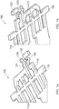
- a lead frame assembly 100 is illustrated in Figures 1a and 1b .
- the lead frame assembly 100 may further comprise one or more sets of leads 112, 116 extending from a first side thereof.
- a first set of leads 112 may be integrally connected to form a first connection point, or die connection portion, suitable for connection to a first contact terminal of a semiconductor die (not illustrated in Figures 1a and 1b ), such a source terminal.
- the leads 112 may be connected to each other and arranged to form a support member (not illustrated) wherein the support member may be arranged to contact and be supported by a die attach structure (not illustrated).
- a second lead 116 may be arranged to be connected to the support member, where the second lead 116 may be arranged to be connected to a further contact terminal of the semiconductor die, such as a gate terminal of the semiconductor die.
- a dam-bar 118 may be integrally formed with the leads and may extend orthogonally across the one or more leads 112, 116.
- the second lead 116 is substantially elongate and of generally of uniform thickness along its length.
- the second lead 116 includes a downwardly extending portion, or down stand 120, to facilitate connection of the second lead 116 to a metallisation terminal of the semiconductor die.
- the down stand 120 may be formed by locally increasing the thickness of the second lead 116 at the point where it contacts the terminal of the semiconductor die. In this way the down stand 120 has a height from the point where it will contact the semiconductor to the point where is joins the second lead 116.
- the down stand 120 may be formed by deforming the second lead 116 to include a double bend to form a U - shaped portion or V - shaped portion, at the point where it contacts the terminal of the semiconductor die.
- a hooking tab 122 is arranged at the end of the second lead 116 distal the support member 114 and adjacent to the down stand 120.
- the hooking tab 122 is configured and arranged such that a wire loop or hook of a wire pull test equipment may be looped around or under and thus mechanically engage with the hooking tab 122.
- the down stand 120 facilitates ease of engagement of the wire pull test equipment with the hooking tab 122, by ensuring that the hooking tab 122 is raised above and spaced apart from a top surface of the semiconductor die.
- the hooking tab 122 is arranged as an extension of the second lead 116 and may extend away from the second lead 116 in a direction substantially orthogonal to the second lead 116 as illustrated. Similarly, the hooking tab 122 may extend away from the second lead 116 along the same axis as the second lead 116. Likewise, the hooking tab 122 may extend away from the second lead 116 at any position intermediate the direction substantially orthogonal to the second lead 116 and the direction along the same axis as the second lead 116. In any case, the hooking tab 122 is arranged such that it extends in outward direction away from the second lead. In this way the hooking tab is arranged to extend at an angle of 0 degrees from the second lead 116 to substantially 90 degrees from the second lead 116. This allows for ease of access of the hooking tab and therefore ease of engagement with the wire loop of a wire pull test equipment.
- the hooking tab 122 may extend from the second lead 116 in any suitable direction.
- the hooking tab 122 should preferably have a length such that it does not extend outside the eventually moulded semiconductor device.
- the hooking tab 122 may be arranged so that it is contained within the finally packaged semiconductor device. In doing so the risk of a short circuit or leakage currents to the second lead 116 is minimised.
- the hooking tab 122 should preferably be arranged such that when viewed from above as in Figure 2 , it points away from the centre of the semiconductor die. In this way the risk of potential damage to the semiconductor die is minimised during the pull test procedure.
- the hooking tab 122 may be unitarily formed with the second lead 116 and may have the same thickness as the second lead 116 at the point where the hooking tab 122 meets the second lead 116.
- the hooking tab 122 may include a notch (not illustrated) formed on an its underside, to facilitate gripping of the wire pull test equipment.
- a hole (not illustrated) may be provided through the hooking tab 122 to allow for insertion of the wire pull test equipment to facilitate gripping of the wire pull test equipment thereon.
- the hooking tab 122 should preferably formed such that extends away from the end of the second lead 116, such that the down stand 120 is at a position intermediate the point where the second lead 116 intersects the dam-bar 118 and the hooking tab 122. In this way the pulling moment about the intersection of the second lead 116 and the dam-bar 118, acting a pivot point, is maximised.
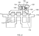
- Figure 2 illustrates a lead frame assembly as set out above mounted on a MOSFET semiconductor die 130, where the down stands 120, 126 of first and second leads contact respective gate and source terminals 132, 134 arranged on a top surface of the semiconductor die 130.
- processing of the semiconductor device continues by moulding the lead frame assembly 100 and the semiconductor die 130 and then trimming the leads along line A-A to form the final semiconductor device.
- the wire pull test equipment may be connected to the hooking tab 122 for testing the bond connection of the lead to the respective gate and source terminals 132, 134 of the semiconductor die 130.
- FIGS 1a, 1b and 2 illustrate a hooking tab 122 formed on the second lead 116, the gate lead in this example, the skilled person will also appreciate that a similar hooking tab 122 may also be arranged on another lead.
- the hooking tab may be formed on the source lead (first lead) or both the source lead and the gate lead.
- the first set of leads 112 may be formed to converge to a single lead were the single lead is configured as a source lead 124 for connection to a source terminal of the semiconductor die.
- the source lead 124 may also include a down stand 126, as described above, for contacting to a source terminal on a top surface of a semiconductor die.
- the source lead 124 including a hooking tab 122 should preferably have a length such that it does not extend outside the eventually moulded semiconductor device. In doing so the risk of a short circuit or leakage currents to the source lead 124 is minimised.
- the hooking tab 122 should preferably be arranged such that it points away from the semiconductor die. In this way the risk of potential damage to the semiconductor die is minimised during the pull test procedure.
- Figure 4 illustrates the arrangement of Figure 3 connected to a semiconductor die consistent with the discussion above in relation to Figure 2 .
- a wire loop or hook 402 of a wire pull test equipment looped under the hooking tab 122 of the gate lead 124.
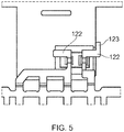
- Figure 5 illustrates a further example according to embodiments whereby the hooking tab 122 includes an extension portion 123.
- this extension portion By including this extension portion the pulling moment on the hooking tab 122 may be further increased when compared to the arrangement of Figure 2 , whilst ensuring that the hooking tab 122 and extension portion 123 do not extend outside the eventually moulded semiconductor device.
- the extension portion 123 should preferably be arranged such that when viewed from above as in Figure 2 , it points away from the centre of semiconductor die.
- Figure 5 illustrates the extension portion 123 arranged on the hooking tab 122 of the gate lead, following the above principles, the skilled person will appreciate that a similar extension portion could be included on the source lead.
- the first leads 112, 124 may form source connections to a source terminal on top side of the semiconductor die 106.
- the second leads 116 may form a gate connection to a gate terminal 118 also formed on the top side of the semiconductor die 106.
- the semiconductor die 106 may be a field effect transistor.
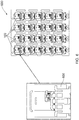
- FIG. 6 a matrix arrangement 600 of lead frame assemblies 100 according to embodiments as discussed above is illustrated.
- the matrix 600 is arranged as a 4 x 5 matrix, however the skilled will appreciate that any number of rows or columns may be included.
- the inset to Figure 6 illustrates an individual leadframe assembly 100 according to the above described arrangements and the matrix 600 illustrates the interconnected nature of matrix of individual leadframe assemblies.
- the hooking feature may be applied to one of more of a base clip, collector clip or emitter clip connections as appropriate.
- the semiconductor die is a bipolar junction transistor.
- the first leads 112 may form collector connections to a collector terminal 110 on the top side of a semiconductor die.
- the second lead 124 may form a base connection to a base terminal also formed on the top side of the semiconductor die 108.
Landscapes
- Lead Frames For Integrated Circuits (AREA)
Abstract
Description
- The present disclosure relates to a leadframe assembly for a semiconductor device. In particular the present disclosure relates a clip leadframe assembly for a semiconductor device and a matrix of such leadframe assemblies.
- For discrete semiconductor devices such as MOSFETs, it is possible to determine the reliability of source electrical connections to a semiconductor die metallisation using a DC test such as electrical drain source resistance measurements known as RDS testing. However, due to the presence of the insulating gate oxide it is not possible to use DC measurements to test the gate connections. Also, more generally, there are problems associated with RDS testing whereby an RDS test shows good electrical results but the mechanical bond is not well formed. For example, in the case of clip bonded electrical connections, the metal clip may be in contact with the die metallisation terminal and show good RDS characteristics, however the solder connection to the metallisation may be poor and thus potentially fail in cases where the connections undergo thermal expansion during reflow processes or during device operation. In such cases the connection may fail despite passing an RDS test.
- In semiconductor manufacturing a so-called bond shear testing is used to evaluate the quality of a wire bond connection from a device terminal to a contact on the semiconductor die. Such tests are used as quality tests to verify bond consistency and determine reliability of the bonds. According to recognised standards the aim of the test is to measure bond strengths, evaluate bond strength distributions, and/or determine compliance with specified bond strength requirements. The test may be destructive or non-destructive. In the case of destructive testing the wire is pulled until either the wire or the bond connection fails. In the case of non-destructive testing the bond is tested to determine the pulling force it can resist. Typically, prior to encapsulation of the semiconductor device a mechanical test hook is looped under the wire and the hook is then pulled with a certain force. The test may be carried out using a wire bond test machine or may be carried out manually by technicians or operators.
- In semiconductor devices, clip bonded packages are commonly used to make connections from a semiconductor die to external contacts of the device. Clip bonded packages have a number of advantages over conventional wire bonded packages. For example, clip bonded packages are typically used for mechanically robust and reliable electrical connections to and from the semiconductor die in automotive applications. For semiconductor devices using so-called clip packages, such as LFPAK, the above problems related to DC testing remain. Furthermore, with clip based packages it is difficult to insert the mechanical test hook under the source or gate clips due to close proximity of the clip to the semiconductor die. In addition, clip packages are typically arranged as an interconnected matrix, whereby each unit of the matrix corresponds to the clip connections for an individual semiconductor device.
- During reflow processing of the semiconductor device, the clip may become tilted or misaligned with a terminal of the semiconductor die, for example due to outgassing effects. It is desirable to test the reliability of misaligned clips to determine if the connection of the clip to the terminal of the die is reliable. It is also desirable to test all or a sample of such semiconductor devices, in particular when such device are used in safety critical applications such as automotive applications.
- Various example embodiments are directed to issues such as those addressed above and/or others which may become apparent from the following disclosure concerning leadframe assemblies for semiconductor devices. In certain example embodiments, aspects of the present disclosure involve the use of a leadframe assemblies that provide for simple reliability testing.
- According to an embodiment there is provided a leadframe assembly for a semiconductor device, the leadframe assembly comprising: a clip frame structure; the clip frame structure comprising: a die connection portion configured and arranged for contacting to one or more contact terminals on a top side of a semiconductor die; one or more electrical leads extending from the die connection portion at a first end, wherein the die connection portion comprises an hooking tab extending therefrom configured and arranged to engage with a wire loop of a wire pull test equipment.
- According to an embodiment there is provided a leadframe assembly for a semiconductor device, the leadframe assembly comprising: a clip frame structure; the clip frame structure comprising: a die connection portion configured and arranged for contacting to one or more contact terminals on a top side of a semiconductor die; one or more electrical leads extending from the die connection portion at a first end, wherein the die connection portion comprises an hooking tab extending therefrom configured and arranged to be engaged with a wire loop of a wire pull test equipment.
- The die connection portion may be substantially elongate and comprise a downward extending portion at a point where the die connection portion is arranged to contact a terminal of the semiconductor die.
- The downward extending portion may raise the hooking tab corresponding to the height of the downward extending portion.
- The hooking tab may be arranged to extend at an angle of substantially 0 degrees from the die connection portion to substantially 90 degrees from the die connection portion.
- The hooking tab may arranged such that it extends substantially orthogonally from the die connection portion.
- The hooking tab may include an extension portion extending therefrom configured and arranged to engage with a wire loop of a wire pull test equipment. The hooking tab may integrally formed with die connection portion. The extension portion may be integrally formed with the hooking tab.
- The die connection portion may be a gate connection to the semiconductor die. The die connection portion may be a source connection to the semiconductor die.
- The lead frame assembly according to an embodiment may further comprising a dam bar extending orthogonally across the one or more electrical leads.
- There is also provided a lead frame matrix wherein a unit of the matrix comprises a lead frame assembly according to embodiments. Adjoining units of the matrix are connected by respective dam bars of each lead frame assembly.
- So that the manner in which the features of the present disclosure can be understood in detail, a more particular description is made with reference to embodiments, some of which are illustrated in the appended figures. It is to be noted, however, that the appended figures illustrate only typical embodiments and are therefore not to be considered limiting of its scope. The figures are for facilitating an understanding of the disclosure and thus are not necessarily drawn to scale. Advantages of the subject matter claimed will become apparent to those skilled in the art upon reading this description in conjunction with the accompanying figures, in which like reference numerals have been used to designate like elements, and in which:
-
Figure 1a is a top side perspective view of a leadframe assembly according to embodiments; -
Figure 1b is a bottom side perspective view of a leadframe assembly according to embodiments; -
Figure 2 is a top side view of the leadframe assembly connected to a semiconductor die; -
Figure 3 is a top side perspective view of a leadframe assembly according to embodiments; -
Figure 4 is a top side view of the leadframe assembly according to embodiments connected to a semiconductor die; -
Figure 5 is a top side view of the leadframe assembly connected to a semiconductor die; and -
Figure 6 is a top side view of a matrix of leadframe assemblies according to embodiments. - A
lead frame assembly 100 according to an embodiment is illustrated inFigures 1a and 1b . By way of general overview, thelead frame assembly 100 may further comprise one or more sets ofleads leads 112 may be integrally connected to form a first connection point, or die connection portion, suitable for connection to a first contact terminal of a semiconductor die (not illustrated inFigures 1a and 1b ), such a source terminal. At a second end, distal the first end, theleads 112 may be connected to each other and arranged to form a support member (not illustrated) wherein the support member may be arranged to contact and be supported by a die attach structure (not illustrated). Asecond lead 116 may be arranged to be connected to the support member, where thesecond lead 116 may be arranged to be connected to a further contact terminal of the semiconductor die, such as a gate terminal of the semiconductor die. Optionally, a dam-bar 118 may be integrally formed with the leads and may extend orthogonally across the one ormore leads - The
second lead 116 is substantially elongate and of generally of uniform thickness along its length. However, thesecond lead 116 includes a downwardly extending portion, or downstand 120, to facilitate connection of thesecond lead 116 to a metallisation terminal of the semiconductor die. The downstand 120 may be formed by locally increasing the thickness of thesecond lead 116 at the point where it contacts the terminal of the semiconductor die. In this way thedown stand 120 has a height from the point where it will contact the semiconductor to the point where is joins thesecond lead 116. Alternatively, thedown stand 120 may be formed by deforming thesecond lead 116 to include a double bend to form a U - shaped portion or V - shaped portion, at the point where it contacts the terminal of the semiconductor die. - A hooking
tab 122 is arranged at the end of thesecond lead 116 distal the support member 114 and adjacent to thedown stand 120. The hookingtab 122 is configured and arranged such that a wire loop or hook of a wire pull test equipment may be looped around or under and thus mechanically engage with the hookingtab 122. The downstand 120 facilitates ease of engagement of the wire pull test equipment with the hookingtab 122, by ensuring that the hookingtab 122 is raised above and spaced apart from a top surface of the semiconductor die. - The hooking
tab 122 is arranged as an extension of thesecond lead 116 and may extend away from thesecond lead 116 in a direction substantially orthogonal to thesecond lead 116 as illustrated. Similarly, the hookingtab 122 may extend away from thesecond lead 116 along the same axis as thesecond lead 116. Likewise, the hookingtab 122 may extend away from thesecond lead 116 at any position intermediate the direction substantially orthogonal to thesecond lead 116 and the direction along the same axis as thesecond lead 116. In any case, the hookingtab 122 is arranged such that it extends in outward direction away from the second lead. In this way the hooking tab is arranged to extend at an angle of 0 degrees from thesecond lead 116 to substantially 90 degrees from thesecond lead 116. This allows for ease of access of the hooking tab and therefore ease of engagement with the wire loop of a wire pull test equipment. - Based on the present disclosure, the skilled person will appreciate that the hooking
tab 122 may extend from thesecond lead 116 in any suitable direction. The hookingtab 122 should preferably have a length such that it does not extend outside the eventually moulded semiconductor device. In other words, the hookingtab 122 may be arranged so that it is contained within the finally packaged semiconductor device. In doing so the risk of a short circuit or leakage currents to thesecond lead 116 is minimised. In addition, the hookingtab 122 should preferably be arranged such that when viewed from above as inFigure 2 , it points away from the centre of the semiconductor die. In this way the risk of potential damage to the semiconductor die is minimised during the pull test procedure. - The hooking
tab 122 may be unitarily formed with thesecond lead 116 and may have the same thickness as thesecond lead 116 at the point where the hookingtab 122 meets thesecond lead 116. Optionally, the hookingtab 122 may include a notch (not illustrated) formed on an its underside, to facilitate gripping of the wire pull test equipment. Alternatively, a hole (not illustrated) may be provided through the hookingtab 122 to allow for insertion of the wire pull test equipment to facilitate gripping of the wire pull test equipment thereon. - The hooking
tab 122 should preferably formed such that extends away from the end of thesecond lead 116, such that thedown stand 120 is at a position intermediate the point where thesecond lead 116 intersects the dam-bar 118 and the hookingtab 122. In this way the pulling moment about the intersection of thesecond lead 116 and the dam-bar 118, acting a pivot point, is maximised. -
Figure 2 , illustrates a lead frame assembly as set out above mounted on a MOSFET semiconductor die 130, where the down stands 120, 126 of first and second leads contact respective gate andsource terminals lead frame assembly 100 on the semiconductor die 130, processing of the semiconductor device continues by moulding thelead frame assembly 100 and the semiconductor die 130 and then trimming the leads along line A-A to form the final semiconductor device. Prior to moulding of device the wire pull test equipment may be connected to the hookingtab 122 for testing the bond connection of the lead to the respective gate andsource terminals - Whilst
Figures 1a, 1b and2 , illustrate a hookingtab 122 formed on thesecond lead 116, the gate lead in this example, the skilled person will also appreciate that a similar hookingtab 122 may also be arranged on another lead. For example as well as the hookingtab 122 being formed on the gate lead (second lead), the hooking tab may be formed on the source lead (first lead) or both the source lead and the gate lead. As illustrated inFigure 3 , the first set ofleads 112, may be formed to converge to a single lead were the single lead is configured as asource lead 124 for connection to a source terminal of the semiconductor die. The source lead 124 may also include adown stand 126, as described above, for contacting to a source terminal on a top surface of a semiconductor die. Following the principles discussed above with respect toFigures 1a, 1b and2 , the source lead 124 including a hookingtab 122 should preferably have a length such that it does not extend outside the eventually moulded semiconductor device. In doing so the risk of a short circuit or leakage currents to the source lead 124 is minimised. In addition, when viewed from above as inFigure 4 , the hookingtab 122 should preferably be arranged such that it points away from the semiconductor die. In this way the risk of potential damage to the semiconductor die is minimised during the pull test procedure.Figure 4 illustrates the arrangement ofFigure 3 connected to a semiconductor die consistent with the discussion above in relation toFigure 2 . A wire loop or hook 402 of a wire pull test equipment looped under the hookingtab 122 of thegate lead 124. - Whilst the
Figures 3 andFigure 4 , show hookingtab 122 located on both the source lead and gate lead, the skilled person will appreciate that one or other of the hooking features may be omitted as required by the application of thelead frame assembly 100. -
Figure 5 illustrates a further example according to embodiments whereby the hookingtab 122 includes anextension portion 123. By including this extension portion the pulling moment on the hookingtab 122 may be further increased when compared to the arrangement ofFigure 2 , whilst ensuring that the hookingtab 122 andextension portion 123 do not extend outside the eventually moulded semiconductor device. Based on the above discussion with respect to the relative orientation of the hooking tab with respect to the leads, theextension portion 123 should preferably be arranged such that when viewed from above as inFigure 2 , it points away from the centre of semiconductor die. - Whilst
Figure 5 illustrates theextension portion 123 arranged on the hookingtab 122 of the gate lead, following the above principles, the skilled person will appreciate that a similar extension portion could be included on the source lead. - According to embodiments, the first leads 112, 124 may form source connections to a source terminal on top side of the semiconductor die 106. The second leads 116 may form a gate connection to a
gate terminal 118 also formed on the top side of the semiconductor die 106. In this regard the semiconductor die 106 may be a field effect transistor. - Turning now to
Figure 6 amatrix arrangement 600 oflead frame assemblies 100 according to embodiments as discussed above is illustrated. In the example ofFigure 6 thematrix 600 is arranged as a 4 x 5 matrix, however the skilled will appreciate that any number of rows or columns may be included. The inset toFigure 6 illustrates anindividual leadframe assembly 100 according to the above described arrangements and thematrix 600 illustrates the interconnected nature of matrix of individual leadframe assemblies. - In addition, whilst embodiments of the disclosure are discussed in relation to MOSFET semiconductor devices and specifically source and gate clip based leads, they are not so limited. The skilled person will appreciate that the present disclosure is also relevant to clip based leadframe assemblies of any semiconductor device and in particular discrete devices such as for example bipolar transistors. In the example of bipolar transistors the hooking feature may be applied to one of more of a base clip, collector clip or emitter clip connections as appropriate. Where the semiconductor die is a bipolar junction transistor. The first leads 112 may form collector connections to a collector terminal 110 on the top side of a semiconductor die. The
second lead 124 may form a base connection to a base terminal also formed on the top side of the semiconductor die 108. - Particular and preferred aspects of the invention are set out in the accompanying independent claims. Combinations of features from the dependent and/or independent claims may be combined as appropriate and not merely as set out in the claims.
- The scope of the present disclosure includes any novel feature or combination of features disclosed therein either explicitly or implicitly or any generalisation thereof irrespective of whether or not it relates to the claimed invention or mitigate against any or all of the problems addressed by the present invention. The applicant hereby gives notice that new claims may be formulated to such features during prosecution of this application or of any such further application derived therefrom. In particular, with reference to the appended claims, features from dependent claims may be combined with those of the independent claims and features from respective independent claims may be combined in any appropriate manner and not merely in specific combinations enumerated in the claims.
- Features which are described in the context of separate embodiments may also be provided in combination in a single embodiment. Conversely, various features which are, for brevity, described in the context of a single embodiment, may also be provided separately or in any suitable sub combination.
- Term "comprising" does not exclude other elements or steps, the term "a" or "an" does not exclude a plurality. Reference signs in the claims shall not be construed as limiting the scope of the claims.
Claims (13)
- A leadframe assembly for a semiconductor device, the leadframe assembly comprising:a clip frame structure;the clip frame structure comprising:a die connection portion configured and arranged for contacting to one or more contact terminals on a top side of a semiconductor die;one or more electrical leads extending from the die connection portion at a first end,wherein the die connection portion comprises an hooking tab extending therefrom configured and arranged to be engaged with a wire loop of a wire pull test equipment.
- The lead frame assembly of claim 1, wherein the die connection portion is substantially elongate and comprises a downward extending portion at a point where the die connection portion is arranged to contact a terminal of the semiconductor die.
- The lead frame assembly of claim 2, wherein the downward extending portion raises the hooking tab corresponding to the height of the downward extending portion.
- The lead frame assembly of claims 1 to 3, wherein the hooking tab is arranged to extend at an angle of substantially 0 degrees from the die connection portion to substantially 90 degrees from the die connection portion.
- The lead frame assembly of claims 1 to 3, wherein the hooking tab is arranged such that it extends substantially orthogonally from the die connection portion.
- The lead frame assembly of any preceding claim wherein the hooking tab includes an extension portion extending therefrom configured and arranged to engage with a wire loop of a wire pull test equipment.
- The lead frame assembly of any preceding claim, wherein the hooking tab is integrally formed with die connection portion.
- The lead frame assembly of any one or more of claims 1 to 7, wherein the extension portion and is integrally formed with the hooking tab.
- The lead frame assembly of any preceding claim, wherein the die connection portion is a gate connection to the semiconductor die.
- The lead frame assembly of claims 1 to 6, wherein the die connection portion is a source connection to the semiconductor die.
- The lead frame assembly of any preceding claim, further comprising a dam bar extending orthogonally across the one or more electrical leads.
- A matrix of lead frames wherein a unit of the matrix comprises a lead frame assemblie according to any preceding claim.
- The matrix of lead frames where adjoining units of the matrix are connected by respective dam bars of each lead frame assembly.
Priority Applications (3)
| Application Number | Priority Date | Filing Date | Title |
|---|---|---|---|
| EP18212898.3A EP3671829B1 (en) | 2018-12-17 | 2018-12-17 | Leadframe assembly for a semiconductor device |
| US16/715,385 US10714413B2 (en) | 2018-12-17 | 2019-12-16 | Leadframe assembly for a semiconductor device |
| CN201911291444.4A CN111326493B (en) | 2018-12-17 | 2019-12-16 | Lead frame assembly for semiconductor device |
Applications Claiming Priority (1)
| Application Number | Priority Date | Filing Date | Title |
|---|---|---|---|
| EP18212898.3A EP3671829B1 (en) | 2018-12-17 | 2018-12-17 | Leadframe assembly for a semiconductor device |
Publications (2)
| Publication Number | Publication Date |
|---|---|
| EP3671829A1 true EP3671829A1 (en) | 2020-06-24 |
| EP3671829B1 EP3671829B1 (en) | 2023-09-27 |
Family
ID=64755125
Family Applications (1)
| Application Number | Title | Priority Date | Filing Date |
|---|---|---|---|
| EP18212898.3A Active EP3671829B1 (en) | 2018-12-17 | 2018-12-17 | Leadframe assembly for a semiconductor device |
Country Status (3)
| Country | Link |
|---|---|
| US (1) | US10714413B2 (en) |
| EP (1) | EP3671829B1 (en) |
| CN (1) | CN111326493B (en) |
Citations (5)
| Publication number | Priority date | Publication date | Assignee | Title |
|---|---|---|---|---|
| US4994412A (en) * | 1990-02-09 | 1991-02-19 | Motorola Inc. | Self-centering electrode for power devices |
| US5110761A (en) * | 1988-09-09 | 1992-05-05 | Motorola, Inc. | Formed top contact for non-flat semiconductor devices |
| US20090218673A1 (en) * | 2005-09-13 | 2009-09-03 | Ming Sun | Semiconductor package having a bridge plate connection |
| EP2930747A1 (en) * | 2014-04-07 | 2015-10-14 | Nxp B.V. | Lead for connection to a semiconductor device |
| EP3336881A1 (en) * | 2016-12-19 | 2018-06-20 | Nexperia B.V. | Semiconductor device and method with clip arrangement in ic package |
Family Cites Families (6)
| Publication number | Priority date | Publication date | Assignee | Title |
|---|---|---|---|---|
| US6204074B1 (en) * | 1995-01-09 | 2001-03-20 | International Business Machines Corporation | Chip design process for wire bond and flip-chip package |
| JPH09274065A (en) * | 1996-04-03 | 1997-10-21 | Sumitomo Electric Ind Ltd | Semiconductor device |
| JP4705881B2 (en) * | 2006-05-09 | 2011-06-22 | パナソニック株式会社 | Lead frame and semiconductor device using the same |
| JP5220714B2 (en) * | 2009-09-18 | 2013-06-26 | セイコーインスツル株式会社 | Resin-sealed semiconductor device and manufacturing method thereof |
| JP5823798B2 (en) * | 2011-09-29 | 2015-11-25 | ルネサスエレクトロニクス株式会社 | Semiconductor device |
| JP6451117B2 (en) * | 2014-04-01 | 2019-01-16 | 富士電機株式会社 | Semiconductor device manufacturing method and semiconductor device |
-
2018
- 2018-12-17 EP EP18212898.3A patent/EP3671829B1/en active Active
-
2019
- 2019-12-16 CN CN201911291444.4A patent/CN111326493B/en active Active
- 2019-12-16 US US16/715,385 patent/US10714413B2/en active Active
Patent Citations (5)
| Publication number | Priority date | Publication date | Assignee | Title |
|---|---|---|---|---|
| US5110761A (en) * | 1988-09-09 | 1992-05-05 | Motorola, Inc. | Formed top contact for non-flat semiconductor devices |
| US4994412A (en) * | 1990-02-09 | 1991-02-19 | Motorola Inc. | Self-centering electrode for power devices |
| US20090218673A1 (en) * | 2005-09-13 | 2009-09-03 | Ming Sun | Semiconductor package having a bridge plate connection |
| EP2930747A1 (en) * | 2014-04-07 | 2015-10-14 | Nxp B.V. | Lead for connection to a semiconductor device |
| EP3336881A1 (en) * | 2016-12-19 | 2018-06-20 | Nexperia B.V. | Semiconductor device and method with clip arrangement in ic package |
Also Published As
| Publication number | Publication date |
|---|---|
| CN111326493B (en) | 2024-09-13 |
| US10714413B2 (en) | 2020-07-14 |
| US20200194354A1 (en) | 2020-06-18 |
| EP3671829B1 (en) | 2023-09-27 |
| CN111326493A (en) | 2020-06-23 |
Similar Documents
| Publication | Publication Date | Title |
|---|---|---|
| US9812384B2 (en) | Semiconductor device having compliant and crack-arresting interconnect structure | |
| US5302891A (en) | Discrete die burn-in for non-packaged die | |
| US11973009B2 (en) | Lead frame assembly for a semiconductor device | |
| US8384206B2 (en) | Semiconductor package | |
| US5574383A (en) | IC tester and measuring method | |
| US6854637B2 (en) | Wirebonding insulated wire | |
| US20050127935A1 (en) | Semiconductor device tester | |
| US12347751B2 (en) | Semiconductor device and a method of manufacture | |
| US10714413B2 (en) | Leadframe assembly for a semiconductor device | |
| US6220102B1 (en) | Die-shear test fixture apparatus | |
| US20180261567A1 (en) | Window Clamp | |
| US9153518B2 (en) | Molded semiconductor package with pluggable lead | |
| US20190204380A1 (en) | Lead guides having a recessed face | |
| CN222233606U (en) | Decapsulation lead frame fixture and decapsulation test equipment | |
| US6998860B1 (en) | Method for burn-in testing semiconductor dice | |
| KR20120120595A (en) | Contact pin with multicontact point and the socket for test of semiconductor package comprising the same | |
| JPH05297020A (en) | Probe assembly | |
| JP2634286B2 (en) | Handler device for testing electrical characteristics of semiconductor devices | |
| JP5126009B2 (en) | Test method, test apparatus and semiconductor device manufacturing method | |
| US6140212A (en) | Semiconductor device and method therefor | |
| JP2026513663A (en) | Conductive connectors, power semiconductor modules, and methods for manufacturing conductive connectors | |
| KR19980027598U (en) | Conductive Sheets for Lead Contacts for Semiconductor Package Testing | |
| JP2613233B2 (en) | Aging method for semiconductor device | |
| JPH09274065A (en) | Semiconductor device | |
| JPH06334072A (en) | Kelvin contact type socket |
Legal Events
| Date | Code | Title | Description |
|---|---|---|---|
| PUAI | Public reference made under article 153(3) epc to a published international application that has entered the european phase |
Free format text: ORIGINAL CODE: 0009012 |
|
| STAA | Information on the status of an ep patent application or granted ep patent |
Free format text: STATUS: THE APPLICATION HAS BEEN PUBLISHED |
|
| AK | Designated contracting states |
Kind code of ref document: A1 Designated state(s): AL AT BE BG CH CY CZ DE DK EE ES FI FR GB GR HR HU IE IS IT LI LT LU LV MC MK MT NL NO PL PT RO RS SE SI SK SM TR |
|
| AX | Request for extension of the european patent |
Extension state: BA ME |
|
| STAA | Information on the status of an ep patent application or granted ep patent |
Free format text: STATUS: REQUEST FOR EXAMINATION WAS MADE |
|
| 17P | Request for examination filed |
Effective date: 20201224 |
|
| RBV | Designated contracting states (corrected) |
Designated state(s): AL AT BE BG CH CY CZ DE DK EE ES FI FR GB GR HR HU IE IS IT LI LT LU LV MC MK MT NL NO PL PT RO RS SE SI SK SM TR |
|
| STAA | Information on the status of an ep patent application or granted ep patent |
Free format text: STATUS: EXAMINATION IS IN PROGRESS |
|
| 17Q | First examination report despatched |
Effective date: 20210423 |
|
| GRAP | Despatch of communication of intention to grant a patent |
Free format text: ORIGINAL CODE: EPIDOSNIGR1 |
|
| STAA | Information on the status of an ep patent application or granted ep patent |
Free format text: STATUS: GRANT OF PATENT IS INTENDED |
|
| INTG | Intention to grant announced |
Effective date: 20230509 |
|
| GRAS | Grant fee paid |
Free format text: ORIGINAL CODE: EPIDOSNIGR3 |
|
| GRAA | (expected) grant |
Free format text: ORIGINAL CODE: 0009210 |
|
| STAA | Information on the status of an ep patent application or granted ep patent |
Free format text: STATUS: THE PATENT HAS BEEN GRANTED |
|
| AK | Designated contracting states |
Kind code of ref document: B1 Designated state(s): AL AT BE BG CH CY CZ DE DK EE ES FI FR GB GR HR HU IE IS IT LI LT LU LV MC MK MT NL NO PL PT RO RS SE SI SK SM TR |
|
| REG | Reference to a national code |
Ref country code: GB Ref legal event code: FG4D |
|
| REG | Reference to a national code |
Ref country code: CH Ref legal event code: EP |
|
| REG | Reference to a national code |
Ref country code: DE Ref legal event code: R096 Ref document number: 602018058198 Country of ref document: DE |
|
| REG | Reference to a national code |
Ref country code: IE Ref legal event code: FG4D |
|
| REG | Reference to a national code |
Ref country code: LT Ref legal event code: MG9D |
|
| PG25 | Lapsed in a contracting state [announced via postgrant information from national office to epo] |
Ref country code: GR Free format text: LAPSE BECAUSE OF FAILURE TO SUBMIT A TRANSLATION OF THE DESCRIPTION OR TO PAY THE FEE WITHIN THE PRESCRIBED TIME-LIMIT Effective date: 20231228 |
|
| PG25 | Lapsed in a contracting state [announced via postgrant information from national office to epo] |
Ref country code: SE Free format text: LAPSE BECAUSE OF FAILURE TO SUBMIT A TRANSLATION OF THE DESCRIPTION OR TO PAY THE FEE WITHIN THE PRESCRIBED TIME-LIMIT Effective date: 20230927 Ref country code: RS Free format text: LAPSE BECAUSE OF FAILURE TO SUBMIT A TRANSLATION OF THE DESCRIPTION OR TO PAY THE FEE WITHIN THE PRESCRIBED TIME-LIMIT Effective date: 20230927 Ref country code: NO Free format text: LAPSE BECAUSE OF FAILURE TO SUBMIT A TRANSLATION OF THE DESCRIPTION OR TO PAY THE FEE WITHIN THE PRESCRIBED TIME-LIMIT Effective date: 20231227 Ref country code: LV Free format text: LAPSE BECAUSE OF FAILURE TO SUBMIT A TRANSLATION OF THE DESCRIPTION OR TO PAY THE FEE WITHIN THE PRESCRIBED TIME-LIMIT Effective date: 20230927 Ref country code: LT Free format text: LAPSE BECAUSE OF FAILURE TO SUBMIT A TRANSLATION OF THE DESCRIPTION OR TO PAY THE FEE WITHIN THE PRESCRIBED TIME-LIMIT Effective date: 20230927 Ref country code: HR Free format text: LAPSE BECAUSE OF FAILURE TO SUBMIT A TRANSLATION OF THE DESCRIPTION OR TO PAY THE FEE WITHIN THE PRESCRIBED TIME-LIMIT Effective date: 20230927 Ref country code: GR Free format text: LAPSE BECAUSE OF FAILURE TO SUBMIT A TRANSLATION OF THE DESCRIPTION OR TO PAY THE FEE WITHIN THE PRESCRIBED TIME-LIMIT Effective date: 20231228 Ref country code: FI Free format text: LAPSE BECAUSE OF FAILURE TO SUBMIT A TRANSLATION OF THE DESCRIPTION OR TO PAY THE FEE WITHIN THE PRESCRIBED TIME-LIMIT Effective date: 20230927 |
|
| REG | Reference to a national code |
Ref country code: NL Ref legal event code: MP Effective date: 20230927 |
|
| REG | Reference to a national code |
Ref country code: AT Ref legal event code: MK05 Ref document number: 1616293 Country of ref document: AT Kind code of ref document: T Effective date: 20230927 |
|
| PG25 | Lapsed in a contracting state [announced via postgrant information from national office to epo] |
Ref country code: NL Free format text: LAPSE BECAUSE OF FAILURE TO SUBMIT A TRANSLATION OF THE DESCRIPTION OR TO PAY THE FEE WITHIN THE PRESCRIBED TIME-LIMIT Effective date: 20230927 |
|
| PG25 | Lapsed in a contracting state [announced via postgrant information from national office to epo] |
Ref country code: IS Free format text: LAPSE BECAUSE OF FAILURE TO SUBMIT A TRANSLATION OF THE DESCRIPTION OR TO PAY THE FEE WITHIN THE PRESCRIBED TIME-LIMIT Effective date: 20240127 |
|
| PG25 | Lapsed in a contracting state [announced via postgrant information from national office to epo] |
Ref country code: AT Free format text: LAPSE BECAUSE OF FAILURE TO SUBMIT A TRANSLATION OF THE DESCRIPTION OR TO PAY THE FEE WITHIN THE PRESCRIBED TIME-LIMIT Effective date: 20230927 |
|
| PG25 | Lapsed in a contracting state [announced via postgrant information from national office to epo] |
Ref country code: ES Free format text: LAPSE BECAUSE OF FAILURE TO SUBMIT A TRANSLATION OF THE DESCRIPTION OR TO PAY THE FEE WITHIN THE PRESCRIBED TIME-LIMIT Effective date: 20230927 |
|
| PG25 | Lapsed in a contracting state [announced via postgrant information from national office to epo] |
Ref country code: SM Free format text: LAPSE BECAUSE OF FAILURE TO SUBMIT A TRANSLATION OF THE DESCRIPTION OR TO PAY THE FEE WITHIN THE PRESCRIBED TIME-LIMIT Effective date: 20230927 Ref country code: RO Free format text: LAPSE BECAUSE OF FAILURE TO SUBMIT A TRANSLATION OF THE DESCRIPTION OR TO PAY THE FEE WITHIN THE PRESCRIBED TIME-LIMIT Effective date: 20230927 Ref country code: IS Free format text: LAPSE BECAUSE OF FAILURE TO SUBMIT A TRANSLATION OF THE DESCRIPTION OR TO PAY THE FEE WITHIN THE PRESCRIBED TIME-LIMIT Effective date: 20240127 Ref country code: ES Free format text: LAPSE BECAUSE OF FAILURE TO SUBMIT A TRANSLATION OF THE DESCRIPTION OR TO PAY THE FEE WITHIN THE PRESCRIBED TIME-LIMIT Effective date: 20230927 Ref country code: EE Free format text: LAPSE BECAUSE OF FAILURE TO SUBMIT A TRANSLATION OF THE DESCRIPTION OR TO PAY THE FEE WITHIN THE PRESCRIBED TIME-LIMIT Effective date: 20230927 Ref country code: CZ Free format text: LAPSE BECAUSE OF FAILURE TO SUBMIT A TRANSLATION OF THE DESCRIPTION OR TO PAY THE FEE WITHIN THE PRESCRIBED TIME-LIMIT Effective date: 20230927 Ref country code: AT Free format text: LAPSE BECAUSE OF FAILURE TO SUBMIT A TRANSLATION OF THE DESCRIPTION OR TO PAY THE FEE WITHIN THE PRESCRIBED TIME-LIMIT Effective date: 20230927 Ref country code: PT Free format text: LAPSE BECAUSE OF FAILURE TO SUBMIT A TRANSLATION OF THE DESCRIPTION OR TO PAY THE FEE WITHIN THE PRESCRIBED TIME-LIMIT Effective date: 20240129 Ref country code: SK Free format text: LAPSE BECAUSE OF FAILURE TO SUBMIT A TRANSLATION OF THE DESCRIPTION OR TO PAY THE FEE WITHIN THE PRESCRIBED TIME-LIMIT Effective date: 20230927 |
|
| PG25 | Lapsed in a contracting state [announced via postgrant information from national office to epo] |
Ref country code: PL Free format text: LAPSE BECAUSE OF FAILURE TO SUBMIT A TRANSLATION OF THE DESCRIPTION OR TO PAY THE FEE WITHIN THE PRESCRIBED TIME-LIMIT Effective date: 20230927 Ref country code: IT Free format text: LAPSE BECAUSE OF FAILURE TO SUBMIT A TRANSLATION OF THE DESCRIPTION OR TO PAY THE FEE WITHIN THE PRESCRIBED TIME-LIMIT Effective date: 20230927 |
|
| REG | Reference to a national code |
Ref country code: DE Ref legal event code: R097 Ref document number: 602018058198 Country of ref document: DE |
|
| PG25 | Lapsed in a contracting state [announced via postgrant information from national office to epo] |
Ref country code: DK Free format text: LAPSE BECAUSE OF FAILURE TO SUBMIT A TRANSLATION OF THE DESCRIPTION OR TO PAY THE FEE WITHIN THE PRESCRIBED TIME-LIMIT Effective date: 20230927 |
|
| PG25 | Lapsed in a contracting state [announced via postgrant information from national office to epo] |
Ref country code: DK Free format text: LAPSE BECAUSE OF FAILURE TO SUBMIT A TRANSLATION OF THE DESCRIPTION OR TO PAY THE FEE WITHIN THE PRESCRIBED TIME-LIMIT Effective date: 20230927 |
|
| REG | Reference to a national code |
Ref country code: CH Ref legal event code: PL |
|
| PLBE | No opposition filed within time limit |
Free format text: ORIGINAL CODE: 0009261 |
|
| STAA | Information on the status of an ep patent application or granted ep patent |
Free format text: STATUS: NO OPPOSITION FILED WITHIN TIME LIMIT |
|
| PG25 | Lapsed in a contracting state [announced via postgrant information from national office to epo] |
Ref country code: LU Free format text: LAPSE BECAUSE OF NON-PAYMENT OF DUE FEES Effective date: 20231217 |
|
| PG25 | Lapsed in a contracting state [announced via postgrant information from national office to epo] |
Ref country code: MC Free format text: LAPSE BECAUSE OF FAILURE TO SUBMIT A TRANSLATION OF THE DESCRIPTION OR TO PAY THE FEE WITHIN THE PRESCRIBED TIME-LIMIT Effective date: 20230927 |
|
| GBPC | Gb: european patent ceased through non-payment of renewal fee |
Effective date: 20231227 |
|
| REG | Reference to a national code |
Ref country code: BE Ref legal event code: MM Effective date: 20231231 |
|
| PG25 | Lapsed in a contracting state [announced via postgrant information from national office to epo] |
Ref country code: MC Free format text: LAPSE BECAUSE OF FAILURE TO SUBMIT A TRANSLATION OF THE DESCRIPTION OR TO PAY THE FEE WITHIN THE PRESCRIBED TIME-LIMIT Effective date: 20230927 Ref country code: LU Free format text: LAPSE BECAUSE OF NON-PAYMENT OF DUE FEES Effective date: 20231217 |
|
| 26N | No opposition filed |
Effective date: 20240628 |
|
| REG | Reference to a national code |
Ref country code: IE Ref legal event code: MM4A |
|
| PG25 | Lapsed in a contracting state [announced via postgrant information from national office to epo] |
Ref country code: IE Free format text: LAPSE BECAUSE OF NON-PAYMENT OF DUE FEES Effective date: 20231217 |
|
| PG25 | Lapsed in a contracting state [announced via postgrant information from national office to epo] |
Ref country code: GB Free format text: LAPSE BECAUSE OF NON-PAYMENT OF DUE FEES Effective date: 20231227 |
|
| PG25 | Lapsed in a contracting state [announced via postgrant information from national office to epo] |
Ref country code: BE Free format text: LAPSE BECAUSE OF NON-PAYMENT OF DUE FEES Effective date: 20231231 |
|
| PG25 | Lapsed in a contracting state [announced via postgrant information from national office to epo] |
Ref country code: FR Free format text: LAPSE BECAUSE OF NON-PAYMENT OF DUE FEES Effective date: 20231231 |
|
| PG25 | Lapsed in a contracting state [announced via postgrant information from national office to epo] |
Ref country code: CH Free format text: LAPSE BECAUSE OF NON-PAYMENT OF DUE FEES Effective date: 20231231 |
|
| PG25 | Lapsed in a contracting state [announced via postgrant information from national office to epo] |
Ref country code: SI Free format text: LAPSE BECAUSE OF FAILURE TO SUBMIT A TRANSLATION OF THE DESCRIPTION OR TO PAY THE FEE WITHIN THE PRESCRIBED TIME-LIMIT Effective date: 20230927 |
|
| PG25 | Lapsed in a contracting state [announced via postgrant information from national office to epo] |
Ref country code: SI Free format text: LAPSE BECAUSE OF FAILURE TO SUBMIT A TRANSLATION OF THE DESCRIPTION OR TO PAY THE FEE WITHIN THE PRESCRIBED TIME-LIMIT Effective date: 20230927 Ref country code: IE Free format text: LAPSE BECAUSE OF NON-PAYMENT OF DUE FEES Effective date: 20231217 Ref country code: GB Free format text: LAPSE BECAUSE OF NON-PAYMENT OF DUE FEES Effective date: 20231227 Ref country code: FR Free format text: LAPSE BECAUSE OF NON-PAYMENT OF DUE FEES Effective date: 20231231 Ref country code: CH Free format text: LAPSE BECAUSE OF NON-PAYMENT OF DUE FEES Effective date: 20231231 Ref country code: BE Free format text: LAPSE BECAUSE OF NON-PAYMENT OF DUE FEES Effective date: 20231231 |
|
| PG25 | Lapsed in a contracting state [announced via postgrant information from national office to epo] |
Ref country code: BG Free format text: LAPSE BECAUSE OF FAILURE TO SUBMIT A TRANSLATION OF THE DESCRIPTION OR TO PAY THE FEE WITHIN THE PRESCRIBED TIME-LIMIT Effective date: 20230927 |
|
| PG25 | Lapsed in a contracting state [announced via postgrant information from national office to epo] |
Ref country code: BG Free format text: LAPSE BECAUSE OF FAILURE TO SUBMIT A TRANSLATION OF THE DESCRIPTION OR TO PAY THE FEE WITHIN THE PRESCRIBED TIME-LIMIT Effective date: 20230927 |
|
| PG25 | Lapsed in a contracting state [announced via postgrant information from national office to epo] |
Ref country code: CY Free format text: LAPSE BECAUSE OF FAILURE TO SUBMIT A TRANSLATION OF THE DESCRIPTION OR TO PAY THE FEE WITHIN THE PRESCRIBED TIME-LIMIT; INVALID AB INITIO Effective date: 20181217 |
|
| PG25 | Lapsed in a contracting state [announced via postgrant information from national office to epo] |
Ref country code: HU Free format text: LAPSE BECAUSE OF FAILURE TO SUBMIT A TRANSLATION OF THE DESCRIPTION OR TO PAY THE FEE WITHIN THE PRESCRIBED TIME-LIMIT; INVALID AB INITIO Effective date: 20181217 |
|
| REG | Reference to a national code |
Ref country code: DE Ref legal event code: R079 Ref document number: 602018058198 Country of ref document: DE Free format text: PREVIOUS MAIN CLASS: H01L0023495000 Ipc: H10W0070400000 |
|
| PG25 | Lapsed in a contracting state [announced via postgrant information from national office to epo] |
Ref country code: TR Free format text: LAPSE BECAUSE OF FAILURE TO SUBMIT A TRANSLATION OF THE DESCRIPTION OR TO PAY THE FEE WITHIN THE PRESCRIBED TIME-LIMIT Effective date: 20230927 |
|
| PGFP | Annual fee paid to national office [announced via postgrant information from national office to epo] |
Ref country code: DE Payment date: 20251229 Year of fee payment: 8 |