EP3671823A1 - Semiconductor device with through-substrate via and method of manufacturing a semiconductor device with through-substrate via - Google Patents
Semiconductor device with through-substrate via and method of manufacturing a semiconductor device with through-substrate via Download PDFInfo
- Publication number
- EP3671823A1 EP3671823A1 EP18215468.2A EP18215468A EP3671823A1 EP 3671823 A1 EP3671823 A1 EP 3671823A1 EP 18215468 A EP18215468 A EP 18215468A EP 3671823 A1 EP3671823 A1 EP 3671823A1
- Authority
- EP
- European Patent Office
- Prior art keywords
- hole
- passivation layer
- metallization
- passivation
- via hole
- Prior art date
- Legal status (The legal status is an assumption and is not a legal conclusion. Google has not performed a legal analysis and makes no representation as to the accuracy of the status listed.)
- Withdrawn
Links
Images






Classifications
-
- H—ELECTRICITY
- H10—SEMICONDUCTOR DEVICES; ELECTRIC SOLID-STATE DEVICES NOT OTHERWISE PROVIDED FOR
- H10W—GENERIC PACKAGES, INTERCONNECTIONS, CONNECTORS OR OTHER CONSTRUCTIONAL DETAILS OF DEVICES COVERED BY CLASS H10
- H10W20/00—Interconnections in chips, wafers or substrates
- H10W20/01—Manufacture or treatment
- H10W20/021—Manufacture or treatment of interconnections within wafers or substrates
- H10W20/023—Manufacture or treatment of interconnections within wafers or substrates the interconnections being through-semiconductor vias
-
- H—ELECTRICITY
- H10—SEMICONDUCTOR DEVICES; ELECTRIC SOLID-STATE DEVICES NOT OTHERWISE PROVIDED FOR
- H10W—GENERIC PACKAGES, INTERCONNECTIONS, CONNECTORS OR OTHER CONSTRUCTIONAL DETAILS OF DEVICES COVERED BY CLASS H10
- H10W20/00—Interconnections in chips, wafers or substrates
- H10W20/01—Manufacture or treatment
- H10W20/021—Manufacture or treatment of interconnections within wafers or substrates
- H10W20/023—Manufacture or treatment of interconnections within wafers or substrates the interconnections being through-semiconductor vias
- H10W20/0234—Manufacture or treatment of interconnections within wafers or substrates the interconnections being through-semiconductor vias comprising etching via holes that stop on pads or on electrodes
-
- H—ELECTRICITY
- H10—SEMICONDUCTOR DEVICES; ELECTRIC SOLID-STATE DEVICES NOT OTHERWISE PROVIDED FOR
- H10W—GENERIC PACKAGES, INTERCONNECTIONS, CONNECTORS OR OTHER CONSTRUCTIONAL DETAILS OF DEVICES COVERED BY CLASS H10
- H10W20/00—Interconnections in chips, wafers or substrates
- H10W20/01—Manufacture or treatment
- H10W20/021—Manufacture or treatment of interconnections within wafers or substrates
- H10W20/023—Manufacture or treatment of interconnections within wafers or substrates the interconnections being through-semiconductor vias
- H10W20/0242—Manufacture or treatment of interconnections within wafers or substrates the interconnections being through-semiconductor vias comprising etching via holes from the back sides of the chips, wafers or substrates
-
- H—ELECTRICITY
- H10—SEMICONDUCTOR DEVICES; ELECTRIC SOLID-STATE DEVICES NOT OTHERWISE PROVIDED FOR
- H10W—GENERIC PACKAGES, INTERCONNECTIONS, CONNECTORS OR OTHER CONSTRUCTIONAL DETAILS OF DEVICES COVERED BY CLASS H10
- H10W20/00—Interconnections in chips, wafers or substrates
- H10W20/01—Manufacture or treatment
- H10W20/071—Manufacture or treatment of dielectric parts thereof
- H10W20/074—Manufacture or treatment of dielectric parts thereof of dielectric parts comprising thin functional dielectric layers, e.g. dielectric etch-stop, barrier, capping or liner layers
- H10W20/076—Manufacture or treatment of dielectric parts thereof of dielectric parts comprising thin functional dielectric layers, e.g. dielectric etch-stop, barrier, capping or liner layers in via holes or trenches
-
- H—ELECTRICITY
- H10—SEMICONDUCTOR DEVICES; ELECTRIC SOLID-STATE DEVICES NOT OTHERWISE PROVIDED FOR
- H10W—GENERIC PACKAGES, INTERCONNECTIONS, CONNECTORS OR OTHER CONSTRUCTIONAL DETAILS OF DEVICES COVERED BY CLASS H10
- H10W20/00—Interconnections in chips, wafers or substrates
- H10W20/20—Interconnections within wafers or substrates, e.g. through-silicon vias [TSV]
-
- H—ELECTRICITY
- H10—SEMICONDUCTOR DEVICES; ELECTRIC SOLID-STATE DEVICES NOT OTHERWISE PROVIDED FOR
- H10W—GENERIC PACKAGES, INTERCONNECTIONS, CONNECTORS OR OTHER CONSTRUCTIONAL DETAILS OF DEVICES COVERED BY CLASS H10
- H10W20/00—Interconnections in chips, wafers or substrates
- H10W20/20—Interconnections within wafers or substrates, e.g. through-silicon vias [TSV]
- H10W20/211—Through-semiconductor vias, e.g. TSVs
- H10W20/212—Top-view shapes or dispositions, e.g. top-view layouts of the vias
- H10W20/2125—Top-view shapes
-
- H—ELECTRICITY
- H10—SEMICONDUCTOR DEVICES; ELECTRIC SOLID-STATE DEVICES NOT OTHERWISE PROVIDED FOR
- H10W—GENERIC PACKAGES, INTERCONNECTIONS, CONNECTORS OR OTHER CONSTRUCTIONAL DETAILS OF DEVICES COVERED BY CLASS H10
- H10W20/00—Interconnections in chips, wafers or substrates
- H10W20/20—Interconnections within wafers or substrates, e.g. through-silicon vias [TSV]
- H10W20/211—Through-semiconductor vias, e.g. TSVs
- H10W20/213—Cross-sectional shapes or dispositions
- H10W20/2134—TSVs extending from the semiconductor wafer into back-end-of-line layers
-
- H—ELECTRICITY
- H10—SEMICONDUCTOR DEVICES; ELECTRIC SOLID-STATE DEVICES NOT OTHERWISE PROVIDED FOR
- H10W—GENERIC PACKAGES, INTERCONNECTIONS, CONNECTORS OR OTHER CONSTRUCTIONAL DETAILS OF DEVICES COVERED BY CLASS H10
- H10W20/00—Interconnections in chips, wafers or substrates
- H10W20/20—Interconnections within wafers or substrates, e.g. through-silicon vias [TSV]
- H10W20/211—Through-semiconductor vias, e.g. TSVs
- H10W20/216—Through-semiconductor vias, e.g. TSVs characterised by dielectric material at least partially filling the via holes, e.g. covering the through-semiconductor vias in the via holes
-
- H—ELECTRICITY
- H10—SEMICONDUCTOR DEVICES; ELECTRIC SOLID-STATE DEVICES NOT OTHERWISE PROVIDED FOR
- H10W—GENERIC PACKAGES, INTERCONNECTIONS, CONNECTORS OR OTHER CONSTRUCTIONAL DETAILS OF DEVICES COVERED BY CLASS H10
- H10W20/00—Interconnections in chips, wafers or substrates
- H10W20/40—Interconnections external to wafers or substrates, e.g. back-end-of-line [BEOL] metallisations or vias connecting to gate electrodes
- H10W20/41—Interconnections external to wafers or substrates, e.g. back-end-of-line [BEOL] metallisations or vias connecting to gate electrodes characterised by their conductive parts
- H10W20/42—Vias, e.g. via plugs
-
- H—ELECTRICITY
- H10—SEMICONDUCTOR DEVICES; ELECTRIC SOLID-STATE DEVICES NOT OTHERWISE PROVIDED FOR
- H10W—GENERIC PACKAGES, INTERCONNECTIONS, CONNECTORS OR OTHER CONSTRUCTIONAL DETAILS OF DEVICES COVERED BY CLASS H10
- H10W20/00—Interconnections in chips, wafers or substrates
- H10W20/40—Interconnections external to wafers or substrates, e.g. back-end-of-line [BEOL] metallisations or vias connecting to gate electrodes
- H10W20/41—Interconnections external to wafers or substrates, e.g. back-end-of-line [BEOL] metallisations or vias connecting to gate electrodes characterised by their conductive parts
- H10W20/435—Cross-sectional shapes or dispositions of interconnections
-
- H—ELECTRICITY
- H10—SEMICONDUCTOR DEVICES; ELECTRIC SOLID-STATE DEVICES NOT OTHERWISE PROVIDED FOR
- H10W—GENERIC PACKAGES, INTERCONNECTIONS, CONNECTORS OR OTHER CONSTRUCTIONAL DETAILS OF DEVICES COVERED BY CLASS H10
- H10W74/00—Encapsulations, e.g. protective coatings
- H10W74/10—Encapsulations, e.g. protective coatings characterised by their shape or disposition
- H10W74/131—Encapsulations, e.g. protective coatings characterised by their shape or disposition the semiconductor body being only partially enclosed
- H10W74/137—Encapsulations, e.g. protective coatings characterised by their shape or disposition the semiconductor body being only partially enclosed the encapsulations being directly on the semiconductor body
-
- H—ELECTRICITY
- H10—SEMICONDUCTOR DEVICES; ELECTRIC SOLID-STATE DEVICES NOT OTHERWISE PROVIDED FOR
- H10W—GENERIC PACKAGES, INTERCONNECTIONS, CONNECTORS OR OTHER CONSTRUCTIONAL DETAILS OF DEVICES COVERED BY CLASS H10
- H10W72/00—Interconnections or connectors in packages
- H10W72/01—Manufacture or treatment
- H10W72/012—Manufacture or treatment of bump connectors, dummy bumps or thermal bumps
Definitions
- the present invention relates to semiconductor devices comprising a through-substrate via.
- TSVs through-silicon vias or through-substrate vias
- An electrically conductive layer which may be a metallization, is typically arranged on the wall of the via hole to form the electric interconnection, and a void is left inside the via.
- a thin structure resembling a membrane is created at the bottom of the TSV and may include a plurality of sublayers comprising metals and dielectrics with a total thickness of typically up to 10 ⁇ m.
- a mechanical stabilization of the bottom structure of the TSV can be achieved in different ways, such as an application of protective coatings or layers, and a reduction of the diameter of the bottom structure.
- a problem arising from the application of a plurality of layers is the mismatch of the coefficients of thermal expansion (CTE) of these layers.
- CTE coefficients of thermal expansion
- the semiconductor device comprises a substrate of semiconductor material, an intermetal dielectric on the substrate, metal layers embedded in the intermetal dielectric, a contact area of one of the metal layers, a via hole in the substrate opposite the contact area, and a metallization arranged in the via hole, the metallization contacting the contact area.
- a hole is arranged in the intermetal dielectric and forms an extension of the via hole.
- the intermetal dielectric and the metal layer comprising the contact area are penetrated by the hole.
- a continuous passivation is arranged on sidewalls within the via hole and the hole.
- the metallization contacts the contact area around the hole.
- An embodiment of the semiconductor device comprises a passivation layer, the intermetal dielectric being arranged between the substrate and the passivation layer.
- the passivation layer abuts the continuous passivation arranged on the sidewall within the hole.
- the passivation layer and the continuous passivation arranged on sidewalls within the via hole and the hole adjoin one another.
- the via hole is clad with an insulating layer on a sidewall of the via hole, and the metallization forms a layer on the insulating layer.
- the metallization comprises an inner diameter inside the via hole
- the hole comprises an inner diameter parallel to the inner diameter of the metallization
- the inner diameter of the metallization is larger than the inner diameter of the hole.
- the metallization comprises an outer diameter inside the via hole
- the hole comprises an inner diameter parallel to the outer diameter of the metallization
- the outer diameter of the metallization equals the inner diameter of the hole.
- the continuous passivation is formed by a continuous passivation layer.
- An advantage of the continuous passivation layer is that it secures a continuous passivation, and a further advantage is that it can be applied in a single process step.
- a further embodiment of the semiconductor device comprises a passivation layer of the continuous passivation in the via hole and a further passivation layer of the continuous passivation in the hole, and the passivation layer abuts the further passivation layer.
- An advantage of this arrangement is that the passivation layers can be applied from opposite sides, and a smaller depth of the layers is required.
- a pedestal is formed by the further passivation layer where the further passivation layer abuts the passivation layer. This shape of the further passivation layer secures that the passivation layers adjoin each other and a continous passivation is thus obtained.
- the semiconductor device can be implemented in a variety of applications. It is especially useful in photonic devices, in particular high-frequency photonic devices.
- the application of the semiconductor device in photonic devices has the advantage that the open via can be used for an optical transmission that does not suffer from absorption or diffraction.
- Such applications include 3D cameras, in particular structured light cameras, time-of-flight cameras and stereoscopic imaging devices, CMOS imaging sensors, in particular rolling shutter image sensors, line scan image sensors and camera modules, lidar detectors using vertical-cavity surface-emitting lasers, various light sensors, in particular ambient light sensors, colour sensors, proximity sensors, gesture sensors, devices for optical character recognition or edge detection, in particular in products such as copiers, document scanners, spectral sensing devices or spectrum analyzers.
- 3D cameras in particular structured light cameras, time-of-flight cameras and stereoscopic imaging devices
- CMOS imaging sensors in particular rolling shutter image sensors, line scan image sensors and camera modules
- lidar detectors using vertical-cavity surface-emitting lasers lidar detectors using vertical-cavity surface-emitting lasers
- various light sensors in particular ambient light sensors, colour sensors, proximity sensors, gesture sensors, devices for optical character recognition or edge detection, in particular in products such as copiers, document scanners, spectral sensing devices or spectrum analyzer
- an intermetal dielectric and metal layers embedded in the intermetal dielectric are arranged on a surface of a substrate of semiconductor material, a via hole is formed in the substrate, a metallization is applied in the via hole, the metallization contacting a contact area of one of the metal layers, and a mask comprising an opening above the via hole is applied.
- a hole is formed by partially removing the metallization, the metal layer comprising the contact area and the intermetal dieletric through the opening of the mask, so that the hole penetrates the intermetal dielectric and extends the via hole.
- a continuous passivation is formed on sidewalls within the via hole and the hole.
- a passivation layer is arranged on the intermetal dielectric opposite the surface of the substrate, and the continuous passivation is formed abutting the passivation layer.
- the passivation layer and the continuous passivation arranged on sidewalls within the via hole and the hole adjoin one another.
- the mask is applied above the surface of the substrate. Applying the mask above the surface allows to produce the hole from the side where the intermetal dielectric is present, which requires a smaller etching depth.
- a further passivation layer is applied on the sidewall within the via hole, and after the hole is formed, a further passivation layer is applied on the sidewall within the hole, the further passivation layers forming the continuous passivation.
- This arrangement has the advantage that the passivation on the sidewall within the hole adjoins both the passivation on the sidewall of the via hole and the further passivation layer, and the connection of the passivation layers at the edges of the hole is more precisely produced in this way.
- the mask is applied above an opposite surface of the substrate. Applying the mask above the opposite surface allows to produce the hole directly through the via hole in essentially the same method step, thus facilitating the process.
- a further passivation layer is applied on the sidewalls within the via hole and the hole to form the continuous passivation. Producing the hole directly through the via hole and forming the continuous passivation in one step both in the via hole and in the hole facilitates the process of forming a continuous passivation and improves the passivation.
- a handling wafer Before the hole is formed, a handling wafer can be attached to the intermetal dielectric. Then the further passivation layer is applied, a bottom portion of the further passivation layer covering an area of the handling wafer at the bottom of the hole, and the bottom portion is removed using a further mask, which is applied above the opposite surface of the substrate. Alternatively, the bottom portion is removed from the side above the surface of the substrate.
- a top metal can be formed above an opposite surface of the substrate, the top metal being electrically connected to the metallization, a passivation layer is applied on the metallization and the top metal, a further mask with an opening above a contact area of the top metal is applied, and the passivation layer is removed from the contact area through the opening of the further mask.
- a further passivation layer can be applied on the sidewalls within the via hole and the hole to form the continuous passivation, the further passivation layer comprising a bottom portion at a bottom of the hole, the further mask is applied after the formation of the further passivation layer, and the further mask is also used to remove the bottom portion of the further passivation layer.
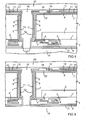
- Figure 1 is a cross section of a semiconductor device comprising a through-substrate via. It comprises a substrate 1 of semiconductor material, which may be silicon, for instance. Components of an integrated circuit 2, which is schematically indicated, can be CMOS components, for instance. An intermetal dielectric 3 is arranged on a surface 1' of the substrate 1. Structured metal layers 4 are embedded in the intermetal dielectric 3 and connected with vertical interconnections 5 to form a wiring of the integrated circuit 2.
- One of the metal layers 4' comprises a contact area 4*, which is provided for a through-substrate via, in particular a through-silicon via in the case of a silicon substrate.
- the semiconductor material on the inner wall of the via hole 7 can be covered with an insulating layer 8, which may comprise an oxide of the semiconductor material and/or a doped region of the semiconductor material.
- the insulating layer 8 can also be provided on the opposite surface 1" of the substrate 1, outside the via hole 7, as shown in Figure 1 by way of example.
- a handling wafer 14 is fastened to the device and can be bonded to the intermetal dielectric 3.
- a passivation layer 6 can be arranged on the intermetal dielectric 3 on the side facing away from the surface 1' of the substrate 1.
- a bonding layer 13, which may be an adhesive layer or may comprise an oxide of the semiconductor material, for instance, can be arranged between the passivation layer 6 and the handling wafer 14.
- Figure 2 is a cross section according to Figure 1 after an etching step, whereby a portion of the dielectric layer 3 is removed at the bottom of the via hole 7. Thus the contact area 4* is uncovered.
- the depth of the etching is controlled by the etch rate and the duration of the etching step.
- Figure 3 is a cross section according to Figure 2 after the formation of an electrically conductive interconnection through the via hole 7.
- a metallization 9 is applied in the via hole 7 on the insulating layer 8, the metallization 9 contacting the contact area 4*.
- a top metal 10 is arranged above the opposite surface 1" of the substrate 1 and can especially be insulated from the semiconductor material by the insulating layer 8.
- the top metal 10 can be part of the metallization 9 or a separate layer electrically connected to the metallization 9 and can comprise two or more partial layers including a barrier layer, for instance.
- the top metal 10 can be structured as indicated in Figure 3 .
- the intermetal dielectric 3 can be much thinner than the substrate 1. Consequently, the layers at the bottom of the through-substrate via can form a relatively thin membrane, which is liable to being damaged, thus adversely affecting the manufacturing process or the function of the device.
- the further process steps aim at avoiding the presence of the membrane.
- Figure 4 is a cross section according to Figure 3 after the application of a passivation layer 11 on the top metal 10 and a mask 15 above the opposite surface 1" of the substrate 1.
- the passivation layer 11 can be arranged on the sidewall within the via hole 7, and it can also be arranged above the opposite surface 1", so that it may completely cover the top metal 10 and can provide a conformal coating.
- the passivation layer 11 comprises a dielectric material, such as silicon dioxide, which can be applied by deposition.
- the mask 15 may be a resist mask, for instance, and is used in an anisotropic etching step, whereby the metallization 9 is removed from an area of the intermetal dielectric 3.
- the lateral boundaries of the region 16* of material that is to be removed are indicated in Figure 4 by vertical broken lines.
- Figure 5 is a cross section according to Figure 4 after the formation of a hole 16 in the region 16* indicated in Figure 4 by vertical broken lines.
- the mask 15 has been removed.
- the hole 16 extends the via hole 7 through the wiring.
- the passivation layer 6 and the bonding layer 13 may also be removed at the bottom 16' of the hole 16, but especially the bonding layer 13, which can serve as an etch stop layer, may still be present, at least partially, at the bottom 16' of the hole 16. This option is indicated in Figure 5 by a horizontal broken line.
- a further passivation layer 12 which may comprise Si 3 N 4 , for instance, can then be applied on the passivation layer 11, especially on the surface within the via hole 7, and on the surface within the hole 16 including the bottom 16', where a bottom portion 12', 12" of the further passivation layer 12 is arranged.
- the further passivation layer 12 may also be applied above the top metal 10.
- Figure 5 shows the case in which the bonding layer 13 has been removed from the bottom 16' of the hole 16, and the bottom portion 12' of the further passivation layer 12 is applied on a surface area of the handling wafer 14. If the passivation layer 6 has not been removed from the bottom 16' of the hole 16, the further passivation layer 12 comprises an alternative bottom portion 12", which is located on the passivation layer 6.
- the alternative bottom portion 12" is indicated in Figure 5 by a dotted line.
- Figure 6 is a cross section according to Figure 5 after the application of a further mask 17, which may also be a resist mask, for instance.
- the further mask 17 is used to remove the passivation layer 11 and the further passivation layer 12 above a contact area 10' of the top metal 10.
- the further passivation layer 12 may optionally be removed in an area of the bottom 16' of the hole 16 by an anisotropic etching step.
- the optional mask region 17' indicated in Figure 5 by a dotted area is absent, and the further mask 17 may include an alternative mask region 17" framing the opening of the mask, as shown in Figure 5 by vertical broken lines.
- the bonding layer 13 is still present at the bottom 16' of the hole 16, the further mask 17 can also be used to remove the bonding layer 13, from the bottom 16' of the hole 16.
- the handling wafer 14 may be used as an etch stop in this case.
- Figure 7 is a cross section according to Figure 6 after the passivation layers 11, 12 are structured and a further handling wafer 20 is attached.
- the bonding and filler material 19 may fill the hole 16 and the inner void of the via hole 7, which is not filled with the metallization 9.
- the further handling wafer 20 can be fastened to the bonding and filler material 19.
- Figure 7 shows the case in which the bottom portion 12' of the further passivation layer 12 is applied directly on the handling wafer 14 and is still present when the further handling wafer 20 is attached.
- This illustration corresponds to the first alternative case including the optional mask region 17' and the bottom portion 12' as shown in Figure 6 .
- Figure 8 is a cross section according to Figure 7 for the second alternative case, in which the further passivation layer 12 is removed from the bottom 16' of the hole 16 by an essentially anisotropic etching step using the further mask 17 having an opening instead of the optional mask region 17', and Figure 8 shows the intermediate product thus obtained after the removal of the further mask 17.
- the further passivation layer 12 still covers the sidewall of the hole 16 as a layer of essentially constant thickness. Small protrusions 12''' of the further passivation layer 12 may remain at the bottom 16' of the hole 16. These protrusions 12''' may be removed in a later process step.
- the passivation layer 6 and the further passivation layer 12 adjoin one another, so that the passivation layers 6, 12 form a continuous passivating layer and the passivation is not interrupted at the edges of the hole 16.
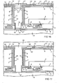
- Figure 9 is a cross section according to Figure 7 after the removal of the handling wafer 14 and the bottom portion 12' of the further passivation layer 12. If the further passivation layer 12 comprises the alternative bottom portion 12", sections of the bonding layer 13 and optionally the passivation layer 6 are still present between the bonding and filler material 19 and the alternative bottom portion 12'', and these sections are also removed until the bonding and filler material 19 is exposed. Figure 9 shows how the bottom surface of the bonding and filler material 19 is laid bare after this process step.
- Figure 10 is a cross section according to Figure 9 after an application of an optional component 21, which may be an optical filter, for instance.
- the optional component 21 can be formed on the surface of the passivation layer 6 and above optically sensitive elements of the integrated circuit 2, for instance.
- Figure 11 is a cross section according to Figure 10 after the removal of the further handling wafer 20 and the bonding and filler material 19.
- a tape 23, in particular an adhesive tape 23 can be applied to the device above the surface 1'.
- the further passivation layer 12 abuts the passivation layer 6.
- a solder ball 22 can be applied to the contact area 10' of the top metal 10, as shown in Figure 11 .
- the solder ball 22 can serve as an outer electric terminal of the electric interconnection through the substrate 1, which is formed by the metallization 9.
- An inner diameter D of the metallization 9 is typically larger than the diameter d of the hole 16, because the metallization 9 extends onto the contact area 4* surrounding the hole 16. Further process steps may follow before and after the tape 23 is removed.
- Figure 12 is a cross section according to Figure 2 for an alternative structure.
- the elements corresponding to elements shown in Figure 2 are designated in Figure 12 with the same reference numerals.
- the metal layer 4' comprising the contact area 4* is present in the entire area of the bottom of the via hole 7.
- this metal layer 4' can be employed as an etching stop layer in the etching step that is applied to remove the upper portion of the intermetal dielectric 3 beneath the via hole 7.
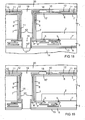
- Figure 13 is a cross section according to Figure 12 after the application of the metallization 9 in the via hole 7 and on the contact area 4*, as well as a top metal 10 outside the via hole 7.
- Figure 14 is a cross section according to Figure 13 after the application of the passivation layer 11 on the top metal 10 and the subsequent application of the mask 15 as described above.
- the hole 16 is formed in the region 16* indicated in Figure 14 by vertical broken lines. A portion of the metal layer 4' comprising the contact area 4* and a region of the intermetal dielectric 3 below are removed.
- Figure 15 is a cross section according to Figure 14 after the formation of the hole 16 extending the via hole 7.
- the mask 15 has been removed.
- the bottom portion 12', 12" of the further passivation layer 12 can be applied as described above in conjunction with Figure 5 .
- Figure 16 is a cross section according to Figure 15 after the application of the further passivation layer 12 and the further mask 17.
- the further mask 17 may comprise an optional mask region 17' or an alternative mask region 17" as described above.
- Figure 17 is a cross section according to Figure 16 after the passivation layers 11, 12 are structured, and the bonding and filler material 19 and the further handling wafer 20 are applied.
- Figure 17 shows the case in which the bonding layer 13 has been removed from the bottom 16' of the hole 16, and the bottom portion 12' of the further passivation layer 12 is applied on a surface area of the handling wafer 14.
- Figure 18 is a cross section according to Figure 16 , and an alternative to Figure 17 , after the passivation layers 11, 12 are structured and removed from the bottom of the hole 16, and the bonding and filler material 19 and the further handling wafer 20 are applied.
- the further passivation layer 12 is removed from the bottom 16' of the hole 16 by an essentially anisotropic etching step using the further mask 17.
- the further passivation layer 12 still covers the sidewall of the hole 16, and the small protrusions 12''' may remain at the bottom 16' of the hole 16 or later be removed.
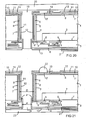
- Figure 19 is a cross section according to Figure 17 after the removal of the handling wafer and the removal of the further passivation layer 12 from the bottom of the hole 16. If the further passivation layer 12 comprises the alternative bottom portion 12", sections of the bonding layer 13 and optionally the passivation layer 6 are still present between the bonding and filler material 19 and the alternative bottom portion 12", and these sections are also removed until the bonding and filler material 19 is exposed. Figure 19 shows how the bottom surface of the bonding and filler material 19 is laid bare after this process step.
- Figure 20 is a cross section according to Figure 19 after an application of an optional component.
- Figure 21 is a cross section according to Figure 20 after the removal of the further handling wafer and an application of solder balls, similar to the device shown in Figure 11 .
- Figure 22 is a cross section according to Figure 5 for an alternative method.
- the elements corresponding to elements shown in Figure 5 are designated in Figure 22 with the same reference numerals.
- Figure 22 shows the via hole 7, the insulating layer 8, the metallization 9 in the via hole 7, the top metal 10, the passivation layer 11, the further passivation layer 12, the bonding layer 13 and the handling wafer 14.
- the metallization 9, the passivation layer 11 and the further passivation layer 12 are arranged on the sidewall and on the intermetal dielectric 3 at the bottom of the via hole 7.
- the metallization 9 contacts the contact area 4* of one of the metal layers 4' of the wiring.
- Figure 23 is a cross section according to Figure 22 after the application of the mask for structuring the passivation layers.
- This mask will be referred to as the further mask 17, since its purpose is similar to the purpose of the further mask 17 shown in Figure 6 .
- the further mask 17 is used to remove the passivation layer 11 and the further passivation layer 12 above a contact area 10' of the top metal 10.
- Figure 24 is a cross section according to Figure 23 after the passivation layers 11, 12 are structured and a further handling wafer 20 is applied.
- the further handling wafer 20 is fastened to the top surface of the device above the opposite surface 1" by means of a bonding and filler material 19, which may comprise an adhesive or an oxide of the semiconductor material, for instance. It may suffice to apply the bonding and filler material 19 only on the top surface outside the via hole 7, but the inner void of the via hole 7, which is not filled with the metallization 9, may be filled with the bonding and filler material 19 as well.
- Figure 25 is a cross section according to Figure 24 after the handling wafer 14 is replaced with a mask for forming a hole extending the via hole 7.
- This mask will be referred to as the mask 15, since its purpose is similar to the purpose of the mask 15 shown in Figure 4 .
- the mask 15 may be a resist mask, for instance, and is arranged above the surface 1'.
- the mask 15 can be applied on the intermetal dielectric 3 or on the passivation layer 6 that is arranged on the intermetal dielectric 3.
- the mask 15 is used in an anisotropic etching step, whereby a hole is formed in the region 16* that is present between the boundaries indicated in Figure 25 by vertical broken lines.
- Figure 26 is a cross section according to Figure 25 after the etching step forming the hole 16 and after the removal of the mask 15.
- a further passivation layer 24, which may comprise Si 3 N 4 , for instance, is applied on the inner surfaces of the hole 16.
- a continuous passivating layer is formed including the passivation layers 6, 11 and the further passivation layers 12, 24, and the passivation is not interrupted at the edges of the hole 16.
- Figure 27 is a cross section according to Figure 26 after the application of a further mask 25 for structuring the further passivation layer 24 in the hole 16.
- the further mask 25 can be a further resist mask, for instance. It may be advantageous if the further mask 25 not only covers the point where the passivation layer 6 adjoins the further passivation layer 24, but slightly overhangs the portion of the further passivation layer 24 that is present on the sidewall of the hole 16.
- Figure 28 is a cross section according to Figure 27 after the bottom of the further passivation layer 24 is removed by an anisotropic etching step through the opening of the further mask 25. If the further mask 25 slightly overhangs the portion of the further passivation layer 24 that is present on the sidewall of the hole 16, the anisotropic etching step leaves small pedestals 26 at the bottom of the hole 16. This shape of the remaining further passivation layer 24 secures that the further passivation layers 12 and 24 adjoin each other and a continous passivation is obtained. The further mask 25 is then removed, and an optional component 21 can be mounted to the device as described above.
- Figure 29 is a cross section according to Figure 28 after the removal of the further handling wafer 20 and the bonding and filler material 19 and an application of a solder ball 22 on the contact area 10'.
- arrows indicate the points where the passivation layers 6, 11, 12, 24 abut in order to achieve a continuous passivation of the surfaces inside and outside the via hole 7.
- the uninterrupted passivation is a further major advantage of the described semiconductor devices and manufacturing methods.
- Figure 30 is a cross section according to Figure 1 , including an indication of a region 16* of the intermetal dielectric 3 to be removed in order to obtain an alternative device structure.
- Figure 31 is a cross section according to Figure 30 after the formation of the hole 16, which extends to the passivation layer 6.
- the metallization 9 contacts the metal layer 4' laterally, so that the metallization 9 forms a smooth layer on the sidewall.
- Figure 32 is a cross section according to Figure 31 after an application of solder balls and an optical component.
- the device thus obtained corresponds to the devices shown in Figures 11 and 29 , but differs in the feature that the diameter of the hole d and the outer diameter of the metallization D' are equal.
- the described through-substrate vias have the advantage that they are capable of simultaneously transmitting optical and electrical signals.
- the described structure enhances the optical transmission, since a material interface causing absorption or diffraction is avoided.
- the described method can favourably be used to produce wafer-level chip-scale packages with mechanically stable through-substrate vias.
Landscapes
- Internal Circuitry In Semiconductor Integrated Circuit Devices (AREA)
Abstract
An intermetal dielectric (3) and metal layers (4) embedded in the intermetal dielectric (3) are arranged on a substrate (1) of semiconductor material. A via hole (7) is formed in the substrate, and a metallization (9) contacting a contact area (4*) of one of the metal layers (4') is applied in the via hole. The metallization (9), the metal layer (4') comprising the contact area (4*) and the intermetal dielectric (3) are partially removed at the bottom of the via hole in order to form a hole (16) penetrating the intermetal dielectric and extending the via hole. A continuous passivation (12) is arranged on sidewalls within the via hole (7) and the hole (16), and the metallization (9) contacts the contact area (4*) around the hole (16). Thus the presence of a thin membrane of layers, which is usually formed at the bottom of a hollow through-substrate via, is avoided.
Description
- The present invention relates to semiconductor devices comprising a through-substrate via.
- Three-dimensional integration of semiconductor devices uses through-silicon vias or through-substrate vias (TSVs) for electric interconnections. An electrically conductive layer, which may be a metallization, is typically arranged on the wall of the via hole to form the electric interconnection, and a void is left inside the via. Thus a thin structure resembling a membrane is created at the bottom of the TSV and may include a plurality of sublayers comprising metals and dielectrics with a total thickness of typically up to 10 µm. When the semiconductor device comprising the TSV is handled during the manufacturing process, thermomechanical stress may occur in the semiconductor substrate, and the bottom structure of the TSV may be bent or even broken.
- A mechanical stabilization of the bottom structure of the TSV can be achieved in different ways, such as an application of protective coatings or layers, and a reduction of the diameter of the bottom structure. A problem arising from the application of a plurality of layers is the mismatch of the coefficients of thermal expansion (CTE) of these layers. Experimental observations supported by simulations have demonstrated that cracks in the membrane are more probable if the number of layers constituting the membrane is increased. It is an object of the present invention to provide a mechanical stabilization for through-substrate vias of semiconductor devices.
- This object is achieved with the semiconductor device according to
claim 1 and the method of producing a semiconductor device according toclaim 10. Embodiments and variants derive from the dependent claims. - The semiconductor device comprises a substrate of semiconductor material, an intermetal dielectric on the substrate, metal layers embedded in the intermetal dielectric, a contact area of one of the metal layers, a via hole in the substrate opposite the contact area, and a metallization arranged in the via hole, the metallization contacting the contact area. A hole is arranged in the intermetal dielectric and forms an extension of the via hole. The intermetal dielectric and the metal layer comprising the contact area are penetrated by the hole. A continuous passivation is arranged on sidewalls within the via hole and the hole. The metallization contacts the contact area around the hole.
- An embodiment of the semiconductor device comprises a passivation layer, the intermetal dielectric being arranged between the substrate and the passivation layer. The passivation layer abuts the continuous passivation arranged on the sidewall within the hole. The passivation layer and the continuous passivation arranged on sidewalls within the via hole and the hole adjoin one another. An advantage of this arrangement is that the passivation is not interrupted at the edges of the hole.
- In a further embodiment of the semiconductor device, the via hole is clad with an insulating layer on a sidewall of the via hole, and the metallization forms a layer on the insulating layer. An advantage is that the metallization is thus insulated from the substrate to avoid short circuits, and a further advantage is that the insulation can be provided by a standard process step.
- In a further embodiment of the semiconductor device, the metallization comprises an inner diameter inside the via hole, the hole comprises an inner diameter parallel to the inner diameter of the metallization, and the inner diameter of the metallization is larger than the inner diameter of the hole. An advantage of this structure is that it facilitates the application of the metallization, and a further advantage is that it can be produced by etching the hole from the side opposite the intermetal dielectric.
- In a further embodiment of the semiconductor device, the metallization comprises an outer diameter inside the via hole, the hole comprises an inner diameter parallel to the outer diameter of the metallization, and the outer diameter of the metallization equals the inner diameter of the hole. An advantage of this structure is that a step or discontinuity inside the metallization is thus avoided.
- In a further embodiment of the semiconductor device, the continuous passivation is formed by a continuous passivation layer. An advantage of the continuous passivation layer is that it secures a continuous passivation, and a further advantage is that it can be applied in a single process step. A further embodiment of the semiconductor device comprises a passivation layer of the continuous passivation in the via hole and a further passivation layer of the continuous passivation in the hole, and the passivation layer abuts the further passivation layer. An advantage of this arrangement is that the passivation layers can be applied from opposite sides, and a smaller depth of the layers is required.
- In a further embodiment of the semiconductor device, a pedestal is formed by the further passivation layer where the further passivation layer abuts the passivation layer. This shape of the further passivation layer secures that the passivation layers adjoin each other and a continous passivation is thus obtained.
- The semiconductor device can be implemented in a variety of applications. It is especially useful in photonic devices, in particular high-frequency photonic devices. The application of the semiconductor device in photonic devices has the advantage that the open via can be used for an optical transmission that does not suffer from absorption or diffraction.
- Such applications include 3D cameras, in particular structured light cameras, time-of-flight cameras and stereoscopic imaging devices, CMOS imaging sensors, in particular rolling shutter image sensors, line scan image sensors and camera modules, lidar detectors using vertical-cavity surface-emitting lasers, various light sensors, in particular ambient light sensors, colour sensors, proximity sensors, gesture sensors, devices for optical character recognition or edge detection, in particular in products such as copiers, document scanners, spectral sensing devices or spectrum analyzers.
- In the method of producing a semiconductor device, an intermetal dielectric and metal layers embedded in the intermetal dielectric are arranged on a surface of a substrate of semiconductor material, a via hole is formed in the substrate, a metallization is applied in the via hole, the metallization contacting a contact area of one of the metal layers, and a mask comprising an opening above the via hole is applied. A hole is formed by partially removing the metallization, the metal layer comprising the contact area and the intermetal dieletric through the opening of the mask, so that the hole penetrates the intermetal dielectric and extends the via hole. A continuous passivation is formed on sidewalls within the via hole and the hole.
- In a variant of the method, a passivation layer is arranged on the intermetal dielectric opposite the surface of the substrate, and the continuous passivation is formed abutting the passivation layer. The passivation layer and the continuous passivation arranged on sidewalls within the via hole and the hole adjoin one another. An advantage of this arrangement is that the passivation is not interrupted at the edges of the hole, and a further advantage is that the passivation is easily produced in this way.
- In a further variant of the method, the mask is applied above the surface of the substrate. Applying the mask above the surface allows to produce the hole from the side where the intermetal dielectric is present, which requires a smaller etching depth. In particular, before the hole is formed, a further passivation layer is applied on the sidewall within the via hole, and after the hole is formed, a further passivation layer is applied on the sidewall within the hole, the further passivation layers forming the continuous passivation. This arrangement has the advantage that the passivation on the sidewall within the hole adjoins both the passivation on the sidewall of the via hole and the further passivation layer, and the connection of the passivation layers at the edges of the hole is more precisely produced in this way.
- In a further variant of the method, the mask is applied above an opposite surface of the substrate. Applying the mask above the opposite surface allows to produce the hole directly through the via hole in essentially the same method step, thus facilitating the process. In particular, after the hole is formed, a further passivation layer is applied on the sidewalls within the via hole and the hole to form the continuous passivation. Producing the hole directly through the via hole and forming the continuous passivation in one step both in the via hole and in the hole facilitates the process of forming a continuous passivation and improves the passivation.
- Before the hole is formed, a handling wafer can be attached to the intermetal dielectric. Then the further passivation layer is applied, a bottom portion of the further passivation layer covering an area of the handling wafer at the bottom of the hole, and the bottom portion is removed using a further mask, which is applied above the opposite surface of the substrate. Alternatively, the bottom portion is removed from the side above the surface of the substrate.
- A top metal can be formed above an opposite surface of the substrate, the top metal being electrically connected to the metallization, a passivation layer is applied on the metallization and the top metal, a further mask with an opening above a contact area of the top metal is applied, and the passivation layer is removed from the contact area through the opening of the further mask.
- After the passivation layer is applied and the hole is formed, a further passivation layer can be applied on the sidewalls within the via hole and the hole to form the continuous passivation, the further passivation layer comprising a bottom portion at a bottom of the hole, the further mask is applied after the formation of the further passivation layer, and the further mask is also used to remove the bottom portion of the further passivation layer.
- The following is a detailed description of examples of the semiconductor device and examples of the method of production in conjunction with the appended figures, which are not drawn to scale.
- Figure 1
- is a cross section of an intermediate product of a semiconductor device comprising a via hole and including a handling wafer.
- Figure 2
- is a cross section according to
Figure 1 after a partial removal of a dielectric layer. - Figure 3
- is a cross section according to
Figure 2 after the application of a metallization in the via hole and a top metal outside the via hole - Figure 4
- is a cross section according to
Figure 3 after the application of a passivation layer on the top metal and the subsequent application of a mask. - Figure 5
- is a cross section according to
Figure 4 after the formation of a hole extending the via hole, the removal of the mask and the application of a further passivation layer. - Figure 6
- is a cross section according to
Figure 5 after the application of a further passivation layer and a further mask. - Figure 7
- is a cross section according to
Figure 6 after the passivation layers are structured and a further handling wafer is applied. - Figure 8
- is a cross section according to
Figure 6 , and an alternative toFigure 7 , after the passivation layers are structured and removed from the bottom of the hole and a further handling wafer is applied. - Figure 9
- is a cross section according to
Figure 7 after the removal of the handling wafer and the removal of the further passivation layer from the bottom of the hole. - Figure 10
- is a cross section according to
Figure 9 after an application of an optional component. - Figure 11
- is a cross section according to
Figure 10 after the removal of the further handling wafer and an application of solder balls. - Figure 12
- is a cross section of an intermediate product of a semiconductor device comprising a via hole and including a handling wafer as an alternative to
Figure 2 . - Figure 13
- is a cross section according to
Figure 12 after the application of a metallization in the via hole and a top metal outside the via hole. - Figure 14
- is a cross section according to
Figure 13 after the application of a passivation layer on the top metal and the subsequent application of a mask. - Figure 15
- is a cross section according to
Figure 14 after the formation of a hole extending the via hole, the removal of the mask and the application of a further passivation layer. - Figure 16
- is a cross section according to
Figure 15 after the application of a further passivation layer and a further mask. - Figure 17
- is a cross section according to
Figure 16 after the passivation layers are structured and a further handling wafer is applied. - Figure 18
- is a cross section according to
Figure 16 , and an alternative toFigure 17 , after the passivation layers are structured and removed from the bottom of the hole and a further handling wafer is applied. - Figure 19
- is a cross section according to
Figure 17 after the removal of the handling wafer and the removal of the further passivation layer from the bottom of the hole. - Figure 20
- is a cross section according to
Figure 19 after an application of an optional component. - Figure 21
- is a cross section according to
Figure 20 after the removal of the further handling wafer and an application of solder balls. - Figure 22
- is a cross section according to
Figure 4 after the application of a metallization in the via hole, a top metal and passivation layers. - Figure 23
- is a cross section according to
Figure 22 after the application of the mask for structuring the passivation layers. - Figure 24
- is a cross section according to
Figure 23 after the passivation layers are structured and a further handling wafer is applied. - Figure 25
- is a cross section according to
Figure 24 after the handling wafer is replaced with a mask for forming a hole extending the via hole. - Figure 26
- is a cross section according to
Figure 25 after the formation of the hole extending the via hole, the removal of the mask and the application of a further passivation layer. - Figure 27
- is a cross section according to
Figure 26 after the application of a further mask for structuring the further passivation layer. - Figure 28
- is a cross section according to
Figure 27 after the bottom of the further passivation layer is removed. - Figure 29
- is a cross section according to
Figure 28 after the removal of the further handling wafer and an application of solder balls and an optical component. - Figure 30
- is a cross section according to
Figure 1 , including an indication of a region of material to be removed. - Figure 31
- is a cross section according to
Figure 30 after the application of a metallization in the via hole and the hole extending the via hole. - Figure 32
- is a cross section according to
Figure 31 after an application of solder balls and an optical component. -
Figure 1 is a cross section of a semiconductor device comprising a through-substrate via. It comprises asubstrate 1 of semiconductor material, which may be silicon, for instance. Components of anintegrated circuit 2, which is schematically indicated, can be CMOS components, for instance. Anintermetal dielectric 3 is arranged on a surface 1' of thesubstrate 1.Structured metal layers 4 are embedded in theintermetal dielectric 3 and connected withvertical interconnections 5 to form a wiring of theintegrated circuit 2. - One of the metal layers 4' comprises a
contact area 4*, which is provided for a through-substrate via, in particular a through-silicon via in the case of a silicon substrate. The semiconductor material on the inner wall of the viahole 7 can be covered with an insulatinglayer 8, which may comprise an oxide of the semiconductor material and/or a doped region of the semiconductor material. The insulatinglayer 8 can also be provided on theopposite surface 1" of thesubstrate 1, outside the viahole 7, as shown inFigure 1 by way of example. - A handling
wafer 14 is fastened to the device and can be bonded to theintermetal dielectric 3. In the example shown inFigure 1 , apassivation layer 6 can be arranged on theintermetal dielectric 3 on the side facing away from the surface 1' of thesubstrate 1. Abonding layer 13, which may be an adhesive layer or may comprise an oxide of the semiconductor material, for instance, can be arranged between thepassivation layer 6 and the handlingwafer 14. -
Figure 2 is a cross section according toFigure 1 after an etching step, whereby a portion of thedielectric layer 3 is removed at the bottom of the viahole 7. Thus thecontact area 4* is uncovered. The depth of the etching is controlled by the etch rate and the duration of the etching step. -
Figure 3 is a cross section according toFigure 2 after the formation of an electrically conductive interconnection through the viahole 7. Ametallization 9 is applied in the viahole 7 on the insulatinglayer 8, themetallization 9 contacting thecontact area 4*. Atop metal 10 is arranged above theopposite surface 1" of thesubstrate 1 and can especially be insulated from the semiconductor material by the insulatinglayer 8. Thetop metal 10 can be part of themetallization 9 or a separate layer electrically connected to themetallization 9 and can comprise two or more partial layers including a barrier layer, for instance. Thetop metal 10 can be structured as indicated inFigure 3 . - The
intermetal dielectric 3 can be much thinner than thesubstrate 1. Consequently, the layers at the bottom of the through-substrate via can form a relatively thin membrane, which is liable to being damaged, thus adversely affecting the manufacturing process or the function of the device. The further process steps aim at avoiding the presence of the membrane. -
Figure 4 is a cross section according toFigure 3 after the application of apassivation layer 11 on thetop metal 10 and amask 15 above theopposite surface 1" of thesubstrate 1. Thepassivation layer 11 can be arranged on the sidewall within the viahole 7, and it can also be arranged above theopposite surface 1", so that it may completely cover thetop metal 10 and can provide a conformal coating. Thepassivation layer 11 comprises a dielectric material, such as silicon dioxide, which can be applied by deposition. - The
mask 15 may be a resist mask, for instance, and is used in an anisotropic etching step, whereby themetallization 9 is removed from an area of theintermetal dielectric 3. The lateral boundaries of theregion 16* of material that is to be removed are indicated inFigure 4 by vertical broken lines. -
Figure 5 is a cross section according toFigure 4 after the formation of ahole 16 in theregion 16* indicated inFigure 4 by vertical broken lines. Themask 15 has been removed. Thehole 16 extends the viahole 7 through the wiring. Thus the thin membrane of layers at the bottom of the through-substrate via is removed, and the risk of a damage caused by cracks in the membrane is avoided. Thepassivation layer 6 and thebonding layer 13 may also be removed at the bottom 16' of thehole 16, but especially thebonding layer 13, which can serve as an etch stop layer, may still be present, at least partially, at the bottom 16' of thehole 16. This option is indicated inFigure 5 by a horizontal broken line. - A
further passivation layer 12, which may comprise Si3N4, for instance, can then be applied on thepassivation layer 11, especially on the surface within the viahole 7, and on the surface within thehole 16 including the bottom 16', where abottom portion 12', 12" of thefurther passivation layer 12 is arranged. Thefurther passivation layer 12 may also be applied above thetop metal 10. -
Figure 5 shows the case in which thebonding layer 13 has been removed from the bottom 16' of thehole 16, and the bottom portion 12' of thefurther passivation layer 12 is applied on a surface area of the handlingwafer 14. If thepassivation layer 6 has not been removed from the bottom 16' of thehole 16, thefurther passivation layer 12 comprises analternative bottom portion 12", which is located on thepassivation layer 6. Thealternative bottom portion 12" is indicated inFigure 5 by a dotted line. -
Figure 6 is a cross section according toFigure 5 after the application of afurther mask 17, which may also be a resist mask, for instance. Thefurther mask 17 is used to remove thepassivation layer 11 and thefurther passivation layer 12 above a contact area 10' of thetop metal 10. Thefurther passivation layer 12 may optionally be removed in an area of the bottom 16' of thehole 16 by an anisotropic etching step. In this case the optional mask region 17' indicated inFigure 5 by a dotted area is absent, and thefurther mask 17 may include analternative mask region 17" framing the opening of the mask, as shown inFigure 5 by vertical broken lines. If thebonding layer 13 is still present at the bottom 16' of thehole 16, thefurther mask 17 can also be used to remove thebonding layer 13, from the bottom 16' of thehole 16. The handlingwafer 14 may be used as an etch stop in this case. -
Figure 7 is a cross section according toFigure 6 after the passivation layers 11, 12 are structured and afurther handling wafer 20 is attached. A bonding andfiller material 19, which may comprise an adhesive or an oxide of the semiconductor material, for instance, is applied in the viahole 7 and to the top surface including the remaining upper portions of thepassivation layer 11 and thefurther passivation layer 12. The bonding andfiller material 19 may fill thehole 16 and the inner void of the viahole 7, which is not filled with themetallization 9. Thefurther handling wafer 20 can be fastened to the bonding andfiller material 19. -
Figure 7 shows the case in which the bottom portion 12' of thefurther passivation layer 12 is applied directly on the handlingwafer 14 and is still present when thefurther handling wafer 20 is attached. This illustration corresponds to the first alternative case including the optional mask region 17' and the bottom portion 12' as shown inFigure 6 . -
Figure 8 is a cross section according toFigure 7 for the second alternative case, in which thefurther passivation layer 12 is removed from the bottom 16' of thehole 16 by an essentially anisotropic etching step using thefurther mask 17 having an opening instead of the optional mask region 17', andFigure 8 shows the intermediate product thus obtained after the removal of thefurther mask 17. Thefurther passivation layer 12 still covers the sidewall of thehole 16 as a layer of essentially constant thickness. Small protrusions 12''' of thefurther passivation layer 12 may remain at the bottom 16' of thehole 16. These protrusions 12''' may be removed in a later process step. In any case thepassivation layer 6 and thefurther passivation layer 12 adjoin one another, so that the passivation layers 6, 12 form a continuous passivating layer and the passivation is not interrupted at the edges of thehole 16. -
Figure 9 is a cross section according toFigure 7 after the removal of the handlingwafer 14 and the bottom portion 12' of thefurther passivation layer 12. If thefurther passivation layer 12 comprises thealternative bottom portion 12", sections of thebonding layer 13 and optionally thepassivation layer 6 are still present between the bonding andfiller material 19 and the alternative bottom portion 12'', and these sections are also removed until the bonding andfiller material 19 is exposed.Figure 9 shows how the bottom surface of the bonding andfiller material 19 is laid bare after this process step. -
Figure 10 is a cross section according toFigure 9 after an application of anoptional component 21, which may be an optical filter, for instance. Theoptional component 21 can be formed on the surface of thepassivation layer 6 and above optically sensitive elements of theintegrated circuit 2, for instance. -
Figure 11 is a cross section according toFigure 10 after the removal of thefurther handling wafer 20 and the bonding andfiller material 19. To aid these process steps, atape 23, in particular anadhesive tape 23, can be applied to the device above the surface 1'. Thefurther passivation layer 12 abuts thepassivation layer 6. Asolder ball 22 can be applied to the contact area 10' of thetop metal 10, as shown inFigure 11 . Thesolder ball 22 can serve as an outer electric terminal of the electric interconnection through thesubstrate 1, which is formed by themetallization 9. An inner diameter D of themetallization 9 is typically larger than the diameter d of thehole 16, because themetallization 9 extends onto thecontact area 4* surrounding thehole 16. Further process steps may follow before and after thetape 23 is removed. -
Figure 12 is a cross section according toFigure 2 for an alternative structure. The elements corresponding to elements shown inFigure 2 are designated inFigure 12 with the same reference numerals. In the alternative structure, the metal layer 4' comprising thecontact area 4* is present in the entire area of the bottom of the viahole 7. Hence this metal layer 4' can be employed as an etching stop layer in the etching step that is applied to remove the upper portion of theintermetal dielectric 3 beneath the viahole 7. -
Figure 13 is a cross section according toFigure 12 after the application of themetallization 9 in the viahole 7 and on thecontact area 4*, as well as atop metal 10 outside the viahole 7. -
Figure 14 is a cross section according toFigure 13 after the application of thepassivation layer 11 on thetop metal 10 and the subsequent application of themask 15 as described above. Thehole 16 is formed in theregion 16* indicated inFigure 14 by vertical broken lines. A portion of the metal layer 4' comprising thecontact area 4* and a region of theintermetal dielectric 3 below are removed. -
Figure 15 is a cross section according toFigure 14 after the formation of thehole 16 extending the viahole 7. Themask 15 has been removed. Thebottom portion 12', 12" of thefurther passivation layer 12 can be applied as described above in conjunction withFigure 5 . -
Figure 16 is a cross section according toFigure 15 after the application of thefurther passivation layer 12 and thefurther mask 17. Thefurther mask 17 may comprise an optional mask region 17' or analternative mask region 17" as described above. -
Figure 17 is a cross section according toFigure 16 after the passivation layers 11, 12 are structured, and the bonding andfiller material 19 and thefurther handling wafer 20 are applied.Figure 17 shows the case in which thebonding layer 13 has been removed from the bottom 16' of thehole 16, and the bottom portion 12' of thefurther passivation layer 12 is applied on a surface area of the handlingwafer 14. -
Figure 18 is a cross section according toFigure 16 , and an alternative toFigure 17 , after the passivation layers 11, 12 are structured and removed from the bottom of thehole 16, and the bonding andfiller material 19 and thefurther handling wafer 20 are applied. In the example ofFigure 18 , thefurther passivation layer 12 is removed from the bottom 16' of thehole 16 by an essentially anisotropic etching step using thefurther mask 17. Thefurther passivation layer 12 still covers the sidewall of thehole 16, and the small protrusions 12''' may remain at the bottom 16' of thehole 16 or later be removed. -
Figure 19 is a cross section according toFigure 17 after the removal of the handling wafer and the removal of thefurther passivation layer 12 from the bottom of thehole 16. If thefurther passivation layer 12 comprises thealternative bottom portion 12", sections of thebonding layer 13 and optionally thepassivation layer 6 are still present between the bonding andfiller material 19 and thealternative bottom portion 12", and these sections are also removed until the bonding andfiller material 19 is exposed.Figure 19 shows how the bottom surface of the bonding andfiller material 19 is laid bare after this process step. -
Figure 20 is a cross section according toFigure 19 after an application of an optional component. -
Figure 21 is a cross section according toFigure 20 after the removal of the further handling wafer and an application of solder balls, similar to the device shown inFigure 11 . -
Figure 22 is a cross section according toFigure 5 for an alternative method. The elements corresponding to elements shown inFigure 5 are designated inFigure 22 with the same reference numerals.Figure 22 shows the viahole 7, the insulatinglayer 8, themetallization 9 in the viahole 7, thetop metal 10, thepassivation layer 11, thefurther passivation layer 12, thebonding layer 13 and the handlingwafer 14. Themetallization 9, thepassivation layer 11 and thefurther passivation layer 12 are arranged on the sidewall and on theintermetal dielectric 3 at the bottom of the viahole 7. Themetallization 9 contacts thecontact area 4* of one of the metal layers 4' of the wiring. -
Figure 23 is a cross section according toFigure 22 after the application of the mask for structuring the passivation layers. This mask will be referred to as thefurther mask 17, since its purpose is similar to the purpose of thefurther mask 17 shown inFigure 6 . Thefurther mask 17 is used to remove thepassivation layer 11 and thefurther passivation layer 12 above a contact area 10' of thetop metal 10. -
Figure 24 is a cross section according toFigure 23 after the passivation layers 11, 12 are structured and afurther handling wafer 20 is applied. Thefurther handling wafer 20 is fastened to the top surface of the device above theopposite surface 1" by means of a bonding andfiller material 19, which may comprise an adhesive or an oxide of the semiconductor material, for instance. It may suffice to apply the bonding andfiller material 19 only on the top surface outside the viahole 7, but the inner void of the viahole 7, which is not filled with themetallization 9, may be filled with the bonding andfiller material 19 as well. -
Figure 25 is a cross section according toFigure 24 after the handlingwafer 14 is replaced with a mask for forming a hole extending the viahole 7. This mask will be referred to as themask 15, since its purpose is similar to the purpose of themask 15 shown inFigure 4 . Themask 15 may be a resist mask, for instance, and is arranged above the surface 1'. Themask 15 can be applied on theintermetal dielectric 3 or on thepassivation layer 6 that is arranged on theintermetal dielectric 3. Themask 15 is used in an anisotropic etching step, whereby a hole is formed in theregion 16* that is present between the boundaries indicated inFigure 25 by vertical broken lines. -
Figure 26 is a cross section according toFigure 25 after the etching step forming thehole 16 and after the removal of themask 15. Afurther passivation layer 24, which may comprise Si3N4, for instance, is applied on the inner surfaces of thehole 16. Thus a continuous passivating layer is formed including the passivation layers 6, 11 and the further passivation layers 12, 24, and the passivation is not interrupted at the edges of thehole 16. -
Figure 27 is a cross section according toFigure 26 after the application of afurther mask 25 for structuring thefurther passivation layer 24 in thehole 16. Thefurther mask 25 can be a further resist mask, for instance. It may be advantageous if thefurther mask 25 not only covers the point where thepassivation layer 6 adjoins thefurther passivation layer 24, but slightly overhangs the portion of thefurther passivation layer 24 that is present on the sidewall of thehole 16. -
Figure 28 is a cross section according toFigure 27 after the bottom of thefurther passivation layer 24 is removed by an anisotropic etching step through the opening of thefurther mask 25. If thefurther mask 25 slightly overhangs the portion of thefurther passivation layer 24 that is present on the sidewall of thehole 16, the anisotropic etching step leavessmall pedestals 26 at the bottom of thehole 16. This shape of the remainingfurther passivation layer 24 secures that the further passivation layers 12 and 24 adjoin each other and a continous passivation is obtained. Thefurther mask 25 is then removed, and anoptional component 21 can be mounted to the device as described above. -
Figure 29 is a cross section according toFigure 28 after the removal of thefurther handling wafer 20 and the bonding andfiller material 19 and an application of asolder ball 22 on the contact area 10'. Thus a device structure that is essentially similar to the device shown inFigure 11 is obtained. InFigure 29 , arrows indicate the points where the passivation layers 6, 11, 12, 24 abut in order to achieve a continuous passivation of the surfaces inside and outside the viahole 7. The uninterrupted passivation is a further major advantage of the described semiconductor devices and manufacturing methods. -
Figure 30 is a cross section according toFigure 1 , including an indication of aregion 16* of theintermetal dielectric 3 to be removed in order to obtain an alternative device structure. -
Figure 31 is a cross section according toFigure 30 after the formation of thehole 16, which extends to thepassivation layer 6. Themetallization 9 contacts the metal layer 4' laterally, so that themetallization 9 forms a smooth layer on the sidewall. -
Figure 32 is a cross section according toFigure 31 after an application of solder balls and an optical component. The device thus obtained corresponds to the devices shown inFigures 11 and29 , but differs in the feature that the diameter of the hole d and the outer diameter of the metallization D' are equal. - In the described device, the risks incurred by the presence of the layer membrane at the bottom of the through-substrate via are avoided. In some instances, the described through-substrate vias have the advantage that they are capable of simultaneously transmitting optical and electrical signals. In comparison with a closed structure comprising transparent layers, the described structure enhances the optical transmission, since a material interface causing absorption or diffraction is avoided. The described method can favourably be used to produce wafer-level chip-scale packages with mechanically stable through-substrate vias.
-
- 1
- substrate
- 1'
- surface
- 1"
- opposite surface
- 2
- integrated circuit
- 3
- intermetal dielectric
- 4
- metal layer
- 4'
- metal layer comprising a contact area
- 4*
- contact area
- 5
- vertical interconnection
- 6
- passivation layer
- 7
- via hole
- 8
- insulating layer
- 9
- metallization
- 10
- top metal
- 10'
- contact area of the top metal
- 11
- passivation layer
- 12
- further passivation layer
- 12'
- bottom portion
- 12"
- alternative bottom portion
- 12'''
- protrusion
- 13
- bonding layer
- 14
- handling wafer
- 15
- mask
- 16
- hole
- 16'
- bottom of the hole
- 16*
- region of material to be removed
- 17
- further mask
- 17'
- optional mask region
- 17"
- alternative mask region
- 18
- opening
- 19
- bonding and filler material
- 20
- further handling wafer
- 21
- optional component
- 22
- solder ball
- 23
- tape
- 24
- further passivation layer
- 25
- further mask
- 26
- pedestal
- d
- diameter of the hole
- D
- inner diameter of the metallization
- D'
- outer diameter of the metallization
Claims (15)
- A semiconductor device, comprising:a substrate (1) of semiconductor material,an intermetal dielectric (3) on the substrate (1),metal layers (4) embedded in the intermetal dielectric (3),a contact area (4*) of one of the metal layers (4'),a via hole (7) in the substrate (1) opposite the contact area (4*), anda metallization (9) arranged in the via hole (7), the metallization being in contact with the contact area (4*),characterized in thata hole (16) is arranged in the intermetal dielectric (3), the hole (16) forming an extension of the via hole (7),a continuous passivation (12, 24) is arranged on sidewalls within the via hole (7) and the hole (16), andthe metallization (9) is in contact with the contact area (4*) around the hole (16).
- The semiconductor device of claim 1, further comprising:a passivation layer (6), the intermetal dielectric (3) being arranged between the substrate (1) and the passivation layer (6), andthe passivation layer (6) abutting the continuous passivation (12, 24) arranged on the sidewall within the hole (16).
- The semiconductor device of claim 1 or 2, wherein an insulating layer (8) is arranged on a sidewall of the via hole (7), and the metallization (9) forms a layer on the insulating layer (8).
- The semiconductor device of one of claims 1 to 3, wherein the metallization (9) comprises an inner diameter (D) inside the via hole (7), the hole (16) comprises an inner diameter (d) parallel to the inner diameter (D) of the metallization (9), and the inner diameter (D) of the metallization (9) is larger than the inner diameter (d) of the hole (16).
- The semiconductor device of one of claims 1 to 4, wherein the metallization (9) comprises an outer diameter (D') inside the via hole (7), the hole (16) comprises an inner diameter (d) parallel to the outer diameter (D') of the metallization (9), and the outer diameter (D') of the metallization (9) equals the inner diameter (d) of the hole (16).
- The semiconductor device of one of claims 1 to 5, wherein the continuous passivation (12, 24) is formed by a continuous passivation layer (12).
- The semiconductor device of one of claims 1 to 5, further comprising:a passivation layer (12) of the continuous passivation (12, 24) in the via hole (7),a further passivation layer (24) of the continuous passivation (12, 24) in the hole (16), andthe passivation layer (12) of the continuous passivation (12, 24) abutting the further passivation layer (24) of the continuous passivation (12, 24).
- The semiconductor device of claim 7, further comprising:a pedestal (26) formed by the further passivation layer (24) where the further passivation layer (24) abuts the passivation layer (12).
- A device comprising a semiconductor device according to one of claims 1 to 8, the device being at least one of: a photonic device, high-frequency photonic device, 3D camera, structured light camera, time-of-flight camera, stereoscopic imaging device, CMOS imaging sensor, rolling shutter image sensor, line scan image sensor, camera module, lidar detector, ambient light sensor, colour sensor, proximity sensor, gesture sensor, device for optical character recognition or edge detection, photocopier, document scanner, spectral sensing device and spectrum analyzer.
- A method of producing a semiconductor device, comprising:arranging an intermetal dielectric (3) and metal layers (4) embedded in the intermetal dielectric (3) on a surface (1') of a substrate (1) of semiconductor material,forming a via hole (7) in the substrate (1),applying a metallization (9) in the via hole (7), the metallization (9) contacting a contact area (4*) of one of the metal layers (4'),applying a mask (15) comprising an opening above the via hole (7),forming a hole (16) by partially removing the metallization (9), the metal layer (4') comprising the contact area (4*) and the intermetal dieletric (3) through the opening of the mask (15), the hole (16) penetrating the intermetal dielectric (3) and extending the via hole (7), andforming a continuous passivation (12, 24) on sidewalls within the via hole (7) and the hole (16).
- The method of claim 10, further comprising:arranging a passivation layer (6) on the intermetal dielectric (3) opposite the surface (1') of the substrate (1), andforming the continuous passivation (12, 24) abutting the passivation layer (6).
- The method of claim 10 or 11, wherein
the mask (15) is applied above the surface (1') of the substrate (1), and
before the hole (16) is formed, a further passivation layer (12) is applied on the sidewall within the via hole (7), and after the hole (16) is formed, a further passivation layer (24) is applied on the sidewall within the hole (16), the further passivation layers (12, 24) forming the continuous passivation. - The method of claim 10 or 11, wherein
the mask (15) is applied above an opposite surface (1'') of the substrate (1), and
after the hole (16) is formed, a further passivation layer (12) is applied on the sidewalls within the via hole (7) and the hole (16) to form the continuous passivation. - The method of claim 13, wherein
before the hole (16) is formed, a handling wafer (14) is attached to the intermetal dielectric (3),
the further passivation layer (12) is applied, a bottom portion (12', 12*) of the further passivation layer (12) covering an area of the handling wafer (14) at the bottom (16*) of the hole (16), and
the bottom portion (12', 12*) is removed using a further mask (17), which is applied above the opposite surface (1'') of the substrate (1). - The method of claim 13, wherein
before the hole (16) is formed, a handling wafer (14) is attached to the intermetal dielectric (3),
the further passivation layer (12) is applied, a bottom portion (12', 12*) of the further passivation layer (12) covering an area of the handling wafer (14) at the bottom (16*) of the hole (16),
the handling wafer (14) is removed, and
the bottom portion (12', 12*) is removed from the side above the surface (1') of the substrate (1).
Priority Applications (6)
| Application Number | Priority Date | Filing Date | Title |
|---|---|---|---|
| EP18215468.2A EP3671823A1 (en) | 2018-12-21 | 2018-12-21 | Semiconductor device with through-substrate via and method of manufacturing a semiconductor device with through-substrate via |
| PCT/EP2019/086704 WO2020127988A1 (en) | 2018-12-21 | 2019-12-20 | Semiconductor device with through-substrate via and method of manufacturing a semiconductor device with through-substrate via |
| US17/415,167 US12100644B2 (en) | 2018-12-21 | 2019-12-20 | Semiconductor device with through-substrate via and method of manufacturing a semiconductor device with through-substrate via |
| EP19828762.5A EP3900030B1 (en) | 2018-12-21 | 2019-12-20 | Semiconductor device with through-substrate via and method of manufacturing a semiconductor device with through-substrate via |
| JP2021526542A JP7273153B2 (en) | 2018-12-21 | 2019-12-20 | Semiconductor device with through-substrate via and method for manufacturing semiconductor device with through-substrate via |
| CN201980078619.5A CN113474877B (en) | 2018-12-21 | 2019-12-20 | Semiconductor device having through substrate via and method of manufacturing semiconductor device having through substrate via |
Applications Claiming Priority (1)
| Application Number | Priority Date | Filing Date | Title |
|---|---|---|---|
| EP18215468.2A EP3671823A1 (en) | 2018-12-21 | 2018-12-21 | Semiconductor device with through-substrate via and method of manufacturing a semiconductor device with through-substrate via |
Publications (1)
| Publication Number | Publication Date |
|---|---|
| EP3671823A1 true EP3671823A1 (en) | 2020-06-24 |
Family
ID=64900816
Family Applications (2)
| Application Number | Title | Priority Date | Filing Date |
|---|---|---|---|
| EP18215468.2A Withdrawn EP3671823A1 (en) | 2018-12-21 | 2018-12-21 | Semiconductor device with through-substrate via and method of manufacturing a semiconductor device with through-substrate via |
| EP19828762.5A Active EP3900030B1 (en) | 2018-12-21 | 2019-12-20 | Semiconductor device with through-substrate via and method of manufacturing a semiconductor device with through-substrate via |
Family Applications After (1)
| Application Number | Title | Priority Date | Filing Date |
|---|---|---|---|
| EP19828762.5A Active EP3900030B1 (en) | 2018-12-21 | 2019-12-20 | Semiconductor device with through-substrate via and method of manufacturing a semiconductor device with through-substrate via |
Country Status (5)
| Country | Link |
|---|---|
| US (1) | US12100644B2 (en) |
| EP (2) | EP3671823A1 (en) |
| JP (1) | JP7273153B2 (en) |
| CN (1) | CN113474877B (en) |
| WO (1) | WO2020127988A1 (en) |
Citations (7)
| Publication number | Priority date | Publication date | Assignee | Title |
|---|---|---|---|---|
| US20080284041A1 (en) * | 2007-05-18 | 2008-11-20 | Samsung Electronics Co., Ltd. | Semiconductor package with through silicon via and related method of fabrication |
| WO2009013315A2 (en) * | 2007-07-24 | 2009-01-29 | Austriamicrosystems Ag | Semiconductor substrate with through-contact and method for production thereof |
| WO2009017835A2 (en) * | 2007-07-31 | 2009-02-05 | Tessera, Inc. | Semiconductor packaging process using through silicon vias |
| EP2597677A1 (en) * | 2011-11-23 | 2013-05-29 | austriamicrosystems AG | Semiconductor device with through-substrate via covered by a solder ball and related method of production |
| EP2741322A1 (en) * | 2012-12-10 | 2014-06-11 | ams AG | Semiconductor device with integrated hot plate and recessed substrate and method of production |
| JP2015228473A (en) * | 2014-06-03 | 2015-12-17 | パナソニックIpマネジメント株式会社 | Semiconductor device and manufacturing method thereof |
| WO2018123299A1 (en) * | 2016-12-26 | 2018-07-05 | ソニーセミコンダクタソリューションズ株式会社 | Semiconductor device, method for manufacturing semiconductor device, and solid-state image pickup element |
Family Cites Families (6)
| Publication number | Priority date | Publication date | Assignee | Title |
|---|---|---|---|---|
| DE10319538B4 (en) * | 2003-04-30 | 2008-01-17 | Qimonda Ag | Semiconductor device and method for producing a semiconductor device |
| DE102009004725A1 (en) | 2009-01-15 | 2010-07-29 | Austriamicrosystems Ag | Through-hole semiconductor circuit and method of manufacturing vertically integrated circuits |
| EP2306506B1 (en) | 2009-10-01 | 2013-07-31 | ams AG | Method of producing a semiconductor device having a through-wafer interconnect |
| EP2772939B1 (en) | 2013-03-01 | 2016-10-19 | Ams Ag | Semiconductor device for detection of radiation and method of producing a semiconductor device for detection of radiation |
| EP2860560B1 (en) | 2013-10-14 | 2019-07-24 | ams AG | Semiconductor device with optical and electrical vias |
| CN104752384B (en) | 2015-04-23 | 2018-06-22 | 华天科技(昆山)电子有限公司 | Semiconductor package and preparation method thereof |
-
2018
- 2018-12-21 EP EP18215468.2A patent/EP3671823A1/en not_active Withdrawn
-
2019
- 2019-12-20 JP JP2021526542A patent/JP7273153B2/en active Active
- 2019-12-20 US US17/415,167 patent/US12100644B2/en active Active
- 2019-12-20 EP EP19828762.5A patent/EP3900030B1/en active Active
- 2019-12-20 WO PCT/EP2019/086704 patent/WO2020127988A1/en not_active Ceased
- 2019-12-20 CN CN201980078619.5A patent/CN113474877B/en not_active Expired - Fee Related
Patent Citations (7)
| Publication number | Priority date | Publication date | Assignee | Title |
|---|---|---|---|---|
| US20080284041A1 (en) * | 2007-05-18 | 2008-11-20 | Samsung Electronics Co., Ltd. | Semiconductor package with through silicon via and related method of fabrication |
| WO2009013315A2 (en) * | 2007-07-24 | 2009-01-29 | Austriamicrosystems Ag | Semiconductor substrate with through-contact and method for production thereof |
| WO2009017835A2 (en) * | 2007-07-31 | 2009-02-05 | Tessera, Inc. | Semiconductor packaging process using through silicon vias |
| EP2597677A1 (en) * | 2011-11-23 | 2013-05-29 | austriamicrosystems AG | Semiconductor device with through-substrate via covered by a solder ball and related method of production |
| EP2741322A1 (en) * | 2012-12-10 | 2014-06-11 | ams AG | Semiconductor device with integrated hot plate and recessed substrate and method of production |
| JP2015228473A (en) * | 2014-06-03 | 2015-12-17 | パナソニックIpマネジメント株式会社 | Semiconductor device and manufacturing method thereof |
| WO2018123299A1 (en) * | 2016-12-26 | 2018-07-05 | ソニーセミコンダクタソリューションズ株式会社 | Semiconductor device, method for manufacturing semiconductor device, and solid-state image pickup element |
Also Published As
| Publication number | Publication date |
|---|---|
| JP7273153B2 (en) | 2023-05-12 |
| US20220059434A1 (en) | 2022-02-24 |
| WO2020127988A1 (en) | 2020-06-25 |
| CN113474877B (en) | 2024-08-02 |
| CN113474877A (en) | 2021-10-01 |
| EP3900030A1 (en) | 2021-10-27 |
| US12100644B2 (en) | 2024-09-24 |
| JP2022511415A (en) | 2022-01-31 |
| EP3900030B1 (en) | 2023-07-05 |
Similar Documents
| Publication | Publication Date | Title |
|---|---|---|
| CN101937894B (en) | Semiconductor device including through-electrode and method of manufacturing the same | |
| KR101626693B1 (en) | Semiconductor device and method for manufacturing same | |
| JP5618348B2 (en) | Semiconductor image sensor device and manufacturing method thereof | |
| KR101453158B1 (en) | Stepped package for image sensor and method of making same | |
| US8273657B2 (en) | Method for manufacturing a semiconductor apparatus having a through-hole interconnection | |
| US10109663B2 (en) | Chip package and method for forming the same | |
| US10153237B2 (en) | Chip package and method for forming the same | |
| US8623762B2 (en) | Semiconductor device and a method for making the semiconductor device | |
| CN114551338B (en) | Semiconductor device with buried metal pad and method of manufacturing the same | |
| US10032821B2 (en) | Imaging device and method of manufacturing the same | |
| US12100644B2 (en) | Semiconductor device with through-substrate via and method of manufacturing a semiconductor device with through-substrate via | |
| JP2010165804A (en) | Semiconductor device, electronic apparatus using the same, and method of manufacturing semiconductor device | |
| CN115377130A (en) | Image sensor, manufacturing method thereof and electronic device | |
| EP2889901B1 (en) | Semiconductor device with through-substrate via and corresponding method | |
| US20230352513A1 (en) | Electrical connection and its method of fabrication | |
| US20220102490A1 (en) | Method of manufacturing semiconductor structure | |
| WO2010131391A1 (en) | Semiconductor device and electronic device provided with same | |
| US20190206754A1 (en) | Electronic package and method of manufacturing the same | |
| US20260029576A1 (en) | Chip structure and semiconductor package including the same | |
| EP4425535A1 (en) | Semiconductor device, method for producing same, and electronic device | |
| EP3211672B1 (en) | Chip-scale package for an optical sensor semiconductor device with filter and method of producing a chip-scale package | |
| KR20240139552A (en) | Photoelectric conversion apparatus, photoelectric conversion system, and movable body | |
| CN117038679A (en) | A packaging structure, packaging method and terminal equipment | |
| KR100789625B1 (en) | CMOS image sensor and its manufacturing method | |
| CN118658865A (en) | Photoelectric conversion apparatus, photoelectric conversion system, and moving body |
Legal Events
| Date | Code | Title | Description |
|---|---|---|---|
| PUAI | Public reference made under article 153(3) epc to a published international application that has entered the european phase |
Free format text: ORIGINAL CODE: 0009012 |
|
| STAA | Information on the status of an ep patent application or granted ep patent |
Free format text: STATUS: THE APPLICATION HAS BEEN PUBLISHED |
|
| AK | Designated contracting states |
Kind code of ref document: A1 Designated state(s): AL AT BE BG CH CY CZ DE DK EE ES FI FR GB GR HR HU IE IS IT LI LT LU LV MC MK MT NL NO PL PT RO RS SE SI SK SM TR |
|
| AX | Request for extension of the european patent |
Extension state: BA ME |
|
| STAA | Information on the status of an ep patent application or granted ep patent |
Free format text: STATUS: THE APPLICATION IS DEEMED TO BE WITHDRAWN |
|
| 18D | Application deemed to be withdrawn |
Effective date: 20210112 |