EP3671298A1 - High-efficiency fiber-to-waveguide coupler - Google Patents
High-efficiency fiber-to-waveguide coupler Download PDFInfo
- Publication number
- EP3671298A1 EP3671298A1 EP19215444.1A EP19215444A EP3671298A1 EP 3671298 A1 EP3671298 A1 EP 3671298A1 EP 19215444 A EP19215444 A EP 19215444A EP 3671298 A1 EP3671298 A1 EP 3671298A1
- Authority
- EP
- European Patent Office
- Prior art keywords
- waveguide layer
- waveguides
- waveguide
- pair
- optical coupler
- Prior art date
- Legal status (The legal status is an assumption and is not a legal conclusion. Google has not performed a legal analysis and makes no representation as to the accuracy of the status listed.)
- Granted
Links
Images


Classifications
-
- G—PHYSICS
- G02—OPTICS
- G02B—OPTICAL ELEMENTS, SYSTEMS OR APPARATUS
- G02B6/00—Light guides; Structural details of arrangements comprising light guides and other optical elements, e.g. couplings
- G02B6/24—Coupling light guides
- G02B6/26—Optical coupling means
- G02B6/30—Optical coupling means for use between fibre and thin-film device
- G02B6/305—Optical coupling means for use between fibre and thin-film device and having an integrated mode-size expanding section, e.g. tapered waveguide
Definitions
- Integrated photonics offers significant advantages over fiber and free-space optics for a wide range of applications due to its ability to miniaturize optical fields while maintaining high degrees of robustness, resulting in reduced size, weight, and power consumption.
- one of the most significant limiting factors facing integrated photonics is the difficulty in interfacing with fiber optics. In coupling light from a fiber to a waveguide, several decibels of power are typically lost.
- lensed fibers or ultra-high numerical aperture fibers are butt-coupled to inverse tapers in integrated photonics chips.
- the minimum total facet loss that has been achieved in this way is about 0.4 dB, which corresponds to roughly 90% coupling efficiency.
- an even higher efficiency, ideally approaching 100%, is desired.
- An optical coupler comprises a waveguide structure including a first waveguide layer having a proximal end and a distal end, the first waveguide layer including a first pair of waveguides that extend from the proximal end along a first portion of the first waveguide layer, wherein the first pair of waveguides each widen along a second portion of the first waveguide layer such that the first pair of waveguides merge into a single waveguide toward the distal end.
- a second waveguide layer is separated from the first waveguide layer, with the second waveguide layer having a proximal end and a distal end, the second waveguide layer including a second pair of waveguides that extend from the proximal end of the second waveguide layer along a first portion of the second waveguide layer, wherein the second pair of waveguides each narrow along a second portion of the second waveguide layer to separate distal tips at the distal end of the second waveguide layer.
- the waveguide structure is configured to match an integrated photonics mode to a fiber mode supported by an optical fiber.
- the fiber-to-waveguide coupler includes a multi-layer waveguide structure that matches an integrated photonics mode to the mode supported by a standard optical fiber.
- the mode matching of the present approach combined with subsequent adiabatic transitions, result in a higher efficiency for coupling from a fiber mode to a waveguide mode. This mode matching can be extended to support a wide range of different material platforms.
- the fiber-to-waveguide coupler can be implemented in a resonator fiber-optic gyroscope (RFOG), to direct light into and out of an optical resonator of the RFOG.
- RFOG resonator fiber-optic gyroscope
- the greater coupling efficiency of the fiber-to-waveguide coupler can lead to significant improvements in RFOG performance.
- the fiber-to-waveguide coupler can be employed to direct light onto chip-scale light detection and ranging (LIDAR) devices.
- LIDAR chip-scale light detection and ranging
- the fiber-to-waveguide coupler can also be used as an optical interconnect for a variety of optical devices.
- the fiber-to-waveguide coupler can be made by fabricating silicon nitride-on-insulator waveguides comprising two separate nitride layers, through conventional lithography, dry etching, and deposition techniques. The thickness of the two separate nitride layers, as well as the separation between them, is selected to result in a two-layer waveguide mode. Following this structure, the method of fabrication adiabatically widens and combines the two waveguides in the upper (or lower) waveguide layer, then subsequently narrows and terminates the two waveguides in the lower (or upper) waveguide layer.
- an optical fiber is positioned into alignment with the fiber-to-waveguide coupler.
- the optical fiber can be brought into direct contact with a diced edge of a chip, at which point the fiber-to-waveguide coupler is positioned.
- the optical fiber can be optionally bonded to a facet of the fiber-to-waveguide coupler using index matching epoxy.
- the efficiency of the initial hand-off from the fiber mode to the waveguide mode is theoretically simulated to be greater than about 99%, and the following adiabatic transition into a single waveguide layer is theoretically simulated to be greater than about 99.9%.
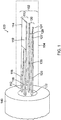
- FIG. 1 illustrates a fiber-to-waveguide optical coupler 100, according to one embodiment.
- the optical coupler 100 comprises a waveguide structure 102 surrounded by and embedded in a cladding 104.
- the waveguide structure 102 includes a first waveguide layer 110, and a second waveguide layer 120 separated from first waveguide layer 110 by a predetermined distance.
- the first waveguide layer 110 has a proximal end 112 and a distal end 114.
- the first waveguide layer 110 includes a first pair of waveguides 116, 118 that extend from proximal end 112 along a first portion of first waveguide layer 110.
- the first pair of waveguides 116, 118 each widen along a second portion of first waveguide layer 110 such that the first pair of waveguides 116, 118, merge into a single waveguide 119 toward distal end 114.
- the second waveguide layer 120 has a proximal end 122 and a distal end 124.
- the second waveguide layer 120 includes a second pair of waveguides 126, 128 that extend from proximal end 122 along a first portion of second waveguide layer 120.
- the second pair of waveguides 126, 128 each narrow along a second portion of second waveguide layer 120 to respective distal tips 127, 129 at distal end 124.
- the waveguide structure 102 is configured to couple an optical fiber 140 to an integrated photonics platform, such that an integrated photonics mode is matched to a fiber mode supported by optical fiber 140.
- the first and second waveguide layers 110, 120 can be composed of various higher index optically transmissive materials, such as silicon, silicon nitride (SiNx), silicon oxynitride (SiON), silicon carbide (SiC), diamond, silicon germanium (SiGe), germanium, gallium arsenide (GaAs), gallium nitride (GaN), gallium phosphide (GaP), lithium niobate (LiNbO 3 ), titanium dioxide (TiO 2 ), or combinations thereof.
- silicon silicon nitride
- SiON silicon oxynitride
- SiC silicon carbide
- SiGe silicon germanium
- GaAs gallium arsenide
- GaN gallium nitride
- GaP gallium phosphide
- LiNbO 3 lithium niobate
- TiO 2 titanium dioxide
- the cladding 104 can be composed of various lower index materials, such as silicon dioxide (SiO 2 ), silicon oxynitride (SiON), zinc oxide (ZnO) (used with Si waveguide or other similarly high index waveguide), aluminum oxide (Al 2 O 3 ), calcium fluoride (CaF 2 ), or combinations thereof.
- silicon dioxide SiO 2
- silicon oxynitride SiON
- zinc oxide ZnO
- Al 2 O 3 aluminum oxide
- CaF 2 calcium fluoride
- the first pair of waveguides 116, 118 can each have a thickness of about 25 nm to about 100 nm, and the second pair of waveguides 126, 128 can each have a thickness of about 25 nm to about 100 nm.
- the second waveguide layer 120 is separated from the first waveguide layer 110 by a distance of about 1 ⁇ m to about 4 ⁇ m.
- optical coupler 100 Various methods can be used to fabricate optical coupler 100, such as plasma enhanced chemical vapor deposition (PECVD), sputtering, low pressure CVD, atomic layer deposition, combinations thereof, or the like.
- PECVD plasma enhanced chemical vapor deposition
- sputtering sputtering
- low pressure CVD low pressure CVD
- atomic layer deposition atomic layer deposition, combinations thereof, or the like.
- more than two waveguide layers can be implemented to further improve efficiency of the fiber-to-waveguide optical coupler.
- Figures 2A-2I depict an exemplary method of fabricating a fiber-to-waveguide optical coupler, such as optical coupler 100. Fabrication of the optical coupler begins with a wafer substrate 210 having an upper surface 212, as shown in Figure 2A .
- the wafer substrate 210 can be formed of a first material that possesses a lower refractive index, such as silicon dioxide, for example.
- a first waveguide layer 220 is formed by depositing a second material on upper surface 212 of wafer substrate 210, as shown in Figure 2B .
- the second material has a higher refractive index than the first material.
- the second material can be silicon nitride deposited to have a thickness of about 25 nm to about 100 nm on a silicon dioxide wafer using PECVD
- a first pair of waveguides are then formed from first waveguide layer 220 by conventional lithography, dry etching, and deposition techniques. As shown in Figure 2C , a first pair of resist layers 222, 224 are formed on first waveguide layer 220 such as through resist spinning and lithography techniques. A pair of waveguides 230, 232 are then formed from first waveguide layer 220 by etching and resist removal, as depicted in Figure 2D .
- a first cladding layer 240 is then formed, by depositing the same first material as used for wafer substrate 210, over waveguides 230, 232, as depicted in Figure 2E .
- cladding layer 240 can be formed by depositing a layer of silicon dioxide having a thickness of about 2.5 ⁇ m to about 3.5 ⁇ m.
- An optional chemical mechanical planarization (CMP) process can be performed on an upper surface 242 of cladding layer 240.
- a second waveguide layer 250 is formed by depositing the second material, having the higher refractive index, over upper surface 242 of cladding layer 240, as shown in Figure 2F .
- the second material can again be silicon nitride deposited to have a thickness of about 25 nm to about 100 nm on a silicon dioxide layer using PECVD
- a second pair of waveguides are then formed from second waveguide layer 250 by conventional lithography, dry etching, and deposition techniques. As shown in Figure 2G , a pair of resist layers 252, 254 are formed on second waveguide layer 250 such as through resist spinning and lithography techniques. A pair of waveguides 260, 262 are then formed from first waveguide layer 250 by etching and resist removal, as depicted in Figure 2H .
- cladding layer 270 can be formed by depositing a layer of silicon dioxide having a thickness of about 2 ⁇ m to about 4 ⁇ m.
- Figures 3A-3C are modeled graphical representations of the simulated performance of a fiber-to-waveguide optical coupler according to the present approach.
- the fiber-to-waveguide optical coupler for the simulation included four waveguides on two layers positioned to optimize the overlap integral with a fiber mode, which is shown in Figure 3A .
- An integrated photonics waveguide mode is depicted in Figure 3B , which shows that the waveguide mode is pulled apart and expanded by having the four waveguides so that the waveguide mode more closely resembles the shape of the fiber mode.
- Figure 3C shows a side-view simulated fiber-to-waveguide transition of an optical signal from an optical fiber to the fiber-to-waveguide optical coupler.
- Figure 3C indicates that the transition of light from the fiber mode to the waveguide mode using the fiber-to-waveguide optical coupler would be about 99.17% efficient.
- FIG. 4 illustrates a fiber-to-waveguide optical coupler 300, according to an exemplary implementation.
- the optical coupler 300 comprises a waveguide structure 302 that includes a first waveguide layer 310, and a second waveguide layer 320 separated from first waveguide layer 310.
- the first waveguide layer 310 includes a first pair of waveguides 312, 314 that extend from an input end 330.
- the first pair of waveguides 312, 314 each widen toward an output end 332 such that the first pair of waveguides merge into a single waveguide 316.
- the second waveguide layer 320 includes a second pair of waveguides 322, 324 that extend from input end 330.
- the second pair of waveguides 322, 324 each narrow toward output end 332 and terminate at respective distal tips.
- the optical mode is adiabatically transitioned (second transition) into the first waveguide layer 310 toward output end 332.
- This second transition has a greater than about 99.9% efficiency.
- Figures 5A-5C are modeled graphical representations of the simulated mode profile transitions taken along optical coupler 300 of Figure 4 , from input end 330 (lines 5A) to output end 332 (lines 5C).
- the mode profile of the light is equally spaced in the waveguide layers 310, 320 at input end 330.
- the mode profile then transitions to the pair or waveguides 312, 314 in the first waveguide layer 310, as shown in Figure 5B . Thereafter, the mode profile transitions into single waveguide 316 toward output end 332, as depicted in Fig. 5C .
Landscapes
- Physics & Mathematics (AREA)
- General Physics & Mathematics (AREA)
- Optics & Photonics (AREA)
- Optical Integrated Circuits (AREA)
- Optical Couplings Of Light Guides (AREA)
Abstract
Description
- Integrated photonics offers significant advantages over fiber and free-space optics for a wide range of applications due to its ability to miniaturize optical fields while maintaining high degrees of robustness, resulting in reduced size, weight, and power consumption. Currently, one of the most significant limiting factors facing integrated photonics is the difficulty in interfacing with fiber optics. In coupling light from a fiber to a waveguide, several decibels of power are typically lost.
- In prior approaches, lensed fibers or ultra-high numerical aperture fibers are butt-coupled to inverse tapers in integrated photonics chips. The minimum total facet loss that has been achieved in this way is about 0.4 dB, which corresponds to roughly 90% coupling efficiency. However, for many applications an even higher efficiency, ideally approaching 100%, is desired.
- Thus, there is a need for a high-efficiency coupler with the flexibility to be applied to many different integrated photonics platforms.
- An optical coupler comprises a waveguide structure including a first waveguide layer having a proximal end and a distal end, the first waveguide layer including a first pair of waveguides that extend from the proximal end along a first portion of the first waveguide layer, wherein the first pair of waveguides each widen along a second portion of the first waveguide layer such that the first pair of waveguides merge into a single waveguide toward the distal end. A second waveguide layer is separated from the first waveguide layer, with the second waveguide layer having a proximal end and a distal end, the second waveguide layer including a second pair of waveguides that extend from the proximal end of the second waveguide layer along a first portion of the second waveguide layer, wherein the second pair of waveguides each narrow along a second portion of the second waveguide layer to separate distal tips at the distal end of the second waveguide layer. The waveguide structure is configured to match an integrated photonics mode to a fiber mode supported by an optical fiber.
- Features of the present invention will become apparent to those skilled in the art from the following description with reference to the drawings. Understanding that the drawings depict only typical embodiments and are not therefore to be considered limiting in scope, the invention will be described with additional specificity and detail through the use of the accompanying drawings, in which:
-
Figure 1 is a perspective side view of a fiber-to-waveguide optical coupler, according to one embodiment; -
Figures 2A-2I are end views depicting an exemplary method of fabricating a fiber-to-waveguide optical coupler; -
Figures 3A-3C are modeled graphical representations of simulated performance for a fiber-to-waveguide optical coupler, according to one implementation; -
Figure 4 is a perspective view of a fiber-to-waveguide optical coupler, according to an exemplary implementation; and -
Figures 5A-5C are modeled graphical representations of the simulated mode profile transitions for the optical coupler ofFigure 4 . - In the following detailed description, embodiments are described in sufficient detail to enable those skilled in the art to practice the invention. It is to be understood that other embodiments may be utilized without departing from the scope of the invention. The following detailed description is, therefore, not to be taken in a limiting sense.
- A high-efficiency fiber-to-waveguide coupler is described herein. In general, the fiber-to-waveguide coupler includes a multi-layer waveguide structure that matches an integrated photonics mode to the mode supported by a standard optical fiber. The mode matching of the present approach, combined with subsequent adiabatic transitions, result in a higher efficiency for coupling from a fiber mode to a waveguide mode. This mode matching can be extended to support a wide range of different material platforms.
- For example, the fiber-to-waveguide coupler can be implemented in a resonator fiber-optic gyroscope (RFOG), to direct light into and out of an optical resonator of the RFOG. The greater coupling efficiency of the fiber-to-waveguide coupler can lead to significant improvements in RFOG performance. In other implementations, the fiber-to-waveguide coupler can be employed to direct light onto chip-scale light detection and ranging (LIDAR) devices. The fiber-to-waveguide coupler can also be used as an optical interconnect for a variety of optical devices.
- In one embodiment, the fiber-to-waveguide coupler can be made by fabricating silicon nitride-on-insulator waveguides comprising two separate nitride layers, through conventional lithography, dry etching, and deposition techniques. The thickness of the two separate nitride layers, as well as the separation between them, is selected to result in a two-layer waveguide mode. Following this structure, the method of fabrication adiabatically widens and combines the two waveguides in the upper (or lower) waveguide layer, then subsequently narrows and terminates the two waveguides in the lower (or upper) waveguide layer.
- To couple light into a device, an optical fiber is positioned into alignment with the fiber-to-waveguide coupler. For example, the optical fiber can be brought into direct contact with a diced edge of a chip, at which point the fiber-to-waveguide coupler is positioned. The optical fiber can be optionally bonded to a facet of the fiber-to-waveguide coupler using index matching epoxy.
- The efficiency of the initial hand-off from the fiber mode to the waveguide mode is theoretically simulated to be greater than about 99%, and the following adiabatic transition into a single waveguide layer is theoretically simulated to be greater than about 99.9%.
- Further details of various embodiments are described hereafter with reference to the drawings.
-
Figure 1 illustrates a fiber-to-waveguide optical coupler 100, according to one embodiment. The optical coupler 100 comprises awaveguide structure 102 surrounded by and embedded in acladding 104. Thewaveguide structure 102 includes afirst waveguide layer 110, and asecond waveguide layer 120 separated fromfirst waveguide layer 110 by a predetermined distance. - The
first waveguide layer 110 has aproximal end 112 and adistal end 114. Thefirst waveguide layer 110 includes a first pair ofwaveguides proximal end 112 along a first portion offirst waveguide layer 110. The first pair ofwaveguides first waveguide layer 110 such that the first pair ofwaveguides single waveguide 119 towarddistal end 114. - The
second waveguide layer 120 has aproximal end 122 and adistal end 124. Thesecond waveguide layer 120 includes a second pair ofwaveguides proximal end 122 along a first portion ofsecond waveguide layer 120. The second pair ofwaveguides second waveguide layer 120 to respectivedistal tips distal end 124. - The
waveguide structure 102 is configured to couple anoptical fiber 140 to an integrated photonics platform, such that an integrated photonics mode is matched to a fiber mode supported byoptical fiber 140. - The first and
second waveguide layers - The
cladding 104 can be composed of various lower index materials, such as silicon dioxide (SiO2), silicon oxynitride (SiON), zinc oxide (ZnO) (used with Si waveguide or other similarly high index waveguide), aluminum oxide (Al2O3), calcium fluoride (CaF2), or combinations thereof. - The first pair of
waveguides waveguides second waveguide layer 120 is separated from thefirst waveguide layer 110 by a distance of about 1 µm to about 4 µm. - Various methods can be used to fabricate optical coupler 100, such as plasma enhanced chemical vapor deposition (PECVD), sputtering, low pressure CVD, atomic layer deposition, combinations thereof, or the like.
- In other embodiments, more than two waveguide layers can be implemented to further improve efficiency of the fiber-to-waveguide optical coupler.
-
Figures 2A-2I depict an exemplary method of fabricating a fiber-to-waveguide optical coupler, such as optical coupler 100. Fabrication of the optical coupler begins with awafer substrate 210 having anupper surface 212, as shown inFigure 2A . Thewafer substrate 210 can be formed of a first material that possesses a lower refractive index, such as silicon dioxide, for example. Next, afirst waveguide layer 220 is formed by depositing a second material onupper surface 212 ofwafer substrate 210, as shown inFigure 2B . The second material has a higher refractive index than the first material. For example, the second material can be silicon nitride deposited to have a thickness of about 25 nm to about 100 nm on a silicon dioxide wafer using PECVD - A first pair of waveguides are then formed from
first waveguide layer 220 by conventional lithography, dry etching, and deposition techniques. As shown inFigure 2C , a first pair ofresist layers first waveguide layer 220 such as through resist spinning and lithography techniques. A pair ofwaveguides first waveguide layer 220 by etching and resist removal, as depicted inFigure 2D . - A
first cladding layer 240 is then formed, by depositing the same first material as used forwafer substrate 210, overwaveguides Figure 2E . For example,cladding layer 240 can be formed by depositing a layer of silicon dioxide having a thickness of about 2.5 µm to about 3.5 µm. An optional chemical mechanical planarization (CMP) process can be performed on anupper surface 242 ofcladding layer 240. - Thereafter, a
second waveguide layer 250 is formed by depositing the second material, having the higher refractive index, overupper surface 242 ofcladding layer 240, as shown inFigure 2F . For example, the second material can again be silicon nitride deposited to have a thickness of about 25 nm to about 100 nm on a silicon dioxide layer using PECVD - A second pair of waveguides are then formed from
second waveguide layer 250 by conventional lithography, dry etching, and deposition techniques. As shown inFigure 2G , a pair of resistlayers second waveguide layer 250 such as through resist spinning and lithography techniques. A pair ofwaveguides first waveguide layer 250 by etching and resist removal, as depicted inFigure 2H . - Finally, an additional amount of the first material, such as silicon dioxide, is deposited over
waveguides second cladding layer 270, as depicted inFigure 2I . For example,cladding layer 270 can be formed by depositing a layer of silicon dioxide having a thickness of about 2 µm to about 4 µm. -
Figures 3A-3C are modeled graphical representations of the simulated performance of a fiber-to-waveguide optical coupler according to the present approach. The fiber-to-waveguide optical coupler for the simulation included four waveguides on two layers positioned to optimize the overlap integral with a fiber mode, which is shown inFigure 3A . An integrated photonics waveguide mode is depicted inFigure 3B , which shows that the waveguide mode is pulled apart and expanded by having the four waveguides so that the waveguide mode more closely resembles the shape of the fiber mode. -
Figure 3C shows a side-view simulated fiber-to-waveguide transition of an optical signal from an optical fiber to the fiber-to-waveguide optical coupler. The fiber mode was injected at the left end of the graph at x = 0, and an abrupt transition for the four- waveguide structure of the coupler was located at about x = 1 micron.Figure 3C indicates that the transition of light from the fiber mode to the waveguide mode using the fiber-to-waveguide optical coupler would be about 99.17% efficient. -
Figure 4 illustrates a fiber-to-waveguide optical coupler 300, according to an exemplary implementation. The optical coupler 300 comprises awaveguide structure 302 that includes a first waveguide layer 310, and asecond waveguide layer 320 separated from first waveguide layer 310. The first waveguide layer 310 includes a first pair ofwaveguides input end 330. The first pair ofwaveguides output end 332 such that the first pair of waveguides merge into asingle waveguide 316. Thesecond waveguide layer 320 includes a second pair ofwaveguides input end 330. The second pair ofwaveguides output end 332 and terminate at respective distal tips. - Following the fiber-to-waveguide transition (first transition) at
input end 330 of optical coupler 300, the optical mode is adiabatically transitioned (second transition) into the first waveguide layer 310 towardoutput end 332. This second transition has a greater than about 99.9% efficiency. -
Figures 5A-5C are modeled graphical representations of the simulated mode profile transitions taken along optical coupler 300 ofFigure 4 , from input end 330 (lines 5A) to output end 332 (lines 5C). As shown inFigure 5A , the mode profile of the light is equally spaced in the waveguide layers 310, 320 atinput end 330. The mode profile then transitions to the pair orwaveguides Figure 5B . Thereafter, the mode profile transitions intosingle waveguide 316 towardoutput end 332, as depicted inFig. 5C . -
- Example 1 includes an optical coupler, comprising: a waveguide structure comprising a first waveguide layer having a proximal end and a distal end, the first waveguide layer including a first pair of waveguides that extend from the proximal end along a first portion of the first waveguide layer, wherein the first pair of waveguides each widen along a second portion of the first waveguide layer such that the first pair of waveguides merge into a single waveguide toward the distal end; and a second waveguide layer separated from the first waveguide layer, the second waveguide layer having a proximal end and a distal end, the second waveguide layer including a second pair of waveguides that extend from the proximal end of the second waveguide layer along a first portion of the second waveguide layer, wherein the second pair of waveguides each narrow along a second portion of the second waveguide layer to separate distal tips at the distal end of the second waveguide layer; wherein the waveguide structure is configured to match an integrated photonics mode to a fiber mode supported by an optical fiber.
- Example 2 includes the optical coupler of Example 1, wherein the first and second pairs of waveguides comprise a high index optically transmissive material.
- Example 3 includes the optical coupler of any of Examples 1-2, wherein the first and second pairs of waveguides comprise silicon, silicon nitride, silicon oxynitride, silicon carbide, diamond, silicon germanium, germanium, gallium arsenide, gallium nitride, gallium phosphide, lithium niobate, titanium dioxide, or combinations thereof.
- Example 4 includes the optical coupler of any of Examples 1-3, wherein the first pair of waveguides have a thickness of about 25 nm to about 100 nm.
- Example 5 includes the optical coupler of any of Examples 1-4, wherein the second pair of waveguides have a thickness of about 25 nm to about 100 nm.
- Example 6 includes the optical coupler of any of Examples 1-5, wherein the second waveguide layer is separated from the first waveguide layer by a distance of about 2.5 µm to about 3.5 µm.
- Example 7 includes the optical coupler of any of Examples 1-6, wherein the first and second waveguide layers are embedded in a cladding.
- Example 8 includes the optical coupler of Example 7, wherein the cladding comprises a low index material.
- Example 9 includes the optical coupler of any of Examples 7-8, wherein the cladding comprises silicon dioxide, silicon oxynitride, zinc oxide, aluminum oxide, calcium fluoride, or combinations thereof.
- Example 10 includes a method of fabricating an optical coupler, the method comprising: providing a wafer substrate having an upper surface, the wafer substrate formed of a first material having a first refractive index; forming a first waveguide layer of a second material on the upper surface of the wafer substrate, the second material having a second refractive index that is higher than the first refractive index; removing portions of the second material from the first waveguide layer to form a first pair of waveguides along the first waveguide layer; forming a first cladding layer of the first material over the first pair of waveguides; forming a second waveguide layer of the second material over the first cladding layer; removing portions of the second material from the second waveguide layer to form a second pair of waveguides along the second waveguide layer; and forming a second cladding layer of the first material over the second pair of waveguides; wherein the first pair of waveguides are formed to widen along a portion of the first waveguide layer such that the first pair of waveguides merge into a single waveguide toward a distal end of the first waveguide layer; wherein the second pair of waveguides are formed to narrow along a portion of the second waveguide layer to separate distal tips at a distal end of the second waveguide layer.
- Example 11 includes the method of Example 10, wherein the first material comprises silicon dioxide, silicon oxynitride, zinc oxide, aluminum oxide, calcium fluoride, or combinations thereof.
- Example 12 includes the method of any of Examples 10-11, wherein the second material comprises silicon, silicon nitride, silicon oxynitride, silicon carbide, diamond, silicon germanium, germanium, gallium arsenide, gallium nitride, gallium phosphide, lithium niobate, titanium dioxide, or combinations thereof.
- Example 13 includes the method of any of Examples 10-12, wherein the first pair of waveguides is formed to have a thickness of about 25 nm to about 100 nm.
- Example 14 includes the method of any of Examples 10-13, wherein the second pair of waveguides is formed to have a thickness of about 25 nm to about 100 nm.
- Example 15 includes the method of any of Examples 10-14, wherein the second waveguide layer is separated from the first waveguide layer by a distance of about 2.5 µm to about 3.5 µm.
- Example 16 includes the method of any of Examples 10-15, wherein the first and second waveguide layers are formed by a process comprising plasma enhanced chemical vapor deposition, sputtering, low pressure chemical vapor deposition, atomic layer deposition, or combinations thereof.
- Example 17 includes the method of any of Examples 10-16, wherein the first and second cladding layers are formed by a process comprising plasma enhanced chemical vapor deposition, sputtering, low pressure chemical vapor deposition, atomic layer deposition, or combinations thereof.
- Example 18 includes the method of any of Examples 10-17, wherein the portions of the second material are removed from the first and second waveguide layers by a process comprising a lithography-based procedure, followed by dry etching.
- The present invention may be embodied in other specific forms without departing from its essential characteristics. The described embodiments are to be considered in all respects only as illustrative and not restrictive. The scope of the invention is therefore indicated by the appended claims rather than by the foregoing description. All changes that come within the meaning and range of equivalency of the claims are to be embraced within their scope.
Claims (10)
- An optical coupler, comprising:a waveguide structure comprising:a first waveguide layer having a proximal end and a distal end, the first waveguide layer including a first pair of waveguides that extend from the proximal end along a first portion of the first waveguide layer, wherein the first pair of waveguides each widen along a second portion of the first waveguide layer such that the first pair of waveguides merge into a single waveguide toward the distal end; anda second waveguide layer separated from the first waveguide layer, the second waveguide layer having a proximal end and a distal end, the second waveguide layer including a second pair of waveguides that extend from the proximal end of the second waveguide layer along a first portion of the second waveguide layer, wherein the second pair of waveguides each narrow along a second portion of the second waveguide layer to separate distal tips at the distal end of the second waveguide layer;wherein the waveguide structure is configured to match an integrated photonics mode to a fiber mode supported by an optical fiber.
- The optical coupler of claim 1, wherein the first and second pairs of waveguides comprise a high index optically transmissive material.
- The optical coupler of claim 1, wherein the first and second pairs of waveguides comprise silicon, silicon nitride, silicon oxynitride, silicon carbide, diamond, silicon germanium, germanium, gallium arsenide, gallium nitride, gallium phosphide, lithium niobate, titanium dioxide, or combinations thereof.
- The optical coupler of claim 1, wherein the first pair of waveguides have a thickness of about 25 nm to about 100 nm.
- The optical coupler of claim 1, wherein the second pair of waveguides have a thickness of about 25 nm to about 100 nm.
- The optical coupler of claim 1, wherein the second waveguide layer is separated from the first waveguide layer by a distance of about 2.5 µm to about 3.5 µm.
- The optical coupler of claim 1, wherein the first and second waveguide layers are embedded in a cladding.
- The optical coupler of claim 7, wherein the cladding comprises a low index material.
- The optical coupler of claim 7, wherein the cladding comprises silicon dioxide, silicon oxynitride, zinc oxide, aluminum oxide, calcium fluoride, or combinations thereof.
- A method of fabricating an optical coupler, the method comprising:providing a wafer substrate having an upper surface, the wafer substrate formed of a first material having a first refractive index;forming a first waveguide layer of a second material on the upper surface of the wafer substrate, the second material having a second refractive index that is higher than the first refractive index;removing portions of the second material from the first waveguide layer to form a first pair of waveguides along the first waveguide layer;forming a first cladding layer of the first material over the first pair of waveguides;forming a second waveguide layer of the second material over the first cladding layer;removing portions of the second material from the second waveguide layer to form a second pair of waveguides along the second waveguide layer; andforming a second cladding layer of the first material over the second pair of waveguides;wherein the first pair of waveguides are formed to widen along a portion of the first waveguide layer such that the first pair of waveguides merge into a single waveguide toward a distal end of the first waveguide layer;wherein the second pair of waveguides are formed to narrow along a portion of the second waveguide layer to separate distal tips at a distal end of the second waveguide layer.
Applications Claiming Priority (1)
| Application Number | Priority Date | Filing Date | Title |
|---|---|---|---|
| US16/223,548 US10534136B1 (en) | 2018-12-18 | 2018-12-18 | High-efficiency fiber-to-waveguide coupler |
Publications (2)
| Publication Number | Publication Date |
|---|---|
| EP3671298A1 true EP3671298A1 (en) | 2020-06-24 |
| EP3671298B1 EP3671298B1 (en) | 2022-04-06 |
Family
ID=68886972
Family Applications (1)
| Application Number | Title | Priority Date | Filing Date |
|---|---|---|---|
| EP19215444.1A Active EP3671298B1 (en) | 2018-12-18 | 2019-12-11 | High-efficiency fiber-to-waveguide coupler |
Country Status (2)
| Country | Link |
|---|---|
| US (1) | US10534136B1 (en) |
| EP (1) | EP3671298B1 (en) |
Cited By (2)
| Publication number | Priority date | Publication date | Assignee | Title |
|---|---|---|---|---|
| WO2023167920A1 (en) * | 2022-03-01 | 2023-09-07 | Marvell Asia Pte Ltd | Array-based edge coupler for optical input/output |
| EP4379436A1 (en) * | 2022-12-01 | 2024-06-05 | Xanadu Quantum Technologies Inc. | Apparatus for optical coupler |
Families Citing this family (10)
| Publication number | Priority date | Publication date | Assignee | Title |
|---|---|---|---|---|
| US11175140B2 (en) * | 2019-09-10 | 2021-11-16 | Honeywell International Inc. | Resonator fiber optic gyroscope with integrated photonics interface |
| US11204469B1 (en) * | 2020-06-01 | 2021-12-21 | Honeywell International Inc. | Apparatus for high-efficiency fiber-to-chip coupling and mode-conversion to integrated photonics platform |
| US11016253B1 (en) * | 2020-06-08 | 2021-05-25 | Honeywell International Inc. | Adiabatic waveguide couplers with ultra-low back-reflection |
| CN112097754B (en) * | 2020-09-14 | 2022-05-27 | 浙江大学 | Lithium niobate and SU-8 hybrid integrated hollow-core photonic crystal fiber optic gyroscope |
| US11662523B2 (en) * | 2021-01-19 | 2023-05-30 | Globalfoundries U.S. Inc. | Edge couplers in the back-end-of-line stack of a photonics chip |
| US11733458B2 (en) * | 2021-10-04 | 2023-08-22 | Globalfoundries U.S. Inc. | Edge couplers with confining features |
| CN114384633B (en) * | 2022-01-21 | 2024-05-24 | 合肥知宇芯光科技有限公司 | Horizontal coupler for optical signal transmission between rectangular core few-mode optical fiber and chip |
| US12541061B2 (en) * | 2022-07-29 | 2026-02-03 | Avago Technologies International Sales Pte. Limited | Diamond spot size converter for fiber edge coupling |
| US12105327B2 (en) | 2022-12-05 | 2024-10-01 | Honeywell International Inc. | Resonator with at least two cores and gyroscope applications thereof |
| CN116661060B (en) * | 2023-07-28 | 2023-10-31 | 中天通信技术有限公司 | End face coupler and optical module |
Citations (5)
| Publication number | Priority date | Publication date | Assignee | Title |
|---|---|---|---|---|
| US20030035633A1 (en) * | 2001-05-08 | 2003-02-20 | Agarwal Anuradha M. | Vertically and laterally confined 3D optical coupler |
| US8208768B2 (en) * | 2009-10-26 | 2012-06-26 | United Microelectronics Corp. | Focusing member and optoelectronic device |
| US20120230635A1 (en) * | 2009-09-28 | 2012-09-13 | Haruhiko Yoshida | Optical coupling device and optical coupling-branching device |
| US20150247974A1 (en) * | 2014-02-28 | 2015-09-03 | Teraxion Inc. | Spot-size converter for optical mode conversion and coupling between two waveguides |
| US20160356960A1 (en) * | 2015-06-04 | 2016-12-08 | Coriant Advanced Technology, LLC | Edge Coupler |
Family Cites Families (15)
| Publication number | Priority date | Publication date | Assignee | Title |
|---|---|---|---|---|
| SE509171C2 (en) * | 1997-03-03 | 1998-12-14 | Ericsson Telefon Ab L M | Optical waveguide |
| GB0122425D0 (en) * | 2001-09-17 | 2001-11-07 | Univ Nanyang | An optical coupling mount |
| GB0208255D0 (en) | 2002-04-10 | 2002-05-22 | Imec Inter Uni Micro Electr | Photonic crystal based fiber-to-waveguide coupler for polarisation independent photonic integrated circuits |
| WO2005017588A1 (en) * | 2003-08-19 | 2005-02-24 | Ignis Technologies As | Integrated optics spot size converter and manufacturing method |
| US7643710B1 (en) | 2008-09-17 | 2010-01-05 | Intel Corporation | Method and apparatus for efficient coupling between silicon photonic chip and optical fiber |
| WO2012049273A1 (en) | 2010-10-14 | 2012-04-19 | Rwth Aachen | Laser to chip coupler |
| JP6140923B2 (en) * | 2011-12-28 | 2017-06-07 | 富士通株式会社 | Spot size converter, optical transmitter, optical receiver, optical transceiver, and manufacturing method of spot size converter |
| US20130230274A1 (en) | 2012-03-05 | 2013-09-05 | Gregory Alan Fish | Photonic flexible interconnect |
| KR20130112548A (en) * | 2012-04-04 | 2013-10-14 | 한국전자통신연구원 | Spot size converter and manufacturing method of the same |
| JP6346177B2 (en) * | 2013-06-21 | 2018-06-20 | 古河電気工業株式会社 | Spot size conversion optical waveguide |
| US9164235B1 (en) | 2014-07-02 | 2015-10-20 | Cisco Technology, Inc. | Dual tip optical coupler |
| US10996401B2 (en) | 2016-06-30 | 2021-05-04 | Mellanox Technologies, Ltd. | Method and apparatus for optical coupling of optical signals for a photonic integrated circuit |
| US20180011244A1 (en) | 2016-07-11 | 2018-01-11 | University Of Maryland | Generation of arbitrary optical filtering function using complex bragg gratings |
| US10605988B2 (en) * | 2016-08-02 | 2020-03-31 | Telefonaktiebolaget Lm Ericsson (Publ) | Optical beam spot size converter |
| WO2018130285A1 (en) | 2017-01-12 | 2018-07-19 | Telefonaktiebolaget Lm Ericsson (Publ) | Apparatus and method for coupling light |
-
2018
- 2018-12-18 US US16/223,548 patent/US10534136B1/en active Active
-
2019
- 2019-12-11 EP EP19215444.1A patent/EP3671298B1/en active Active
Patent Citations (7)
| Publication number | Priority date | Publication date | Assignee | Title |
|---|---|---|---|---|
| US20030035633A1 (en) * | 2001-05-08 | 2003-02-20 | Agarwal Anuradha M. | Vertically and laterally confined 3D optical coupler |
| US7120335B2 (en) * | 2001-05-08 | 2006-10-10 | Massachusetts Institute Of Technology | Vertically and laterally confined 3D optical coupler |
| US20120230635A1 (en) * | 2009-09-28 | 2012-09-13 | Haruhiko Yoshida | Optical coupling device and optical coupling-branching device |
| US8744225B2 (en) * | 2009-09-28 | 2014-06-03 | Kabushiki Kaisha Toshiba | Optical coupling device and optical coupling-branching device |
| US8208768B2 (en) * | 2009-10-26 | 2012-06-26 | United Microelectronics Corp. | Focusing member and optoelectronic device |
| US20150247974A1 (en) * | 2014-02-28 | 2015-09-03 | Teraxion Inc. | Spot-size converter for optical mode conversion and coupling between two waveguides |
| US20160356960A1 (en) * | 2015-06-04 | 2016-12-08 | Coriant Advanced Technology, LLC | Edge Coupler |
Non-Patent Citations (1)
| Title |
|---|
| S H TAO ET AL: "Improving coupling efficiency of fiber-waveguide coupling with a double-tip coupler", OPT. EXPRESS, vol. 16, no. 25, 2 December 2008 (2008-12-02), pages 20804 - 20808, XP055691406 * |
Cited By (3)
| Publication number | Priority date | Publication date | Assignee | Title |
|---|---|---|---|---|
| WO2023167920A1 (en) * | 2022-03-01 | 2023-09-07 | Marvell Asia Pte Ltd | Array-based edge coupler for optical input/output |
| US12541065B2 (en) | 2022-03-01 | 2026-02-03 | Marvell Asia Pte Ltd | Array-based edge coupler for optical input/output |
| EP4379436A1 (en) * | 2022-12-01 | 2024-06-05 | Xanadu Quantum Technologies Inc. | Apparatus for optical coupler |
Also Published As
| Publication number | Publication date |
|---|---|
| EP3671298B1 (en) | 2022-04-06 |
| US10534136B1 (en) | 2020-01-14 |
Similar Documents
| Publication | Publication Date | Title |
|---|---|---|
| EP3671298B1 (en) | High-efficiency fiber-to-waveguide coupler | |
| EP3919952B1 (en) | Apparatus for high-efficiency fiber-to-chip coupling and mode-conversion to integrated photonics platform | |
| US8000565B2 (en) | Buried dual taper waveguide for passive alignment and photonic integration | |
| CN109642985B (en) | Mode converter and method of making the same | |
| EP3296806B1 (en) | Acoustic ridge or rib waveguides in low-loss integrated optical platforms | |
| US6911672B2 (en) | Method and apparatus for preparing a plurality of dice in wafers | |
| CN106164722B (en) | Edge coupled device fabrication | |
| EP3123218B1 (en) | Edge coupling using adiabatically tapered waveguides | |
| EP3451032B1 (en) | Smooth waveguide structures and manfacturing methods | |
| US10627654B2 (en) | Etchless acoustic waveguiding in integrated acousto-optic waveguides | |
| CN102159975A (en) | Method and apparatus for efficient coupling between silicon photonic chip and optical fiber | |
| EP3296693A1 (en) | Double-layer high-confinement acousto-optic waveguide | |
| US20050054130A1 (en) | Maskless Fabrication of waveguide mirrors | |
| EP3923047B1 (en) | Adiabatic waveguide couplers with ultra-low back-reflection | |
| CN112180502A (en) | Silicon-based optical coupling structure, silicon-based monolithic integrated optical device and manufacturing method thereof | |
| CN114265147B (en) | Optical communication band wide bandwidth and high efficiency horizontal end coupler and manufacturing method thereof | |
| EP3531177A1 (en) | Optical chip for coupling light and fabrication method | |
| US20050129366A1 (en) | Graded index optical coupler | |
| JP2820202B2 (en) | Manufacturing method of spot size converter | |
| RU2712985C1 (en) | Mode converter device | |
| JP2025128968A (en) | Optical Waveguide Element | |
| Lützow et al. | Vertical optical interfacing of Silicon waveguides |
Legal Events
| Date | Code | Title | Description |
|---|---|---|---|
| PUAI | Public reference made under article 153(3) epc to a published international application that has entered the european phase |
Free format text: ORIGINAL CODE: 0009012 |
|
| STAA | Information on the status of an ep patent application or granted ep patent |
Free format text: STATUS: THE APPLICATION HAS BEEN PUBLISHED |
|
| AK | Designated contracting states |
Kind code of ref document: A1 Designated state(s): AL AT BE BG CH CY CZ DE DK EE ES FI FR GB GR HR HU IE IS IT LI LT LU LV MC MK MT NL NO PL PT RO RS SE SI SK SM TR |
|
| AX | Request for extension of the european patent |
Extension state: BA ME |
|
| STAA | Information on the status of an ep patent application or granted ep patent |
Free format text: STATUS: REQUEST FOR EXAMINATION WAS MADE |
|
| 17P | Request for examination filed |
Effective date: 20200706 |
|
| RBV | Designated contracting states (corrected) |
Designated state(s): AL AT BE BG CH CY CZ DE DK EE ES FI FR GB GR HR HU IE IS IT LI LT LU LV MC MK MT NL NO PL PT RO RS SE SI SK SM TR |
|
| GRAP | Despatch of communication of intention to grant a patent |
Free format text: ORIGINAL CODE: EPIDOSNIGR1 |
|
| STAA | Information on the status of an ep patent application or granted ep patent |
Free format text: STATUS: GRANT OF PATENT IS INTENDED |
|
| INTG | Intention to grant announced |
Effective date: 20211210 |
|
| GRAS | Grant fee paid |
Free format text: ORIGINAL CODE: EPIDOSNIGR3 |
|
| GRAA | (expected) grant |
Free format text: ORIGINAL CODE: 0009210 |
|
| STAA | Information on the status of an ep patent application or granted ep patent |
Free format text: STATUS: THE PATENT HAS BEEN GRANTED |
|
| AK | Designated contracting states |
Kind code of ref document: B1 Designated state(s): AL AT BE BG CH CY CZ DE DK EE ES FI FR GB GR HR HU IE IS IT LI LT LU LV MC MK MT NL NO PL PT RO RS SE SI SK SM TR |
|
| REG | Reference to a national code |
Ref country code: GB Ref legal event code: FG4D |
|
| REG | Reference to a national code |
Ref country code: CH Ref legal event code: EP |
|
| REG | Reference to a national code |
Ref country code: AT Ref legal event code: REF Ref document number: 1481887 Country of ref document: AT Kind code of ref document: T Effective date: 20220415 |
|
| REG | Reference to a national code |
Ref country code: IE Ref legal event code: FG4D |
|
| REG | Reference to a national code |
Ref country code: DE Ref legal event code: R096 Ref document number: 602019013377 Country of ref document: DE |
|
| REG | Reference to a national code |
Ref country code: LT Ref legal event code: MG9D |
|
| REG | Reference to a national code |
Ref country code: NL Ref legal event code: MP Effective date: 20220406 |
|
| REG | Reference to a national code |
Ref country code: AT Ref legal event code: MK05 Ref document number: 1481887 Country of ref document: AT Kind code of ref document: T Effective date: 20220406 |
|
| PG25 | Lapsed in a contracting state [announced via postgrant information from national office to epo] |
Ref country code: NL Free format text: LAPSE BECAUSE OF FAILURE TO SUBMIT A TRANSLATION OF THE DESCRIPTION OR TO PAY THE FEE WITHIN THE PRESCRIBED TIME-LIMIT Effective date: 20220406 |
|
| PG25 | Lapsed in a contracting state [announced via postgrant information from national office to epo] |
Ref country code: SE Free format text: LAPSE BECAUSE OF FAILURE TO SUBMIT A TRANSLATION OF THE DESCRIPTION OR TO PAY THE FEE WITHIN THE PRESCRIBED TIME-LIMIT Effective date: 20220406 Ref country code: PT Free format text: LAPSE BECAUSE OF FAILURE TO SUBMIT A TRANSLATION OF THE DESCRIPTION OR TO PAY THE FEE WITHIN THE PRESCRIBED TIME-LIMIT Effective date: 20220808 Ref country code: NO Free format text: LAPSE BECAUSE OF FAILURE TO SUBMIT A TRANSLATION OF THE DESCRIPTION OR TO PAY THE FEE WITHIN THE PRESCRIBED TIME-LIMIT Effective date: 20220706 Ref country code: LT Free format text: LAPSE BECAUSE OF FAILURE TO SUBMIT A TRANSLATION OF THE DESCRIPTION OR TO PAY THE FEE WITHIN THE PRESCRIBED TIME-LIMIT Effective date: 20220406 Ref country code: HR Free format text: LAPSE BECAUSE OF FAILURE TO SUBMIT A TRANSLATION OF THE DESCRIPTION OR TO PAY THE FEE WITHIN THE PRESCRIBED TIME-LIMIT Effective date: 20220406 Ref country code: GR Free format text: LAPSE BECAUSE OF FAILURE TO SUBMIT A TRANSLATION OF THE DESCRIPTION OR TO PAY THE FEE WITHIN THE PRESCRIBED TIME-LIMIT Effective date: 20220707 Ref country code: FI Free format text: LAPSE BECAUSE OF FAILURE TO SUBMIT A TRANSLATION OF THE DESCRIPTION OR TO PAY THE FEE WITHIN THE PRESCRIBED TIME-LIMIT Effective date: 20220406 Ref country code: ES Free format text: LAPSE BECAUSE OF FAILURE TO SUBMIT A TRANSLATION OF THE DESCRIPTION OR TO PAY THE FEE WITHIN THE PRESCRIBED TIME-LIMIT Effective date: 20220406 Ref country code: BG Free format text: LAPSE BECAUSE OF FAILURE TO SUBMIT A TRANSLATION OF THE DESCRIPTION OR TO PAY THE FEE WITHIN THE PRESCRIBED TIME-LIMIT Effective date: 20220706 Ref country code: AT Free format text: LAPSE BECAUSE OF FAILURE TO SUBMIT A TRANSLATION OF THE DESCRIPTION OR TO PAY THE FEE WITHIN THE PRESCRIBED TIME-LIMIT Effective date: 20220406 |
|
| PG25 | Lapsed in a contracting state [announced via postgrant information from national office to epo] |
Ref country code: RS Free format text: LAPSE BECAUSE OF FAILURE TO SUBMIT A TRANSLATION OF THE DESCRIPTION OR TO PAY THE FEE WITHIN THE PRESCRIBED TIME-LIMIT Effective date: 20220406 Ref country code: PL Free format text: LAPSE BECAUSE OF FAILURE TO SUBMIT A TRANSLATION OF THE DESCRIPTION OR TO PAY THE FEE WITHIN THE PRESCRIBED TIME-LIMIT Effective date: 20220406 Ref country code: LV Free format text: LAPSE BECAUSE OF FAILURE TO SUBMIT A TRANSLATION OF THE DESCRIPTION OR TO PAY THE FEE WITHIN THE PRESCRIBED TIME-LIMIT Effective date: 20220406 Ref country code: IS Free format text: LAPSE BECAUSE OF FAILURE TO SUBMIT A TRANSLATION OF THE DESCRIPTION OR TO PAY THE FEE WITHIN THE PRESCRIBED TIME-LIMIT Effective date: 20220806 |
|
| REG | Reference to a national code |
Ref country code: DE Ref legal event code: R097 Ref document number: 602019013377 Country of ref document: DE |
|
| PG25 | Lapsed in a contracting state [announced via postgrant information from national office to epo] |
Ref country code: SM Free format text: LAPSE BECAUSE OF FAILURE TO SUBMIT A TRANSLATION OF THE DESCRIPTION OR TO PAY THE FEE WITHIN THE PRESCRIBED TIME-LIMIT Effective date: 20220406 Ref country code: SK Free format text: LAPSE BECAUSE OF FAILURE TO SUBMIT A TRANSLATION OF THE DESCRIPTION OR TO PAY THE FEE WITHIN THE PRESCRIBED TIME-LIMIT Effective date: 20220406 Ref country code: RO Free format text: LAPSE BECAUSE OF FAILURE TO SUBMIT A TRANSLATION OF THE DESCRIPTION OR TO PAY THE FEE WITHIN THE PRESCRIBED TIME-LIMIT Effective date: 20220406 Ref country code: EE Free format text: LAPSE BECAUSE OF FAILURE TO SUBMIT A TRANSLATION OF THE DESCRIPTION OR TO PAY THE FEE WITHIN THE PRESCRIBED TIME-LIMIT Effective date: 20220406 Ref country code: DK Free format text: LAPSE BECAUSE OF FAILURE TO SUBMIT A TRANSLATION OF THE DESCRIPTION OR TO PAY THE FEE WITHIN THE PRESCRIBED TIME-LIMIT Effective date: 20220406 Ref country code: CZ Free format text: LAPSE BECAUSE OF FAILURE TO SUBMIT A TRANSLATION OF THE DESCRIPTION OR TO PAY THE FEE WITHIN THE PRESCRIBED TIME-LIMIT Effective date: 20220406 |
|
| PLBE | No opposition filed within time limit |
Free format text: ORIGINAL CODE: 0009261 |
|
| STAA | Information on the status of an ep patent application or granted ep patent |
Free format text: STATUS: NO OPPOSITION FILED WITHIN TIME LIMIT |
|
| 26N | No opposition filed |
Effective date: 20230110 |
|
| PG25 | Lapsed in a contracting state [announced via postgrant information from national office to epo] |
Ref country code: AL Free format text: LAPSE BECAUSE OF FAILURE TO SUBMIT A TRANSLATION OF THE DESCRIPTION OR TO PAY THE FEE WITHIN THE PRESCRIBED TIME-LIMIT Effective date: 20220406 |
|
| PG25 | Lapsed in a contracting state [announced via postgrant information from national office to epo] |
Ref country code: SI Free format text: LAPSE BECAUSE OF FAILURE TO SUBMIT A TRANSLATION OF THE DESCRIPTION OR TO PAY THE FEE WITHIN THE PRESCRIBED TIME-LIMIT Effective date: 20220406 |
|
| REG | Reference to a national code |
Ref country code: DE Ref legal event code: R119 Ref document number: 602019013377 Country of ref document: DE |
|
| P01 | Opt-out of the competence of the unified patent court (upc) registered |
Effective date: 20230525 |
|
| REG | Reference to a national code |
Ref country code: CH Ref legal event code: PL |
|
| REG | Reference to a national code |
Ref country code: BE Ref legal event code: MM Effective date: 20221231 |
|
| PG25 | Lapsed in a contracting state [announced via postgrant information from national office to epo] |
Ref country code: LU Free format text: LAPSE BECAUSE OF NON-PAYMENT OF DUE FEES Effective date: 20221211 |
|
| PG25 | Lapsed in a contracting state [announced via postgrant information from national office to epo] |
Ref country code: LI Free format text: LAPSE BECAUSE OF NON-PAYMENT OF DUE FEES Effective date: 20221231 Ref country code: IE Free format text: LAPSE BECAUSE OF NON-PAYMENT OF DUE FEES Effective date: 20221211 Ref country code: DE Free format text: LAPSE BECAUSE OF NON-PAYMENT OF DUE FEES Effective date: 20230701 Ref country code: CH Free format text: LAPSE BECAUSE OF NON-PAYMENT OF DUE FEES Effective date: 20221231 |
|
| PG25 | Lapsed in a contracting state [announced via postgrant information from national office to epo] |
Ref country code: BE Free format text: LAPSE BECAUSE OF NON-PAYMENT OF DUE FEES Effective date: 20221231 |
|
| PG25 | Lapsed in a contracting state [announced via postgrant information from national office to epo] |
Ref country code: IT Free format text: LAPSE BECAUSE OF FAILURE TO SUBMIT A TRANSLATION OF THE DESCRIPTION OR TO PAY THE FEE WITHIN THE PRESCRIBED TIME-LIMIT Effective date: 20220406 |
|
| PG25 | Lapsed in a contracting state [announced via postgrant information from national office to epo] |
Ref country code: HU Free format text: LAPSE BECAUSE OF FAILURE TO SUBMIT A TRANSLATION OF THE DESCRIPTION OR TO PAY THE FEE WITHIN THE PRESCRIBED TIME-LIMIT; INVALID AB INITIO Effective date: 20191211 |
|
| PG25 | Lapsed in a contracting state [announced via postgrant information from national office to epo] |
Ref country code: CY Free format text: LAPSE BECAUSE OF FAILURE TO SUBMIT A TRANSLATION OF THE DESCRIPTION OR TO PAY THE FEE WITHIN THE PRESCRIBED TIME-LIMIT Effective date: 20220406 |
|
| PG25 | Lapsed in a contracting state [announced via postgrant information from national office to epo] |
Ref country code: MK Free format text: LAPSE BECAUSE OF FAILURE TO SUBMIT A TRANSLATION OF THE DESCRIPTION OR TO PAY THE FEE WITHIN THE PRESCRIBED TIME-LIMIT Effective date: 20220406 |
|
| PG25 | Lapsed in a contracting state [announced via postgrant information from national office to epo] |
Ref country code: MC Free format text: LAPSE BECAUSE OF FAILURE TO SUBMIT A TRANSLATION OF THE DESCRIPTION OR TO PAY THE FEE WITHIN THE PRESCRIBED TIME-LIMIT Effective date: 20220406 |
|
| PG25 | Lapsed in a contracting state [announced via postgrant information from national office to epo] |
Ref country code: TR Free format text: LAPSE BECAUSE OF FAILURE TO SUBMIT A TRANSLATION OF THE DESCRIPTION OR TO PAY THE FEE WITHIN THE PRESCRIBED TIME-LIMIT Effective date: 20220406 Ref country code: MC Free format text: LAPSE BECAUSE OF FAILURE TO SUBMIT A TRANSLATION OF THE DESCRIPTION OR TO PAY THE FEE WITHIN THE PRESCRIBED TIME-LIMIT Effective date: 20220406 |
|
| GBPC | Gb: european patent ceased through non-payment of renewal fee |
Effective date: 20231211 |
|
| PG25 | Lapsed in a contracting state [announced via postgrant information from national office to epo] |
Ref country code: MT Free format text: LAPSE BECAUSE OF FAILURE TO SUBMIT A TRANSLATION OF THE DESCRIPTION OR TO PAY THE FEE WITHIN THE PRESCRIBED TIME-LIMIT Effective date: 20220406 |
|
| PG25 | Lapsed in a contracting state [announced via postgrant information from national office to epo] |
Ref country code: GB Free format text: LAPSE BECAUSE OF NON-PAYMENT OF DUE FEES Effective date: 20231211 |
|
| PG25 | Lapsed in a contracting state [announced via postgrant information from national office to epo] |
Ref country code: GB Free format text: LAPSE BECAUSE OF NON-PAYMENT OF DUE FEES Effective date: 20231211 |
|
| PG25 | Lapsed in a contracting state [announced via postgrant information from national office to epo] |
Ref country code: BG Free format text: LAPSE BECAUSE OF FAILURE TO SUBMIT A TRANSLATION OF THE DESCRIPTION OR TO PAY THE FEE WITHIN THE PRESCRIBED TIME-LIMIT Effective date: 20220406 |
|
| PG25 | Lapsed in a contracting state [announced via postgrant information from national office to epo] |
Ref country code: BG Free format text: LAPSE BECAUSE OF FAILURE TO SUBMIT A TRANSLATION OF THE DESCRIPTION OR TO PAY THE FEE WITHIN THE PRESCRIBED TIME-LIMIT Effective date: 20220406 |
|
| PGFP | Annual fee paid to national office [announced via postgrant information from national office to epo] |
Ref country code: FR Payment date: 20251223 Year of fee payment: 7 |