EP3668282A1 - Conductive traces - Google Patents
Conductive traces Download PDFInfo
- Publication number
- EP3668282A1 EP3668282A1 EP18211577.4A EP18211577A EP3668282A1 EP 3668282 A1 EP3668282 A1 EP 3668282A1 EP 18211577 A EP18211577 A EP 18211577A EP 3668282 A1 EP3668282 A1 EP 3668282A1
- Authority
- EP
- European Patent Office
- Prior art keywords
- conductive trace
- substrate
- sub
- elastomeric substrate
- conductive
- Prior art date
- Legal status (The legal status is an assumption and is not a legal conclusion. Google has not performed a legal analysis and makes no representation as to the accuracy of the status listed.)
- Pending
Links
- 239000000758 substrate Substances 0.000 claims abstract description 81
- 238000000034 method Methods 0.000 claims abstract description 29
- 239000000463 material Substances 0.000 claims abstract description 25
- 238000010438 heat treatment Methods 0.000 claims abstract description 5
- 238000000151 deposition Methods 0.000 claims abstract description 4
- 238000003856 thermoforming Methods 0.000 claims description 10
- 239000002245 particle Substances 0.000 claims description 8
- OKTJSMMVPCPJKN-UHFFFAOYSA-N Carbon Chemical compound [C] OKTJSMMVPCPJKN-UHFFFAOYSA-N 0.000 claims description 6
- 229920001971 elastomer Polymers 0.000 claims description 5
- 239000000203 mixture Substances 0.000 claims description 5
- 239000002952 polymeric resin Substances 0.000 claims description 5
- 229920003002 synthetic resin Polymers 0.000 claims description 5
- 229910052799 carbon Inorganic materials 0.000 claims description 3
- 229920001225 polyester resin Polymers 0.000 claims description 3
- 239000004645 polyester resin Substances 0.000 claims description 3
- 239000004814 polyurethane Substances 0.000 claims description 3
- 229920005749 polyurethane resin Polymers 0.000 claims description 3
- 239000005060 rubber Substances 0.000 claims description 3
- 229920002725 thermoplastic elastomer Polymers 0.000 claims description 3
- 238000007666 vacuum forming Methods 0.000 claims description 3
- 125000000391 vinyl group Chemical group [H]C([*])=C([H])[H] 0.000 claims description 3
- 229920001567 vinyl ester resin Polymers 0.000 claims description 2
- 239000000976 ink Substances 0.000 description 10
- 239000000806 elastomer Substances 0.000 description 2
- -1 for example Substances 0.000 description 2
- 238000004806 packaging method and process Methods 0.000 description 2
- 229920000098 polyolefin Polymers 0.000 description 2
- RYGMFSIKBFXOCR-UHFFFAOYSA-N Copper Chemical compound [Cu] RYGMFSIKBFXOCR-UHFFFAOYSA-N 0.000 description 1
- 229920006169 Perfluoroelastomer Polymers 0.000 description 1
- 239000004952 Polyamide Substances 0.000 description 1
- 239000000956 alloy Substances 0.000 description 1
- 229910045601 alloy Inorganic materials 0.000 description 1
- 239000002041 carbon nanotube Substances 0.000 description 1
- 229910021393 carbon nanotube Inorganic materials 0.000 description 1
- 229910052802 copper Inorganic materials 0.000 description 1
- 239000010949 copper Substances 0.000 description 1
- 230000008021 deposition Effects 0.000 description 1
- 229920005560 fluorosilicone rubber Polymers 0.000 description 1
- 229910021389 graphene Inorganic materials 0.000 description 1
- 229910002804 graphite Inorganic materials 0.000 description 1
- 239000010439 graphite Substances 0.000 description 1
- 230000001939 inductive effect Effects 0.000 description 1
- 239000002923 metal particle Substances 0.000 description 1
- 238000012986 modification Methods 0.000 description 1
- 230000004048 modification Effects 0.000 description 1
- 229920001084 poly(chloroprene) Polymers 0.000 description 1
- 229920002647 polyamide Polymers 0.000 description 1
- 229920002635 polyurethane Polymers 0.000 description 1
- 238000005057 refrigeration Methods 0.000 description 1
- 229920005989 resin Polymers 0.000 description 1
- 239000011347 resin Substances 0.000 description 1
- 229920002379 silicone rubber Polymers 0.000 description 1
- 229910052709 silver Inorganic materials 0.000 description 1
- 239000004332 silver Substances 0.000 description 1
- 229920006342 thermoplastic vulcanizate Polymers 0.000 description 1
- 239000010409 thin film Substances 0.000 description 1
- 229920002554 vinyl polymer Polymers 0.000 description 1
Images

Classifications
-
- H—ELECTRICITY
- H05—ELECTRIC TECHNIQUES NOT OTHERWISE PROVIDED FOR
- H05K—PRINTED CIRCUITS; CASINGS OR CONSTRUCTIONAL DETAILS OF ELECTRIC APPARATUS; MANUFACTURE OF ASSEMBLAGES OF ELECTRICAL COMPONENTS
- H05K1/00—Printed circuits
- H05K1/02—Details
- H05K1/0277—Bendability or stretchability details
- H05K1/0283—Stretchable printed circuits
-
- C—CHEMISTRY; METALLURGY
- C09—DYES; PAINTS; POLISHES; NATURAL RESINS; ADHESIVES; COMPOSITIONS NOT OTHERWISE PROVIDED FOR; APPLICATIONS OF MATERIALS NOT OTHERWISE PROVIDED FOR
- C09D—COATING COMPOSITIONS, e.g. PAINTS, VARNISHES OR LACQUERS; FILLING PASTES; CHEMICAL PAINT OR INK REMOVERS; INKS; CORRECTING FLUIDS; WOODSTAINS; PASTES OR SOLIDS FOR COLOURING OR PRINTING; USE OF MATERIALS THEREFOR
- C09D11/00—Inks
- C09D11/52—Electrically conductive inks
-
- H—ELECTRICITY
- H05—ELECTRIC TECHNIQUES NOT OTHERWISE PROVIDED FOR
- H05K—PRINTED CIRCUITS; CASINGS OR CONSTRUCTIONAL DETAILS OF ELECTRIC APPARATUS; MANUFACTURE OF ASSEMBLAGES OF ELECTRICAL COMPONENTS
- H05K1/00—Printed circuits
- H05K1/02—Details
- H05K1/03—Use of materials for the substrate
- H05K1/0393—Flexible materials
-
- H—ELECTRICITY
- H05—ELECTRIC TECHNIQUES NOT OTHERWISE PROVIDED FOR
- H05K—PRINTED CIRCUITS; CASINGS OR CONSTRUCTIONAL DETAILS OF ELECTRIC APPARATUS; MANUFACTURE OF ASSEMBLAGES OF ELECTRICAL COMPONENTS
- H05K3/00—Apparatus or processes for manufacturing printed circuits
- H05K3/10—Apparatus or processes for manufacturing printed circuits in which conductive material is applied to the insulating support in such a manner as to form the desired conductive pattern
- H05K3/12—Apparatus or processes for manufacturing printed circuits in which conductive material is applied to the insulating support in such a manner as to form the desired conductive pattern using thick film techniques, e.g. printing techniques to apply the conductive material or similar techniques for applying conductive paste or ink patterns
- H05K3/1283—After-treatment of the printed patterns, e.g. sintering or curing methods
-
- H—ELECTRICITY
- H05—ELECTRIC TECHNIQUES NOT OTHERWISE PROVIDED FOR
- H05K—PRINTED CIRCUITS; CASINGS OR CONSTRUCTIONAL DETAILS OF ELECTRIC APPARATUS; MANUFACTURE OF ASSEMBLAGES OF ELECTRICAL COMPONENTS
- H05K2201/00—Indexing scheme relating to printed circuits covered by H05K1/00
- H05K2201/01—Dielectrics
- H05K2201/0104—Properties and characteristics in general
- H05K2201/0133—Elastomeric or compliant polymer
-
- H—ELECTRICITY
- H05—ELECTRIC TECHNIQUES NOT OTHERWISE PROVIDED FOR
- H05K—PRINTED CIRCUITS; CASINGS OR CONSTRUCTIONAL DETAILS OF ELECTRIC APPARATUS; MANUFACTURE OF ASSEMBLAGES OF ELECTRICAL COMPONENTS
- H05K2201/00—Indexing scheme relating to printed circuits covered by H05K1/00
- H05K2201/03—Conductive materials
- H05K2201/0332—Structure of the conductor
- H05K2201/0364—Conductor shape
- H05K2201/0382—Continuously deformed conductors
-
- H—ELECTRICITY
- H05—ELECTRIC TECHNIQUES NOT OTHERWISE PROVIDED FOR
- H05K—PRINTED CIRCUITS; CASINGS OR CONSTRUCTIONAL DETAILS OF ELECTRIC APPARATUS; MANUFACTURE OF ASSEMBLAGES OF ELECTRICAL COMPONENTS
- H05K2201/00—Indexing scheme relating to printed circuits covered by H05K1/00
- H05K2201/09—Shape and layout
- H05K2201/09209—Shape and layout details of conductors
- H05K2201/095—Conductive through-holes or vias
-
- H—ELECTRICITY
- H05—ELECTRIC TECHNIQUES NOT OTHERWISE PROVIDED FOR
- H05K—PRINTED CIRCUITS; CASINGS OR CONSTRUCTIONAL DETAILS OF ELECTRIC APPARATUS; MANUFACTURE OF ASSEMBLAGES OF ELECTRICAL COMPONENTS
- H05K2203/00—Indexing scheme relating to apparatus or processes for manufacturing printed circuits covered by H05K3/00
- H05K2203/02—Details related to mechanical or acoustic processing, e.g. drilling, punching, cutting, using ultrasound
- H05K2203/0271—Mechanical force other than pressure, e.g. shearing or pulling
-
- H—ELECTRICITY
- H05—ELECTRIC TECHNIQUES NOT OTHERWISE PROVIDED FOR
- H05K—PRINTED CIRCUITS; CASINGS OR CONSTRUCTIONAL DETAILS OF ELECTRIC APPARATUS; MANUFACTURE OF ASSEMBLAGES OF ELECTRICAL COMPONENTS
- H05K2203/00—Indexing scheme relating to apparatus or processes for manufacturing printed circuits covered by H05K3/00
- H05K2203/11—Treatments characterised by their effect, e.g. heating, cooling, roughening
- H05K2203/1105—Heating or thermal processing not related to soldering, firing, curing or laminating, e.g. for shaping the substrate or during finish plating
-
- H—ELECTRICITY
- H05—ELECTRIC TECHNIQUES NOT OTHERWISE PROVIDED FOR
- H05K—PRINTED CIRCUITS; CASINGS OR CONSTRUCTIONAL DETAILS OF ELECTRIC APPARATUS; MANUFACTURE OF ASSEMBLAGES OF ELECTRICAL COMPONENTS
- H05K2203/00—Indexing scheme relating to apparatus or processes for manufacturing printed circuits covered by H05K3/00
- H05K2203/14—Related to the order of processing steps
- H05K2203/1453—Applying the circuit pattern before another process, e.g. before filling of vias with conductive paste, before making printed resistors
Definitions
- Stretchable electronics and devices can be made by using the same components as used for rigid printed circuit boards, but can use a substrate and interconnections that can be stretched, compressed, and twisted for example. As such, they are capable of use in the field of wearables, smart garments and on-body/in-body electronics, and so on, as well as other applications in industrial and home Internet-of-things (IoT) devices.
- IoT Internet-of-things
- a method of forming a conductive trace comprising depositing a conductive trace material on a portion of an elastomeric substrate, a sub-portion of the elastomeric substrate comprising a first topological configuration, heating the sub-portion of the elastomeric substrate and conductive trace material deposited on that sub-portion to a first predetermined temperature, deforming the sub-portion of the elastomeric substrate and conductive trace material to a second topological configuration, and allowing the sub-portion of the elastomeric substrate and conductive trace material deposited on that sub-portion to cool to a second predetermined temperature whilst in the second topological configuration.
- the sub-portion can be deformed into the second topological configuration by applying a strain or force thereto.
- the method can further comprise releasing the strain applied on the sub-portion once it has cooled to the second predetermined temperature, thereby enabling the sub-portion of the substrate to revert to the first topological configuration.
- the first predetermined temperature can be selected from the range 30° C to 300° C; or 70° C to 150° C; or 90° C to 130° C.
- the sub-portion of the elastomeric substrate and conductive trace material can be actively cooled from the first predetermined temperature to the second predetermined temperature.
- the sub-portion of the elastomeric substrate can be deformed by stretching in one or more directions.
- the method can further comprise printing the conductive trace material onto the portion of an elastomeric substrate.
- the conductive trace material can be a thermoformable conductive ink.
- the conductive trace material deposited on the sub-portion can be thermoformed. Thermoforming the conductive trace can be performed by vacuum forming, pressure forming, drape forming, or stretch forming.
- the elastomeric substrate can be a rubber or thermoplastic elastomer.
- thermoformed conductive trace for use in a stretchable electronics apparatus formed on a substrate, the conductive trace applied to the substrate when the substrate is in an initial configuration and thermoformed when the substrate is in a second configuration.
- the trace can comprise an ink composition including conductive particles and a polymer resin.
- the conductive particles can be metallic or carbon-based particles, and the polymer resin can be composed of one or more of a vinyl, polyurethane or polyester resin.
- the conductive trace can have a softening temperature that is lower than a softening temperature of the elastomeric substrate.
- interconnections in the form of conductive traces for example undergo large amounts of stress as the substrate onto (or into) which they are deposited changes shape. This can lead to changes in electrical resistance of the conductive traces when the substrate is subject to large stretching and can make them susceptible to hysteresis, that is their electrical resistance does not revert to the original value after multiple consecutive stretching (and relaxation) events.
- a method of forming a conductive trace that improves the reliable performance of conductive traces.
- such conductive traces do not experience a change in electrical resistance upon large stretching of the substrate onto which they are deposited.
- conductive traces can comprise a thermoformable conductive ink.
- An Ink composition can comprise: 1) conductive particles including, for example, metal particles (e.g. silver, copper) or carbon-based particles (e.g. graphite, graphene, carbon nanotubes) or a blend of the two types; 2) a polymer resin such as, but not limited to, a vinyl resin, a polyurethane resin, a polyester resin, and combinations of these.
- the conductive ink can be deposited on an un-deformed (e.g. unstretched) substrate, such as an elastomeric substrate.
- elastomers can include rubbers (e.g. ethylenepropylene-diene, neoprene, silicone rubbers, fluorosilicone rubbers, perfluoroelastomers) and thermoplastic elastomers (e.g. styrenics, polyurethanes, polyamides, polyolefin blends, polyolefin alloys, thermoplastic vulcanizates).
- the printed traces can then be thermoformed whilst the elastomeric substrate is deformed (e.g. stretched). In an example, it is possible that only a sub-portion of the substrate upon (or within) which the conductive trace is provided is deformed. The deformation can then be removed from the substrate, e.g. by release of strain, in order to enable it to revert to its initial configuration, thereby inducing a buckled geometry for the conductive traces.
- a conductive trace material can be deposited on a portion of an elastomeric substrate, a sub-portion of which is in a first topological configuration.
- the first topological configuration can be a relaxed or otherwise unstressed state of the substrate.
- the sub-portion of the elastomeric substrate and conductive trace material can then be heated to a first predetermined temperature.
- the first predetermined temperature can be selected as that at which the conductive trace can be thermoformed.
- the first predetermined temperature can be selected from the range 30° C to 300° C; or 70° C to 150° C; or 90° C to 130° C.
- the sub-portion of the elastomeric substrate and conductive trace material can be deformed to a second topological configuration, for example by stretching.
- the sub-portion of the substrate and conductive trace material can then be allowed to cool to a second predetermined temperature whilst in the second topological configuration.
- the cause of the deformation can be removed, thereby resulting in the buckled conductive traces.
- the removal of the cause of deformation can be carried out at a subsequent point in time.
- the cause of the deformation could be due to packaging (e.g. a t-shirt stretched over a cardboard cut-out), and thus the removal of the cause of the deformation may not occur until a consumer, for example, removes the product in question from the packaging, at which point the substrate may relax to the first topological configuration.
- thermoformable conductive ink is deposited or printed onto an un-stretched elastomeric substrate.
- the trace is thermoformed, i.e. stretched while heat is applied.
- the conductive trace is first permanently rendered longer during thermoforming and then compressed when the strain is released to create a buckled printed trace.
- Thermoformable inks were designed to be used on a substrate which permanently changes shape upon thermoforming.
- Thermoforming methods can include but are not limited to vacuum forming, pressure forming, drape forming, stretch forming.
- thermoformable inks are used on an elastomeric substrate which does not permanently change shape during the thermoforming step. When the strain is released the elastomeric substrate goes back to its original size, whereas the thermoformed trace, which was permanently elongated, cannot go back to the original size and thus will be forced into taking a wavy shape, thus creating a buckled printed trace.
- a softening temperature of a substrate can be higher than a softening temperature of a printed conductive trace. Accordingly, at a temperature high enough for the printed trace to become soft and be deformed without suffering structural damage, the substrate is still behaving as an elastomer and has not softened.
- Figure 1 is a schematic representation of an implementation of a method according to an example as applied to a substrate.
- a substrate 100 such as an elastomeric substrate for example, is provided in a first topological configuration.
- the substrate 100 is in a first state in which it is at rest, i.e. not deformed.
- the first topological configuration of the substrate 100 can be such that it is in an initially or prestressed configuration.
- Conductive traces 103 are deposited on the substrate 100.
- traces can be printed on a surface of the substrate 100 using a thermoformable conductive ink.
- Heat is applied to the substrate/trace combination to a first predetermined temperature, and the substrate is deformed into a second topological configuration 105.
- the heating and deformation process may be performed concurrently, or with one occurring before/after the other.
- the conductive traces are also deformed 107. That is, since the conductive traces 103 are effectively adhered to the substrate 100, deformation of the substrate 100 results in a corresponding deformation of the conductive traces 103. Accordingly, in the example of figure 1 , the substrate and conductive traces are stretched.
- the deformed substrate 105 and conductive traces 107 having been thermoformed at the first predetermined temperature, are maintained in their deformed configuration as they are allowed to cool. Once cooled, removal of the cause of deformation will cause the substrate 105 to revert to its original size to provide substrate 109. As a result of this, the conductive traces 107 buckle to form buckled traces 111.
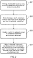
- FIG. 2 is a flowchart of a method according to an example.
- conductive traces are printed to a substrate using a thermoformable conductive ink, thereby forming a substrate/trace structure in a first topological configuration.
- a thermoforming process is executed in which the substrate/trace structure is heated and deformed. Although it may be possible to deform and then heat the structure, there is a risk of damage to the conductive traces before they have reached the temperature used for thermoforming, and so, in an example, the structure is heated to the first predetermined temperature before deformation.
- the structure, now deformed into a second topological configuration is allowed to cool to a second predetermined temperature whilst the deformation is maintained.
- the reduction from the first to the second predetermined temperature can be passive (i.e. simply allowing the structure to cool naturally), or active, in which some means is employed in order to more rapidly cool the structure, such as a fan or refrigeration and so on.
- thermoform only some portions of the conductive traces. That is, for example, heating and deformation (i.e. thermoforming) can be applied only in some sections of a substrate so that printed traces can will rendered stretch-resistant in only those sections where it is desired.
- conductive traces can be printed on sections of a substrate which will be subject to stretch when in use as well as sections that will not be subject to stretching during use.
- traces in the first section will be rendered stretch-resistant.
Landscapes
- Engineering & Computer Science (AREA)
- Microelectronics & Electronic Packaging (AREA)
- Chemical & Material Sciences (AREA)
- Life Sciences & Earth Sciences (AREA)
- Materials Engineering (AREA)
- Wood Science & Technology (AREA)
- Organic Chemistry (AREA)
- Manufacturing & Machinery (AREA)
- Laminated Bodies (AREA)
- Blow-Moulding Or Thermoforming Of Plastics Or The Like (AREA)
Abstract
Description
- Aspects relate to conductive traces, and methods for forming the same.
- Stretchable electronics and devices can be made by using the same components as used for rigid printed circuit boards, but can use a substrate and interconnections that can be stretched, compressed, and twisted for example. As such, they are capable of use in the field of wearables, smart garments and on-body/in-body electronics, and so on, as well as other applications in industrial and home Internet-of-things (IoT) devices.
- According to an example, there is provided a method of forming a conductive trace, the method comprising depositing a conductive trace material on a portion of an elastomeric substrate, a sub-portion of the elastomeric substrate comprising a first topological configuration, heating the sub-portion of the elastomeric substrate and conductive trace material deposited on that sub-portion to a first predetermined temperature, deforming the sub-portion of the elastomeric substrate and conductive trace material to a second topological configuration, and allowing the sub-portion of the elastomeric substrate and conductive trace material deposited on that sub-portion to cool to a second predetermined temperature whilst in the second topological configuration. The sub-portion can be deformed into the second topological configuration by applying a strain or force thereto. The method can further comprise releasing the strain applied on the sub-portion once it has cooled to the second predetermined temperature, thereby enabling the sub-portion of the substrate to revert to the first topological configuration. The first predetermined temperature can be selected from the range 30° C to 300° C; or 70° C to 150° C; or 90° C to 130° C. The sub-portion of the elastomeric substrate and conductive trace material can be actively cooled from the first predetermined temperature to the second predetermined temperature. The sub-portion of the elastomeric substrate can be deformed by stretching in one or more directions. The method can further comprise printing the conductive trace material onto the portion of an elastomeric substrate. The conductive trace material can be a thermoformable conductive ink. The conductive trace material deposited on the sub-portion can be thermoformed. Thermoforming the conductive trace can be performed by vacuum forming, pressure forming, drape forming, or stretch forming. The elastomeric substrate can be a rubber or thermoplastic elastomer.
- According to an example, there is provided a thermoformed conductive trace for use in a stretchable electronics apparatus formed on a substrate, the conductive trace applied to the substrate when the substrate is in an initial configuration and thermoformed when the substrate is in a second configuration. The trace can comprise an ink composition including conductive particles and a polymer resin. The conductive particles can be metallic or carbon-based particles, and the polymer resin can be composed of one or more of a vinyl, polyurethane or polyester resin. The conductive trace can have a softening temperature that is lower than a softening temperature of the elastomeric substrate.
- Embodiments will now be described, by way of example only, with reference to the accompanying drawings, in which:
-
Figure 1 is a schematic representation of an implementation of a method according to an example as applied to a substrate; and -
Figure 2 is a flowchart of a method according to an example. - Example embodiments are described below in sufficient detail to enable those of ordinary skill in the art to embody and implement the systems and processes herein described. It is important to understand that embodiments can be provided in many alternate forms and should not be construed as limited to the examples set forth herein.
- Accordingly, while embodiments can be modified in various ways and take on various alternative forms, specific embodiments thereof are shown in the drawings and described in detail below as examples. There is no intent to limit to the particular forms disclosed. On the contrary, all modifications, equivalents, and alternatives falling within the scope of the appended claims should be included. Elements of the example embodiments are consistently denoted by the same reference numerals throughout the drawings and detailed description where appropriate.
- The terminology used herein to describe embodiments is not intended to limit the scope. The articles "a," "an," and "the" are singular in that they have a single referent, however the use of the singular form in the present document should not preclude the presence of more than one referent. In other words, elements referred to in the singular can number one or more, unless the context clearly indicates otherwise. It will be further understood that the terms "comprises," "comprising," "includes," and/or "including," when used herein, specify the presence of stated features, items, steps, operations, elements, and/or components, but do not preclude the presence or addition of one or more other features, items, steps, operations, elements, components, and/or groups thereof.
- Unless otherwise defined, all terms (including technical and scientific terms) used herein are to be interpreted as is customary in the art. It will be further understood that terms in common usage should also be interpreted as is customary in the relevant art and not in an idealized or overly formal sense unless expressly so defined herein.
- In stretchable electronics, interconnections in the form of conductive traces for example, undergo large amounts of stress as the substrate onto (or into) which they are deposited changes shape. This can lead to changes in electrical resistance of the conductive traces when the substrate is subject to large stretching and can make them susceptible to hysteresis, that is their electrical resistance does not revert to the original value after multiple consecutive stretching (and relaxation) events.
- According to an example, there is provided a method of forming a conductive trace that improves the reliable performance of conductive traces. In an example, such conductive traces do not experience a change in electrical resistance upon large stretching of the substrate onto which they are deposited.
- In an example, conductive traces can comprise a thermoformable conductive ink. An Ink composition can comprise: 1) conductive particles including, for example, metal particles (e.g. silver, copper) or carbon-based particles (e.g. graphite, graphene, carbon nanotubes) or a blend of the two types; 2) a polymer resin such as, but not limited to, a vinyl resin, a polyurethane resin, a polyester resin, and combinations of these.
- The conductive ink can be deposited on an un-deformed (e.g. unstretched) substrate, such as an elastomeric substrate. In an example, such elastomers can include rubbers (e.g. ethylenepropylene-diene, neoprene, silicone rubbers, fluorosilicone rubbers, perfluoroelastomers) and thermoplastic elastomers (e.g. styrenics, polyurethanes, polyamides, polyolefin blends, polyolefin alloys, thermoplastic vulcanizates).
- The printed traces can then be thermoformed whilst the elastomeric substrate is deformed (e.g. stretched). In an example, it is possible that only a sub-portion of the substrate upon (or within) which the conductive trace is provided is deformed. The deformation can then be removed from the substrate, e.g. by release of strain, in order to enable it to revert to its initial configuration, thereby inducing a buckled geometry for the conductive traces.
- That is, according to an example, a conductive trace material can be deposited on a portion of an elastomeric substrate, a sub-portion of which is in a first topological configuration. In an example, the first topological configuration can be a relaxed or otherwise unstressed state of the substrate. The sub-portion of the elastomeric substrate and conductive trace material can then be heated to a first predetermined temperature. The first predetermined temperature can be selected as that at which the conductive trace can be thermoformed. For example, the first predetermined temperature can be selected from the range 30° C to 300° C; or 70° C to 150° C; or 90° C to 130° C.
- At the first predetermined temperature, the sub-portion of the elastomeric substrate and conductive trace material can be deformed to a second topological configuration, for example by stretching. The sub-portion of the substrate and conductive trace material can then be allowed to cool to a second predetermined temperature whilst in the second topological configuration. Once the sub-portion of the elastomeric substrate and conductive trace material have cooled to a second predetermined temperature, which is lower than the first predetermined temperature, the cause of the deformation can be removed, thereby resulting in the buckled conductive traces. In an example, the removal of the cause of deformation can be carried out at a subsequent point in time. For example, the cause of the deformation could be due to packaging (e.g. a t-shirt stretched over a cardboard cut-out), and thus the removal of the cause of the deformation may not occur until a consumer, for example, removes the product in question from the packaging, at which point the substrate may relax to the first topological configuration.
- Typically, thin films are transferred to a pre-stretched elastomeric substrate so that they will be buckled after the release of pre-strain. However, in examples of the present system, a thermoformable conductive ink is deposited or printed onto an un-stretched elastomeric substrate. In a second stage, the trace is thermoformed, i.e. stretched while heat is applied. Thus, the conductive trace is first permanently rendered longer during thermoforming and then compressed when the strain is released to create a buckled printed trace.
- Thermoformable inks were designed to be used on a substrate which permanently changes shape upon thermoforming. Thermoforming methods can include but are not limited to vacuum forming, pressure forming, drape forming, stretch forming.
However, in a method according to an example, thermoformable inks are used on an elastomeric substrate which does not permanently change shape during the thermoforming step. When the strain is released the elastomeric substrate goes back to its original size, whereas the thermoformed trace, which was permanently elongated, cannot go back to the original size and thus will be forced into taking a wavy shape, thus creating a buckled printed trace. - In an example, a softening temperature of a substrate can be higher than a softening temperature of a printed conductive trace. Accordingly, at a temperature high enough for the printed trace to become soft and be deformed without suffering structural damage, the substrate is still behaving as an elastomer and has not softened.
-
Figure 1 is a schematic representation of an implementation of a method according to an example as applied to a substrate. Asubstrate 100, such as an elastomeric substrate for example, is provided in a first topological configuration. In the example offigure 1 , thesubstrate 100 is in a first state in which it is at rest, i.e. not deformed. In an example, the first topological configuration of thesubstrate 100 can be such that it is in an initially or prestressed configuration. - Conductive traces 103 are deposited on the
substrate 100. For example, traces can be printed on a surface of thesubstrate 100 using a thermoformable conductive ink. Heat is applied to the substrate/trace combination to a first predetermined temperature, and the substrate is deformed into a secondtopological configuration 105. The heating and deformation process may be performed concurrently, or with one occurring before/after the other. As a result of the deformation of the substrate into theconfiguration 105, the conductive traces are also deformed 107. That is, since theconductive traces 103 are effectively adhered to thesubstrate 100, deformation of thesubstrate 100 results in a corresponding deformation of the conductive traces 103. Accordingly, in the example offigure 1 , the substrate and conductive traces are stretched. - The
deformed substrate 105 andconductive traces 107, having been thermoformed at the first predetermined temperature, are maintained in their deformed configuration as they are allowed to cool. Once cooled, removal of the cause of deformation will cause thesubstrate 105 to revert to its original size to providesubstrate 109. As a result of this, theconductive traces 107 buckle to form buckled traces 111. -
Figure 2 is a flowchart of a method according to an example. Inblock 201, conductive traces are printed to a substrate using a thermoformable conductive ink, thereby forming a substrate/trace structure in a first topological configuration. Inblock 203, a thermoforming process is executed in which the substrate/trace structure is heated and deformed. Although it may be possible to deform and then heat the structure, there is a risk of damage to the conductive traces before they have reached the temperature used for thermoforming, and so, in an example, the structure is heated to the first predetermined temperature before deformation. - In
block 205, the structure, now deformed into a second topological configuration, is allowed to cool to a second predetermined temperature whilst the deformation is maintained. The reduction from the first to the second predetermined temperature can be passive (i.e. simply allowing the structure to cool naturally), or active, in which some means is employed in order to more rapidly cool the structure, such as a fan or refrigeration and so on. - In
block 207, once the structure is at the second predetermined temperature, the deformation is released. The structure thus returns to the first topological configuration, and the conductive traces, which were permanently rendered longer, are forced to take on a buckled geometry that enables them to withstand repeated stretching events whilst maintaining constant or close-to-constant electrical resistance. - In an example, where the traces are deposited on large area substrates, it is possible to thermoform only some portions of the conductive traces. That is, for example, heating and deformation (i.e. thermoforming) can be applied only in some sections of a substrate so that printed traces can will rendered stretch-resistant in only those sections where it is desired.
- Accordingly, with a single deposition (e.g. printing) step, conductive traces can be printed on sections of a substrate which will be subject to stretch when in use as well as sections that will not be subject to stretching during use. In a subsequent thermoforming step, traces in the first section will be rendered stretch-resistant.
- The present inventions can be embodied in other specific apparatus and/or methods. The described embodiments are to be considered in all respects as illustrative and not restrictive. In particular, the scope of the invention is indicated by the appended claims rather than by the description and figures herein. All changes that come within the meaning and range of equivalency of the claims are to be embraced within their scope.
Claims (15)
- A method of forming a conductive trace, the method comprising:depositing a conductive trace material on a portion of an elastomeric substrate, a sub-portion of the elastomeric substrate comprising a first topological configuration;heating the sub-portion of the elastomeric substrate and conductive trace material deposited on that sub-portion to a first predetermined temperature;deforming the sub-portion of the elastomeric substrate and conductive trace material to a second topological configuration; andallowing the sub-portion of the elastomeric substrate and conductive trace material deposited on that sub-portion to cool to a second predetermined temperature whilst in the second topological configuration.
- The method as claimed in claim 1, wherein the sub-portion is deformed into the second topological configuration by applying a strain thereto.
- The method as claimed in claim 2, further comprising:releasing the strain applied on the sub-portion once it has cooled to the second predetermined temperature, thereby enabling the sub-portion of the elastomeric substrate to revert to the first topological configuration.
- The method as claimed in any preceding claim, wherein the first predetermined temperature is selected from the range 30° C to 300° C; or 70° C to 150° C; or 90° C to 130° C.
- The method as claimed in any preceding claim, wherein the sub-portion of the elastomeric substrate and conductive trace material are actively cooled from the first predetermined temperature to the second predetermined temperature.
- The method as claimed in any preceding claim, wherein the sub-portion of the elastomeric substrate is deformed by stretching in one or more directions.
- The method as claimed in any preceding claim, further comprising printing the conductive trace material onto the portion of an elastomeric substrate.
- The method as claimed in claim 7, wherein the conductive trace material is a thermoformable conductive ink.
- The method as claimed in any preceding claim, wherein the conductive trace material deposited on the sub-portion is thermoformed.
- The method as claimed in claim 9, wherein thermoforming the conductive trace is performed by vacuum forming, pressure forming, drape forming, or stretch forming.
- The method as claimed in any preceding claim, wherein the elastomeric substrate is a rubber or thermoplastic elastomer.
- A thermoformed conductive trace for use in a stretchable electronics apparatus formed on a substrate, the conductive trace applied to the substrate when the substrate is in an initial configuration and thermoformed when the substrate is in a second configuration.
- The thermoformed conductive trace as claimed in claim 12, wherein the trace comprises an ink composition including conductive particles and a polymer resin.
- The thermoformed conductive trace as claimed in claim 13, wherein the conductive particles are metallic or carbon-based particles, and the polymer resin is composed of one or more of a vinyl, polyurethane or polyester resin.
- The thermoformed conductive trace as claimed in any of claims 12 to 14, wherein the conductive trace has a softening temperature that is lower than a softening temperature of the substrate.
Priority Applications (2)
| Application Number | Priority Date | Filing Date | Title |
|---|---|---|---|
| EP18211577.4A EP3668282A1 (en) | 2018-12-11 | 2018-12-11 | Conductive traces |
| PCT/EP2019/084396 WO2020120461A1 (en) | 2018-12-11 | 2019-12-10 | Conductive traces |
Applications Claiming Priority (1)
| Application Number | Priority Date | Filing Date | Title |
|---|---|---|---|
| EP18211577.4A EP3668282A1 (en) | 2018-12-11 | 2018-12-11 | Conductive traces |
Publications (1)
| Publication Number | Publication Date |
|---|---|
| EP3668282A1 true EP3668282A1 (en) | 2020-06-17 |
Family
ID=64901297
Family Applications (1)
| Application Number | Title | Priority Date | Filing Date |
|---|---|---|---|
| EP18211577.4A Pending EP3668282A1 (en) | 2018-12-11 | 2018-12-11 | Conductive traces |
Country Status (2)
| Country | Link |
|---|---|
| EP (1) | EP3668282A1 (en) |
| WO (1) | WO2020120461A1 (en) |
Citations (3)
| Publication number | Priority date | Publication date | Assignee | Title |
|---|---|---|---|---|
| US20160170447A1 (en) * | 2014-12-10 | 2016-06-16 | Washington State University | Highly stretchable interconnect devices and systems |
| US20170347460A1 (en) * | 2016-05-27 | 2017-11-30 | Duke University | Stretchable Electrically Conductive Layer Formation By Aerosol Jet Printing On Flexible Substrate |
| WO2018146616A2 (en) * | 2017-02-08 | 2018-08-16 | National Research Council Of Canada | Printable molecular ink |
-
2018
- 2018-12-11 EP EP18211577.4A patent/EP3668282A1/en active Pending
-
2019
- 2019-12-10 WO PCT/EP2019/084396 patent/WO2020120461A1/en not_active Ceased
Patent Citations (3)
| Publication number | Priority date | Publication date | Assignee | Title |
|---|---|---|---|---|
| US20160170447A1 (en) * | 2014-12-10 | 2016-06-16 | Washington State University | Highly stretchable interconnect devices and systems |
| US20170347460A1 (en) * | 2016-05-27 | 2017-11-30 | Duke University | Stretchable Electrically Conductive Layer Formation By Aerosol Jet Printing On Flexible Substrate |
| WO2018146616A2 (en) * | 2017-02-08 | 2018-08-16 | National Research Council Of Canada | Printable molecular ink |
Non-Patent Citations (1)
| Title |
|---|
| JAEMYON LEE ET AL: "Paper;Lateral-crack-free, buckled, inkjet-printed silver electrodes on highly pre-stretched elastomeric substrates;Lateral-crack-free, buckled, inkjet-printed silver electrodes on highly pre-stretched elastomeric substrates", JOURNAL OF PHYSICS D: APPLIED PHYSICS, INSTITUTE OF PHYSICS PUBLISHING LTD, GB, vol. 46, no. 10, 12 February 2013 (2013-02-12), pages 105305, XP020241139, ISSN: 0022-3727, DOI: 10.1088/0022-3727/46/10/105305 * |
Also Published As
| Publication number | Publication date |
|---|---|
| WO2020120461A1 (en) | 2020-06-18 |
Similar Documents
| Publication | Publication Date | Title |
|---|---|---|
| JP7190453B2 (en) | elastic conductor | |
| KR101814375B1 (en) | Transparent conductive film | |
| CN106847688A (en) | A kind of stretchable electrode preparation method based on twin shaft pre-stretching | |
| US20220161517A1 (en) | Mechanical-metamaterial-based stretchable sustrate with negative poisson's ratio and manufacturing method thereof | |
| KR20160052352A (en) | Adhesive-type conductive buffer material | |
| EP3668282A1 (en) | Conductive traces | |
| US20220161462A1 (en) | Transparent stretchable substrate and manufacturing method thereof | |
| KR20140103515A (en) | Stamp structure for transfer printing and method of manufacturing the same, and transfer printing method using the stamp structure | |
| CN116156770B (en) | Flexible circuit board capable of repeatedly stretching and manufacturing method thereof | |
| CN103725214B (en) | Laminated body | |
| Ho et al. | Screen printing of stretchable electrodes for large area LED matrix | |
| US20240212876A1 (en) | Stretchable composite electrode and fabricating method thereof | |
| KR20140108829A (en) | Method for separating graphene thin film by roll to roll | |
| CN116168875B (en) | Liquid metal circuit and preparation method and application thereof | |
| JP2020002002A (en) | Tensile thin film structure and method of manufacturing the same | |
| KR101428926B1 (en) | Method of transferring a graphene thin layer | |
| US20150129283A1 (en) | Properties of printed conductive tracks | |
| US20160039191A1 (en) | Method for manufacturing composite material with fabric grain effect | |
| CN116867645B (en) | Membranes and their manufacturing methods, as well as methods for manufacturing semiconductor packages. | |
| WO2022200934A1 (en) | Haptic feedback device | |
| US20210178732A1 (en) | Electroactive polymers, methods of manufacture, and structures formed thereof | |
| JP7067902B2 (en) | Hydrophilization treatment method for thermoplastic sheet containing carbon material | |
| KR20170119974A (en) | Method for FORMING Flexible MULTI-LAYER Printed Circuit Board | |
| CN221848505U (en) | Automobile wire harness production control device | |
| KR20200080374A (en) | Method For Manufacturing Sheet Comprising Inherently Dissipative Polymer And Sheet Produced Therefrom |
Legal Events
| Date | Code | Title | Description |
|---|---|---|---|
| PUAI | Public reference made under article 153(3) epc to a published international application that has entered the european phase |
Free format text: ORIGINAL CODE: 0009012 |
|
| STAA | Information on the status of an ep patent application or granted ep patent |
Free format text: STATUS: THE APPLICATION HAS BEEN PUBLISHED |
|
| AK | Designated contracting states |
Kind code of ref document: A1 Designated state(s): AL AT BE BG CH CY CZ DE DK EE ES FI FR GB GR HR HU IE IS IT LI LT LU LV MC MK MT NL NO PL PT RO RS SE SI SK SM TR |
|
| AX | Request for extension of the european patent |
Extension state: BA ME |
|
| STAA | Information on the status of an ep patent application or granted ep patent |
Free format text: STATUS: REQUEST FOR EXAMINATION WAS MADE |
|
| 17P | Request for examination filed |
Effective date: 20201214 |
|
| RBV | Designated contracting states (corrected) |
Designated state(s): AL AT BE BG CH CY CZ DE DK EE ES FI FR GB GR HR HU IE IS IT LI LT LU LV MC MK MT NL NO PL PT RO RS SE SI SK SM TR |
|
| STAA | Information on the status of an ep patent application or granted ep patent |
Free format text: STATUS: EXAMINATION IS IN PROGRESS |
|
| 17Q | First examination report despatched |
Effective date: 20240223 |