EP3667269A1 - Light detector - Google Patents
Light detector Download PDFInfo
- Publication number
- EP3667269A1 EP3667269A1 EP18844873.2A EP18844873A EP3667269A1 EP 3667269 A1 EP3667269 A1 EP 3667269A1 EP 18844873 A EP18844873 A EP 18844873A EP 3667269 A1 EP3667269 A1 EP 3667269A1
- Authority
- EP
- European Patent Office
- Prior art keywords
- substrate
- main body
- wiring layer
- body portion
- layer
- Prior art date
- Legal status (The legal status is an assumption and is not a legal conclusion. Google has not performed a legal analysis and makes no representation as to the accuracy of the status listed.)
- Granted
Links
Images







Classifications
-
- G—PHYSICS
- G01—MEASURING; TESTING
- G01J—MEASUREMENT OF INTENSITY, VELOCITY, SPECTRAL CONTENT, POLARISATION, PHASE OR PULSE CHARACTERISTICS OF INFRARED, VISIBLE OR ULTRAVIOLET LIGHT; COLORIMETRY; RADIATION PYROMETRY
- G01J5/00—Radiation pyrometry, e.g. infrared or optical thermometry
- G01J5/10—Radiation pyrometry, e.g. infrared or optical thermometry using electric radiation detectors
- G01J5/20—Radiation pyrometry, e.g. infrared or optical thermometry using electric radiation detectors using resistors, thermistors or semiconductors sensitive to radiation, e.g. photoconductive devices
-
- G—PHYSICS
- G01—MEASURING; TESTING
- G01J—MEASUREMENT OF INTENSITY, VELOCITY, SPECTRAL CONTENT, POLARISATION, PHASE OR PULSE CHARACTERISTICS OF INFRARED, VISIBLE OR ULTRAVIOLET LIGHT; COLORIMETRY; RADIATION PYROMETRY
- G01J1/00—Photometry, e.g. photographic exposure meter
- G01J1/02—Details
-
- G—PHYSICS
- G01—MEASURING; TESTING
- G01J—MEASUREMENT OF INTENSITY, VELOCITY, SPECTRAL CONTENT, POLARISATION, PHASE OR PULSE CHARACTERISTICS OF INFRARED, VISIBLE OR ULTRAVIOLET LIGHT; COLORIMETRY; RADIATION PYROMETRY
- G01J5/00—Radiation pyrometry, e.g. infrared or optical thermometry
- G01J5/02—Constructional details
- G01J5/0225—Shape of the cavity itself or of elements contained in or suspended over the cavity
- G01J5/024—Special manufacturing steps or sacrificial layers or layer structures
-
- G—PHYSICS
- G01—MEASURING; TESTING
- G01J—MEASUREMENT OF INTENSITY, VELOCITY, SPECTRAL CONTENT, POLARISATION, PHASE OR PULSE CHARACTERISTICS OF INFRARED, VISIBLE OR ULTRAVIOLET LIGHT; COLORIMETRY; RADIATION PYROMETRY
- G01J5/00—Radiation pyrometry, e.g. infrared or optical thermometry
- G01J5/02—Constructional details
- G01J5/04—Casings
- G01J5/046—Materials; Selection of thermal materials
-
- H—ELECTRICITY
- H10—SEMICONDUCTOR DEVICES; ELECTRIC SOLID-STATE DEVICES NOT OTHERWISE PROVIDED FOR
- H10F—INORGANIC SEMICONDUCTOR DEVICES SENSITIVE TO INFRARED RADIATION, LIGHT, ELECTROMAGNETIC RADIATION OF SHORTER WAVELENGTH OR CORPUSCULAR RADIATION
- H10F30/00—Individual radiation-sensitive semiconductor devices in which radiation controls the flow of current through the devices, e.g. photodetectors
- H10F30/10—Individual radiation-sensitive semiconductor devices in which radiation controls the flow of current through the devices, e.g. photodetectors the devices being sensitive to infrared radiation, visible or ultraviolet radiation, and having no potential barriers, e.g. photoresistors
-
- H—ELECTRICITY
- H10—SEMICONDUCTOR DEVICES; ELECTRIC SOLID-STATE DEVICES NOT OTHERWISE PROVIDED FOR
- H10F—INORGANIC SEMICONDUCTOR DEVICES SENSITIVE TO INFRARED RADIATION, LIGHT, ELECTROMAGNETIC RADIATION OF SHORTER WAVELENGTH OR CORPUSCULAR RADIATION
- H10F39/00—Integrated devices, or assemblies of multiple devices, comprising at least one element covered by group H10F30/00, e.g. radiation detectors comprising photodiode arrays
- H10F39/10—Integrated devices
-
- H—ELECTRICITY
- H10—SEMICONDUCTOR DEVICES; ELECTRIC SOLID-STATE DEVICES NOT OTHERWISE PROVIDED FOR
- H10F—INORGANIC SEMICONDUCTOR DEVICES SENSITIVE TO INFRARED RADIATION, LIGHT, ELECTROMAGNETIC RADIATION OF SHORTER WAVELENGTH OR CORPUSCULAR RADIATION
- H10F39/00—Integrated devices, or assemblies of multiple devices, comprising at least one element covered by group H10F30/00, e.g. radiation detectors comprising photodiode arrays
- H10F39/10—Integrated devices
- H10F39/107—Integrated devices having multiple elements covered by H10F30/00 in a repetitive configuration, e.g. radiation detectors comprising photodiode arrays
-
- H—ELECTRICITY
- H10—SEMICONDUCTOR DEVICES; ELECTRIC SOLID-STATE DEVICES NOT OTHERWISE PROVIDED FOR
- H10F—INORGANIC SEMICONDUCTOR DEVICES SENSITIVE TO INFRARED RADIATION, LIGHT, ELECTROMAGNETIC RADIATION OF SHORTER WAVELENGTH OR CORPUSCULAR RADIATION
- H10F77/00—Constructional details of devices covered by this subclass
- H10F77/10—Semiconductor bodies
-
- H—ELECTRICITY
- H10—SEMICONDUCTOR DEVICES; ELECTRIC SOLID-STATE DEVICES NOT OTHERWISE PROVIDED FOR
- H10F—INORGANIC SEMICONDUCTOR DEVICES SENSITIVE TO INFRARED RADIATION, LIGHT, ELECTROMAGNETIC RADIATION OF SHORTER WAVELENGTH OR CORPUSCULAR RADIATION
- H10F77/00—Constructional details of devices covered by this subclass
- H10F77/40—Optical elements or arrangements
- H10F77/413—Optical elements or arrangements directly associated or integrated with the devices, e.g. back reflectors
Definitions
- the present disclosure relates to a light detector.
- a light detector there is known one including a substrate, a membrane disposed on a surface of the substrate so as to form a void space between the membrane and the surface of the substrate, and a pair of electrode posts supporting the membrane and the membrane includes a pair of wiring layers facing each other with a gap interposed therebetween and a resistance layer having an electrical resistance depending on a temperature.
- the electrode post has a cylindrical shape and the wiring layer is electrically connected to the electrode post in a connection portion of the electrode post in the membrane (for example, see Patent Literature 1).
- Patent Literature 1 US Unexamined Patent Publication No. 2011/42569
- an object of the present disclosure is to provide a light detector capable of suppressing an electrical connection error in a connection portion of the membrane, the connection portion to which the electrode post is connected.
- a light detector of an aspect of the present disclosure includes a substrate; a membrane which includes a light receiving portion, first and second connection portions, a first beam portion disposed between the light receiving portion and the first connection portion, and a second beam portion disposed between the light receiving portion and the second connection portion and is disposed on a surface of the substrate so that a void space is formed between the membrane and the surface of the substrate; a first electrode pad which is formed on the surface of the substrate; a second electrode pad which is formed on the surface of the substrate; a first electrode post which is disposed between the first electrode pad and the first connection portion so as to support the membrane and to electrically connect the membrane to the first electrode pad; and a second electrode post which is disposed between the second electrode pad and the second connection portion so as to support the membrane and to electrically connect the membrane to the second electrode pad, in which the membrane includes first and second wiring layers facing each other with a gap interposed therebetween in the light receiving portion and a resistance layer having an electrical resistance depending on a temperature and electrically connected to each of the first
- the first main body portion of the first electrode post has a tubular shape spreading from the first electrode pad toward the side opposite to the substrate. For this reason, stress concentration hardly occurs in the first connection portion of the membrane, the first connection portion to which the first electrode post is connected. The same applies to the second electrode post and stress concentration hardly occurs the second connection portion of the membrane, the second connection portion to which the second electrode post is connected. Further, the first flange portion is provided in an end portion at the side opposite to the substrate in the first main body portion of the first electrode post. For this reason, deformation hardly occurs in the first connection portion of the membrane, the first connection portion to which the first electrode post is connected.
- the second electrode post and deformation hardly occurs in the second connection portion of the membrane, the second connection portion to which the second electrode post is connected.
- the first wiring layer reaches the inner surface of the first main body portion through the first sloped surface provided in the first flange portion. For this reason, stress concentration hardly occurs in the first wiring layer itself at the first connection portion of the membrane, the first connection portion to which the first electrode post is connected.
- the second electrode post and stress concentration hardly occurs in the second wiring layer itself at the second connection portion of the membrane, the second connection portion to which the second electrode post is connected.
- the light detector it is possible to suppress an electrical connection error in the connection portion of the membrane, the connection portion to which the electrode post is connected.
- the first wiring layer may reach the inner surface of the first main body portion and an inner surface of the first bottom portion through the first sloped surface and the second wiring layer may reach the inner surface of the second main body portion and an inner surface of the second bottom portion through the second sloped surface. According to this configuration, it is possible to secure the electrical connection between the first wiring layer and the first electrode post and the electrical connection between the second wiring layer and the second electrode post.
- the first sloped surface may be provided in an annular shape along an outer edge of the first flange portion
- the first wiring layer may cover the first sloped surface and the inner surface of the first main body portion
- the second sloped surface may be provided in an annular shape along an outer edge of the second flange portion
- the second wiring layer may cover the second sloped surface and the inner surface of the second main body portion.
- the membrane may further include a first insulation layer formed on a surface at the side opposite to the substrate in the first wiring layer and the second wiring layer and the first insulation layer may cover a side surface of the first wiring layer in the first connection portion and cover a side surface of the second wiring layer in the second connection portion.
- the membrane may further include a second insulation layer formed on a surface at the side of the substrate in the first wiring layer and the second wiring layer and the second insulation layer may enter a groove formed in an outer surface of the first bottom portion on the first electrode pad through an outer surface of the first main body portion and enter a groove formed in an outer surface of the second bottom portion on the second electrode pad through an outer surface of the second main body portion.
- the resistance layer may be provided in the light receiving portion, the first connection portion, and the second connection portion and may be divided in each of the first beam portion and the second beam portion. According to this configuration, since the first connection portion and the second connection portion are reinforced by the resistance layer, it is possible to more reliably suppress an electrical connection error in the connection portion of the membrane, the connection portion to which the electrode post is connected. Further, since the resistance layer is divided in the first beam portion and the second beam portion, it is possible to suppress that heat generated in the light receiving portion escapes through the first beam portion and the second beam portion and to improve performance as the light detector.
- a light detector capable of suppressing an electrical connection error in a connection portion of a membrane, the connection portion to which an electrode post is connected.
- a light detector 1 illustrated in FIG. 1 detects light by using a function as a bolometer.
- the light is, for example, infrared rays including terahertz waves.
- the light detector 1 is used for an infrared imager, a thermography, or the like.
- the light detector 1 has excellent characteristics particularly for detecting light in a wavelength band of 1 ⁇ m to several tens of ⁇ m.
- the light detector 1 includes a substrate 2, a pixel unit 3, a reference unit 4, and a signal processing circuit unit 5.
- the substrate 2 is, for example, a Si substrate.
- the thickness of the substrate 2 is, for example, about several hundreds of ⁇ m.
- the pixel unit 3, the reference unit 4, and the signal processing circuit unit 5 are formed on the substrate 2.
- Each of the pixel unit 3 and the reference unit 4 is electrically connected to the signal processing circuit unit 5. Additionally, the signal processing circuit unit 5 may be formed within the substrate 2.
- the pixel unit 3 includes a plurality of light detecting elements 10.
- the plurality of light detecting elements 10 are arranged in a two-dimensional matrix shape.
- the light detecting element 10 includes the substrate 2 (precisely, a part of the substrate 2), a light reflection layer 61, a first electrode pad 62, a second electrode pad 63, a membrane 20, a first electrode post 7, and a second electrode post 8.
- the light reflection layer 61 is formed on a surface 2a of the substrate 2.
- the light reflection layer 61 faces a light absorption layer 36 to be described later in the thickness direction of the substrate 2 (that is, a direction perpendicular to the surface 2a of the substrate 2) and constitutes an optical resonance structure along with the light absorption layer 36.
- the thickness of the light reflection layer 61 is, for example, about several hundreds of nm.
- the material of the light reflection layer 61 is, for example, a metal material such as Al having high reflectivity with respect to light (for example, infrared rays).
- the first electrode pad 62 and the second electrode pad 63 are formed on the surface 2a of the substrate 2.
- the light reflection layer 61, the first electrode pad 62, and the second electrode pad 63 form, for example, a rectangular outer shape when viewed from the thickness direction of the substrate 2.
- the first electrode pad 62 and the second electrode pad 63 are located diagonally in the outer shape.
- Each of the first electrode pad 62 and the second electrode pad 63 has, for example, a rectangular shape when viewed from the thickness direction of the substrate 2.
- Each of the first electrode pad 62 and the second electrode pad 63 is electrically connected to the signal processing circuit unit 5 through a wiring (not illustrated) formed on the substrate 2.
- each of the first electrode pad 62 and the second electrode pad 63 is, for example, about several hundreds of nm.
- the material of each of the first electrode pad 62 and the second electrode pad 63 is, for example, a conductive metal material such as Al.
- the membrane 20 is disposed on the surface 2a of the substrate 2 so as to form a void space S between the membrane 20 and the surface 2a of the substrate 2.
- the membrane 20 is disposed in substantially parallel to the surface 2a of the substrate 2.
- a distance between the membrane 20 and the surface 2a of the substrate 2 is, for example, about several ⁇ m.
- the membrane 20 includes a light receiving portion 21, first and second connection portions 22 and 23, and first and second beam portions 24 and 25.
- the light receiving portion 21, the first and second connection portions 22 and 23, and the first and second beam portions 24 and 25 are integrally formed and form, for example, a rectangular outer shape when viewed from the thickness direction of the substrate 2.
- the first connection portion 22 and the second connection portion 23 are located diagonally in the outer shape.
- Each of the first connection portion 22 and the second connection portion 23 has, for example, a rectangular shape when viewed from the thickness direction of the substrate 2.
- the light receiving portion 21 faces the light reflection layer 61 in the thickness direction of the substrate 2.
- the first connection portion 22 faces the first electrode pad 62 in the thickness direction of the substrate 2.
- the second connection portion 23 faces the second electrode pad 63 in the thickness direction of the substrate 2.
- the first beam portion 24 is disposed between the light receiving portion 21 and the first connection portion 22.
- the first beam portion 24 extends along the outer edge of the light receiving portion 21 at one side of the light receiving portion 21.
- One end of the first beam portion 24 is connected to the first connection portion 22 and the other end of the first beam portion 24 is connected to the light receiving portion 21 at a position in the vicinity of the second connection portion 23.
- First slits 20a are continuously formed between the light receiving portion 21 and the first connection portion 22 and between the light receiving portion 21 and the first beam portion 24.
- the second beam portion 25 is disposed between the light receiving portion 21 and the second connection portion 23. The second beam portion 25 extends along the outer edge of the light receiving portion 21 at the other side of the light receiving portion 21.
- Second slits 20b are continuously formed between the light receiving portion 21 and the second connection portion 23 and between the light receiving portion 21 and the second beam portion 25.
- the width of each of the first beam portion 24 and the second beam portion 25 is, for example, about several ⁇ m.
- the length of each of the first beam portion 24 and the second beam portion 25 is, for example, about several tens to several hundreds of ⁇ m.
- the width of each of the first slit 20a and the second slit 20b is, for example, about several ⁇ m.
- the first electrode post 7 is disposed between the first electrode pad 62 and the first connection portion 22.
- the first electrode post 7 supports the membrane 20 and electrically connects the membrane 20 to the first electrode pad 62.
- the second electrode post 8 is disposed between the second electrode pad 63 and the second connection portion 23.
- the second electrode post 8 supports the membrane 20 and electrically connects the membrane 20 to the second electrode pad 63.
- the height of each of the first electrode post 7 and the second electrode post 8 is, for example, about several ⁇ m.
- the material of each of the first electrode post 7 and the second electrode post 8 is, for example, a metal material such as Ti.
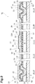
- FIG. 5 is a cross-sectional view of the light detecting element 10.
- I-I, II-II, III-III, IV-IV, and V-V of FIG. 5 are respectively cross-sectional views taken along lines I-I, II-II, III-III, IV-IV, and V-V of FIG. 4 .
- the membrane 20 includes first and second wiring layers 31 and 32, first and second insulation layers 33 and 34, a resistance layer 35, a light absorption layer 36, and a separation layer 37.
- the first wiring layer 31 and the second wiring layer 32 face each other through a gap G in the light receiving portion 21 when viewed from the thickness direction of the substrate 2.
- the gap G extends along the line L.
- the line L extends in a meandering shape so as to connect the first connection portion 22 and the second connection portion 23 when viewed from the thickness direction of the substrate 2.
- the line L includes a meandering portion L1.
- the meandering portion L1 includes a plurality of curved portions L2.
- the meandering portion L1 is formed in the light receiving portion 21 so as to repeat that extend to one side of the light receiving portion 21, turn back, for example, by 180° at the curved portion L2, extend to the other side of the light receiving portion 21, turn back, for example, by 180° at the curved portion L2, and extend to one side of the light receiving portion 21.
- one side means one side (for example, the existence side of the first beam portion 24) with respect to a line connecting the first connection portion 22 and the second connection portion 23 when viewed from the thickness direction of the substrate 2 and the other side means the side (for example, the existence side of the second beam portion 25) opposite to one side with respect to a line connecting the first connection portion 22 and the second connection portion 23 when viewed from the thickness direction of the substrate 2.
- one side means one side (for example, the existence side of the first beam portion 24) with respect to a line passing through the center of geometric of the membrane 20 when viewed from the thickness direction of the substrate 2 and the other side means the side (the existence side of the second beam portion 25) opposite to one side with respect to a line passing through the center of geometric of the membrane 20 when viewed from the thickness direction of the substrate 2.
- the length of each of the first wiring layer 31 and the second wiring layer 32 in a direction along the line L in the light receiving portion 21 when viewed from the thickness direction of the substrate 2 is, for example, about several tens to several hundreds of ⁇ m.
- the width of each of the first wiring layer 31 and the second wiring layer 32 in a direction perpendicular to the line L when viewed from the thickness direction of the substrate 2 is, for example, about several ⁇ m.
- the width of the gap G in a direction perpendicular to the line L when viewed from the thickness direction of the substrate 2 is, for example, about several ⁇ m.
- the direction perpendicular to the line L means a direction perpendicular to the tangent line at each position of the line L when viewed from the thickness direction of the substrate 2.
- the directions perpendicular to the line L are respectively different at respective positions of the curved portion.
- the thickness of each of the first wiring layer 31 and the second wiring layer 32 is, for example, about several tens to several hundreds of
- the first wiring layer 31 extends from the light receiving portion 21 to the first connection portion 22 through the first beam portion 24.
- the first wiring layer 31 is formed on the first electrode post 7 in the first connection portion 22.
- the first wiring layer 31 is electrically connected to the first electrode post 7.
- the second wiring layer 32 extends from the light receiving portion 21 to the second connection portion 23 through the second beam portion 25.
- the second wiring layer 32 is formed on the second electrode post 8 in the second connection portion 23.
- the second wiring layer 32 is electrically connected to the second electrode post 8.
- the material of each of the first wiring layer 31 and the second wiring layer 32 is, for example, a metal material such as Ti.
- the first insulation layer 33 is formed across the light receiving portion 21, the first and second beam portions 24 and 25, and the first and second connection portions 22 and 23 so as to cover the surface at the side opposite to the substrate 2 in each of the first wiring layer 31 and the second wiring layer 32.
- the first insulation layer 33 is formed in the surface at the side opposite to the substrate 2 in the first wiring layer 31 and the second wiring layer 32 while exposing an area along the line L in the surface at the side opposite to the substrate 2 in each of the first wiring layer 31 and the second wiring layer 32.
- the second insulation layer 34 is formed across the light receiving portion 21, the first and second beam portions 24 and 25, and the first and second connection portions 22 and 23 so as to cover the surface at the side of the substrate 2 in each of the first wiring layer 31 and the second wiring layer 32.
- each of the first insulation layer 33 and the second insulation layer 34 is, for example, about several tens of nm.
- the material of each of the first insulation layer 33 and the second insulation layer 34 is, for example, a silicon nitride film (SiN) or the like.
- the resistance layer 35 is formed so as to cover the first insulation layer 33 from the opposite side of the substrate 2 in the light receiving portion 21.
- the resistance layer 35 contacts an area along the line L in the surface opposite to the substrate 2 in each of the first wiring layer 31 and the second wiring layer 32 in the light receiving portion 21. That is, the resistance layer 35 is electrically connected to each of the first wiring layer 31 and the second wiring layer 32 in the light receiving portion 21.
- the resistance layer 35 has an electrical resistance that depends on temperature.
- the thickness of the resistance layer 35 is, for example, about several tens to several hundreds of nm.
- the material of the resistance layer 35 is, for example, amorphous silicon (a-Si) having a large change in electrical resistivity due to a temperature change.
- the light absorption layer 36 faces the surface 2a of the substrate 2 in the light receiving portion 21.
- the light absorption layer 36 is disposed at the side opposite to the substrate 2 with respect to the resistance layer 35.
- the light absorption layer 36 spreads over the entire area of the light receiving portion 21 when viewed from the thickness direction of the substrate 2.
- the thickness of the light absorption layer 36 is, for example, about a dozen of nm.
- the material of the light absorption layer 36 is, for example, WSi 2 or Ti.
- the separation layer 37 is formed across the light receiving portion 21, the first and second beam portions 24 and 25, and the first and second connection portions 22 and 23 so as to be located between the resistance layer 35 and the light absorption layer 36 in the light receiving portion 21.
- the thickness of the separation layer 37 is larger than the thickness of each of the first wiring layer 31, the second wiring layer 32, the resistance layer 35, and the light absorption layer 36.
- the thickness of the separation layer 37 is, for example, about several hundreds of nm.
- the material of the separation layer 37 is, for example, a silicon nitride film (SiN) or the like.
- the membrane 20 is provided with a plurality of through-holes 20c and 20d.
- the plurality of through-holes 20c and 20d are holes through which an etching gas for removing a sacrificial layer 69 to be described later passes.
- Each of the through-holes 20c and 20d has, for example, a circular shape when viewed from the thickness direction of the substrate 2.
- the diameter of each of the through-holes 20c and 20d is, for example, about several ⁇ m.
- configurations of the second electrode post 8 and the second connection portion 23 will be described in more detail with reference to FIG. 6 . Additionally, since the configurations of the first electrode post 7 and the first connection portion 22 are the same as the configurations of the second electrode post 8 and the second connection portion 23, the configurations of the first electrode post 7 and the first connection portion 22 are indicated by parentheses and the description thereof is omitted in FIG. 6 . I-I and V-V of FIG. 6 are respectively cross-sectional views taken along lines I-I and V-V of FIG. 4 .
- the second electrode post 8 includes a second main body portion 81, a second bottom portion 82, and a second flange portion 83.
- the second main body portion 81, the second bottom portion 82, and the second flange portion 83 are integrally formed by, for example, a metal material such as Ti.
- the second main body portion 81 is formed in, for example, a tubular shape such as a cylindrical shape spreading from the second electrode pad 63 toward the side opposite to the substrate 2.
- Each of the inner surface 81a and the outer surface 81b of the second main body portion 81 is, for example, a truncated cone-shaped tapered surface.
- the second bottom portion 82 is provided in an end portion at the side of the substrate 2 in the second main body portion 81.
- the second bottom portion 82 contacts the second electrode pad 63.
- An inner surface 82a of the second bottom portion 82 is, for example, a circular flat surface (a flat surface parallel to the surface 2a of the substrate 2) and is connected to the inner surface 81a of the second main body portion 81.
- the outer surface of the second bottom portion 82 is provided with a groove 82b extending in an annular shape along the outer edge of the outer surface of the second bottom portion 82.
- the groove 82b is defined by the second bottom portion 82 and the second electrode pad 63.
- the second flange portion 83 is provided in an end portion at the side opposite to the substrate 2 in the second main body portion 81.
- the second flange portion 83 is formed in a flange shape facing outward.
- a surface 83a at the side opposite to the substrate 2 in the second flange portion 83 is, for example, a flat surface (a flat surface parallel to the surface 2a of the substrate 2) having a circular inner edge and a rectangular outer edge and is connected to the inner surface 81a of the second main body portion 81.
- a surface 83b at the side of the substrate 2 in the second flange portion 83 is, for example, a flat surface (a flat surface parallel to the surface 2a of the substrate 2) having a circular inner edge and a rectangular outer edge and is connected to the outer surface 81b of the second main body portion 81.
- the outer edge of the surface 83a is connected to the outer edge of the surface 83b by the second sloped surface 83c. That is, the second sloped surface 83c is provided in an annular shape along the outer edge of the second flange portion 83.
- the second sloped surface 83c is inclined so as to approach the substrate 2 in a direction perpendicular to the surface 2a of the substrate 2 as it goes away from the second main body portion 81 in a direction parallel to the surface 2a of the substrate 2.
- the second sloped surface 83c is, for example, a square frustum tapered surface.
- the second wiring layer 32 extends to the second connection portion 23 through the second beam portion 25.
- the second wiring layer 32 reaches the inner surface 81a of the second main body portion 81 and the inner surface 82a of the second bottom portion 82 through the second sloped surface 83c and the surface 83a of the second flange portion 83 in the second connection portion 23.
- the second wiring layer 32 covers the second sloped surface 83c and the surface 83a of the second flange portion 83, the inner surface 81a of the second main body portion 81, and the inner surface 82a of the second bottom portion 82 in the second connection portion 23. Accordingly, the second wiring layer 32 is smoothly formed in the second connection portion 23 without being bent at a right angle or less.
- the first insulation layer 33 covers the side surface 32a of the second wiring layer 32 in the second connection portion 23.
- the second insulation layer 34 enters the groove 82b on the second electrode pad 63 through the surface at the side of the substrate 2 in the second wiring layer 32, the surface 83b of the second flange portion 83, and the outer surface 81b of the second main body portion 81. That is, in the second connection portion 23, a part of the second insulation layer 34 is disposed between the second electrode post 8 and the second electrode pad 63.
- the resistance layer 35 is also provided in the second connection portion 23 as well as the light receiving portion 21.
- the resistance layer 35 is not formed in a portion excluding both end portions of the second beam portion 25. That is, the resistance layer 35 is divided in the second beam portion 25.
- the configurations of the first electrode post 7 and the first connection portion 22 are respectively the same as the configurations of the second electrode post 8 and the second connection portion 23.
- the first electrode post 7 includes a first main body portion 71, a first bottom portion 72, and a first flange portion 73.
- the first main body portion 71, the first bottom portion 72, and the first flange portion 73 are integrally formed by, for example, a metal material such as Ti.
- the first main body portion 71 is formed in a tubular shape spreading from the first electrode pad 62 toward the side opposite to the substrate 2.
- the first bottom portion 72 is provided in an end portion at the side of the substrate 2 in the first main body portion 71.
- the first flange portion 73 is provided at an end portion at the side opposite to the substrate 2 in the first main body portion 71.
- the first flange portion 73 is provided with a first sloped surface 73c which is inclined so as to approach the substrate 2 as it goes away from the first main body portion 71.
- the first sloped surface 73c is provided in an annular shape along the outer edge of the first flange portion 73.
- the first wiring layer 31 extends to the first connection portion 22 through the first beam portion 24 and reaches an inner surface 71a of the first main body portion 71 and an inner surface 72a of the first bottom portion 72 through the first sloped surface 73c.
- the first wiring layer 31 covers the first sloped surface 73c, and the inner surface 71a of the first main body portion 71, and the inner surface 72a of the first bottom portion 72.
- the first insulation layer 33 covers the side surface 31a of the first wiring layer 31 in the first connection portion 22.
- the second insulation layer 34 enters a groove 72b formed on the outer surface of the first bottom portion 72 on the first electrode pad 62 through an outer surface 71b of the first main body portion 71.
- the resistance layer 35 is also provided in the first connection portion 22 as well as the light receiving portion 21.
- the resistance layer 35 is not formed in a portion excluding both end portions of the first beam portion 24. That is, the resistance layer 35 is divided in the first beam portion 24.
- the light detector 1 With the above-described configuration, light is detected as below.
- heat is generated in the light absorption layer 36 constituting an optical resonance structure to be described later.
- the light receiving portion 21 and the substrate 2 are thermally separated from one another by the void space S.
- the light receiving portion 21, the first connection portion 22, and the first beam portion 24 are thermally separated from one another by the first slit 20a.
- the light receiving portion 21, the second connection portion 23, and the second beam portion 25 are thermally separated from one another by the second slit 20b.
- the light absorption layer 36, the first wiring layer 31, and the second wiring layer 32 are thermally separated from one another by the separation layer 37. For this reason, it is possible to suppress that heat generated in the light absorption layer 36 escapes to the substrate 2 through the first wiring layer 31 and the second wiring layer 32 before the heat is sufficiently transmitted to the resistance layer 35 through the separation layer 37.
- Heat generated in the light absorption layer 36 is transmitted to the resistance layer 35 through the separation layer 37. Then, the temperature of the resistance layer 35 increases and the electrical resistance thereof decreases due to the heat.
- a change in electrical resistance is transmitted as a signal to the signal processing circuit unit 5 through the first and second wiring layers 31 and 32 and the first and second electrode posts 7 and 8.
- a change in electrical resistance of the resistance layer 35 is converted into a change in voltage or current.
- a change in electrical resistance is transmitted as a signal also from the reference element of the reference unit 4 to the signal processing circuit unit 5.
- a change in electrical resistance of the resistance layer of the reference element is converted into a change in voltage or current.
- the reference element is an element for compensating a change in temperature due to a factor other than the receiving of light in the light detecting element 10.
- light is detected on the basis of a difference between a change in voltage or current by the light detecting element 10 and a change in voltage or current by the reference element.
- a part of incident light A (having a wavelength ⁇ ) incident to the light absorption layer 36 is reflected by the light absorption layer 36 as reflected light B1 and the other is transmitted through the light absorption layer 36.
- Another part of the incident light A transmitted through the light absorption layer 36 is reflected by the light reflection layer 61 as reflected light B2.
- the reflected light B1 and the reflected light B2 are canceled by interference with each other on the reflecting surface of the light absorption layer 36. Accordingly, the incident light A is absorbed in the reflecting surface of the light absorption layer 36. Heat is generated in the light absorption layer 36 due to the energy of the absorbed incident light A.
- the absorption rate of the incident light A is determined by the sheet resistance of the light absorption layer 36 and the optical distance t between the light absorption layer 36 and the light reflection layer 61.
- the thickness of the light absorption layer 36 is set to about 16 nm so that the sheet resistance becomes a vacuum impedance (377 ⁇ /sq) (when the material of the light absorption layer 36 is WSi 2 ). Accordingly, the amplitude of the reflected light B1 reflected by the light absorption layer 36 matches the amplitude of the reflected light B2 reflected by the light reflection layer 61. For this reason, the reflected light B1 and the reflected light B2 are efficiently canceled by interference with each other on the reflecting surface of the light absorption layer 36. Thus, the absorption rate of the incident light A is improved.
- the light reflection layer 61 constitutes an optical resonance structure along with the light absorption layer 36. The incident light A is efficiently absorbed as the area of the overlapping portion between the light reflection layer 61 and the light absorption layer 36 becomes wider when viewed from the thickness direction of the substrate 2.
- the first main body portion 71 of the first electrode post 7 has a tubular shape spreading from the first electrode pad 62 toward the side opposite to the substrate 2. For this reason, stress concentration hardly occurs in the first connection portion 22 in the membrane 20. The same applies to the second electrode post 8 and stress concentration hardly occurs in the second connection portion 23. Further, the first main body portion 71 of the first electrode post 7 is provided with the first flange portion 73. For this reason, deformation hardly occurs in the first connection portion 22. The same applies to the second electrode post 8 and deformation hardly occurs in the second connection portion 23.
- the first wiring layer 31 reaches the inner surface 71a of the first main body portion 71 through the first sloped surface 73c provided in the first flange portion 73. For this reason, stress concentration hardly occurs in the first wiring layer 31 itself in the first connection portion 22. The same applies to the second electrode post 8 and stress concentration hardly occurs in the second wiring layer 32 itself in the second connection portion 23. Further, the first wiring layer 31 reaches not only the inner surface 71a of the first main body portion 71 but also the inner surface 72a of the first bottom portion 72 through the first sloped surface 73c. Accordingly, it is possible to secure the electrical connection between the first wiring layer 31 and the first electrode post 7. The same applies to the second electrode post 8 and the electrical connection between the second wiring layer 32 and the second electrode post 8 can be secured.
- the light detector 1 it is possible to suppress an electrical connection error in each of the first connection portion 22 and the second connection portion 23 respectively connected to the first electrode post 7 and the second electrode post 8 in the membrane 20. Further, according to the light detector 1, the thickness of the first electrode post 7 and the second electrode post 8 can be thickened and the thickness of the first wiring layer 31 and the second wiring layer 32 can be thinned. Accordingly, it is possible to reinforce the first electrode post 7 and the second electrode post 8 and to reduce the thermal conductance of the first wiring layer 31 and the second wiring layer 32 at the same time.
- the first sloped surface 73c is provided in an annular shape along the outer edge of the first flange portion 73
- the first wiring layer 31 covers the first sloped surface 73c and the inner surface 71a of the first main body portion 71
- the second sloped surface 83c is provided in an annular shape along the outer edge of the second flange portion 83
- the second wiring layer 32 covers the second sloped surface 83c and the inner surface 81a of the second main body portion 81.
- the first insulation layer 33 covers each of the side surface 31a of the first wiring layer 31 and the side surface 32a of the second wiring layer 32 in each of the first connection portion 22 and the second connection portion 23. According to this configuration, it is possible to prevent the separation of the first wiring layer 31 in the first connection portion 22 and the separation of the second wiring layer 32 in the second connection portion 23 while protecting the first wiring layer 31 and the second wiring layer 32 from the side opposite to the substrate 2.
- the second insulation layer 34 enters the groove 72b formed in the outer surface of the first bottom portion 72 on the first electrode pad 62 through the outer surface 71b of the first main body portion 71 of the first electrode post 7 in the first connection portion 22 and the second insulation layer 34 enters the groove 82b formed in the outer surface of the second bottom portion 82 on the second electrode pad 63 through the outer surface 81b of the second main body portion 81 of the second electrode post 8 in the second connection portion 23.
- the resistance layer 35 is provided in the light receiving portion 21, the first connection portion 22, and the second connection portion 23 and is divided in each of the first beam portion 24 and the second beam portion 25. According to this configuration, since the first connection portion 22 and the second connection portion 23 are reinforced by the resistance layer 35, it is possible to more reliably suppress an electrical connection error in each of the first connection portion 22 and the second connection portion 23 respectively connected to the first electrode post 7 and the second electrode post 8 in the membrane 20. Further, since the resistance layer 35 is divided in the first beam portion 24 and the second beam portion 25, it is possible to suppress that heat generated in the light receiving portion 21 escapes through the first beam portion 24 and the second beam portion 25 and to improve performance as the light detector 1.
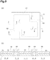
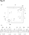
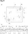
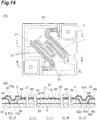
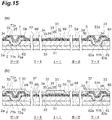
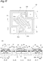
- FIGS. 8 to 17 I-I, II-II, III-III, IV-IV, and V-V of (b) are respectively cross-sectional views taken along lines I-I, II-II, III-III, IV-IV, and V-V of (a).
- FIGS. 15 and 16 the drawings as in (a) are omitted.
- the substrate 2 is prepared and the light reflection layer 61, the first electrode pad 62, and the second electrode pad 63 are formed on the surface 2a of the substrate 2.
- the light reflection layer 61, the first electrode pad 62, and the second electrode pad 63 are formed in the above-described shape by etching.
- the sacrificial layer 69 is formed on the surface 2a of the substrate 2 so as to cover the light reflection layer 61, the first electrode pad 62, and the second electrode pad 63.
- the material of the sacrificial layer 69 is, for example, polyimide or the like.
- a part of the sacrificial layer 69 is removed by etching so as to form through-holes 69a and 69b in the sacrificial layer 69.
- the through-holes 69a and 69b are respectively formed on the first electrode pad 62 and the second electrode pad 63. Then, in each of the through-holes 69a and 69b, the surface at the side opposite to the substrate 2 in each of the first electrode pad 62 and the second electrode pad 63 is exposed.
- Each of the inner surfaces of the through-holes 69a and 69b is, for example, a truncated cone-shaped tapered surface.
- Each of the inner surfaces of the through-holes 69a and 69b spreads from each of the first electrode pad 62 and the second electrode pad 63 toward the side opposite to the substrate 2.
- the second insulation layer 34 is formed on the sacrificial layer 69.
- the second insulation layer 34 is formed so that the inner surface of each of the through-holes 69a and 69b becomes, for example, a truncated cone-shaped tapered surface.
- a part of the second insulation layer 34 is removed by etching so as to form the through-holes 34a and 34b in the second insulation layer 34.
- the through-holes 34a and 34b are respectively formed on the first electrode pad 62 and the second electrode pad 63.
- the surface at the side opposite to the substrate 2 in each of the first electrode pad 62 and the second electrode pad 63 is exposed.
- Each of the through-holes 34a and 34b has a circular shape when viewed from the thickness direction of the substrate 2.
- the first electrode post 7 is formed on the second insulation layer 34 in the through-hole 69a and the second electrode post 8 is formed on the second insulation layer 34 in the through-hole 69b.
- Each of the first electrode post 7 and the second electrode post 8 is formed by, for example, vapor deposition.
- the inner surface of each of the through-holes 69a and 69b in the second insulation layer 34 is a tapered surface, each of the first electrode post 7 and the second electrode post 8 is more reliably formed. Accordingly, a disconnection due to poor film formation of the first electrode post 7 and the second electrode post 8 is suppressed. Thus, it is possible to suppress an electrical connection error in each of the first connection portion 22 and the second connection portion 23.
- each of the first electrode post 7 and the second electrode post 8 is suppressed and the strength is stabilized.
- the second insulation layer 34 includes a portion entering each of the groove 72b and the groove 82b in each of the first connection portion 22 and the second connection portion 23, the allowable range of misalignment between the first electrode post 7 and the second electrode post 8 is widened.
- the first wiring layer 31 and the second wiring layer 32 are formed on the second insulation layer 34 so as to cover the first electrode post 7 and the second electrode post 8.
- Each of the first wiring layer 31 and the second wiring layer 32 is formed by, for example, vapor deposition.
- the first sloped surface 73c of the first flange portion 73, the inner surface 71a of the first main body portion 71, the second sloped surface 83c of the second flange portion 83, and the inner surface 81a of the second main body portion 81 are tapered surfaces, the first wiring layer 31 and the second wiring layer 32 are more reliably formed on the first electrode post 7 and the second electrode post 8.
- the plurality of light detecting elements 10 are arranged in a two-dimensional matrix shape, an effect of more reliably forming the first and second electrode posts 7 and 8 and the first and second wiring layers 31 and 32 is particularly noticeable when the aspect ratio of the first electrode post 7 and the second electrode post 8 is increased in order to reduce a pixel pitch and a dead space.
- the first wiring layer 31 and the second wiring layer 32 are formed in the above-described shape by etching.
- the first insulation layer 33 is formed across the light receiving portion 21, the first and second beam portions 24 and 25, and the first and second connection portions 22 and 23 so as to cover the first wiring layer 31 and the second wiring layer 32 from the side opposite to the substrate 2.
- the first insulation layer 33 is formed in the above-described shape by etching.
- the first insulation layer 33 covers the side surface 31a of the first wiring layer 31 and the side surface 32a of the second wiring layer 32, the number of exposed dissimilar materials interfaces is small. Accordingly, etching defects caused by the interface can be reduced in the manufacturing process of the light detecting element 10. Further, since the type of material exposed to the outside is reduced, the degree of freedom in selecting an etching gas or an etching solution is improved.
- the resistance layer 35 is formed so as to cover the first insulation layer 33 from the side opposite to the substrate 2 in the light receiving portion 21 and the resistance layer 35 is formed on the first insulation layer 33 in the first connection portion 22 and the second connection portion 23.
- the separation layer 37 is formed so as to cover the resistance layer 35 from the side opposite to the substrate 2 in the light receiving portion 21, the first connection portion 22, and the second connection portion 23 and the separation layer 37 is formed on the first insulation layer 33 in the first beam portion 24 and the second beam portion 25.
- the light absorption layer 36 is formed on the separation layer 37 in the light receiving portion 21 and the through-holes 20c and 20d are further formed.
- the light absorption layer 36 is formed in the above-described shape by etching.
- the through-holes 20c and 20d are formed at the above-described positions by etching.
- the first slit 20a and the second slit 20b are formed and etching is further performed from the first slit 20a, the second slit 20b, and the through-holes 20c and 20d so as to remove the sacrificial layer 69 so that the void space S is formed.
- the first slit 20a and the second slit 20b are formed at the above-described positions by etching.
- the second wiring layer 32 may not reach the inner surface 82a of the second bottom portion 82.
- the second wiring layer 32 may reach the inner surface 81a of the second main body portion 81 through the second sloped surface 83c of the second flange portion 83 in the second connection portion 23.
- the same applies to the first wiring layer 31 and the first wiring layer 31 may not reach the inner surface 72a of the first bottom portion 72.
- the first wiring layer 31 may reach the inner surface 71a of the first main body portion 71 through the first sloped surface 73c of the first flange portion 73 in the first connection portion 22.
- the second sloped surface 83c may be provided, for example, only in a part of the outer edge of the second flange portion 83.
- the second wiring layer 32 may not cover the second sloped surface 83c, and the inner surface 81a of the second main body portion 81, and the inner surface 72a of the second bottom portion 82. The second wiring layer 32 may reach the inner surface 81a of the second main body portion 81 through the second sloped surface 83c.
- first electrode post 7 and the first sloped surface 73c may be provided, for example, only in a part of the outer edge of the first flange portion 73. Further, the first wiring layer 31 may not cover the first sloped surface 73c, and the inner surface 71a of the first main body portion 71, and the inner surface 72a of the first bottom portion 72. The first wiring layer 31 may reach the inner surface 71a of the first main body portion 71 through the first sloped surface 73c.
- each of the inner surface 81a and the outer surface 81b of the second main body portion 81 is a truncated cone-shaped tapered surface
- each of the inner surface 81a and the outer surface 81b of the second main body portion 81 may be, for example, a square frustum tapered surface.
- the same applies to the first main body portion 71 and each of the inner surface 71a and the outer surface 71b of the first main body portion 71 may be, for example, a square frustum tapered surface.
- each of the inner edge and the outer edge of the surface 83a may have, for example, a circular shape or a rectangular shape.
- each of the inner edge and the outer edge of the surface 83b at the side of the substrate 2 in the second flange portion 83 has a circular shape and the outer edge thereof has a rectangular shape
- each of the inner edge and the outer edge of the surface 83b may have, for example, a circular shape or a rectangular shape.
- each of the inner edge and the outer edge of the surface 73 a may have, for example, a circular shape or a rectangular shape.
- each of the inner edge and the outer edge of the surface 73b may have, for example, a circular shape or a rectangular shape.
- the membrane 20 has, for example, a rectangular shape when viewed from the thickness direction of the substrate 2 has been described, but the present disclosure is not limited thereto.
- the membrane 20 may have, for example, various shapes such as a circular shape when viewed from the thickness direction of the substrate 2.
- various materials and thicknesses can be selected for each of the first and second wiring layers 31 and 32, the resistance layer 35, the light absorption layer 36, and the separation layer 37. It is possible to easily improve the sensitivity and to improve the strength of the membrane 20 by selecting the optimum material and thickness for each of the first and second wiring layers 31 and 32, the resistance layer 35, and the separation layer 37. Further, it is possible to improve both sensitivity and response speed by selecting the optimum material for each of the first and second wiring layers 31 and 32 and the light absorption layer 36.
- the through-holes 20c and 20d may have various shapes such as an oval shape or a square shape when viewed from the thickness direction of the substrate 2. Further, the formation positions of the through-holes 20c and 20d are not limited. The through-holes 20c and 20d may be formed at various positions of the light receiving portion 21.
- the pixel unit 3 may be configured as one light detecting element 10.
Landscapes
- Physics & Mathematics (AREA)
- General Physics & Mathematics (AREA)
- Spectroscopy & Molecular Physics (AREA)
- Engineering & Computer Science (AREA)
- Manufacturing & Machinery (AREA)
- Photometry And Measurement Of Optical Pulse Characteristics (AREA)
- Solid State Image Pick-Up Elements (AREA)
Abstract
Description
- The present disclosure relates to a light detector.
- As a light detector, there is known one including a substrate, a membrane disposed on a surface of the substrate so as to form a void space between the membrane and the surface of the substrate, and a pair of electrode posts supporting the membrane and the membrane includes a pair of wiring layers facing each other with a gap interposed therebetween and a resistance layer having an electrical resistance depending on a temperature. In such a light detector, the electrode post has a cylindrical shape and the wiring layer is electrically connected to the electrode post in a connection portion of the electrode post in the membrane (for example, see Patent Literature 1).
- Patent Literature 1:
US Unexamined Patent Publication No. 2011/42569 - In the above-described light detector, since an outer surface of the electrode post intersects vertically a surface at the side of the substrate in the connection portion of the membrane, stress concentration easily occurs at the intersection portion. As a result, there is concern that an electrical connection error occurs in the connection portion of the membrane, the connection portion to which the electrode post is connected.
- Here, an object of the present disclosure is to provide a light detector capable of suppressing an electrical connection error in a connection portion of the membrane, the connection portion to which the electrode post is connected.
- A light detector of an aspect of the present disclosure includes a substrate; a membrane which includes a light receiving portion, first and second connection portions, a first beam portion disposed between the light receiving portion and the first connection portion, and a second beam portion disposed between the light receiving portion and the second connection portion and is disposed on a surface of the substrate so that a void space is formed between the membrane and the surface of the substrate; a first electrode pad which is formed on the surface of the substrate; a second electrode pad which is formed on the surface of the substrate; a first electrode post which is disposed between the first electrode pad and the first connection portion so as to support the membrane and to electrically connect the membrane to the first electrode pad; and a second electrode post which is disposed between the second electrode pad and the second connection portion so as to support the membrane and to electrically connect the membrane to the second electrode pad, in which the membrane includes first and second wiring layers facing each other with a gap interposed therebetween in the light receiving portion and a resistance layer having an electrical resistance depending on a temperature and electrically connected to each of the first and second wiring layers in the light receiving portion, in which the first electrode post includes a first main body portion having a tubular shape spreading from the first electrode pad toward the side opposite to the substrate, a first bottom portion provided in an end portion at the side of the substrate in the first main body portion, and a first flange portion provided in an end portion at the side opposite to the substrate in the first main body portion, in which the first flange portion is provided with a first sloped surface inclined so as to approach the substrate as it goes away from the first main body portion, in which the first wiring layer extends to the first connection portion through the first beam portion and reaches an inner surface of the first main body portion through the first sloped surface, in which the second electrode post includes a second main body portion having a tubular shape spreading from the second electrode pad toward the side opposite to the substrate, a second bottom portion provided in an end portion at the side of the substrate in the second main body portion, and a second flange portion provided in an end portion at the side opposite to the substrate in the second main body portion, in which the second flange portion is provided with a second sloped surface inclined so as to approach the substrate as it goes away from the second main body portion, and in which the second wiring layer extends to the second connection portion through the second beam portion and reaches an inner surface of the second main body portion through the second sloped surface.
- In the light detector, the first main body portion of the first electrode post has a tubular shape spreading from the first electrode pad toward the side opposite to the substrate. For this reason, stress concentration hardly occurs in the first connection portion of the membrane, the first connection portion to which the first electrode post is connected. The same applies to the second electrode post and stress concentration hardly occurs the second connection portion of the membrane, the second connection portion to which the second electrode post is connected. Further, the first flange portion is provided in an end portion at the side opposite to the substrate in the first main body portion of the first electrode post. For this reason, deformation hardly occurs in the first connection portion of the membrane, the first connection portion to which the first electrode post is connected. The same applies to the second electrode post and deformation hardly occurs in the second connection portion of the membrane, the second connection portion to which the second electrode post is connected. Further, the first wiring layer reaches the inner surface of the first main body portion through the first sloped surface provided in the first flange portion. For this reason, stress concentration hardly occurs in the first wiring layer itself at the first connection portion of the membrane, the first connection portion to which the first electrode post is connected. The same applies to the second electrode post and stress concentration hardly occurs in the second wiring layer itself at the second connection portion of the membrane, the second connection portion to which the second electrode post is connected. As described above, according to the light detector, it is possible to suppress an electrical connection error in the connection portion of the membrane, the connection portion to which the electrode post is connected.
- In the light detector of an aspect of the present disclosure, the first wiring layer may reach the inner surface of the first main body portion and an inner surface of the first bottom portion through the first sloped surface and the second wiring layer may reach the inner surface of the second main body portion and an inner surface of the second bottom portion through the second sloped surface. According to this configuration, it is possible to secure the electrical connection between the first wiring layer and the first electrode post and the electrical connection between the second wiring layer and the second electrode post.
- In the light detector of an aspect of the present disclosure, the first sloped surface may be provided in an annular shape along an outer edge of the first flange portion, the first wiring layer may cover the first sloped surface and the inner surface of the first main body portion, the second sloped surface may be provided in an annular shape along an outer edge of the second flange portion, and the second wiring layer may cover the second sloped surface and the inner surface of the second main body portion. According to this configuration, it is possible to further secure the electrical connection between the first wiring layer and the first electrode post and the electrical connection between the second wiring layer and the second electrode post.
- In the light detector of an aspect of the present disclosure, the membrane may further include a first insulation layer formed on a surface at the side opposite to the substrate in the first wiring layer and the second wiring layer and the first insulation layer may cover a side surface of the first wiring layer in the first connection portion and cover a side surface of the second wiring layer in the second connection portion. According to this configuration, it is possible to prevent the separation of the first wiring layer in the first connection portion and the separation of the second wiring layer in the second connection portion while protecting the first wiring layer and the second wiring layer from the side opposite to the substrate.
- In the light detector of an aspect of the present disclosure, the membrane may further include a second insulation layer formed on a surface at the side of the substrate in the first wiring layer and the second wiring layer and the second insulation layer may enter a groove formed in an outer surface of the first bottom portion on the first electrode pad through an outer surface of the first main body portion and enter a groove formed in an outer surface of the second bottom portion on the second electrode pad through an outer surface of the second main body portion. According to this configuration, it is possible to prevent the separation of the second insulation layer on the first electrode pad or the exposure of the outer surface of the first electrode post and the separation of the second insulation layer on the second electrode pad or the exposure of the outer surface of the second electrode post while protecting the first wiring layer and the second wiring layer from the substrate.
- In the light detector of an aspect of the present disclosure, the resistance layer may be provided in the light receiving portion, the first connection portion, and the second connection portion and may be divided in each of the first beam portion and the second beam portion. According to this configuration, since the first connection portion and the second connection portion are reinforced by the resistance layer, it is possible to more reliably suppress an electrical connection error in the connection portion of the membrane, the connection portion to which the electrode post is connected. Further, since the resistance layer is divided in the first beam portion and the second beam portion, it is possible to suppress that heat generated in the light receiving portion escapes through the first beam portion and the second beam portion and to improve performance as the light detector.
- According to the present disclosure, it is possible to provide a light detector capable of suppressing an electrical connection error in a connection portion of a membrane, the connection portion to which an electrode post is connected.
-
-
FIG. 1 is a plan view of a light detector of an embodiment. -
FIG. 2 is a plan view of a pixel unit of the light detector ofFIG. 1 . -
FIG. 3 is a perspective view of a light detecting element of the pixel unit ofFIG. 2 . -
FIG. 4 is a plan view of the light detecting element ofFIG. 3 . -
FIG. 5 is a cross-sectional view of the light detecting element ofFIG. 3 . -
FIG. 6 is a cross-sectional view of the light detecting element ofFIG. 3 . -
FIG. 7 is a diagram illustrating a principle of an optical resonance structure. -
FIG. 8 is a diagram illustrating a method of manufacturing the light detecting element ofFIG. 5 . -
FIG. 9 is a diagram illustrating a method of manufacturing the light detecting element ofFIG. 5 . -
FIG. 10 is a diagram illustrating a method of manufacturing the light detecting element ofFIG. 5 . -
FIG. 11 is a diagram illustrating a method of manufacturing the light detecting element ofFIG. 5 . -
FIG. 12 is a diagram illustrating a method of manufacturing the light detecting element ofFIG. 5 . -
FIG. 13 is a diagram illustrating a method of manufacturing the light detecting element ofFIG. 5 . -
FIG. 14 is a diagram illustrating a method of manufacturing the light detecting element ofFIG. 5 . -
FIG. 15 is a diagram illustrating a method of manufacturing the light detecting element ofFIG. 5 . -
FIG. 16 is a diagram illustrating a method of manufacturing the light detecting element ofFIG 5 . -
FIG. 17 is a diagram illustrating a method of manufacturing the light detecting element ofFIG. 5 . - Hereinafter, a preferred embodiment of the present disclosure will be described in detail with reference to the drawings. Additionally, the same reference numerals will be given to the same or equivalent parts in the drawings and a redundant description thereof will be omitted.
- A
light detector 1 illustrated inFIG. 1 detects light by using a function as a bolometer. The light is, for example, infrared rays including terahertz waves. When the light is infrared rays, thelight detector 1 is used for an infrared imager, a thermography, or the like. Thelight detector 1 has excellent characteristics particularly for detecting light in a wavelength band of 1 µm to several tens of µm. As illustrated inFIG. 1 , thelight detector 1 includes asubstrate 2, apixel unit 3, areference unit 4, and a signalprocessing circuit unit 5. Thesubstrate 2 is, for example, a Si substrate. The thickness of thesubstrate 2 is, for example, about several hundreds of µm. Thepixel unit 3, thereference unit 4, and the signalprocessing circuit unit 5 are formed on thesubstrate 2. Each of thepixel unit 3 and thereference unit 4 is electrically connected to the signalprocessing circuit unit 5. Additionally, the signalprocessing circuit unit 5 may be formed within thesubstrate 2. - As illustrated in
FIG. 2 , thepixel unit 3 includes a plurality of light detectingelements 10. The plurality of light detectingelements 10 are arranged in a two-dimensional matrix shape. As illustrated inFIG. 3 , thelight detecting element 10 includes the substrate 2 (precisely, a part of the substrate 2), alight reflection layer 61, afirst electrode pad 62, asecond electrode pad 63, amembrane 20, afirst electrode post 7, and asecond electrode post 8. - The
light reflection layer 61 is formed on asurface 2a of thesubstrate 2. Thelight reflection layer 61 faces alight absorption layer 36 to be described later in the thickness direction of the substrate 2 (that is, a direction perpendicular to thesurface 2a of the substrate 2) and constitutes an optical resonance structure along with thelight absorption layer 36. The thickness of thelight reflection layer 61 is, for example, about several hundreds of nm. The material of thelight reflection layer 61 is, for example, a metal material such as Al having high reflectivity with respect to light (for example, infrared rays). - The
first electrode pad 62 and thesecond electrode pad 63 are formed on thesurface 2a of thesubstrate 2. Thelight reflection layer 61, thefirst electrode pad 62, and thesecond electrode pad 63 form, for example, a rectangular outer shape when viewed from the thickness direction of thesubstrate 2. Thefirst electrode pad 62 and thesecond electrode pad 63 are located diagonally in the outer shape. Each of thefirst electrode pad 62 and thesecond electrode pad 63 has, for example, a rectangular shape when viewed from the thickness direction of thesubstrate 2. Each of thefirst electrode pad 62 and thesecond electrode pad 63 is electrically connected to the signalprocessing circuit unit 5 through a wiring (not illustrated) formed on thesubstrate 2. The thickness of each of thefirst electrode pad 62 and thesecond electrode pad 63 is, for example, about several hundreds of nm. The material of each of thefirst electrode pad 62 and thesecond electrode pad 63 is, for example, a conductive metal material such as Al. - The
membrane 20 is disposed on thesurface 2a of thesubstrate 2 so as to form a void space S between themembrane 20 and thesurface 2a of thesubstrate 2. Themembrane 20 is disposed in substantially parallel to thesurface 2a of thesubstrate 2. A distance between themembrane 20 and thesurface 2a of thesubstrate 2 is, for example, about several µm. As illustrated inFIGS. 3 and4 , themembrane 20 includes alight receiving portion 21, first andsecond connection portions second beam portions light receiving portion 21, the first andsecond connection portions second beam portions substrate 2. Thefirst connection portion 22 and thesecond connection portion 23 are located diagonally in the outer shape. Each of thefirst connection portion 22 and thesecond connection portion 23 has, for example, a rectangular shape when viewed from the thickness direction of thesubstrate 2. - The
light receiving portion 21 faces thelight reflection layer 61 in the thickness direction of thesubstrate 2. Thefirst connection portion 22 faces thefirst electrode pad 62 in the thickness direction of thesubstrate 2. Thesecond connection portion 23 faces thesecond electrode pad 63 in the thickness direction of thesubstrate 2. - The
first beam portion 24 is disposed between the light receivingportion 21 and thefirst connection portion 22. Thefirst beam portion 24 extends along the outer edge of thelight receiving portion 21 at one side of thelight receiving portion 21. One end of thefirst beam portion 24 is connected to thefirst connection portion 22 and the other end of thefirst beam portion 24 is connected to thelight receiving portion 21 at a position in the vicinity of thesecond connection portion 23.First slits 20a are continuously formed between the light receivingportion 21 and thefirst connection portion 22 and between the light receivingportion 21 and thefirst beam portion 24. Thesecond beam portion 25 is disposed between the light receivingportion 21 and thesecond connection portion 23. Thesecond beam portion 25 extends along the outer edge of thelight receiving portion 21 at the other side of thelight receiving portion 21. One end of thesecond beam portion 25 is connected to thesecond connection portion 23 and the other end of thesecond beam portion 25 is connected to thelight receiving portion 21 at a position in the vicinity of thefirst connection portion 22.Second slits 20b are continuously formed between the light receivingportion 21 and thesecond connection portion 23 and between the light receivingportion 21 and thesecond beam portion 25. The width of each of thefirst beam portion 24 and thesecond beam portion 25 is, for example, about several µm. The length of each of thefirst beam portion 24 and thesecond beam portion 25 is, for example, about several tens to several hundreds of µm. The width of each of thefirst slit 20a and thesecond slit 20b is, for example, about several µm. - The
first electrode post 7 is disposed between thefirst electrode pad 62 and thefirst connection portion 22. Thefirst electrode post 7 supports themembrane 20 and electrically connects themembrane 20 to thefirst electrode pad 62. Thesecond electrode post 8 is disposed between thesecond electrode pad 63 and thesecond connection portion 23. Thesecond electrode post 8 supports themembrane 20 and electrically connects themembrane 20 to thesecond electrode pad 63. The height of each of thefirst electrode post 7 and thesecond electrode post 8 is, for example, about several µm. The material of each of thefirst electrode post 7 and thesecond electrode post 8 is, for example, a metal material such as Ti. -
FIG. 5 is a cross-sectional view of thelight detecting element 10. I-I, II-II, III-III, IV-IV, and V-V ofFIG. 5 are respectively cross-sectional views taken along lines I-I, II-II, III-III, IV-IV, and V-V ofFIG. 4 . As illustrated inFIG. 5 , themembrane 20 includes first and second wiring layers 31 and 32, first and second insulation layers 33 and 34, aresistance layer 35, alight absorption layer 36, and aseparation layer 37. - As illustrated in
FIGS. 4 and5 , thefirst wiring layer 31 and thesecond wiring layer 32 face each other through a gap G in thelight receiving portion 21 when viewed from the thickness direction of thesubstrate 2. The gap G extends along the line L. For example, the line L extends in a meandering shape so as to connect thefirst connection portion 22 and thesecond connection portion 23 when viewed from the thickness direction of thesubstrate 2. Specifically, the line L includes a meandering portion L1. The meandering portion L1 includes a plurality of curved portions L2. The meandering portion L1 is formed in thelight receiving portion 21 so as to repeat that extend to one side of thelight receiving portion 21, turn back, for example, by 180° at the curved portion L2, extend to the other side of thelight receiving portion 21, turn back, for example, by 180° at the curved portion L2, and extend to one side of thelight receiving portion 21. - In this embodiment, one side means one side (for example, the existence side of the first beam portion 24) with respect to a line connecting the
first connection portion 22 and thesecond connection portion 23 when viewed from the thickness direction of thesubstrate 2 and the other side means the side (for example, the existence side of the second beam portion 25) opposite to one side with respect to a line connecting thefirst connection portion 22 and thesecond connection portion 23 when viewed from the thickness direction of thesubstrate 2. Further, one side means one side (for example, the existence side of the first beam portion 24) with respect to a line passing through the center of geometric of themembrane 20 when viewed from the thickness direction of thesubstrate 2 and the other side means the side (the existence side of the second beam portion 25) opposite to one side with respect to a line passing through the center of geometric of themembrane 20 when viewed from the thickness direction of thesubstrate 2. - The length of each of the
first wiring layer 31 and thesecond wiring layer 32 in a direction along the line L in thelight receiving portion 21 when viewed from the thickness direction of thesubstrate 2 is, for example, about several tens to several hundreds of µm. The width of each of thefirst wiring layer 31 and thesecond wiring layer 32 in a direction perpendicular to the line L when viewed from the thickness direction of thesubstrate 2 is, for example, about several µm. The width of the gap G in a direction perpendicular to the line L when viewed from the thickness direction of thesubstrate 2 is, for example, about several µm. The direction perpendicular to the line L means a direction perpendicular to the tangent line at each position of the line L when viewed from the thickness direction of thesubstrate 2. The directions perpendicular to the line L are respectively different at respective positions of the curved portion. The thickness of each of thefirst wiring layer 31 and thesecond wiring layer 32 is, for example, about several tens to several hundreds of nm. - The
first wiring layer 31 extends from thelight receiving portion 21 to thefirst connection portion 22 through thefirst beam portion 24. Thefirst wiring layer 31 is formed on thefirst electrode post 7 in thefirst connection portion 22. Thefirst wiring layer 31 is electrically connected to thefirst electrode post 7. Thesecond wiring layer 32 extends from thelight receiving portion 21 to thesecond connection portion 23 through thesecond beam portion 25. Thesecond wiring layer 32 is formed on thesecond electrode post 8 in thesecond connection portion 23. Thesecond wiring layer 32 is electrically connected to thesecond electrode post 8. The material of each of thefirst wiring layer 31 and thesecond wiring layer 32 is, for example, a metal material such as Ti. - The
first insulation layer 33 is formed across thelight receiving portion 21, the first andsecond beam portions second connection portions substrate 2 in each of thefirst wiring layer 31 and thesecond wiring layer 32. Thefirst insulation layer 33 is formed in the surface at the side opposite to thesubstrate 2 in thefirst wiring layer 31 and thesecond wiring layer 32 while exposing an area along the line L in the surface at the side opposite to thesubstrate 2 in each of thefirst wiring layer 31 and thesecond wiring layer 32. Thesecond insulation layer 34 is formed across thelight receiving portion 21, the first andsecond beam portions second connection portions substrate 2 in each of thefirst wiring layer 31 and thesecond wiring layer 32. The thickness of each of thefirst insulation layer 33 and thesecond insulation layer 34 is, for example, about several tens of nm. The material of each of thefirst insulation layer 33 and thesecond insulation layer 34 is, for example, a silicon nitride film (SiN) or the like. - The
resistance layer 35 is formed so as to cover thefirst insulation layer 33 from the opposite side of thesubstrate 2 in thelight receiving portion 21. Theresistance layer 35 contacts an area along the line L in the surface opposite to thesubstrate 2 in each of thefirst wiring layer 31 and thesecond wiring layer 32 in thelight receiving portion 21. That is, theresistance layer 35 is electrically connected to each of thefirst wiring layer 31 and thesecond wiring layer 32 in thelight receiving portion 21. Theresistance layer 35 has an electrical resistance that depends on temperature. The thickness of theresistance layer 35 is, for example, about several tens to several hundreds of nm. The material of theresistance layer 35 is, for example, amorphous silicon (a-Si) having a large change in electrical resistivity due to a temperature change. - The
light absorption layer 36 faces thesurface 2a of thesubstrate 2 in thelight receiving portion 21. Thelight absorption layer 36 is disposed at the side opposite to thesubstrate 2 with respect to theresistance layer 35. Thelight absorption layer 36 spreads over the entire area of thelight receiving portion 21 when viewed from the thickness direction of thesubstrate 2. The thickness of thelight absorption layer 36 is, for example, about a dozen of nm. The material of thelight absorption layer 36 is, for example, WSi2 or Ti. - The
separation layer 37 is formed across thelight receiving portion 21, the first andsecond beam portions second connection portions resistance layer 35 and thelight absorption layer 36 in thelight receiving portion 21. The thickness of theseparation layer 37 is larger than the thickness of each of thefirst wiring layer 31, thesecond wiring layer 32, theresistance layer 35, and thelight absorption layer 36. The thickness of theseparation layer 37 is, for example, about several hundreds of nm. The material of theseparation layer 37 is, for example, a silicon nitride film (SiN) or the like. - The
membrane 20 is provided with a plurality of through-holes holes sacrificial layer 69 to be described later passes. Each of the through-holes substrate 2. The diameter of each of the through-holes - Next, configurations of the
second electrode post 8 and thesecond connection portion 23 will be described in more detail with reference toFIG. 6 . Additionally, since the configurations of thefirst electrode post 7 and thefirst connection portion 22 are the same as the configurations of thesecond electrode post 8 and thesecond connection portion 23, the configurations of thefirst electrode post 7 and thefirst connection portion 22 are indicated by parentheses and the description thereof is omitted inFIG. 6 . I-I and V-V ofFIG. 6 are respectively cross-sectional views taken along lines I-I and V-V ofFIG. 4 . - As illustrated in
FIG. 6 , thesecond electrode post 8 includes a secondmain body portion 81, asecond bottom portion 82, and asecond flange portion 83. The secondmain body portion 81, thesecond bottom portion 82, and thesecond flange portion 83 are integrally formed by, for example, a metal material such as Ti. The secondmain body portion 81 is formed in, for example, a tubular shape such as a cylindrical shape spreading from thesecond electrode pad 63 toward the side opposite to thesubstrate 2. Each of theinner surface 81a and theouter surface 81b of the secondmain body portion 81 is, for example, a truncated cone-shaped tapered surface. - The
second bottom portion 82 is provided in an end portion at the side of thesubstrate 2 in the secondmain body portion 81. Thesecond bottom portion 82 contacts thesecond electrode pad 63. Aninner surface 82a of thesecond bottom portion 82 is, for example, a circular flat surface (a flat surface parallel to thesurface 2a of the substrate 2) and is connected to theinner surface 81a of the secondmain body portion 81. The outer surface of thesecond bottom portion 82 is provided with agroove 82b extending in an annular shape along the outer edge of the outer surface of thesecond bottom portion 82. Thegroove 82b is defined by thesecond bottom portion 82 and thesecond electrode pad 63. - The
second flange portion 83 is provided in an end portion at the side opposite to thesubstrate 2 in the secondmain body portion 81. Thesecond flange portion 83 is formed in a flange shape facing outward. Asurface 83a at the side opposite to thesubstrate 2 in thesecond flange portion 83 is, for example, a flat surface (a flat surface parallel to thesurface 2a of the substrate 2) having a circular inner edge and a rectangular outer edge and is connected to theinner surface 81a of the secondmain body portion 81. Asurface 83b at the side of thesubstrate 2 in thesecond flange portion 83 is, for example, a flat surface (a flat surface parallel to thesurface 2a of the substrate 2) having a circular inner edge and a rectangular outer edge and is connected to theouter surface 81b of the secondmain body portion 81. In thesecond flange portion 83, the outer edge of thesurface 83a is connected to the outer edge of thesurface 83b by the second slopedsurface 83c. That is, the second slopedsurface 83c is provided in an annular shape along the outer edge of thesecond flange portion 83. The secondsloped surface 83c is inclined so as to approach thesubstrate 2 in a direction perpendicular to thesurface 2a of thesubstrate 2 as it goes away from the secondmain body portion 81 in a direction parallel to thesurface 2a of thesubstrate 2. The secondsloped surface 83c is, for example, a square frustum tapered surface. - The
second wiring layer 32 extends to thesecond connection portion 23 through thesecond beam portion 25. Thesecond wiring layer 32 reaches theinner surface 81a of the secondmain body portion 81 and theinner surface 82a of thesecond bottom portion 82 through the second slopedsurface 83c and thesurface 83a of thesecond flange portion 83 in thesecond connection portion 23. Thesecond wiring layer 32 covers the second slopedsurface 83c and thesurface 83a of thesecond flange portion 83, theinner surface 81a of the secondmain body portion 81, and theinner surface 82a of thesecond bottom portion 82 in thesecond connection portion 23. Accordingly, thesecond wiring layer 32 is smoothly formed in thesecond connection portion 23 without being bent at a right angle or less. - The
first insulation layer 33 covers theside surface 32a of thesecond wiring layer 32 in thesecond connection portion 23. In thesecond connection portion 23, thesecond insulation layer 34 enters thegroove 82b on thesecond electrode pad 63 through the surface at the side of thesubstrate 2 in thesecond wiring layer 32, thesurface 83b of thesecond flange portion 83, and theouter surface 81b of the secondmain body portion 81. That is, in thesecond connection portion 23, a part of thesecond insulation layer 34 is disposed between thesecond electrode post 8 and thesecond electrode pad 63. Theresistance layer 35 is also provided in thesecond connection portion 23 as well as thelight receiving portion 21. Theresistance layer 35 is not formed in a portion excluding both end portions of thesecond beam portion 25. That is, theresistance layer 35 is divided in thesecond beam portion 25. - The configurations of the
first electrode post 7 and thefirst connection portion 22 are respectively the same as the configurations of thesecond electrode post 8 and thesecond connection portion 23. Here, not thesecond wiring layer 32 but thefirst wiring layer 31 extends in thefirst connection portion 22. That is, thefirst electrode post 7 includes a firstmain body portion 71, afirst bottom portion 72, and afirst flange portion 73. The firstmain body portion 71, thefirst bottom portion 72, and thefirst flange portion 73 are integrally formed by, for example, a metal material such as Ti. The firstmain body portion 71 is formed in a tubular shape spreading from thefirst electrode pad 62 toward the side opposite to thesubstrate 2. Thefirst bottom portion 72 is provided in an end portion at the side of thesubstrate 2 in the firstmain body portion 71. Thefirst flange portion 73 is provided at an end portion at the side opposite to thesubstrate 2 in the firstmain body portion 71. Thefirst flange portion 73 is provided with a first slopedsurface 73c which is inclined so as to approach thesubstrate 2 as it goes away from the firstmain body portion 71. The firstsloped surface 73c is provided in an annular shape along the outer edge of thefirst flange portion 73. Thefirst wiring layer 31 extends to thefirst connection portion 22 through thefirst beam portion 24 and reaches aninner surface 71a of the firstmain body portion 71 and aninner surface 72a of thefirst bottom portion 72 through the first slopedsurface 73c. Thefirst wiring layer 31 covers the first slopedsurface 73c, and theinner surface 71a of the firstmain body portion 71, and theinner surface 72a of thefirst bottom portion 72. Thefirst insulation layer 33 covers theside surface 31a of thefirst wiring layer 31 in thefirst connection portion 22. Thesecond insulation layer 34 enters agroove 72b formed on the outer surface of thefirst bottom portion 72 on thefirst electrode pad 62 through anouter surface 71b of the firstmain body portion 71. Theresistance layer 35 is also provided in thefirst connection portion 22 as well as thelight receiving portion 21. Theresistance layer 35 is not formed in a portion excluding both end portions of thefirst beam portion 24. That is, theresistance layer 35 is divided in thefirst beam portion 24. - In the
light detector 1 with the above-described configuration, light is detected as below. First, when light is incident to thelight receiving portion 21, heat is generated in thelight absorption layer 36 constituting an optical resonance structure to be described later. At this time, thelight receiving portion 21 and thesubstrate 2 are thermally separated from one another by the void space S. Further, thelight receiving portion 21, thefirst connection portion 22, and thefirst beam portion 24 are thermally separated from one another by thefirst slit 20a. Further, thelight receiving portion 21, thesecond connection portion 23, and thesecond beam portion 25 are thermally separated from one another by thesecond slit 20b. For this reason, it is possible to suppress that heat generated in thelight absorption layer 36 escapes to thesubstrate 2 through thefirst beam portion 24, thefirst connection portion 22, thesecond beam portion 25, and thesecond connection portion 23. Further, thelight absorption layer 36, thefirst wiring layer 31, and thesecond wiring layer 32 are thermally separated from one another by theseparation layer 37. For this reason, it is possible to suppress that heat generated in thelight absorption layer 36 escapes to thesubstrate 2 through thefirst wiring layer 31 and thesecond wiring layer 32 before the heat is sufficiently transmitted to theresistance layer 35 through theseparation layer 37. - Heat generated in the
light absorption layer 36 is transmitted to theresistance layer 35 through theseparation layer 37. Then, the temperature of theresistance layer 35 increases and the electrical resistance thereof decreases due to the heat. A change in electrical resistance is transmitted as a signal to the signalprocessing circuit unit 5 through the first and second wiring layers 31 and 32 and the first andsecond electrode posts processing circuit unit 5, a change in electrical resistance of theresistance layer 35 is converted into a change in voltage or current. At this time, a change in electrical resistance is transmitted as a signal also from the reference element of thereference unit 4 to the signalprocessing circuit unit 5. In the signalprocessing circuit unit 5, a change in electrical resistance of the resistance layer of the reference element is converted into a change in voltage or current. The reference element is an element for compensating a change in temperature due to a factor other than the receiving of light in thelight detecting element 10. In the signalprocessing circuit unit 5, light is detected on the basis of a difference between a change in voltage or current by thelight detecting element 10 and a change in voltage or current by the reference element. - Next, an optical resonance structure will be described in detail. As illustrated in
FIG. 7 , a part of incident light A (having a wavelength λ) incident to thelight absorption layer 36 is reflected by thelight absorption layer 36 as reflected light B1 and the other is transmitted through thelight absorption layer 36. Another part of the incident light A transmitted through thelight absorption layer 36 is reflected by thelight reflection layer 61 as reflected light B2. Then, the reflected light B1 and the reflected light B2 are canceled by interference with each other on the reflecting surface of thelight absorption layer 36. Accordingly, the incident light A is absorbed in the reflecting surface of thelight absorption layer 36. Heat is generated in thelight absorption layer 36 due to the energy of the absorbed incident light A. - The absorption rate of the incident light A is determined by the sheet resistance of the
light absorption layer 36 and the optical distance t between thelight absorption layer 36 and thelight reflection layer 61. The thickness of thelight absorption layer 36 is set to about 16 nm so that the sheet resistance becomes a vacuum impedance (377 Ω/sq) (when the material of thelight absorption layer 36 is WSi2). Accordingly, the amplitude of the reflected light B1 reflected by thelight absorption layer 36 matches the amplitude of the reflected light B2 reflected by thelight reflection layer 61. For this reason, the reflected light B1 and the reflected light B2 are efficiently canceled by interference with each other on the reflecting surface of thelight absorption layer 36. Thus, the absorption rate of the incident light A is improved. - Further, the optical distance t is set so as to satisfy t = (2m - 1)λ/4 (m = 1, 2, 3, ...). Accordingly, the phases of the reflected light B1 and the reflected light B2 are shifted by 180°. For this reason, the reflected light B1 and the reflected light B2 are efficiently canceled by interference with each other on the reflecting surface of the
light absorption layer 36. Thus, the absorption rate of the incident light A is improved. In this way, thelight reflection layer 61 constitutes an optical resonance structure along with thelight absorption layer 36. The incident light A is efficiently absorbed as the area of the overlapping portion between thelight reflection layer 61 and thelight absorption layer 36 becomes wider when viewed from the thickness direction of thesubstrate 2. - As described above, in the
light detector 1, the firstmain body portion 71 of thefirst electrode post 7 has a tubular shape spreading from thefirst electrode pad 62 toward the side opposite to thesubstrate 2. For this reason, stress concentration hardly occurs in thefirst connection portion 22 in themembrane 20. The same applies to thesecond electrode post 8 and stress concentration hardly occurs in thesecond connection portion 23. Further, the firstmain body portion 71 of thefirst electrode post 7 is provided with thefirst flange portion 73. For this reason, deformation hardly occurs in thefirst connection portion 22. The same applies to thesecond electrode post 8 and deformation hardly occurs in thesecond connection portion 23. Further, thefirst wiring layer 31 reaches theinner surface 71a of the firstmain body portion 71 through the first slopedsurface 73c provided in thefirst flange portion 73. For this reason, stress concentration hardly occurs in thefirst wiring layer 31 itself in thefirst connection portion 22. The same applies to thesecond electrode post 8 and stress concentration hardly occurs in thesecond wiring layer 32 itself in thesecond connection portion 23. Further, thefirst wiring layer 31 reaches not only theinner surface 71a of the firstmain body portion 71 but also theinner surface 72a of thefirst bottom portion 72 through the first slopedsurface 73c. Accordingly, it is possible to secure the electrical connection between thefirst wiring layer 31 and thefirst electrode post 7. The same applies to thesecond electrode post 8 and the electrical connection between thesecond wiring layer 32 and thesecond electrode post 8 can be secured. - As described above, according to the
light detector 1, it is possible to suppress an electrical connection error in each of thefirst connection portion 22 and thesecond connection portion 23 respectively connected to thefirst electrode post 7 and thesecond electrode post 8 in themembrane 20. Further, according to thelight detector 1, the thickness of thefirst electrode post 7 and thesecond electrode post 8 can be thickened and the thickness of thefirst wiring layer 31 and thesecond wiring layer 32 can be thinned. Accordingly, it is possible to reinforce thefirst electrode post 7 and thesecond electrode post 8 and to reduce the thermal conductance of thefirst wiring layer 31 and thesecond wiring layer 32 at the same time. - Further, in the
light detector 1, the first slopedsurface 73c is provided in an annular shape along the outer edge of thefirst flange portion 73, thefirst wiring layer 31 covers the first slopedsurface 73c and theinner surface 71a of the firstmain body portion 71, the second slopedsurface 83c is provided in an annular shape along the outer edge of thesecond flange portion 83, and thesecond wiring layer 32 covers the second slopedsurface 83c and theinner surface 81a of the secondmain body portion 81. According to this configuration, it is possible to further secure the electrical connection between thefirst wiring layer 31 and thefirst electrode post 7 and the electrical connection between thesecond wiring layer 32 and thesecond electrode post 8. - Further, in the
light detector 1, thefirst insulation layer 33 covers each of theside surface 31a of thefirst wiring layer 31 and theside surface 32a of thesecond wiring layer 32 in each of thefirst connection portion 22 and thesecond connection portion 23. According to this configuration, it is possible to prevent the separation of thefirst wiring layer 31 in thefirst connection portion 22 and the separation of thesecond wiring layer 32 in thesecond connection portion 23 while protecting thefirst wiring layer 31 and thesecond wiring layer 32 from the side opposite to thesubstrate 2. - Further, in the
light detector 1, thesecond insulation layer 34 enters thegroove 72b formed in the outer surface of thefirst bottom portion 72 on thefirst electrode pad 62 through theouter surface 71b of the firstmain body portion 71 of thefirst electrode post 7 in thefirst connection portion 22 and thesecond insulation layer 34 enters thegroove 82b formed in the outer surface of thesecond bottom portion 82 on thesecond electrode pad 63 through theouter surface 81b of the secondmain body portion 81 of thesecond electrode post 8 in thesecond connection portion 23. According to this configuration, it is possible to prevent the separation of thesecond insulation layer 34 on thefirst electrode pad 62 or the exposure of theouter surface 71b of thefirst electrode post 7 and the separation of thesecond insulation layer 34 on thesecond electrode pad 63 or the exposure of theouter surface 81b of thesecond electrode post 8 while protecting thefirst wiring layer 31 and thesecond wiring layer 32 from thesubstrate 2. - Further, in the
light detector 1, theresistance layer 35 is provided in thelight receiving portion 21, thefirst connection portion 22, and thesecond connection portion 23 and is divided in each of thefirst beam portion 24 and thesecond beam portion 25. According to this configuration, since thefirst connection portion 22 and thesecond connection portion 23 are reinforced by theresistance layer 35, it is possible to more reliably suppress an electrical connection error in each of thefirst connection portion 22 and thesecond connection portion 23 respectively connected to thefirst electrode post 7 and thesecond electrode post 8 in themembrane 20. Further, since theresistance layer 35 is divided in thefirst beam portion 24 and thesecond beam portion 25, it is possible to suppress that heat generated in thelight receiving portion 21 escapes through thefirst beam portion 24 and thesecond beam portion 25 and to improve performance as thelight detector 1. - Next, a method of manufacturing the
light detecting element 10 will be described with reference toFIGS. 8 to 17 . In the drawings ofFIGS. 8 to 14 andFIG. 17 , I-I, II-II, III-III, IV-IV, and V-V of (b) are respectively cross-sectional views taken along lines I-I, II-II, III-III, IV-IV, and V-V of (a). InFIGS. 15 and16 , the drawings as in (a) are omitted. - First, as illustrated in
FIG. 8 , thesubstrate 2 is prepared and thelight reflection layer 61, thefirst electrode pad 62, and thesecond electrode pad 63 are formed on thesurface 2a of thesubstrate 2. Thelight reflection layer 61, thefirst electrode pad 62, and thesecond electrode pad 63 are formed in the above-described shape by etching. Next, as illustrated inFIG. 9 , thesacrificial layer 69 is formed on thesurface 2a of thesubstrate 2 so as to cover thelight reflection layer 61, thefirst electrode pad 62, and thesecond electrode pad 63. The material of thesacrificial layer 69 is, for example, polyimide or the like. Next, as illustrated inFIG. 10 , a part of thesacrificial layer 69 is removed by etching so as to form through-holes sacrificial layer 69. The through-holes first electrode pad 62 and thesecond electrode pad 63. Then, in each of the through-holes substrate 2 in each of thefirst electrode pad 62 and thesecond electrode pad 63 is exposed. Each of the inner surfaces of the through-holes holes first electrode pad 62 and thesecond electrode pad 63 toward the side opposite to thesubstrate 2. - Next, as illustrated in
FIG. 11 , thesecond insulation layer 34 is formed on thesacrificial layer 69. Thesecond insulation layer 34 is formed so that the inner surface of each of the through-holes second insulation layer 34 is removed by etching so as to form the through-holes second insulation layer 34. The through-holes first electrode pad 62 and thesecond electrode pad 63. Then, in each of the through-holes substrate 2 in each of thefirst electrode pad 62 and thesecond electrode pad 63 is exposed. Each of the through-holes substrate 2. - Next, as illustrated in
FIG. 12 , thefirst electrode post 7 is formed on thesecond insulation layer 34 in the through-hole 69a and thesecond electrode post 8 is formed on thesecond insulation layer 34 in the through-hole 69b. Each of thefirst electrode post 7 and thesecond electrode post 8 is formed by, for example, vapor deposition. At this time, since the inner surface of each of the through-holes second insulation layer 34 is a tapered surface, each of thefirst electrode post 7 and thesecond electrode post 8 is more reliably formed. Accordingly, a disconnection due to poor film formation of thefirst electrode post 7 and thesecond electrode post 8 is suppressed. Thus, it is possible to suppress an electrical connection error in each of thefirst connection portion 22 and thesecond connection portion 23. Further, a variation in thickness of each of thefirst electrode post 7 and thesecond electrode post 8 is suppressed and the strength is stabilized. Moreover, since thesecond insulation layer 34 includes a portion entering each of thegroove 72b and thegroove 82b in each of thefirst connection portion 22 and thesecond connection portion 23, the allowable range of misalignment between thefirst electrode post 7 and thesecond electrode post 8 is widened. - Next, as illustrated in
FIG. 13 , thefirst wiring layer 31 and thesecond wiring layer 32 are formed on thesecond insulation layer 34 so as to cover thefirst electrode post 7 and thesecond electrode post 8. Each of thefirst wiring layer 31 and thesecond wiring layer 32 is formed by, for example, vapor deposition. At this time, since the first slopedsurface 73c of thefirst flange portion 73, theinner surface 71a of the firstmain body portion 71, the second slopedsurface 83c of thesecond flange portion 83, and theinner surface 81a of the secondmain body portion 81 are tapered surfaces, thefirst wiring layer 31 and thesecond wiring layer 32 are more reliably formed on thefirst electrode post 7 and thesecond electrode post 8. Accordingly, a disconnection due to poor film formation of thefirst wiring layer 31 and thesecond wiring layer 32 is suppressed. Thus, it is possible to suppress an electrical connection error in each of thefirst connection portion 22 and thesecond connection portion 23. Further, a variation in thickness of each of thefirst wiring layer 31 and thesecond wiring layer 32 is suppressed and the strength is stabilized. Additionally, in a case in which the plurality of light detectingelements 10 are arranged in a two-dimensional matrix shape, an effect of more reliably forming the first andsecond electrode posts first electrode post 7 and thesecond electrode post 8 is increased in order to reduce a pixel pitch and a dead space. Thefirst wiring layer 31 and thesecond wiring layer 32 are formed in the above-described shape by etching. - Next, as illustrated in
FIG. 14 , thefirst insulation layer 33 is formed across thelight receiving portion 21, the first andsecond beam portions second connection portions first wiring layer 31 and thesecond wiring layer 32 from the side opposite to thesubstrate 2. Thefirst insulation layer 33 is formed in the above-described shape by etching. At this time, since thefirst insulation layer 33 covers theside surface 31a of thefirst wiring layer 31 and theside surface 32a of thesecond wiring layer 32, the number of exposed dissimilar materials interfaces is small. Accordingly, etching defects caused by the interface can be reduced in the manufacturing process of thelight detecting element 10. Further, since the type of material exposed to the outside is reduced, the degree of freedom in selecting an etching gas or an etching solution is improved. Next, as illustrated inFIG. 15 , theresistance layer 35 is formed so as to cover thefirst insulation layer 33 from the side opposite to thesubstrate 2 in thelight receiving portion 21 and theresistance layer 35 is formed on thefirst insulation layer 33 in thefirst connection portion 22 and thesecond connection portion 23. Then, theseparation layer 37 is formed so as to cover theresistance layer 35 from the side opposite to thesubstrate 2 in thelight receiving portion 21, thefirst connection portion 22, and thesecond connection portion 23 and theseparation layer 37 is formed on thefirst insulation layer 33 in thefirst beam portion 24 and thesecond beam portion 25. - Next, as illustrated in
FIG. 16 , thelight absorption layer 36 is formed on theseparation layer 37 in thelight receiving portion 21 and the through-holes light absorption layer 36 is formed in the above-described shape by etching. The through-holes FIG. 17 , thefirst slit 20a and thesecond slit 20b are formed and etching is further performed from thefirst slit 20a, thesecond slit 20b, and the through-holes sacrificial layer 69 so that the void space S is formed. Thefirst slit 20a and thesecond slit 20b are formed at the above-described positions by etching. - As described above, an embodiment of the present disclosure has been described, but the present disclosure is not limited to the above-described embodiment.
- In the above-described embodiment, an example in which the
second wiring layer 32 reaches theinner surface 81a of the secondmain body portion 81 and theinner surface 82a of thesecond bottom portion 82 has been described, but thesecond wiring layer 32 may not reach theinner surface 82a of thesecond bottom portion 82. Thesecond wiring layer 32 may reach theinner surface 81a of the secondmain body portion 81 through the second slopedsurface 83c of thesecond flange portion 83 in thesecond connection portion 23. The same applies to thefirst wiring layer 31 and thefirst wiring layer 31 may not reach theinner surface 72a of thefirst bottom portion 72. Thefirst wiring layer 31 may reach theinner surface 71a of the firstmain body portion 71 through the first slopedsurface 73c of thefirst flange portion 73 in thefirst connection portion 22. - In the above-described embodiment, an example in which the second sloped
surface 83c is provided in an annular shape along the outer edge of thesecond flange portion 83 has been described, but the second slopedsurface 83c may be provided, for example, only in a part of the outer edge of thesecond flange portion 83. Further, thesecond wiring layer 32 may not cover the second slopedsurface 83c, and theinner surface 81a of the secondmain body portion 81, and theinner surface 72a of thesecond bottom portion 82. Thesecond wiring layer 32 may reach theinner surface 81a of the secondmain body portion 81 through the second slopedsurface 83c. The same applies to thefirst electrode post 7 and the first slopedsurface 73c may be provided, for example, only in a part of the outer edge of thefirst flange portion 73. Further, thefirst wiring layer 31 may not cover the first slopedsurface 73c, and theinner surface 71a of the firstmain body portion 71, and theinner surface 72a of thefirst bottom portion 72. Thefirst wiring layer 31 may reach theinner surface 71a of the firstmain body portion 71 through the first slopedsurface 73c. - Further, an example in which each of the
inner surface 81a and theouter surface 81b of the secondmain body portion 81 is a truncated cone-shaped tapered surface has been described, but each of theinner surface 81a and theouter surface 81b of the secondmain body portion 81 may be, for example, a square frustum tapered surface. The same applies to the firstmain body portion 71 and each of theinner surface 71a and theouter surface 71b of the firstmain body portion 71 may be, for example, a square frustum tapered surface. - Further, an example in which the inner edge of the
surface 83a at the side opposite to thesubstrate 2 in thesecond flange portion 83 has a circular shape and the outer edge thereof has a rectangular shape has been described, but each of the inner edge and the outer edge of thesurface 83a may have, for example, a circular shape or a rectangular shape. Further, an example in which the inner edge of thesurface 83b at the side of thesubstrate 2 in thesecond flange portion 83 has a circular shape and the outer edge thereof has a rectangular shape has been described, but each of the inner edge and the outer edge of thesurface 83b may have, for example, a circular shape or a rectangular shape. The same applies to thefirst flange portion 73 and each of the inner edge and the outer edge of thesurface 73 a may have, for example, a circular shape or a rectangular shape. Further, each of the inner edge and the outer edge of thesurface 73b may have, for example, a circular shape or a rectangular shape. - Further, an example in which the
membrane 20 has, for example, a rectangular shape when viewed from the thickness direction of thesubstrate 2 has been described, but the present disclosure is not limited thereto. Themembrane 20 may have, for example, various shapes such as a circular shape when viewed from the thickness direction of thesubstrate 2. - Further, various materials and thicknesses can be selected for each of the first and second wiring layers 31 and 32, the
resistance layer 35, thelight absorption layer 36, and theseparation layer 37. It is possible to easily improve the sensitivity and to improve the strength of themembrane 20 by selecting the optimum material and thickness for each of the first and second wiring layers 31 and 32, theresistance layer 35, and theseparation layer 37. Further, it is possible to improve both sensitivity and response speed by selecting the optimum material for each of the first and second wiring layers 31 and 32 and thelight absorption layer 36. - Further, the through-
holes substrate 2. Further, the formation positions of the through-holes holes light receiving portion 21. - Further, the
pixel unit 3 may be configured as onelight detecting element 10. - 1: light detector, 2: substrate, 2a: surface, 7: first electrode post, 8: second electrode post, 20: membrane, 21: light receiving portion, 22: first connection portion, 23: second connection portion, 24: first beam portion, 25: second beam portion, 31: first wiring layer, 31a: side surface, 32: second wiring layer, 32a: side surface, 33: first insulation layer, 34: second insulation layer, 35: resistance layer, 62: first electrode pad, 63: second electrode pad, 71: first main body portion, 71a: inner surface, 71b: outer surface, 72: first bottom portion, 72a: inner surface, 72b: groove, 73: first flange portion, 73c: first sloped surface, 81: second main body portion, 81a: inner surface, 81b: outer surface, 82: second bottom portion, 82a: inner surface, 82b: groove, 83: second flange portion, 83c: second sloped surface, G: gap, S: void space.
Claims (6)
- A light detector comprising:a substrate;a membrane which includes a light receiving portion, first and second connection portions, a first beam portion disposed between the light receiving portion and the first connection portion, and a second beam portion disposed between the light receiving portion and the second connection portion and is disposed on a surface of the substrate so that a void space is formed between the membrane and the surface of the substrate;a first electrode pad which is formed on the surface of the substrate;a second electrode pad which is formed on the surface of the substrate;a first electrode post which is disposed between the first electrode pad and the first connection portion so as to support the membrane and to electrically connect the membrane to the first electrode pad; anda second electrode post which is disposed between the second electrode pad and the second connection portion so as to support the membrane and to electrically connect the membrane to the second electrode pad,wherein the membrane includes first and second wiring layers facing each other with a gap interposed therebetween in the light receiving portion and a resistance layer having an electrical resistance depending on a temperature and electrically connected to each of the first and second wiring layers in the light receiving portion,wherein the first electrode post includes a first main body portion having a tubular shape spreading from the first electrode pad toward the side opposite to the substrate, a first bottom portion provided in an end portion at the side of the substrate in the first main body portion, and a first flange portion provided in an end portion at the side opposite to the substrate in the first main body portion,wherein the first flange portion is provided with a first sloped surface inclined so as to approach the substrate as it goes away from the first main body portion,wherein the first wiring layer extends to the first connection portion through the first beam portion and reaches an inner surface of the first main body portion through the first sloped surface,wherein the second electrode post includes a second main body portion having a tubular shape spreading from the second electrode pad toward the side opposite to the substrate, a second bottom portion provided in an end portion at the side of the substrate in the second main body portion, and a second flange portion provided in an end portion at the side opposite to the substrate in the second main body portion,wherein the second flange portion is provided with a second sloped surface inclined so as to approach the substrate as it goes away from the second main body portion, andwherein the second wiring layer extends to the second connection portion through the second beam portion and reaches an inner surface of the second main body portion through the second sloped surface.
- The light detector according to claim 1,
wherein the first wiring layer reaches the inner surface of the first main body portion and an inner surface of the first bottom portion through the first sloped surface, and
wherein the second wiring layer reaches the inner surface of the second main body portion and an inner surface of the second bottom portion through the second sloped surface. - The light detector according to claim 1 or 2,
wherein the first sloped surface is provided in an annular shape along an outer edge of the first flange portion,
wherein the first wiring layer covers the first sloped surface and the inner surface of the first main body portion,
wherein the second sloped surface is provided in an annular shape along an outer edge of the second flange portion, and
wherein the second wiring layer covers the second sloped surface and the inner surface of the second main body portion. - The light detector according to any one of claims 1 to 3,
wherein the membrane further includes a first insulation layer formed on a surface at the side opposite to the substrate in the first wiring layer and the second wiring layer, and
wherein the first insulation layer covers a side surface of the first wiring layer in the first connection portion and covers a side surface of the second wiring layer in the second connection portion. - The light detector according to any one of claims 1 to 4,
wherein the membrane further includes a second insulation layer formed on a surface at the side of the substrate in the first wiring layer and the second wiring layer, and
wherein the second insulation layer enters a groove formed in an outer surface of the first bottom portion on the first electrode pad through an outer surface of the first main body portion and enters a groove formed in an outer surface of the second bottom portion on the second electrode pad through an outer surface of the second main body portion. - The light detector according to any one of claims 1 to 5,
wherein the resistance layer is provided in the light receiving portion, the first connection portion, and the second connection portion and is divided in each of the first beam portion and the second beam portion.
Applications Claiming Priority (2)
| Application Number | Priority Date | Filing Date | Title |
|---|---|---|---|
| JP2017155977 | 2017-08-10 | ||
| PCT/JP2018/027734 WO2019031234A1 (en) | 2017-08-10 | 2018-07-24 | Light detector |
Publications (3)
| Publication Number | Publication Date |
|---|---|
| EP3667269A1 true EP3667269A1 (en) | 2020-06-17 |
| EP3667269A4 EP3667269A4 (en) | 2021-05-05 |
| EP3667269B1 EP3667269B1 (en) | 2024-09-18 |
Family
ID=65272196
Family Applications (1)
| Application Number | Title | Priority Date | Filing Date |
|---|---|---|---|
| EP18844873.2A Active EP3667269B1 (en) | 2017-08-10 | 2018-07-24 | Light detector |
Country Status (5)
| Country | Link |
|---|---|
| US (1) | US11519785B2 (en) |
| EP (1) | EP3667269B1 (en) |
| JP (1) | JPWO2019031234A1 (en) |
| CN (1) | CN110998254B (en) |
| WO (1) | WO2019031234A1 (en) |
Families Citing this family (1)
| Publication number | Priority date | Publication date | Assignee | Title |
|---|---|---|---|---|
| CN116553474B (en) * | 2023-07-06 | 2023-10-20 | 杭州海康微影传感科技有限公司 | Pixel structure and infrared detector |
Family Cites Families (12)
| Publication number | Priority date | Publication date | Assignee | Title |
|---|---|---|---|---|
| JP3196823B2 (en) * | 1997-06-11 | 2001-08-06 | 日本電気株式会社 | Semiconductor device |
| JP3396719B2 (en) * | 1998-12-18 | 2003-04-14 | デーウー・エレクトロニクス・カンパニー・リミテッド | Infrared bolometer |
| US6690014B1 (en) | 2000-04-25 | 2004-02-10 | Raytheon Company | Microbolometer and method for forming |
| FR2875298B1 (en) | 2004-09-16 | 2007-03-02 | Commissariat Energie Atomique | THERMAL DETECTOR FOR ELECTROMAGNETIC RADIATION COMPRISING AN ABSORBENT MEMBRANE FIXED IN SUSPENSION |
| JP4721141B2 (en) * | 2006-03-17 | 2011-07-13 | 日本電気株式会社 | Thermal infrared solid-state image sensor |
| KR100925214B1 (en) | 2007-11-29 | 2009-11-06 | 한국전자통신연구원 | Volometer and its manufacturing method |
| JP5259430B2 (en) * | 2009-01-06 | 2013-08-07 | 浜松ホトニクス株式会社 | Photodetector |
| KR101182406B1 (en) * | 2009-08-21 | 2012-09-13 | 한국전자통신연구원 | The Infrared detection sensor and manufacturing method thereof |
| KR100983818B1 (en) * | 2009-09-02 | 2010-09-27 | 한국전자통신연구원 | Resistive materials for bolometer, bolometer for infrared detector using the materials, and method for preparing the same |
| JP5870492B2 (en) * | 2011-02-23 | 2016-03-01 | セイコーエプソン株式会社 | Thermal detector, thermal detector, and electronic device |
| DE102015208073A1 (en) * | 2015-04-30 | 2016-11-03 | Fraunhofer-Gesellschaft zur Förderung der angewandten Forschung e.V. | Radiation detector, array of radiation detectors and method of making a radiation detector |
| RU2595306C1 (en) * | 2015-07-03 | 2016-08-27 | Общество с ограниченной ответственностью "Фотоэлектронные приборы" | Heat radiation sensor and its manufacturing method |
-
2018
- 2018-07-24 WO PCT/JP2018/027734 patent/WO2019031234A1/en not_active Ceased
- 2018-07-24 EP EP18844873.2A patent/EP3667269B1/en active Active
- 2018-07-24 CN CN201880051185.5A patent/CN110998254B/en active Active
- 2018-07-24 US US16/636,539 patent/US11519785B2/en active Active
- 2018-07-24 JP JP2019535085A patent/JPWO2019031234A1/en active Pending
Also Published As
| Publication number | Publication date |
|---|---|
| US20200249094A1 (en) | 2020-08-06 |
| WO2019031234A1 (en) | 2019-02-14 |
| CN110998254A (en) | 2020-04-10 |
| JPWO2019031234A1 (en) | 2020-08-27 |
| US11519785B2 (en) | 2022-12-06 |
| EP3667269B1 (en) | 2024-09-18 |
| EP3667269A4 (en) | 2021-05-05 |
| CN110998254B (en) | 2022-03-18 |
Similar Documents
| Publication | Publication Date | Title |
|---|---|---|
| US8895924B2 (en) | Infrared detector based on suspended bolometric micro-plates | |
| EP2375228B1 (en) | Optical sensor | |
| US20210302236A1 (en) | Infrared sensor and infrared sensor array | |
| US11255730B2 (en) | Light detector | |
| EP3667269B1 (en) | Light detector | |
| US20200249084A1 (en) | Light detector | |
| US20200116571A1 (en) | Light detector | |
| US10852194B2 (en) | Light detector | |
| JP6292297B2 (en) | Terahertz wave detector | |
| WO2017077996A1 (en) | Bolometer type terahertz wave detector | |
| WO2019235060A1 (en) | Photodetector | |
| WO2019235058A1 (en) | Photodetector | |
| JP2021139728A (en) | Light detector |
Legal Events
| Date | Code | Title | Description |
|---|---|---|---|
| STAA | Information on the status of an ep patent application or granted ep patent |
Free format text: STATUS: THE INTERNATIONAL PUBLICATION HAS BEEN MADE |
|
| PUAI | Public reference made under article 153(3) epc to a published international application that has entered the european phase |
Free format text: ORIGINAL CODE: 0009012 |
|
| STAA | Information on the status of an ep patent application or granted ep patent |
Free format text: STATUS: REQUEST FOR EXAMINATION WAS MADE |
|
| 17P | Request for examination filed |
Effective date: 20200205 |
|
| AK | Designated contracting states |
Kind code of ref document: A1 Designated state(s): AL AT BE BG CH CY CZ DE DK EE ES FI FR GB GR HR HU IE IS IT LI LT LU LV MC MK MT NL NO PL PT RO RS SE SI SK SM TR |
|
| AX | Request for extension of the european patent |
Extension state: BA ME |
|
| DAV | Request for validation of the european patent (deleted) | ||
| DAX | Request for extension of the european patent (deleted) | ||
| REG | Reference to a national code |
Ref country code: DE Ref legal event code: R079 Free format text: PREVIOUS MAIN CLASS: G01J0001020000 Ipc: G01J0005200000 Ref document number: 602018074582 Country of ref document: DE |
|
| A4 | Supplementary search report drawn up and despatched |
Effective date: 20210409 |
|
| RIC1 | Information provided on ipc code assigned before grant |
Ipc: G01J 5/20 20060101AFI20210401BHEP Ipc: G01J 5/02 20060101ALI20210401BHEP Ipc: H01L 27/144 20060101ALI20210401BHEP |
|
| GRAP | Despatch of communication of intention to grant a patent |
Free format text: ORIGINAL CODE: EPIDOSNIGR1 |
|
| STAA | Information on the status of an ep patent application or granted ep patent |
Free format text: STATUS: GRANT OF PATENT IS INTENDED |
|
| INTG | Intention to grant announced |
Effective date: 20240422 |
|
| GRAS | Grant fee paid |
Free format text: ORIGINAL CODE: EPIDOSNIGR3 |
|
| GRAA | (expected) grant |
Free format text: ORIGINAL CODE: 0009210 |
|
| STAA | Information on the status of an ep patent application or granted ep patent |
Free format text: STATUS: THE PATENT HAS BEEN GRANTED |
|
| AK | Designated contracting states |
Kind code of ref document: B1 Designated state(s): AL AT BE BG CH CY CZ DE DK EE ES FI FR GB GR HR HU IE IS IT LI LT LU LV MC MK MT NL NO PL PT RO RS SE SI SK SM TR |
|
| REG | Reference to a national code |
Ref country code: GB Ref legal event code: FG4D |
|
| REG | Reference to a national code |
Ref country code: CH Ref legal event code: EP |
|
| REG | Reference to a national code |
Ref country code: DE Ref legal event code: R096 Ref document number: 602018074582 Country of ref document: DE |
|
| REG | Reference to a national code |
Ref country code: IE Ref legal event code: FG4D |
|
| P01 | Opt-out of the competence of the unified patent court (upc) registered |
Free format text: CASE NUMBER: APP_52213/2024 Effective date: 20240917 |
|
| REG | Reference to a national code |
Ref country code: LT Ref legal event code: MG9D |
|
| PG25 | Lapsed in a contracting state [announced via postgrant information from national office to epo] |
Ref country code: NO Free format text: LAPSE BECAUSE OF FAILURE TO SUBMIT A TRANSLATION OF THE DESCRIPTION OR TO PAY THE FEE WITHIN THE PRESCRIBED TIME-LIMIT Effective date: 20241218 |
|
| PG25 | Lapsed in a contracting state [announced via postgrant information from national office to epo] |
Ref country code: GR Free format text: LAPSE BECAUSE OF FAILURE TO SUBMIT A TRANSLATION OF THE DESCRIPTION OR TO PAY THE FEE WITHIN THE PRESCRIBED TIME-LIMIT Effective date: 20241219 Ref country code: FI Free format text: LAPSE BECAUSE OF FAILURE TO SUBMIT A TRANSLATION OF THE DESCRIPTION OR TO PAY THE FEE WITHIN THE PRESCRIBED TIME-LIMIT Effective date: 20240918 |
|
| PG25 | Lapsed in a contracting state [announced via postgrant information from national office to epo] |
Ref country code: BG Free format text: LAPSE BECAUSE OF FAILURE TO SUBMIT A TRANSLATION OF THE DESCRIPTION OR TO PAY THE FEE WITHIN THE PRESCRIBED TIME-LIMIT Effective date: 20240918 |
|
| PG25 | Lapsed in a contracting state [announced via postgrant information from national office to epo] |
Ref country code: LV Free format text: LAPSE BECAUSE OF FAILURE TO SUBMIT A TRANSLATION OF THE DESCRIPTION OR TO PAY THE FEE WITHIN THE PRESCRIBED TIME-LIMIT Effective date: 20240918 |
|
| PG25 | Lapsed in a contracting state [announced via postgrant information from national office to epo] |
Ref country code: HR Free format text: LAPSE BECAUSE OF FAILURE TO SUBMIT A TRANSLATION OF THE DESCRIPTION OR TO PAY THE FEE WITHIN THE PRESCRIBED TIME-LIMIT Effective date: 20240918 |
|
| REG | Reference to a national code |
Ref country code: NL Ref legal event code: MP Effective date: 20240918 |
|
| PG25 | Lapsed in a contracting state [announced via postgrant information from national office to epo] |
Ref country code: RS Free format text: LAPSE BECAUSE OF FAILURE TO SUBMIT A TRANSLATION OF THE DESCRIPTION OR TO PAY THE FEE WITHIN THE PRESCRIBED TIME-LIMIT Effective date: 20241218 |
|
| PG25 | Lapsed in a contracting state [announced via postgrant information from national office to epo] |
Ref country code: RS Free format text: LAPSE BECAUSE OF FAILURE TO SUBMIT A TRANSLATION OF THE DESCRIPTION OR TO PAY THE FEE WITHIN THE PRESCRIBED TIME-LIMIT Effective date: 20241218 Ref country code: NO Free format text: LAPSE BECAUSE OF FAILURE TO SUBMIT A TRANSLATION OF THE DESCRIPTION OR TO PAY THE FEE WITHIN THE PRESCRIBED TIME-LIMIT Effective date: 20241218 Ref country code: LV Free format text: LAPSE BECAUSE OF FAILURE TO SUBMIT A TRANSLATION OF THE DESCRIPTION OR TO PAY THE FEE WITHIN THE PRESCRIBED TIME-LIMIT Effective date: 20240918 Ref country code: HR Free format text: LAPSE BECAUSE OF FAILURE TO SUBMIT A TRANSLATION OF THE DESCRIPTION OR TO PAY THE FEE WITHIN THE PRESCRIBED TIME-LIMIT Effective date: 20240918 Ref country code: GR Free format text: LAPSE BECAUSE OF FAILURE TO SUBMIT A TRANSLATION OF THE DESCRIPTION OR TO PAY THE FEE WITHIN THE PRESCRIBED TIME-LIMIT Effective date: 20241219 Ref country code: FI Free format text: LAPSE BECAUSE OF FAILURE TO SUBMIT A TRANSLATION OF THE DESCRIPTION OR TO PAY THE FEE WITHIN THE PRESCRIBED TIME-LIMIT Effective date: 20240918 Ref country code: BG Free format text: LAPSE BECAUSE OF FAILURE TO SUBMIT A TRANSLATION OF THE DESCRIPTION OR TO PAY THE FEE WITHIN THE PRESCRIBED TIME-LIMIT Effective date: 20240918 |
|
| REG | Reference to a national code |
Ref country code: AT Ref legal event code: MK05 Ref document number: 1725072 Country of ref document: AT Kind code of ref document: T Effective date: 20240918 |
|
| PG25 | Lapsed in a contracting state [announced via postgrant information from national office to epo] |
Ref country code: NL Free format text: LAPSE BECAUSE OF FAILURE TO SUBMIT A TRANSLATION OF THE DESCRIPTION OR TO PAY THE FEE WITHIN THE PRESCRIBED TIME-LIMIT Effective date: 20240918 |
|
| PG25 | Lapsed in a contracting state [announced via postgrant information from national office to epo] |
Ref country code: PT Free format text: LAPSE BECAUSE OF FAILURE TO SUBMIT A TRANSLATION OF THE DESCRIPTION OR TO PAY THE FEE WITHIN THE PRESCRIBED TIME-LIMIT Effective date: 20250120 Ref country code: IS Free format text: LAPSE BECAUSE OF FAILURE TO SUBMIT A TRANSLATION OF THE DESCRIPTION OR TO PAY THE FEE WITHIN THE PRESCRIBED TIME-LIMIT Effective date: 20250118 |
|
| PG25 | Lapsed in a contracting state [announced via postgrant information from national office to epo] |
Ref country code: RO Free format text: LAPSE BECAUSE OF FAILURE TO SUBMIT A TRANSLATION OF THE DESCRIPTION OR TO PAY THE FEE WITHIN THE PRESCRIBED TIME-LIMIT Effective date: 20240918 Ref country code: SM Free format text: LAPSE BECAUSE OF FAILURE TO SUBMIT A TRANSLATION OF THE DESCRIPTION OR TO PAY THE FEE WITHIN THE PRESCRIBED TIME-LIMIT Effective date: 20240918 |
|
| PG25 | Lapsed in a contracting state [announced via postgrant information from national office to epo] |
Ref country code: ES Free format text: LAPSE BECAUSE OF FAILURE TO SUBMIT A TRANSLATION OF THE DESCRIPTION OR TO PAY THE FEE WITHIN THE PRESCRIBED TIME-LIMIT Effective date: 20240918 |
|
| PG25 | Lapsed in a contracting state [announced via postgrant information from national office to epo] |
Ref country code: EE Free format text: LAPSE BECAUSE OF FAILURE TO SUBMIT A TRANSLATION OF THE DESCRIPTION OR TO PAY THE FEE WITHIN THE PRESCRIBED TIME-LIMIT Effective date: 20240918 Ref country code: AT Free format text: LAPSE BECAUSE OF FAILURE TO SUBMIT A TRANSLATION OF THE DESCRIPTION OR TO PAY THE FEE WITHIN THE PRESCRIBED TIME-LIMIT Effective date: 20240918 |
|
| PG25 | Lapsed in a contracting state [announced via postgrant information from national office to epo] |
Ref country code: CZ Free format text: LAPSE BECAUSE OF FAILURE TO SUBMIT A TRANSLATION OF THE DESCRIPTION OR TO PAY THE FEE WITHIN THE PRESCRIBED TIME-LIMIT Effective date: 20240918 Ref country code: PL Free format text: LAPSE BECAUSE OF FAILURE TO SUBMIT A TRANSLATION OF THE DESCRIPTION OR TO PAY THE FEE WITHIN THE PRESCRIBED TIME-LIMIT Effective date: 20240918 |
|
| PG25 | Lapsed in a contracting state [announced via postgrant information from national office to epo] |
Ref country code: SK Free format text: LAPSE BECAUSE OF FAILURE TO SUBMIT A TRANSLATION OF THE DESCRIPTION OR TO PAY THE FEE WITHIN THE PRESCRIBED TIME-LIMIT Effective date: 20240918 Ref country code: IT Free format text: LAPSE BECAUSE OF FAILURE TO SUBMIT A TRANSLATION OF THE DESCRIPTION OR TO PAY THE FEE WITHIN THE PRESCRIBED TIME-LIMIT Effective date: 20240918 |
|
| REG | Reference to a national code |
Ref country code: DE Ref legal event code: R097 Ref document number: 602018074582 Country of ref document: DE |
|
| PG25 | Lapsed in a contracting state [announced via postgrant information from national office to epo] |
Ref country code: DK Free format text: LAPSE BECAUSE OF FAILURE TO SUBMIT A TRANSLATION OF THE DESCRIPTION OR TO PAY THE FEE WITHIN THE PRESCRIBED TIME-LIMIT Effective date: 20240918 |
|
| PGFP | Annual fee paid to national office [announced via postgrant information from national office to epo] |
Ref country code: FR Payment date: 20250610 Year of fee payment: 8 |
|
| PLBE | No opposition filed within time limit |
Free format text: ORIGINAL CODE: 0009261 |
|
| STAA | Information on the status of an ep patent application or granted ep patent |
Free format text: STATUS: NO OPPOSITION FILED WITHIN TIME LIMIT |
|
| 26N | No opposition filed |
Effective date: 20250619 |
|
| PG25 | Lapsed in a contracting state [announced via postgrant information from national office to epo] |
Ref country code: SE Free format text: LAPSE BECAUSE OF FAILURE TO SUBMIT A TRANSLATION OF THE DESCRIPTION OR TO PAY THE FEE WITHIN THE PRESCRIBED TIME-LIMIT Effective date: 20240918 |
|
| REG | Reference to a national code |
Ref country code: DE Ref legal event code: R119 Ref document number: 602018074582 Country of ref document: DE |
|
| REG | Reference to a national code |
Ref country code: CH Ref legal event code: H13 Free format text: ST27 STATUS EVENT CODE: U-0-0-H10-H13 (AS PROVIDED BY THE NATIONAL OFFICE) Effective date: 20260224 |
|
| PG25 | Lapsed in a contracting state [announced via postgrant information from national office to epo] |
Ref country code: LU Free format text: LAPSE BECAUSE OF NON-PAYMENT OF DUE FEES Effective date: 20250724 |
|
| GBPC | Gb: european patent ceased through non-payment of renewal fee |
Effective date: 20250724 |
|
| REG | Reference to a national code |
Ref country code: BE Ref legal event code: MM Effective date: 20250731 |
|
| PG25 | Lapsed in a contracting state [announced via postgrant information from national office to epo] |
Ref country code: GB Free format text: LAPSE BECAUSE OF NON-PAYMENT OF DUE FEES Effective date: 20250724 |
|
| PG25 | Lapsed in a contracting state [announced via postgrant information from national office to epo] |
Ref country code: DE Free format text: LAPSE BECAUSE OF NON-PAYMENT OF DUE FEES Effective date: 20260203 |
|
| PG25 | Lapsed in a contracting state [announced via postgrant information from national office to epo] |
Ref country code: BE Free format text: LAPSE BECAUSE OF NON-PAYMENT OF DUE FEES Effective date: 20250731 |
|
| PG25 | Lapsed in a contracting state [announced via postgrant information from national office to epo] |
Ref country code: CH Free format text: LAPSE BECAUSE OF NON-PAYMENT OF DUE FEES Effective date: 20250731 |