EP3665767B1 - Heterogeneously integrated power converter assembly - Google Patents
Heterogeneously integrated power converter assembly Download PDFInfo
- Publication number
- EP3665767B1 EP3665767B1 EP18759480.9A EP18759480A EP3665767B1 EP 3665767 B1 EP3665767 B1 EP 3665767B1 EP 18759480 A EP18759480 A EP 18759480A EP 3665767 B1 EP3665767 B1 EP 3665767B1
- Authority
- EP
- European Patent Office
- Prior art keywords
- materials
- magnetic core
- shield
- converter
- integrated
- Prior art date
- Legal status (The legal status is an assumption and is not a legal conclusion. Google has not performed a legal analysis and makes no representation as to the accuracy of the status listed.)
- Active
Links
Images

Classifications
-
- H—ELECTRICITY
- H02—GENERATION; CONVERSION OR DISTRIBUTION OF ELECTRIC POWER
- H02M—APPARATUS FOR CONVERSION BETWEEN AC AND AC, BETWEEN AC AND DC, OR BETWEEN DC AND DC, AND FOR USE WITH MAINS OR SIMILAR POWER SUPPLY SYSTEMS; CONVERSION OF DC OR AC INPUT POWER INTO SURGE OUTPUT POWER; CONTROL OR REGULATION THEREOF
- H02M1/00—Details of apparatus for conversion
- H02M1/44—Circuits or arrangements for compensating for electromagnetic interference in converters or inverters
-
- H—ELECTRICITY
- H01—ELECTRIC ELEMENTS
- H01F—MAGNETS; INDUCTANCES; TRANSFORMERS; SELECTION OF MATERIALS FOR THEIR MAGNETIC PROPERTIES
- H01F27/00—Details of transformers or inductances, in general
- H01F27/28—Coils; Windings; Conductive connections
- H01F27/2804—Printed windings
-
- H—ELECTRICITY
- H01—ELECTRIC ELEMENTS
- H01F—MAGNETS; INDUCTANCES; TRANSFORMERS; SELECTION OF MATERIALS FOR THEIR MAGNETIC PROPERTIES
- H01F27/00—Details of transformers or inductances, in general
- H01F27/28—Coils; Windings; Conductive connections
- H01F27/288—Shielding
- H01F27/2885—Shielding with shields or electrodes
-
- H—ELECTRICITY
- H01—ELECTRIC ELEMENTS
- H01F—MAGNETS; INDUCTANCES; TRANSFORMERS; SELECTION OF MATERIALS FOR THEIR MAGNETIC PROPERTIES
- H01F27/00—Details of transformers or inductances, in general
- H01F27/34—Special means for preventing or reducing unwanted electric or magnetic effects, e.g. no-load losses, reactive currents, harmonics, oscillations, leakage fields
- H01F27/36—Electric or magnetic shields or screens
-
- H—ELECTRICITY
- H01—ELECTRIC ELEMENTS
- H01F—MAGNETS; INDUCTANCES; TRANSFORMERS; SELECTION OF MATERIALS FOR THEIR MAGNETIC PROPERTIES
- H01F27/00—Details of transformers or inductances, in general
- H01F27/34—Special means for preventing or reducing unwanted electric or magnetic effects, e.g. no-load losses, reactive currents, harmonics, oscillations, leakage fields
- H01F27/36—Electric or magnetic shields or screens
- H01F27/363—Electric or magnetic shields or screens made of electrically conductive material
-
- H—ELECTRICITY
- H02—GENERATION; CONVERSION OR DISTRIBUTION OF ELECTRIC POWER
- H02J—ELECTRIC POWER NETWORKS; CIRCUIT ARRANGEMENTS OR SYSTEMS FOR SUPPLYING OR DISTRIBUTING ELECTRIC POWER; SYSTEMS FOR STORING ELECTRIC ENERGY
- H02J50/00—Circuit arrangements or systems for wireless supply or distribution of electric power
- H02J50/005—Mechanical details of housing or structure aiming to accommodate the power transfer means, e.g. mechanical integration of coils, antennas or transducers into emitting or receiving devices
-
- H—ELECTRICITY
- H02—GENERATION; CONVERSION OR DISTRIBUTION OF ELECTRIC POWER
- H02J—ELECTRIC POWER NETWORKS; CIRCUIT ARRANGEMENTS OR SYSTEMS FOR SUPPLYING OR DISTRIBUTING ELECTRIC POWER; SYSTEMS FOR STORING ELECTRIC ENERGY
- H02J50/00—Circuit arrangements or systems for wireless supply or distribution of electric power
- H02J50/10—Circuit arrangements or systems for wireless supply or distribution of electric power using inductive coupling
-
- H—ELECTRICITY
- H02—GENERATION; CONVERSION OR DISTRIBUTION OF ELECTRIC POWER
- H02M—APPARATUS FOR CONVERSION BETWEEN AC AND AC, BETWEEN AC AND DC, OR BETWEEN DC AND DC, AND FOR USE WITH MAINS OR SIMILAR POWER SUPPLY SYSTEMS; CONVERSION OF DC OR AC INPUT POWER INTO SURGE OUTPUT POWER; CONTROL OR REGULATION THEREOF
- H02M1/00—Details of apparatus for conversion
- H02M1/42—Circuits or arrangements for compensating for or adjusting power factor in converters or inverters
- H02M1/4208—Arrangements for improving power factor of AC input
- H02M1/4258—Arrangements for improving power factor of AC input using a single converter stage both for correction of AC input power factor and generation of a regulated and galvanically isolated DC output voltage
-
- H—ELECTRICITY
- H02—GENERATION; CONVERSION OR DISTRIBUTION OF ELECTRIC POWER
- H02M—APPARATUS FOR CONVERSION BETWEEN AC AND AC, BETWEEN AC AND DC, OR BETWEEN DC AND DC, AND FOR USE WITH MAINS OR SIMILAR POWER SUPPLY SYSTEMS; CONVERSION OF DC OR AC INPUT POWER INTO SURGE OUTPUT POWER; CONTROL OR REGULATION THEREOF
- H02M7/00—Conversion of AC power input into DC power output; Conversion of DC power input into AC power output
- H02M7/003—Constructional details, e.g. physical layout, assembly, wiring or busbar connections
-
- H—ELECTRICITY
- H05—ELECTRIC TECHNIQUES NOT OTHERWISE PROVIDED FOR
- H05K—PRINTED CIRCUITS; CASINGS OR CONSTRUCTIONAL DETAILS OF ELECTRIC APPARATUS; MANUFACTURE OF ASSEMBLAGES OF ELECTRICAL COMPONENTS
- H05K1/00—Printed circuits
- H05K1/16—Printed circuits incorporating printed electric components, e.g. printed resistors, capacitors or inductors
- H05K1/165—Printed circuits incorporating printed electric components, e.g. printed resistors, capacitors or inductors incorporating printed inductors
-
- H—ELECTRICITY
- H01—ELECTRIC ELEMENTS
- H01F—MAGNETS; INDUCTANCES; TRANSFORMERS; SELECTION OF MATERIALS FOR THEIR MAGNETIC PROPERTIES
- H01F27/00—Details of transformers or inductances, in general
- H01F27/28—Coils; Windings; Conductive connections
- H01F27/2804—Printed windings
- H01F2027/2809—Printed windings on stacked layers
-
- H—ELECTRICITY
- H01—ELECTRIC ELEMENTS
- H01F—MAGNETS; INDUCTANCES; TRANSFORMERS; SELECTION OF MATERIALS FOR THEIR MAGNETIC PROPERTIES
- H01F27/00—Details of transformers or inductances, in general
- H01F27/28—Coils; Windings; Conductive connections
- H01F27/2804—Printed windings
- H01F2027/2819—Planar transformers with printed windings, e.g. surrounded by two cores and to be mounted on printed circuit
-
- H—ELECTRICITY
- H05—ELECTRIC TECHNIQUES NOT OTHERWISE PROVIDED FOR
- H05K—PRINTED CIRCUITS; CASINGS OR CONSTRUCTIONAL DETAILS OF ELECTRIC APPARATUS; MANUFACTURE OF ASSEMBLAGES OF ELECTRICAL COMPONENTS
- H05K2201/00—Indexing scheme relating to printed circuits covered by H05K1/00
- H05K2201/08—Magnetic details
- H05K2201/083—Magnetic materials
- H05K2201/086—Magnetic materials for inductive purposes, e.g. printed inductor with ferrite core
Definitions
- the following description relates to a heterogeneously integrated power converter assembly and, more specifically, to an antenna power system with an integrated direct current (DC)/DC converter.
- DC direct current
- a radar system can include a power distribution unit (PDU), an aperture power room (APR) for power conversion and distribution, multi-cable distribution and an array antenna.
- PDU power distribution unit
- APR aperture power room
- the PDU can include a 12-phase transformer that is required to provide a voltage step-down and a power factor correction (PFC) that is equal to a lower total harmonic distortion (THD).
- the APR can include a plurality of alternating current (AC)/DC converters that receive 12-phase 440 volt AC from the PDU.
- the multi-cable distribution can include a DC distribution bus that is receptive of DC from the AC/DC converters.
- the array antenna includes multiple antenna arrays.
- Each antenna array includes a number of transmit/receive integrated microwave module (T/RIMM) and multiple transmission/reception (T/R) channels.
- T/RIMM includes a plurality of linear regulators (one per T/R channel) and a DC/DC converter electrically interposed between the plurality of linear regulators and the DC distribution bus.
- the DC/DC converter serves to provide a voltage step-down, fast dynamic load response in T/R operations and reduces voltage ripples and noise.
- Each linear regulator provides for fast response and low noise point of load (POL) voltage.
- Each T/R channel is responsible for T/R operations and includes a power amplifier and a modulator electrically interposed between the power amplifier and a corresponding one of the linear regulators.
- US 5,990,776 A discloses a multilayers structure in which all the magnetic elements have the windings edged in the inner layers and the magnetic core which surrounds the winding has the legs penetrating through the multilayers structure.
- the interconnection between the magnetic elements and the rest of electronic components are done through the layers of the multilayers board, horizontally and vertically through vias.
- US 5,602,554 A discloses a radar system which uses an active phased-array antenna achieves improved clutter improvement factor (CIF) by powering the various transmit-receive (TR) modules of the antenna with direct voltage (DC) derived from a plurality of phases of the power-line alternating current (AC).
- Each TR module receives power which originates with one phase of the source AC.
- the phases are selected so that the modulation of the radio-frequency (RF) signals by each TR module tends to cancel in the summed signal from the array antenna.
- US 2010/289610 A1 discloses an improved planar magnetic structure in which the voltage gradient between core and windings is reduced by shields disposed between the one or more legs of the core and the windings and extending through the PWB layers; vias are offset to permit them to be contained within the path of the winding; and the induced magnetic and eddy currents intrinsic to interstitial shield layers are reduced by configuring the shield conductors with pairs of courses with opposite and offsetting current propagation.
- the present invention provides an integrated converter, as defined in claim 1.
- the present invention further provides an antenna power system, as defined in claim 8. Further optional features of the invention are defined in the dependent claims.
- an architecture for an antenna array power system is provided with T/R module or channel-based DC/DC converters. This leads to a system that is simplified relative to conventional systems and universal T/RIMM elements that provide for greater portability when certain voltages (e.g., 300 VDC) are available from a common source.
- the architecture is characterized in that most of its power conversion components are disposed in the antenna array, which leads to a smaller, lighter and a higher performance and low cost system overall.
- CM currents are generated by switching transitions and are coupled to an equipment ground by parasitic capacitance.
- the CM currents are converted into differential-mode ripples and noise.
- differential (i.e., line-to-line) filters do not attenuate CM currents and an effectiveness of dedicated CM filters can be limited because CM currents often have wide ranges and high frequencies of up to hundreds of megahertz. Thus, it is often difficult to suppress CM currents without adding substantial electro-magnetic interference (EMI) filtering.
- EMI electro-magnetic interference
- high quality factor (Q) shield-to-transistor integrated low-inductance capacitor elements serve to divert CM currents
- high Q shield-to-shield integrated low-inductance capacitor elements serve to compliment line-to-line filter capacitors
- high Q baseplate integrated low-inductance capacitor elements serve to attenuate residual CM currents.
- integrated electrostatic shields being disposed to extend into a transformer area to contain CM currents by providing for low-inductance internal paths, the presence of "hybrid” magnetic cores that include discrete (“bulk”) and integrated components to reduce magnetic reluctance and stray magnetic fields as well as composite dielectric layers that have low ⁇ , high Q dielectrics windings of magnetics and high ⁇ dielectrics for layers outside of the magnetics to reduce relative volumes of discrete capacitors.
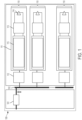
- the antenna power system 100 includes an AC/DC converter 101 that is receptive of AC, a common DC distribution bus 102 that is receptive of DC from the AC/DC converter 101 and a plurality of T/R channels 110.
- Each T/R channel 110 is responsible for T/R operations and includes a power amplification assembly 111 and a discrete input capacitor 112.
- the discrete input capacitor 112 is electrically interposed between the common DC distribution bus 102 and the power amplification assembly 111.
- the power amplification assembly 111 includes a discrete output capacitor 113, which is electrically interposed between a power amplifier 114 and an integrated DC/DC converter 115.
- the integrated DC/DC converter 115 may be provided as a galvanically-isolated bridge converter and includes shields extending into a transformer area as will be described below.
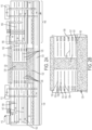
- the integrated DC/DC converter 115 includes a transformer area 120 that is interposed between an input section 130 and an output section 140.
- the input section 130 includes the discrete input capacitor 112 and the output section 140 includes the discrete output capacitor 113.
- the transformer area 120 includes a magnetic core top portion 121 that is formed of magnetic materials, a magnetic core bottom portion 122 that is disposed on a baseplate 123 and is formed of magnetic materials, a magnetic core pillar 124 that extends between central sections of the magnetic core top and bottom portions 121 and 122 and successive layers 125 at opposite sides of the magnetic core pillar 124.
- the successive layers 125 include layers of shield (i.e., metallic) and magnetic core materials, layers of windings and magnetic core materials and layers of shield and magnetic core materials, each of which are interleaved between dielectric material layers 126.
- the magnetic core top and bottom portions 121 and 122 have similar widths
- the magnetic core pillar 124 has a lesser width than the magnetic core top and bottom portions 121 and 122 and the successive layers 125 of the windings and the magnetic core materials extend outwardly to respective edges of the magnetic core top and bottom portions 121 and 122.
- the successive layers 125 include a layer of primary winding materials 150 and magnetic core materials 151 as well as a layer of first primary shield materials 152 and magnetic core materials 153 above the layer of the primary winding materials 150 and the magnetic core materials 151 and a layer of second primary shield materials 154 and magnetic core materials 155 below the layer of the primary winding materials 150 and the magnetic core materials 151.
- the successive layers 125 include a layer of secondary winding materials 156 and magnetic core materials 157 as well as a layer of first secondary shield materials 158 and magnetic core materials 159 above the layer of the secondary winding materials 156 and the magnetic core materials 157 and a layer of second secondary shield materials 160 and magnetic core materials 161 below the layer of the secondary winding materials 156 and the magnetic core materials 157.
- the layers of the first and second primary shield materials 152 and 154 extend continuously into the transformer area 120 from the discrete input capacitor 112 of the input section 130 and discontinuously correspond to layers of additional shield materials 162 (see FIG. 2A ) of the discrete output capacitor 113 in the output section 140.
- the layers of the first and second secondary shield materials 158 and 160 extend continuously into the transformer area 120 from the discrete output capacitor 113 of the output section 140 and discontinuously correspond to layers of additional shield materials 163 (see FIG. 2A ) of the discrete input capacitor 112 in the input section 130.
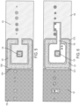
- the magnetic core materials 153 form a reverse C-shape about the magnetic core pillar 124.
- the magnetic core materials 153 are surrounded by dielectric materials 1530 and are adjacent to a line of dielectric materials 1531.
- the line of dielectric materials 1531 separates the first primary shield materials 152 from the layers of the additional shield materials 162.
- the layer of the second primary shield materials 154 and the magnetic core materials 155 below the layer of the primary winding materials 150 and the magnetic core materials 151 are similarly formed.
- the magnetic core materials 151 form a reverse C-shape about the magnetic core pillar 124.
- the magnetic core materials 151 are surrounded by dielectric materials 1510 and are adjacent to a line of dielectric materials 1511.
- the line of dielectric materials 1511 separates input capacitor shield materials 164 from output capacitor shield materials 165 (see FIG. 2A ).
- the magnetic core materials 159 form a C-shape about the magnetic core pillar 124.
- the magnetic core materials 159 are surrounded by dielectric materials 1590 and are adjacent to a line of dielectric materials 1591.
- the line of dielectric materials 1591 separates the first secondary shield materials 158 from the layers of the additional shield materials 163.
- the layer of the second secondary shield materials 160 and the magnetic core materials 161 below the layer of the secondary winding materials 156 and the magnetic core materials 157 are similarly formed.
- the magnetic core materials 157 form a C-shape about the magnetic core pillar 124.
- the magnetic core materials 157 are surrounded by dielectric materials 1570 and are adjacent to a line of dielectric materials 1571.
- the line of dielectric materials 1571 separates output capacitor shield materials 166 from input capacitor shield materials 167 (see FIG. 2A ).
- the output capacitor shield materials 165 may be similar materials as those of the layers of the first and second secondary shield materials 158 and 160.
- the input capacitor shield materials 167 may be similar materials as those of the layers of the first and second primary shield materials 152 and 154.
- all of the layers of the primary and secondary shield materials can occupy a same volume on separate layers only in the transformer area 120. This serves to reduce transformer feed-through capacitance (i.e., primary shields do not cross over to the secondary side and vice versa).
- layers of shield materials that are referenced to a highest DC voltage may be extended under the transformer area 120.
Landscapes
- Engineering & Computer Science (AREA)
- Power Engineering (AREA)
- Microelectronics & Electronic Packaging (AREA)
- Physics & Mathematics (AREA)
- Electromagnetism (AREA)
- Computer Networks & Wireless Communication (AREA)
- Dc-Dc Converters (AREA)
- Regulation Of General Use Transformers (AREA)
Description
- This invention was made with government support under contract number N00014-13-C-0231 awarded by United States Navy. The government has certain rights in the invention.
- The following description relates to a heterogeneously integrated power converter assembly and, more specifically, to an antenna power system with an integrated direct current (DC)/DC converter.
- In conventional antenna power systems for radar and other similar applications, there are typically massive numbers of off-array subsystems and electro-magnetic interference (EMI) filters that are required to achieve voltage quality. For example, a radar system can include a power distribution unit (PDU), an aperture power room (APR) for power conversion and distribution, multi-cable distribution and an array antenna.
- The PDU can include a 12-phase transformer that is required to provide a voltage step-down and a power factor correction (PFC) that is equal to a lower total harmonic distortion (THD). The APR can include a plurality of alternating current (AC)/DC converters that receive 12-phase 440 volt AC from the PDU. The multi-cable distribution can include a DC distribution bus that is receptive of DC from the AC/DC converters. The array antenna includes multiple antenna arrays.
- Each antenna array includes a number of transmit/receive integrated microwave module (T/RIMM) and multiple transmission/reception (T/R) channels. Each T/RIMM includes a plurality of linear regulators (one per T/R channel) and a DC/DC converter electrically interposed between the plurality of linear regulators and the DC distribution bus. The DC/DC converter serves to provide a voltage step-down, fast dynamic load response in T/R operations and reduces voltage ripples and noise. Each linear regulator provides for fast response and low noise point of load (POL) voltage. Each T/R channel is responsible for T/R operations and includes a power amplifier and a modulator electrically interposed between the power amplifier and a corresponding one of the linear regulators.
-
US 5,990,776 A discloses a multilayers structure in which all the magnetic elements have the windings edged in the inner layers and the magnetic core which surrounds the winding has the legs penetrating through the multilayers structure. The interconnection between the magnetic elements and the rest of electronic components are done through the layers of the multilayers board, horizontally and vertically through vias. -
US 5,602,554 A discloses a radar system which uses an active phased-array antenna achieves improved clutter improvement factor (CIF) by powering the various transmit-receive (TR) modules of the antenna with direct voltage (DC) derived from a plurality of phases of the power-line alternating current (AC). Each TR module receives power which originates with one phase of the source AC. The phases are selected so that the modulation of the radio-frequency (RF) signals by each TR module tends to cancel in the summed signal from the array antenna. -
US 2010/289610 A1 discloses an improved planar magnetic structure in which the voltage gradient between core and windings is reduced by shields disposed between the one or more legs of the core and the windings and extending through the PWB layers; vias are offset to permit them to be contained within the path of the winding; and the induced magnetic and eddy currents intrinsic to interstitial shield layers are reduced by configuring the shield conductors with pairs of courses with opposite and offsetting current propagation. - The present invention provides an integrated converter, as defined in claim 1. The present invention further provides an antenna power system, as defined in claim 8. Further optional features of the invention are defined in the dependent claims.
- The subject matter, which is regarded as the disclosure, is particularly pointed out and distinctly claimed in the claims at the conclusion of the specification. The foregoing and other features, and advantages of the disclosure are apparent from the following detailed description taken in conjunction with the accompanying drawings in which:
-
FIG. 1 is a schematic diagram of an antenna array power system in accordance with embodiments; -
FIG. 2A is a side view of an integrated DC/DC power converter for use in the antenna array power system ofFIG. 1 ; -
FIG. 2B is an enlarged side view of a transformer area of the integrated DC/DC power converter ofFIG. 2A ; -
FIG. 3 is a cross-sectional view taken along line 3-3 ofFIG. 2A ; -
FIG. 4 is a cross-sectional view taken along line 4-4 ofFIG. 2A ; -
FIG. 5 is a cross-sectional view taken along line 5-5 ofFIG. 2A ; and -
FIG. 6 is a cross-sectional view taken along line 6-6 ofFIG. 2A ; - These and other advantages and features will become more apparent from the following description taken in conjunction with the drawings.
- As will be described below, an architecture for an antenna array power system is provided with T/R module or channel-based DC/DC converters. This leads to a system that is simplified relative to conventional systems and universal T/RIMM elements that provide for greater portability when certain voltages (e.g., 300 VDC) are available from a common source. The architecture is characterized in that most of its power conversion components are disposed in the antenna array, which leads to a smaller, lighter and a higher performance and low cost system overall.
- In typical power conversion systems, common mode (CM) currents are generated by switching transitions and are coupled to an equipment ground by parasitic capacitance. At a load, the CM currents are converted into differential-mode ripples and noise. Meanwhile, differential (i.e., line-to-line) filters do not attenuate CM currents and an effectiveness of dedicated CM filters can be limited because CM currents often have wide ranges and high frequencies of up to hundreds of megahertz. Thus, it is often difficult to suppress CM currents without adding substantial electro-magnetic interference (EMI) filtering.
- In the presently claimed invention, however, high quality factor (Q) shield-to-transistor integrated low-inductance capacitor elements serve to divert CM currents, high Q shield-to-shield integrated low-inductance capacitor elements serve to compliment line-to-line filter capacitors and high Q baseplate integrated low-inductance capacitor elements serve to attenuate residual CM currents. This is achieved by integrated electrostatic shields being disposed to extend into a transformer area to contain CM currents by providing for low-inductance internal paths, the presence of "hybrid" magnetic cores that include discrete ("bulk") and integrated components to reduce magnetic reluctance and stray magnetic fields as well as composite dielectric layers that have low ε, high Q dielectrics windings of magnetics and high ε dielectrics for layers outside of the magnetics to reduce relative volumes of discrete capacitors.
- With reference to
FIG. 1 , anantenna power system 100 is provided. Theantenna power system 100 includes an AC/DC converter 101 that is receptive of AC, a commonDC distribution bus 102 that is receptive of DC from the AC/DC converter 101 and a plurality of T/R channels 110. Each T/R channel 110 is responsible for T/R operations and includes apower amplification assembly 111 and adiscrete input capacitor 112. Thediscrete input capacitor 112 is electrically interposed between the commonDC distribution bus 102 and thepower amplification assembly 111. Thepower amplification assembly 111 includes adiscrete output capacitor 113, which is electrically interposed between apower amplifier 114 and an integrated DC/DC converter 115. The integrated DC/DC converter 115 may be provided as a galvanically-isolated bridge converter and includes shields extending into a transformer area as will be described below. - With reference to
FIGS. 2A and 2B , components of the integrated DC/DC converter 115 are illustrated. As shown inFIG. 2A , the integrated DC/DC converter 115 includes atransformer area 120 that is interposed between aninput section 130 and anoutput section 140. Theinput section 130 includes thediscrete input capacitor 112 and theoutput section 140 includes thediscrete output capacitor 113. Thetransformer area 120 includes a magneticcore top portion 121 that is formed of magnetic materials, a magneticcore bottom portion 122 that is disposed on abaseplate 123 and is formed of magnetic materials, amagnetic core pillar 124 that extends between central sections of the magnetic core top andbottom portions successive layers 125 at opposite sides of themagnetic core pillar 124. Thesuccessive layers 125 include layers of shield (i.e., metallic) and magnetic core materials, layers of windings and magnetic core materials and layers of shield and magnetic core materials, each of which are interleaved between dielectric material layers 126. - In accordance with embodiments, the magnetic core top and
bottom portions magnetic core pillar 124 has a lesser width than the magnetic core top andbottom portions successive layers 125 of the windings and the magnetic core materials extend outwardly to respective edges of the magnetic core top andbottom portions - As shown in
FIG. 2B , thesuccessive layers 125 include a layer of primary windingmaterials 150 andmagnetic core materials 151 as well as a layer of firstprimary shield materials 152 andmagnetic core materials 153 above the layer of the primary windingmaterials 150 and themagnetic core materials 151 and a layer of secondprimary shield materials 154 andmagnetic core materials 155 below the layer of the primary windingmaterials 150 and themagnetic core materials 151. In addition, thesuccessive layers 125 include a layer of secondary windingmaterials 156 andmagnetic core materials 157 as well as a layer of firstsecondary shield materials 158 andmagnetic core materials 159 above the layer of the secondary windingmaterials 156 and themagnetic core materials 157 and a layer of secondsecondary shield materials 160 andmagnetic core materials 161 below the layer of the secondary windingmaterials 156 and themagnetic core materials 157. - The layers of the first and second
primary shield materials transformer area 120 from thediscrete input capacitor 112 of theinput section 130 and discontinuously correspond to layers of additional shield materials 162 (seeFIG. 2A ) of thediscrete output capacitor 113 in theoutput section 140. The layers of the first and secondsecondary shield materials transformer area 120 from thediscrete output capacitor 113 of theoutput section 140 and discontinuously correspond to layers of additional shield materials 163 (seeFIG. 2A ) of thediscrete input capacitor 112 in theinput section 130. - With reference to
FIG. 3 , in the layer of the firstprimary shield materials 152 and themagnetic core materials 153 above the layer of the primary windingmaterials 150 and themagnetic core materials 151, themagnetic core materials 153 form a reverse C-shape about themagnetic core pillar 124. In addition, themagnetic core materials 153 are surrounded bydielectric materials 1530 and are adjacent to a line ofdielectric materials 1531. The line ofdielectric materials 1531 separates the firstprimary shield materials 152 from the layers of theadditional shield materials 162. The layer of the secondprimary shield materials 154 and themagnetic core materials 155 below the layer of the primary windingmaterials 150 and themagnetic core materials 151 are similarly formed. - With reference to
FIG. 4 , in the layer of the primary windingmaterials 150 and themagnetic core materials 151, themagnetic core materials 151 form a reverse C-shape about themagnetic core pillar 124. In addition, themagnetic core materials 151 are surrounded bydielectric materials 1510 and are adjacent to a line ofdielectric materials 1511. The line ofdielectric materials 1511 separates inputcapacitor shield materials 164 from output capacitor shield materials 165 (seeFIG. 2A ). - With reference to
FIG. 5 , in the layer of the firstsecondary shield materials 158 and themagnetic core materials 159 above the layer of the secondary windingmaterials 156 and themagnetic core materials 157, themagnetic core materials 159 form a C-shape about themagnetic core pillar 124. In addition, themagnetic core materials 159 are surrounded bydielectric materials 1590 and are adjacent to a line ofdielectric materials 1591. The line ofdielectric materials 1591 separates the firstsecondary shield materials 158 from the layers of theadditional shield materials 163. The layer of the secondsecondary shield materials 160 and themagnetic core materials 161 below the layer of the secondary windingmaterials 156 and themagnetic core materials 157 are similarly formed. - With reference to
FIG. 6 , in the layer of the secondary windingmaterials 156 and themagnetic core materials 157, themagnetic core materials 157 form a C-shape about themagnetic core pillar 124. In addition, themagnetic core materials 157 are surrounded bydielectric materials 1570 and are adjacent to a line ofdielectric materials 1571. The line ofdielectric materials 1571 separates outputcapacitor shield materials 166 from input capacitor shield materials 167 (seeFIG. 2A ). - The output
capacitor shield materials 165 may be similar materials as those of the layers of the first and secondsecondary shield materials capacitor shield materials 167 may be similar materials as those of the layers of the first and secondprimary shield materials - In accordance with embodiment, all of the layers of the primary and secondary shield materials can occupy a same volume on separate layers only in the
transformer area 120. This serves to reduce transformer feed-through capacitance (i.e., primary shields do not cross over to the secondary side and vice versa). In addition, layers of shield materials that are referenced to a highest DC voltage (either primary or secondary) may be extended under thetransformer area 120. - The disclosure is not to be seen as limited by the foregoing description, but is only limited by the scope of the appended claims.
Claims (15)
- An integrated converter of an antenna power system (100), the integrated converter comprising:a baseplate (123);a transformer area (120) interposed between input and output sections (130, 140), the transformer area comprising:a magnetic core top portion (121);a magnetic core bottom portion (122) disposed on the baseplate (123);a magnetic core pillar (124) extending between central sections of the magnetic core top and bottom portions (122, 124); andsuccessive layers of shield and magnetic core materials (152, 153, 158, 159), windings and magnetic core materials (150, 151, 156, 157) and shield and magnetic core materials (154, 155, 160, 161) interleaved between dielectric material layers (126) at opposite sides of the magnetic core pillar (124), wherein the magnetic core materials (153, 155, 159, 161) in each successive layer of shield and magnetic core materials (153, 155, 159, 161, 152, 154, 158, 160) form a C-shape or a reverse C-shape about the magnetic core pillar (124).
- The integrated converter according to claim 1, wherein the integrated converter is provided as a galvanically-isolated bridge converter.
- The integrated converter according to claim 1, wherein the shield materials (154, 154, 158, 160) comprise metallic materials.
- The integrated converter according to claim 1, wherein:the magnetic core top and bottom portions (121, 122) have similar widths,the magnetic core pillar (124) has a lesser width than the magnetic core top and bottom portions (121, 122), andthe successive layers of the windings and the magnetic core materials (150, 151, 156, 157) extend outwardly to respective edges of the magnetic core top and bottom portions (121, 122).
- The integrated converter according to claim 1, wherein the successive layers comprise:primary winding materials (150);first and second primary shield materials (152, 154) above and below the primary winding materials (150);secondary winding materials (156); andfirst and second secondary shield materials (158, 160) above and below the secondary winding materials (156).
- The integrated converter according to claim 5, wherein:the first and second primary shield materials (154, 154) extend continuously into the transformer area (120) from the input section (130), andthe first and second secondary shield materials (158, 160) extend continuously into the transformer area from the output section (140).
- The integrated converter according to claim 5, wherein:the first and second primary shield materials (152, 154) discontinuously correspond to shield materials in the output section, andthe first and second secondary shield materials discontinuously correspond to shield materials in the input section (130).
- An antenna power system, comprising:an alternating current (AC)/direct current (DC) converter (101), which is receptive of AC;a common bus (102), which is receptive of DC from the AC/DC converter;a plurality of transmission/reception (T/R) channels (110) coupled to the common bus (102), each T/R channel (110) comprising:a power amplification assembly (111); anda discrete input capacitor (112) electrically interposed between the common bus (102) and the power amplification assembly (111),the power amplification assembly (111) comprising the integrated converter according to claim 1, a power amplifier, and a discrete output capacitor (113) electrically interposed between the power amplifier and the integrated converter as defined in claim 1, wherein the integrated converter is an integrated DC/DC converter (115) comprising shields extending into the transformer area.
- The antenna power system according to claim 8, wherein the integrated DC/DC converter (115) is provided as a galvanically-isolated bridge converter.
- The antenna power system according to claim 8, wherein the transformer area (120) of the integrated DC/DC converter (115) is interposed between an input section (113) comprising the discrete input capacitor (112) and an output section (140) comprising the discrete output capacitor (113).
- The antenna power system according to claim 8, wherein the shield materials (152, 154, 156, 157) comprise metallic materials.
- The antenna power system according to claim 8, wherein:the magnetic core top and bottom portions (121, 122) have similar widths, the magnetic core pillar (124) has a lesser width than the magnetic core top and bottom portions (121, 122), andthe successive layers of the windings and the magnetic core materials (150, 151, 156, 157) extend outwardly to respective edges of the magnetic core top and bottom portions (121, 122).
- The antenna power system according to claim 8, wherein the successive layers comprise:primary winding materials (150);first and second primary shield materials (152, 154) above and below the primary winding materials (150);secondary winding materials (156); andfirst and second secondary shield materials (158, 160) above and below the secondary winding materials (156).
- The antenna power system according to claim 13, wherein:the first and second primary shield materials (152, 154) extend continuously into the transformer area (120) from the discrete input capacitor (112), andthe first and second secondary shield materials (158, 160) extend continuously into the transformer area (120) from the discrete output capacitor (113).
- The antenna power system according to claim 13, wherein:the first and second primary shield materials (158, 160) discontinuously correspond to shield materials in the discrete output capacitor (113), andthe first and second secondary shield materials (158, 160) discontinuously correspond to shield materials in the discrete input capacitor (112).
Applications Claiming Priority (2)
| Application Number | Priority Date | Filing Date | Title |
|---|---|---|---|
| US201762542023P | 2017-08-07 | 2017-08-07 | |
| PCT/US2018/045359 WO2019032446A1 (en) | 2017-08-07 | 2018-08-06 | Hereterogenously integrated power converter assembly |
Publications (2)
| Publication Number | Publication Date |
|---|---|
| EP3665767A1 EP3665767A1 (en) | 2020-06-17 |
| EP3665767B1 true EP3665767B1 (en) | 2024-11-06 |
Family
ID=63364179
Family Applications (1)
| Application Number | Title | Priority Date | Filing Date |
|---|---|---|---|
| EP18759480.9A Active EP3665767B1 (en) | 2017-08-07 | 2018-08-06 | Heterogeneously integrated power converter assembly |
Country Status (4)
| Country | Link |
|---|---|
| US (2) | US10566896B2 (en) |
| EP (1) | EP3665767B1 (en) |
| JP (1) | JP6949199B2 (en) |
| WO (1) | WO2019032446A1 (en) |
Families Citing this family (2)
| Publication number | Priority date | Publication date | Assignee | Title |
|---|---|---|---|---|
| JP7391761B2 (en) * | 2020-05-15 | 2023-12-05 | キヤノン株式会社 | Power supply device and image forming device |
| CN115734464B (en) * | 2023-01-06 | 2023-05-05 | 四川斯艾普电子科技有限公司 | Thick film circuit substrate TR assembly and packaging method thereof |
Citations (2)
| Publication number | Priority date | Publication date | Assignee | Title |
|---|---|---|---|---|
| US20130242452A1 (en) * | 2010-11-09 | 2013-09-19 | Chan-Woong Park | Magnetic energy-transmitting element and power supply for cancelling out electrical noise |
| US20170110878A1 (en) * | 2015-10-16 | 2017-04-20 | Raytheon Company | Stacked power converter assembly |
Family Cites Families (27)
| Publication number | Priority date | Publication date | Assignee | Title |
|---|---|---|---|---|
| JPH06224043A (en) * | 1993-01-27 | 1994-08-12 | Taiyo Yuden Co Ltd | Laminated chip transformer and manufacture thereof |
| US5990776A (en) | 1994-12-08 | 1999-11-23 | Jitaru; Ionel | Low noise full integrated multilayers magnetic for power converters |
| US5602554A (en) * | 1995-08-08 | 1997-02-11 | Martin Marietta Corp. | Active array antenna with multiphase power for active modules |
| US6087922A (en) * | 1998-03-04 | 2000-07-11 | Astec International Limited | Folded foil transformer construction |
| US6054914A (en) * | 1998-07-06 | 2000-04-25 | Midcom, Inc. | Multi-layer transformer having electrical connection in a magnetic core |
| US6114939A (en) * | 1999-06-07 | 2000-09-05 | Technical Witts, Inc. | Planar stacked layer inductors and transformers |
| JP4415583B2 (en) | 2003-07-07 | 2010-02-17 | カシオ計算機株式会社 | Communication electronics, dictionary game program |
| AU2003266682A1 (en) * | 2003-09-29 | 2005-04-14 | Tamura Corporation | Laminated magnetic component and process for producing the same |
| JP4482765B2 (en) * | 2005-09-30 | 2010-06-16 | Tdk株式会社 | Switching power supply |
| IL188477A (en) * | 2007-12-27 | 2014-06-30 | Elta Systems Ltd | Power array for high power pulse load |
| US8928449B2 (en) * | 2008-05-28 | 2015-01-06 | Flextronics Ap, Llc | AC/DC planar transformer |
| JP5311462B2 (en) * | 2008-10-10 | 2013-10-09 | Fdk株式会社 | Multi-layer substrate transformer |
| US8089331B2 (en) | 2009-05-12 | 2012-01-03 | Raytheon Company | Planar magnetic structure |
| US8907447B2 (en) | 2010-02-19 | 2014-12-09 | Mingliang Wang | Power inductors in silicon |
| US8237535B2 (en) * | 2010-04-16 | 2012-08-07 | World Properties, Inc. | Integral planar transformer and busbar |
| JP2011258876A (en) * | 2010-06-11 | 2011-12-22 | Mitsubishi Electric Corp | High breakdown voltage flat transformer |
| US8461669B2 (en) | 2010-09-20 | 2013-06-11 | Monolithic Power Systems, Inc. | Integrated power converter package with die stacking |
| US8558344B2 (en) | 2011-09-06 | 2013-10-15 | Analog Devices, Inc. | Small size and fully integrated power converter with magnetics on chip |
| US20130328165A1 (en) | 2012-06-08 | 2013-12-12 | The Trustees Of Dartmouth College | Microfabricated magnetic devices and associated methods |
| US9847718B2 (en) | 2014-08-04 | 2017-12-19 | Ferric, Inc. | Apparatus and methods for integrated power converter with high bandwidth |
| US20150340422A1 (en) | 2014-05-23 | 2015-11-26 | Texas Instruments Incorporated | Method of manufacturing a micro-fabricated wafer level integrated inductor or transformer for high frequency switch mode power supplies |
| US9607748B2 (en) * | 2014-09-03 | 2017-03-28 | Teledyne Scientific & Imaging, Llc | Micro-fabricated integrated coil and magnetic circuit and method of manufacturing thereof |
| US9520793B2 (en) * | 2014-09-22 | 2016-12-13 | Raytheon Company | Stacked power converter assembly |
| JP6015813B2 (en) * | 2015-05-27 | 2016-10-26 | 株式会社村田製作所 | Multilayer circuit module |
| DE112016001457T5 (en) * | 2015-06-09 | 2017-12-14 | Google Llc | A POWER SUPPLY INCLUDING RETURN CONTROL AND DOWNWARD TRANSFORMER |
| US10049810B2 (en) * | 2015-11-09 | 2018-08-14 | Raytheon Company | High voltage high frequency transformer |
| TW201719963A (en) * | 2015-11-24 | 2017-06-01 | Prosperity Dielectrics Co Ltd | Impedance-matching converter of high-frequency transmission line formed of a carrier board, plural conductive copper pillars, an iron powder core, and a microstrip line inductor to effectively improve the inconvenience that automation is impossible with the winding-type inductor manufacturing process |
-
2018
- 2018-08-06 US US16/055,792 patent/US10566896B2/en active Active
- 2018-08-06 WO PCT/US2018/045359 patent/WO2019032446A1/en not_active Ceased
- 2018-08-06 EP EP18759480.9A patent/EP3665767B1/en active Active
- 2018-08-06 JP JP2020506769A patent/JP6949199B2/en active Active
-
2020
- 2020-01-13 US US16/741,318 patent/US11205953B2/en active Active
Patent Citations (2)
| Publication number | Priority date | Publication date | Assignee | Title |
|---|---|---|---|---|
| US20130242452A1 (en) * | 2010-11-09 | 2013-09-19 | Chan-Woong Park | Magnetic energy-transmitting element and power supply for cancelling out electrical noise |
| US20170110878A1 (en) * | 2015-10-16 | 2017-04-20 | Raytheon Company | Stacked power converter assembly |
Non-Patent Citations (2)
| Title |
|---|
| HARTLEY A C ET AL: "Large throw magnetic microactuator", MECHATRONICS, PERGAMON PRESS, OXFORD, GB, vol. 18, no. 9, 1 November 2008 (2008-11-01), pages 459 - 465, XP025472480, ISSN: 0957-4158, [retrieved on 20080727], DOI: 10.1016/J.MECHATRONICS.2008.05.012 * |
| OUYANG ZIWEI ET AL: "Overview of Planar Magnetic Technology-Fundamental Proper", IEEE TRANSACTIONS ON POWER ELECTRONICS, INSTITUTE OF ELECTRICAL AND ELECTRONICS ENGINEERS, USA, vol. 29, no. 9, 1 September 2014 (2014-09-01), pages 4888 - 4900, XP011546709, ISSN: 0885-8993, [retrieved on 20140430], DOI: 10.1109/TPEL.2013.2283263 * |
Also Published As
| Publication number | Publication date |
|---|---|
| US20190149039A1 (en) | 2019-05-16 |
| WO2019032446A1 (en) | 2019-02-14 |
| US20210273558A1 (en) | 2021-09-02 |
| EP3665767A1 (en) | 2020-06-17 |
| US10566896B2 (en) | 2020-02-18 |
| JP6949199B2 (en) | 2021-10-13 |
| US11205953B2 (en) | 2021-12-21 |
| JP2020530253A (en) | 2020-10-15 |
Similar Documents
| Publication | Publication Date | Title |
|---|---|---|
| CN108631292B (en) | active filter | |
| EP3696831B1 (en) | Planar transformer, power source switching circuit and adapter | |
| US9748036B2 (en) | Transformer | |
| US4888675A (en) | Switching power supply filter | |
| US9859867B2 (en) | Tunable LC filter | |
| US9941047B2 (en) | Shield for toroidal core electromagnetic device, and toroidal core electromagnetic devices utilizing such shields | |
| US7548137B2 (en) | Generalized cancellation of inductor winding capacitance | |
| US10340812B2 (en) | Flexible power converter architecture based on interposer and modular electronic units | |
| EP2007009A2 (en) | Planar emi filter | |
| EP2940701B1 (en) | Hybrid planar common-mode choke | |
| EP3665767B1 (en) | Heterogeneously integrated power converter assembly | |
| CN112366928A (en) | Voltage stabilizing circuit and device with ultralow ripple interference | |
| US8379415B2 (en) | Systems and methods for reducing EMI in switch mode converter systems | |
| US10049810B2 (en) | High voltage high frequency transformer | |
| US10886857B1 (en) | Inhibiting noise coupling across isolated power supplies | |
| CN210572692U (en) | Feed-through filter applied to magnetic resonance system and magnetic resonance system | |
| He et al. | Common-mode noise reduction in full-bridge LLC resonant converter with split primary winding transformer | |
| US20160234980A1 (en) | Electromagnetic Interference Suppressing Shield | |
| Cochrane | Passive cancellation of common-mode electromagnetic interference in switching power converters | |
| DE19812315A1 (en) | Noise suppression circuit for electronic revolution rate regulator | |
| US11694832B2 (en) | High voltage high frequency transformer | |
| EP3542378A1 (en) | Isolation transformer with low unwanted resonances, energy transfer device having an isolation transformer and energy transfer device for wireless transfer of energy having an isolation transformer | |
| US20260039278A1 (en) | Active compensation device providing electromagnetic wave noise data | |
| EP2249564B1 (en) | Electrical isolating device | |
| US6281777B1 (en) | Inductive component for the attenuation of common mode and push-pull interference |
Legal Events
| Date | Code | Title | Description |
|---|---|---|---|
| STAA | Information on the status of an ep patent application or granted ep patent |
Free format text: STATUS: UNKNOWN |
|
| STAA | Information on the status of an ep patent application or granted ep patent |
Free format text: STATUS: THE INTERNATIONAL PUBLICATION HAS BEEN MADE |
|
| PUAI | Public reference made under article 153(3) epc to a published international application that has entered the european phase |
Free format text: ORIGINAL CODE: 0009012 |
|
| STAA | Information on the status of an ep patent application or granted ep patent |
Free format text: STATUS: REQUEST FOR EXAMINATION WAS MADE |
|
| 17P | Request for examination filed |
Effective date: 20200203 |
|
| AK | Designated contracting states |
Kind code of ref document: A1 Designated state(s): AL AT BE BG CH CY CZ DE DK EE ES FI FR GB GR HR HU IE IS IT LI LT LU LV MC MK MT NL NO PL PT RO RS SE SI SK SM TR |
|
| AX | Request for extension of the european patent |
Extension state: BA ME |
|
| DAV | Request for validation of the european patent (deleted) | ||
| DAX | Request for extension of the european patent (deleted) | ||
| STAA | Information on the status of an ep patent application or granted ep patent |
Free format text: STATUS: EXAMINATION IS IN PROGRESS |
|
| 17Q | First examination report despatched |
Effective date: 20210416 |
|
| REG | Reference to a national code |
Ref country code: DE Ref legal event code: R079 Free format text: PREVIOUS MAIN CLASS: H02M0001440000 Ref country code: DE Ref legal event code: R079 Ref document number: 602018076279 Country of ref document: DE Free format text: PREVIOUS MAIN CLASS: H02M0001440000 Ipc: H01F0027360000 |
|
| GRAP | Despatch of communication of intention to grant a patent |
Free format text: ORIGINAL CODE: EPIDOSNIGR1 |
|
| STAA | Information on the status of an ep patent application or granted ep patent |
Free format text: STATUS: GRANT OF PATENT IS INTENDED |
|
| RIC1 | Information provided on ipc code assigned before grant |
Ipc: H05K 1/16 20060101ALI20240524BHEP Ipc: H01F 27/28 20060101ALI20240524BHEP Ipc: H02M 1/44 20070101ALI20240524BHEP Ipc: H01F 27/36 20060101AFI20240524BHEP |
|
| INTG | Intention to grant announced |
Effective date: 20240610 |
|
| GRAS | Grant fee paid |
Free format text: ORIGINAL CODE: EPIDOSNIGR3 |
|
| GRAA | (expected) grant |
Free format text: ORIGINAL CODE: 0009210 |
|
| STAA | Information on the status of an ep patent application or granted ep patent |
Free format text: STATUS: THE PATENT HAS BEEN GRANTED |
|
| AK | Designated contracting states |
Kind code of ref document: B1 Designated state(s): AL AT BE BG CH CY CZ DE DK EE ES FI FR GB GR HR HU IE IS IT LI LT LU LV MC MK MT NL NO PL PT RO RS SE SI SK SM TR |
|
| REG | Reference to a national code |
Ref country code: GB Ref legal event code: FG4D |
|
| REG | Reference to a national code |
Ref country code: CH Ref legal event code: EP |
|
| REG | Reference to a national code |
Ref country code: DE Ref legal event code: R096 Ref document number: 602018076279 Country of ref document: DE |
|
| REG | Reference to a national code |
Ref country code: IE Ref legal event code: FG4D |
|
| RAP4 | Party data changed (patent owner data changed or rights of a patent transferred) |
Owner name: RAYTHEON COMPANY |
|
| REG | Reference to a national code |
Ref country code: LT Ref legal event code: MG9D |
|
| REG | Reference to a national code |
Ref country code: NL Ref legal event code: MP Effective date: 20241106 |
|
| PG25 | Lapsed in a contracting state [announced via postgrant information from national office to epo] |
Ref country code: PT Free format text: LAPSE BECAUSE OF FAILURE TO SUBMIT A TRANSLATION OF THE DESCRIPTION OR TO PAY THE FEE WITHIN THE PRESCRIBED TIME-LIMIT Effective date: 20250306 Ref country code: HR Free format text: LAPSE BECAUSE OF FAILURE TO SUBMIT A TRANSLATION OF THE DESCRIPTION OR TO PAY THE FEE WITHIN THE PRESCRIBED TIME-LIMIT Effective date: 20241106 Ref country code: IS Free format text: LAPSE BECAUSE OF FAILURE TO SUBMIT A TRANSLATION OF THE DESCRIPTION OR TO PAY THE FEE WITHIN THE PRESCRIBED TIME-LIMIT Effective date: 20250306 |
|
| PG25 | Lapsed in a contracting state [announced via postgrant information from national office to epo] |
Ref country code: FI Free format text: LAPSE BECAUSE OF FAILURE TO SUBMIT A TRANSLATION OF THE DESCRIPTION OR TO PAY THE FEE WITHIN THE PRESCRIBED TIME-LIMIT Effective date: 20241106 Ref country code: NL Free format text: LAPSE BECAUSE OF FAILURE TO SUBMIT A TRANSLATION OF THE DESCRIPTION OR TO PAY THE FEE WITHIN THE PRESCRIBED TIME-LIMIT Effective date: 20241106 |
|
| REG | Reference to a national code |
Ref country code: AT Ref legal event code: MK05 Ref document number: 1740338 Country of ref document: AT Kind code of ref document: T Effective date: 20241106 |
|
| PG25 | Lapsed in a contracting state [announced via postgrant information from national office to epo] |
Ref country code: BG Free format text: LAPSE BECAUSE OF FAILURE TO SUBMIT A TRANSLATION OF THE DESCRIPTION OR TO PAY THE FEE WITHIN THE PRESCRIBED TIME-LIMIT Effective date: 20241106 |
|
| PG25 | Lapsed in a contracting state [announced via postgrant information from national office to epo] |
Ref country code: ES Free format text: LAPSE BECAUSE OF FAILURE TO SUBMIT A TRANSLATION OF THE DESCRIPTION OR TO PAY THE FEE WITHIN THE PRESCRIBED TIME-LIMIT Effective date: 20241106 |
|
| PG25 | Lapsed in a contracting state [announced via postgrant information from national office to epo] |
Ref country code: NO Free format text: LAPSE BECAUSE OF FAILURE TO SUBMIT A TRANSLATION OF THE DESCRIPTION OR TO PAY THE FEE WITHIN THE PRESCRIBED TIME-LIMIT Effective date: 20250206 |
|
| PG25 | Lapsed in a contracting state [announced via postgrant information from national office to epo] |
Ref country code: LV Free format text: LAPSE BECAUSE OF FAILURE TO SUBMIT A TRANSLATION OF THE DESCRIPTION OR TO PAY THE FEE WITHIN THE PRESCRIBED TIME-LIMIT Effective date: 20241106 Ref country code: GR Free format text: LAPSE BECAUSE OF FAILURE TO SUBMIT A TRANSLATION OF THE DESCRIPTION OR TO PAY THE FEE WITHIN THE PRESCRIBED TIME-LIMIT Effective date: 20250207 Ref country code: AT Free format text: LAPSE BECAUSE OF FAILURE TO SUBMIT A TRANSLATION OF THE DESCRIPTION OR TO PAY THE FEE WITHIN THE PRESCRIBED TIME-LIMIT Effective date: 20241106 |
|
| PG25 | Lapsed in a contracting state [announced via postgrant information from national office to epo] |
Ref country code: PL Free format text: LAPSE BECAUSE OF FAILURE TO SUBMIT A TRANSLATION OF THE DESCRIPTION OR TO PAY THE FEE WITHIN THE PRESCRIBED TIME-LIMIT Effective date: 20241106 |
|
| PG25 | Lapsed in a contracting state [announced via postgrant information from national office to epo] |
Ref country code: RS Free format text: LAPSE BECAUSE OF FAILURE TO SUBMIT A TRANSLATION OF THE DESCRIPTION OR TO PAY THE FEE WITHIN THE PRESCRIBED TIME-LIMIT Effective date: 20250206 |
|
| PG25 | Lapsed in a contracting state [announced via postgrant information from national office to epo] |
Ref country code: SM Free format text: LAPSE BECAUSE OF FAILURE TO SUBMIT A TRANSLATION OF THE DESCRIPTION OR TO PAY THE FEE WITHIN THE PRESCRIBED TIME-LIMIT Effective date: 20241106 |
|
| PG25 | Lapsed in a contracting state [announced via postgrant information from national office to epo] |
Ref country code: DK Free format text: LAPSE BECAUSE OF FAILURE TO SUBMIT A TRANSLATION OF THE DESCRIPTION OR TO PAY THE FEE WITHIN THE PRESCRIBED TIME-LIMIT Effective date: 20241106 |
|
| PG25 | Lapsed in a contracting state [announced via postgrant information from national office to epo] |
Ref country code: EE Free format text: LAPSE BECAUSE OF FAILURE TO SUBMIT A TRANSLATION OF THE DESCRIPTION OR TO PAY THE FEE WITHIN THE PRESCRIBED TIME-LIMIT Effective date: 20241106 |
|
| PG25 | Lapsed in a contracting state [announced via postgrant information from national office to epo] |
Ref country code: RO Free format text: LAPSE BECAUSE OF FAILURE TO SUBMIT A TRANSLATION OF THE DESCRIPTION OR TO PAY THE FEE WITHIN THE PRESCRIBED TIME-LIMIT Effective date: 20241106 |
|
| PG25 | Lapsed in a contracting state [announced via postgrant information from national office to epo] |
Ref country code: SK Free format text: LAPSE BECAUSE OF FAILURE TO SUBMIT A TRANSLATION OF THE DESCRIPTION OR TO PAY THE FEE WITHIN THE PRESCRIBED TIME-LIMIT Effective date: 20241106 |
|
| PG25 | Lapsed in a contracting state [announced via postgrant information from national office to epo] |
Ref country code: CZ Free format text: LAPSE BECAUSE OF FAILURE TO SUBMIT A TRANSLATION OF THE DESCRIPTION OR TO PAY THE FEE WITHIN THE PRESCRIBED TIME-LIMIT Effective date: 20241106 |
|
| REG | Reference to a national code |
Ref country code: DE Ref legal event code: R097 Ref document number: 602018076279 Country of ref document: DE |
|
| PG25 | Lapsed in a contracting state [announced via postgrant information from national office to epo] |
Ref country code: SE Free format text: LAPSE BECAUSE OF FAILURE TO SUBMIT A TRANSLATION OF THE DESCRIPTION OR TO PAY THE FEE WITHIN THE PRESCRIBED TIME-LIMIT Effective date: 20241106 |
|
| PLBE | No opposition filed within time limit |
Free format text: ORIGINAL CODE: 0009261 |
|
| STAA | Information on the status of an ep patent application or granted ep patent |
Free format text: STATUS: NO OPPOSITION FILED WITHIN TIME LIMIT |
|
| PGFP | Annual fee paid to national office [announced via postgrant information from national office to epo] |
Ref country code: DE Payment date: 20250724 Year of fee payment: 8 |
|
| 26N | No opposition filed |
Effective date: 20250807 |
|
| PGFP | Annual fee paid to national office [announced via postgrant information from national office to epo] |
Ref country code: IT Payment date: 20250723 Year of fee payment: 8 |
|
| PGFP | Annual fee paid to national office [announced via postgrant information from national office to epo] |
Ref country code: GB Payment date: 20250724 Year of fee payment: 8 |
|
| PGFP | Annual fee paid to national office [announced via postgrant information from national office to epo] |
Ref country code: FR Payment date: 20250723 Year of fee payment: 8 |
|
| REG | Reference to a national code |
Ref country code: CH Ref legal event code: H13 Free format text: ST27 STATUS EVENT CODE: U-0-0-H10-H13 (AS PROVIDED BY THE NATIONAL OFFICE) Effective date: 20260324 |
|
| PG25 | Lapsed in a contracting state [announced via postgrant information from national office to epo] |
Ref country code: MC Free format text: LAPSE BECAUSE OF FAILURE TO SUBMIT A TRANSLATION OF THE DESCRIPTION OR TO PAY THE FEE WITHIN THE PRESCRIBED TIME-LIMIT Effective date: 20241106 |
|
| PG25 | Lapsed in a contracting state [announced via postgrant information from national office to epo] |
Ref country code: LU Free format text: LAPSE BECAUSE OF NON-PAYMENT OF DUE FEES Effective date: 20250806 |
|
| PG25 | Lapsed in a contracting state [announced via postgrant information from national office to epo] |
Ref country code: CH Free format text: LAPSE BECAUSE OF NON-PAYMENT OF DUE FEES Effective date: 20250831 |