EP3665761B1 - Wireless power transmission with fractional timing resolution - Google Patents
Wireless power transmission with fractional timing resolution Download PDFInfo
- Publication number
- EP3665761B1 EP3665761B1 EP18844255.2A EP18844255A EP3665761B1 EP 3665761 B1 EP3665761 B1 EP 3665761B1 EP 18844255 A EP18844255 A EP 18844255A EP 3665761 B1 EP3665761 B1 EP 3665761B1
- Authority
- EP
- European Patent Office
- Prior art keywords
- coupled
- rising edge
- output
- circuit
- power
- Prior art date
- Legal status (The legal status is an assumption and is not a legal conclusion. Google has not performed a legal analysis and makes no representation as to the accuracy of the status listed.)
- Active
Links
Images

Classifications
-
- H—ELECTRICITY
- H02—GENERATION; CONVERSION OR DISTRIBUTION OF ELECTRIC POWER
- H02J—ELECTRIC POWER NETWORKS; CIRCUIT ARRANGEMENTS OR SYSTEMS FOR SUPPLYING OR DISTRIBUTING ELECTRIC POWER; SYSTEMS FOR STORING ELECTRIC ENERGY
- H02J50/00—Circuit arrangements or systems for wireless supply or distribution of electric power
- H02J50/20—Circuit arrangements or systems for wireless supply or distribution of electric power using microwaves or radio frequency waves
-
- H—ELECTRICITY
- H02—GENERATION; CONVERSION OR DISTRIBUTION OF ELECTRIC POWER
- H02J—ELECTRIC POWER NETWORKS; CIRCUIT ARRANGEMENTS OR SYSTEMS FOR SUPPLYING OR DISTRIBUTING ELECTRIC POWER; SYSTEMS FOR STORING ELECTRIC ENERGY
- H02J50/00—Circuit arrangements or systems for wireless supply or distribution of electric power
- H02J50/10—Circuit arrangements or systems for wireless supply or distribution of electric power using inductive coupling
-
- G—PHYSICS
- G06—COMPUTING OR CALCULATING; COUNTING
- G06F—ELECTRIC DIGITAL DATA PROCESSING
- G06F1/00—Details not covered by groups G06F3/00 - G06F13/00 and G06F21/00
- G06F1/04—Generating or distributing clock signals or signals derived directly therefrom
-
- G—PHYSICS
- G06—COMPUTING OR CALCULATING; COUNTING
- G06F—ELECTRIC DIGITAL DATA PROCESSING
- G06F1/00—Details not covered by groups G06F3/00 - G06F13/00 and G06F21/00
- G06F1/26—Power supply means, e.g. regulation thereof
- G06F1/266—Arrangements to supply power to external peripherals either directly from the computer or under computer control, e.g. supply of power through the communication port, computer controlled power-strips
-
- G—PHYSICS
- G06—COMPUTING OR CALCULATING; COUNTING
- G06F—ELECTRIC DIGITAL DATA PROCESSING
- G06F1/00—Details not covered by groups G06F3/00 - G06F13/00 and G06F21/00
- G06F1/26—Power supply means, e.g. regulation thereof
- G06F1/32—Means for saving power
- G06F1/3203—Power management, i.e. event-based initiation of a power-saving mode
- G06F1/3234—Power saving characterised by the action undertaken
- G06F1/324—Power saving characterised by the action undertaken by lowering clock frequency
-
- H—ELECTRICITY
- H02—GENERATION; CONVERSION OR DISTRIBUTION OF ELECTRIC POWER
- H02M—APPARATUS FOR CONVERSION BETWEEN AC AND AC, BETWEEN AC AND DC, OR BETWEEN DC AND DC, AND FOR USE WITH MAINS OR SIMILAR POWER SUPPLY SYSTEMS; CONVERSION OF DC OR AC INPUT POWER INTO SURGE OUTPUT POWER; CONTROL OR REGULATION THEREOF
- H02M3/00—Conversion of DC power input into DC power output
- H02M3/22—Conversion of DC power input into DC power output with intermediate conversion into AC
- H02M3/24—Conversion of DC power input into DC power output with intermediate conversion into AC by static converters
- H02M3/28—Conversion of DC power input into DC power output with intermediate conversion into AC by static converters using discharge tubes with control electrode or semiconductor devices with control electrode to produce the intermediate AC
- H02M3/325—Conversion of DC power input into DC power output with intermediate conversion into AC by static converters using discharge tubes with control electrode or semiconductor devices with control electrode to produce the intermediate AC using devices of a triode or a transistor type requiring continuous application of a control signal
- H02M3/335—Conversion of DC power input into DC power output with intermediate conversion into AC by static converters using discharge tubes with control electrode or semiconductor devices with control electrode to produce the intermediate AC using devices of a triode or a transistor type requiring continuous application of a control signal using semiconductor devices only
- H02M3/33507—Conversion of DC power input into DC power output with intermediate conversion into AC by static converters using discharge tubes with control electrode or semiconductor devices with control electrode to produce the intermediate AC using devices of a triode or a transistor type requiring continuous application of a control signal using semiconductor devices only with automatic control of the output voltage or current, e.g. flyback converters
-
- H—ELECTRICITY
- H02—GENERATION; CONVERSION OR DISTRIBUTION OF ELECTRIC POWER
- H02M—APPARATUS FOR CONVERSION BETWEEN AC AND AC, BETWEEN AC AND DC, OR BETWEEN DC AND DC, AND FOR USE WITH MAINS OR SIMILAR POWER SUPPLY SYSTEMS; CONVERSION OF DC OR AC INPUT POWER INTO SURGE OUTPUT POWER; CONTROL OR REGULATION THEREOF
- H02M3/00—Conversion of DC power input into DC power output
- H02M3/22—Conversion of DC power input into DC power output with intermediate conversion into AC
- H02M3/24—Conversion of DC power input into DC power output with intermediate conversion into AC by static converters
- H02M3/28—Conversion of DC power input into DC power output with intermediate conversion into AC by static converters using discharge tubes with control electrode or semiconductor devices with control electrode to produce the intermediate AC
- H02M3/325—Conversion of DC power input into DC power output with intermediate conversion into AC by static converters using discharge tubes with control electrode or semiconductor devices with control electrode to produce the intermediate AC using devices of a triode or a transistor type requiring continuous application of a control signal
- H02M3/335—Conversion of DC power input into DC power output with intermediate conversion into AC by static converters using discharge tubes with control electrode or semiconductor devices with control electrode to produce the intermediate AC using devices of a triode or a transistor type requiring continuous application of a control signal using semiconductor devices only
- H02M3/33507—Conversion of DC power input into DC power output with intermediate conversion into AC by static converters using discharge tubes with control electrode or semiconductor devices with control electrode to produce the intermediate AC using devices of a triode or a transistor type requiring continuous application of a control signal using semiconductor devices only with automatic control of the output voltage or current, e.g. flyback converters
- H02M3/33515—Conversion of DC power input into DC power output with intermediate conversion into AC by static converters using discharge tubes with control electrode or semiconductor devices with control electrode to produce the intermediate AC using devices of a triode or a transistor type requiring continuous application of a control signal using semiconductor devices only with automatic control of the output voltage or current, e.g. flyback converters with digital control
-
- H—ELECTRICITY
- H02—GENERATION; CONVERSION OR DISTRIBUTION OF ELECTRIC POWER
- H02M—APPARATUS FOR CONVERSION BETWEEN AC AND AC, BETWEEN AC AND DC, OR BETWEEN DC AND DC, AND FOR USE WITH MAINS OR SIMILAR POWER SUPPLY SYSTEMS; CONVERSION OF DC OR AC INPUT POWER INTO SURGE OUTPUT POWER; CONTROL OR REGULATION THEREOF
- H02M3/00—Conversion of DC power input into DC power output
- H02M3/22—Conversion of DC power input into DC power output with intermediate conversion into AC
- H02M3/24—Conversion of DC power input into DC power output with intermediate conversion into AC by static converters
- H02M3/28—Conversion of DC power input into DC power output with intermediate conversion into AC by static converters using discharge tubes with control electrode or semiconductor devices with control electrode to produce the intermediate AC
- H02M3/325—Conversion of DC power input into DC power output with intermediate conversion into AC by static converters using discharge tubes with control electrode or semiconductor devices with control electrode to produce the intermediate AC using devices of a triode or a transistor type requiring continuous application of a control signal
- H02M3/335—Conversion of DC power input into DC power output with intermediate conversion into AC by static converters using discharge tubes with control electrode or semiconductor devices with control electrode to produce the intermediate AC using devices of a triode or a transistor type requiring continuous application of a control signal using semiconductor devices only
- H02M3/33569—Conversion of DC power input into DC power output with intermediate conversion into AC by static converters using discharge tubes with control electrode or semiconductor devices with control electrode to produce the intermediate AC using devices of a triode or a transistor type requiring continuous application of a control signal using semiconductor devices only having several active switching elements
- H02M3/33576—Conversion of DC power input into DC power output with intermediate conversion into AC by static converters using discharge tubes with control electrode or semiconductor devices with control electrode to produce the intermediate AC using devices of a triode or a transistor type requiring continuous application of a control signal using semiconductor devices only having several active switching elements having at least one active switching element at the secondary side of an isolation transformer
-
- H—ELECTRICITY
- H02—GENERATION; CONVERSION OR DISTRIBUTION OF ELECTRIC POWER
- H02M—APPARATUS FOR CONVERSION BETWEEN AC AND AC, BETWEEN AC AND DC, OR BETWEEN DC AND DC, AND FOR USE WITH MAINS OR SIMILAR POWER SUPPLY SYSTEMS; CONVERSION OF DC OR AC INPUT POWER INTO SURGE OUTPUT POWER; CONTROL OR REGULATION THEREOF
- H02M3/00—Conversion of DC power input into DC power output
- H02M3/22—Conversion of DC power input into DC power output with intermediate conversion into AC
- H02M3/24—Conversion of DC power input into DC power output with intermediate conversion into AC by static converters
- H02M3/28—Conversion of DC power input into DC power output with intermediate conversion into AC by static converters using discharge tubes with control electrode or semiconductor devices with control electrode to produce the intermediate AC
- H02M3/325—Conversion of DC power input into DC power output with intermediate conversion into AC by static converters using discharge tubes with control electrode or semiconductor devices with control electrode to produce the intermediate AC using devices of a triode or a transistor type requiring continuous application of a control signal
- H02M3/335—Conversion of DC power input into DC power output with intermediate conversion into AC by static converters using discharge tubes with control electrode or semiconductor devices with control electrode to produce the intermediate AC using devices of a triode or a transistor type requiring continuous application of a control signal using semiconductor devices only
- H02M3/337—Conversion of DC power input into DC power output with intermediate conversion into AC by static converters using discharge tubes with control electrode or semiconductor devices with control electrode to produce the intermediate AC using devices of a triode or a transistor type requiring continuous application of a control signal using semiconductor devices only in push-pull configuration
- H02M3/3376—Conversion of DC power input into DC power output with intermediate conversion into AC by static converters using discharge tubes with control electrode or semiconductor devices with control electrode to produce the intermediate AC using devices of a triode or a transistor type requiring continuous application of a control signal using semiconductor devices only in push-pull configuration with automatic control of output voltage or current
-
- H—ELECTRICITY
- H03—ELECTRONIC CIRCUITRY
- H03L—AUTOMATIC CONTROL, STARTING, SYNCHRONISATION OR STABILISATION OF GENERATORS OF ELECTRONIC OSCILLATIONS OR PULSES
- H03L7/00—Automatic control of frequency or phase; Synchronisation
- H03L7/06—Automatic control of frequency or phase; Synchronisation using a reference signal applied to a frequency- or phase-locked loop
- H03L7/08—Details of the phase-locked loop
- H03L7/099—Details of the phase-locked loop concerning mainly the controlled oscillator of the loop
-
- H—ELECTRICITY
- H02—GENERATION; CONVERSION OR DISTRIBUTION OF ELECTRIC POWER
- H02J—ELECTRIC POWER NETWORKS; CIRCUIT ARRANGEMENTS OR SYSTEMS FOR SUPPLYING OR DISTRIBUTING ELECTRIC POWER; SYSTEMS FOR STORING ELECTRIC ENERGY
- H02J7/00—Circuit arrangements for charging or discharging batteries or for supplying loads from batteries
- H02J7/90—Regulation of charging or discharging current or voltage
- H02J7/933—Regulation of charging or discharging current or voltage the cycle being controlled or terminated in response to electric parameters
-
- H—ELECTRICITY
- H03—ELECTRONIC CIRCUITRY
- H03K—PULSE TECHNIQUE
- H03K3/00—Circuits for generating electric pulses; Monostable, bistable or multistable circuits
- H03K3/01—Details
- H03K3/011—Modifications of generator to compensate for variations in physical values, e.g. voltage, temperature
-
- Y—GENERAL TAGGING OF NEW TECHNOLOGICAL DEVELOPMENTS; GENERAL TAGGING OF CROSS-SECTIONAL TECHNOLOGIES SPANNING OVER SEVERAL SECTIONS OF THE IPC; TECHNICAL SUBJECTS COVERED BY FORMER USPC CROSS-REFERENCE ART COLLECTIONS [XRACs] AND DIGESTS
- Y02—TECHNOLOGIES OR APPLICATIONS FOR MITIGATION OR ADAPTATION AGAINST CLIMATE CHANGE
- Y02B—CLIMATE CHANGE MITIGATION TECHNOLOGIES RELATED TO BUILDINGS, e.g. HOUSING, HOUSE APPLIANCES OR RELATED END-USER APPLICATIONS
- Y02B40/00—Technologies aiming at improving the efficiency of home appliances, e.g. induction cooking or efficient technologies for refrigerators, freezers or dish washers
Definitions
- This relates generally to wireless power transmission, and more particularly to wireless power transmission with fractional timing resolution.
- a wireless power transmission system has a radio-frequency (RF) transmitter and an RF receiver.
- the RF transmitter is coupled to a source of electrical power (e.g., a mains power line), and it converts an electrical current into an oscillating electromagnetic field using an inductor, coil, antenna, metal plate, or other coupling device.
- a source of electrical power e.g., a mains power line
- Another coupling device at the RF receiver captures a portion of the radiated electromagnetic field (the two coils in proximity to each other form an electrical transformer), and the RF receiver then converts the received electromagnetic field back into an electrical current.
- the RF transmitter may be disposed within a charging pad or station, and the RF receiver may be coupled to a computing device (such as a desktop, laptop, tablet, smart phone, etc.) or a battery.
- a computing device such as a desktop, laptop, tablet, smart phone, etc.
- the energy transferred between the RF transmitter and the RF receiver may then be used to operate the computing device and/or to charge the battery.
- transfer efficiency (the amount of energy that is received relative to the amount of energy that is transmitted) is a critical parameter in wireless power transfer design.
- Coils in both the RF transmitter and the RF receiver are controlled using a number of switches or transistors, and increasing the power transfer efficiency often requires precise control of those transistors.
- the high-frequency clocks that would typically be necessary to provide such control would significantly increase cost and complexity.
- US 2017/0040988 A1 discloses a method and an apparatus for providing an adjustable high resolution dead time for e.g. a motor drive, audio amplifiers or computer power supplies.
- the implementation disclosed involve the use of counters, delay-locked loops and phase multiplexers.
- US 2017/0126069 A1 discloses controllers for wireless power systems including high-resolution pulse-width modulation involving the use of phase-locked loops, delay-locked loops and multiplexers.
- the invention is defined by the appended claims.
- the invention is directed in independent claim 1 to an electrical power transmitter.
- the invention is directed in dependent claim 7 to a wireless power transmission system including the electrical power transmitter of the first aspect.
- the invention is directed in independent claim 9 to a computing device comprising a wireless power receiver.
- the invention is directed in independent claim 13 to a method for receiving wireless power. Advantageous embodiments of the invention are defined by the remaining dependent claims.
- an electrical power transmitter may include a transistor and a rising edge control circuit configured to control a gate of the transistor to produce a rising edge of a pulse at a time selected with a resolution greater than a full-clock period.
- the electrical power transmitter may also comprise an inductor configured to emit power wireless over a power carrier frequency, where the full-clock period is the inverse of the power carrier frequency.
- the electrical power transmitter may also comprise a phased-locked loop (PLL) circuit having a voltage controlled oscillator (VCO), where the VCO is configured to produce a clock signal having a frequency n times greater than a power carrier frequency.
- PLL phased-locked loop
- VCO voltage controlled oscillator
- the rising edge control circuit may include a divider circuit coupled to the VCO and configured to divide the clock signal into n portions.
- the rising edge control circuit may also include a multiplexer coupled to the VCO and configured to subdivide each of the n portions into a plurality of m sub-portions.
- m may be a number of clock phases of the VCO.
- the rising edge control circuit may further comprise a delay circuit configured to apply a timing delay only to fewer than all possible m values.
- the resolution may be equal to the inverse of the power carrier frequency divided by a product of n times m.
- the gate of the transistor may be controlled via a falling edge control circuit that employs the power carrier frequency to produce a falling edge of the pulse at a subsequent time selected with the resolution.
- the wireless power transmitter further may include a flip-flop having a set input coupled to the rising edge control circuit and a reset input coupled to the falling edge control circuit, such that an output of the flip-flop is used to produce the pulse, and where the pulse is a pulse-width modulated (PWM) pulse usable to drive the gate of the transistor.
- PWM pulse-width modulated
- the electrical power transmitter may also include a receiver comprising: another inductor configured to receive the wireless power; and another transistor coupled to the other inductor, where another gate of the other transistor is controlled using another rising edge control circuit and another falling edge control circuit, and where the other rising edge control circuit and the other falling edge control circuit are configured to generate, using the power carrier frequency, another pulse having the resolution.
- the transistor may be part of an H-bridge circuit, and the other transistor may be part of a rectifier bridge.
- a computing device may include a processor and a wireless power receiver configured to provide power to the processor, where the wireless power receiver comprises an inductor coupled to a transistor, and where a gate of the transistor is controlled, in part, via a rising edge control circuit configured to employ a power carrier frequency to produce a rising edge of a pulse at a time selected with a resolution greater than an inverse of the power carrier frequency.
- the wireless power receiver may be configured to provide power to the processor by charging a battery.
- the transistor may be part of a rectifier circuit.
- the wireless power receiver further may include a VCO of a PLL circuit, wherein the VCO is configured to receive the power carrier frequency and to produce a clock signal having n times the power carrier frequency.
- the rising edge control circuit may include a divider coupled to the VCO and configured to split the clock signal into n portions; and a multiplexer coupled to the VCO and configured to subdivide each of the n portions into a plurality of m sub-portions, where m is a number of clock phases of the VCO, and where the resolution is equal to the inverse of the power carrier frequency divided by a product of n times m.
- the gate of the transistor may be further controlled, in part, via a falling edge control circuit configured to employ the power carrier frequency to produce a falling edge of the pulse at a subsequent time selected with the resolution, where the wireless power receiver further comprises a flip-flop having a set input coupled to the rising edge control circuit and a reset input coupled to the falling edge control circuit, and where an output of the flip-flop is usable to produce the pulse.
- a falling edge control circuit configured to employ the power carrier frequency to produce a falling edge of the pulse at a subsequent time selected with the resolution
- the wireless power receiver further comprises a flip-flop having a set input coupled to the rising edge control circuit and a reset input coupled to the falling edge control circuit, and where an output of the flip-flop is usable to produce the pulse.
- a method may include receiving electrical power wirelessly via an inductor over a power carrier frequency, where the inductor is coupled to a rectifier having a set of transistors; generating a PWM signal using one or more selected ones of n x m subdivisions of a VCO output produced by a VCO of a PLL circuit, where the VCO is configured to receive a reference clock having the power carrier frequency and to produce the output having n times the power carrier frequency and m selectable phases; and controlling each of the set of transistors with the PWM signal.
- the method may also include providing the power to a battery or computing device.
- FIG. 1 is a block diagram of an example wireless power transmission system 100. As shown, wireless power transmission system 100 includes radio frequency (RF) transmitter 101 and RF receiver 102.
- RF radio frequency
- RF transmitter 101 includes RF transmitter circuitry 103 and H-bridge 105 having a plurality of transistors or switches Q1-Q4.
- H-bridge refers to an electronic circuit that enables a voltage to be applied across a load in either direction.
- Transistors Q1-Q4 may each have a diode between source and drain terminals.
- Q1-Q4 may be implemented as power metal-oxide-semiconductor field-effect transistors (MOSFETs) or the like.
- MOSFETs power metal-oxide-semiconductor field-effect transistors
- RF transmitter 101 also includes primary smoothing capacitance (C primary ) and primary inductor, coil, or antenna (L primary ) coupled to H-bridge 105.
- C primary primary smoothing capacitance
- L primary primary inductor, coil, or antenna
- L secondary secondary inductor, coil, or antenna
- RF receiver 102 includes L secondary and secondary smoothing capacitance (C secondary ) coupled to rectifier bridge 106.
- Rectifier bridge 106 includes a plurality of transistors or switches Q4-Q8 (e.g ., power MOSFETs) coupled to RF receiver circuitry 104.
- the node between Q5 and Q8 provides an output voltage rail (V bridge_out ).
- V bridge_out is then provided to a buck-boost converter, voltage regulator, or the like (not shown), in order to power an electrical load, such as a battery or processor of a computing device.
- Electrical transformer 107 enables primary electric current I p to be converted into electromagnetic field M, which is then emitted by L primary as a power carrier signal having a power carrier frequency.
- L secondary receives a portion of the electromagnetic energy and converts it into secondary electric current I s .
- the efficiency of the power transfer between RF transmitter 101 and RF receiver 102 is given by the ratio between energy transmitted and energy received, which is proportional to the ratio between electrical currents I s and I p . Moreover, this efficiency is largely dependent upon the speed and precision with which transistors Q1-Q8 can be turned on (conductive) and off (non-conductive save for leakage effects), in order to generate I p and I s .
- transistors Q1-Q8 are controlled by RF transmitter circuitry 103 and RF receiver circuitry 104, which apply pulse signals to the gate terminals of their respective transistors.
- RF transmitter circuitry 103 and RF receiver circuitry 104 may produce pulse-width modulated (PWM) pulses having a timing resolution or granularity selected based upon a fractional division of a clock signal. For example, such a clock signal may the same frequency over which power is wirelessly radiated (power carrier frequency).
- PWM pulse-width modulated
- the power carrier frequency is over several Megahertz, such as 6.78 MHz
- the resolution or granularity for the gate driver pulses (on/off) should be in the 1.1 ns range.
- a system clock of 870 MHz would ordinarily be needed as a time basis for generating these pulses.
- operating at this high clock frequency would significantly increase the implementation cost and complexity of the final solution.
- a major cost adder is the fact that the required process and technology for implementing such a system needs to concurrently support both high voltage and high speed operation. This is usually not easy to achieve at an acceptable cost. Also, the resulting high power consumption is another factor which renders conventional implementations uncompetitive.
- fractional division of the clock signal may be achieved with a phase-locked loop (PPL) circuit coupled to one or more gate control circuits, as depicted in FIG. 2 .
- PPL phase-locked loop
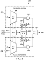
- FIG. 2 is a block diagram of PLL-based PWM pulse generator with fractional period timing resolution 200.
- generator 200 may be deployed in RF transmitter circuitry 103 and/or RF receiver circuitry 104.
- VCO voltage controlled oscillator
- PLL filter not shown
- VCO 203 receives, from a PLL filter (not shown), a signal locked to the power carrier frequency (e.g. , running 6.78 MHz).
- VCO 203 may be an m -stage fully differential ring oscillator (e.g ., an 8-stage oscillator running at 108.48 MHz).
- VCO 203 The output of VCO 203 is provided to divider circuit 204 (in this case, divides the clock period in 16 parts or "bins.”
- Rising edge control circuit 201 includes first multiplexer 205 configured to receive one of the m phases of VCO 203, and to select one a value of m ( e.g., based upon a 3-bit LSB portion of a control word).
- Counter selection circuit 206 selects one of the n bins from divider 204 ( e.g., based upon a 4-bit MSB portion of the control word).
- the outputs from multiplexer 205 and counter selection circuit 206 are combined by logic gate 207 to select a rise time for a PWM pulse with a time resolution or granularity (and/or in discrete time increments) equal to the period of the power carrier frequency divided by the product of n x m.
- falling edge control circuit 202 is similar to rising edge control circuit 201, in that multiplexer 208 may be another instance of the same device as multiplexer 205, and counter selection circuit 209 may be another instance of the same device as counter selection circuit 206.
- the output of logic gate 207 is coupled to the set input of flip-flop 211, and the output of logic gate 210 is coupled to the reset input of flip-flop 211. Accordingly, the resulting PWM pulse at the output of flip-flop 211 is produced with rising and falling edges selected with the aforementioned increased timing granularity or resolution.
- PLL-based PWM pulse generator 200 is capable of sub-nanosecond PWM pulse fidelity while running only at a 108.48 MHz system clock speed (from VCO 203). Fractional timing resolution may be achieved by tapping intermediate stages within an 8-stage ring oscillator. An all-digital gate-pulse encoder combines the ring oscillator clock phases with state information coming from the PLL feedback divider resulting in a high fidelity, extremely flexible PWM pulse generator.
- the PWM pulses driving the gates of NexFet devices Q1-Q8 are able to start anywhere and stop anywhere within a 1/6.78 MHz ( ⁇ 147 ns) reference clock cycle.
- VCO 203 is part of a PLL frequency synthesizer locked to an external reference clock running at 6.78MHz.
- the receiver side may use all of the same circuitry except that the 6.78MHz received carrier signal serves as the PLL reference.
- the pulse width of each of pulse may be controlled as the select of the decoder controlling the falling edge varies between 1 and 124 (7 bits of resolution).
- eight clock phases out of an 8-stage VCO ring oscillator may be combined with a 16 feedback divider (divide by 16) tap to generate PWM control pulses for all 4 gate/FET drivers on both transmitter (primary) and receiver (secondary) sides. Accordingly, the 147 ns (1/6.78 Mhz) reference clock cycle gets divided into 128 slots, each slot being 1.15 ns wide. Finally, the rising edge control output sets the SR FF (which starts the PWM pulse), whereas the falling edge control output resets the SR FF (which ends the PWM pulse).
- PWM width of 125-128 may not be coverable with circuit 200; but that is not necessary for this application. Yet, alternatively, the entire PWM width range may be covered.
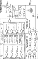
- FIG. 3 is a circuit diagram of implementation example 300 of PLL-based PWM generator with fractional period timing resolution 200.
- multiplexer circuit 301 MUX1
- multiplexer circuit 305 may implement multiplexers 206 and/or 208.
- Implementation example 300 also includes timing circuit 308 configured to operate upon a subset of phases selected via multiplexer 305 prior to being combined with the output of multiplexer circuit 301 via multiplexer 209 and in order to select a particular time for a rising or falling edge of the ultimate PWM pulse.
- Multiplexer circuit 301 includes a first set of logic gates 302 configured to select a first subset of the 16 bins (referred to as bins 0 through 15) resulting from operation of divider 204 using a two-bit portion of a 7-bit control word ( e.g ., bits 5 and 6).
- Multiplexer circuit 301 also includes a second set of logic gates 303 or multiplexers configured to select, within each of the subset of bins, a particular one of those bins using another two-bit portion of the 7-bit control word (e.g ., bits 3 and 4).
- the output of logic gates 302 and 303 are combined by logic gates 304 to select a specific one of the 16 bins by outputting a selected value of m.
- Multiplexer circuit 305 includes multiplexer 306 and multiplexer 307.
- Multiplexer 306 is operable to select one of phases 1, 2, 3, or 4 of VCO 203
- multiplexer 307 is operable to select one of phases 5, 6, 7, or 0.
- the value of n is set and multiplexer 309 issues a rising or falling edge at a time selected with increased resolution (e.g., 1.15 ns).
- timing circuit 308 may be used to adjust the timing of certain phase selections at the output of multiplexer 307 to avoid leakage effects or the like.
- multiplexer circuit 301 selects which one of the 16, CNTR feedback divider phases is used. All the CNTR phases come off the same tap of the VCO, namely VCO PHASE 0. Also, multiplexer circuit 301 gates the VCO phases 1, 2, 3, 4, which at this point can be directly ANDed with whichever COUNTER state is selected, given that the CNTR changes state on Phase 0. Meanwhile, multiplexer circuit 305 has 2 outputs: a first one is the MUXed phases 1, 2, 3, 4, which gets ANDed directly.
- the second output is the MUXed phases 5, 6, 7, 0, which take another route through clock re-timing circuit 308 in order to not create an unwanted double edge when the COUNTER selected state (clocked by VCO Phase 0) gets ANDed with the MUXed Phase 5, 6, 7, 0.
- clock re-timing circuit 308 may use the VCO phase 4 to resample the output and re-time it for subsequent VCO phases 5, 6, 7, 0. Again, this ensures that when VCO phases 5, 6, 7, 0 get ANDed-inside the clock re-timing circuit 308-with the selected and re-timed CNTR state, no double clock is occurring.
- multiplexer 309 selects (based on SELclk ⁇ 2>) which VCO Phase bank (1, 2, 3, 4 or 5, 6, 7, 0) goes to the final output.
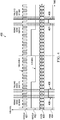
- FIG. 4 shows chart 400 illustrating the operation of PLL-based PWM generator with fractional period timing resolution 200.
- VCOCLK signal 401 is the clock signal output by VCO 203, which has 16x the power carrier frequency, shown as REFCLK signal 402 (e.g., 108.48 and 6.78 MHz, respectively).
- REFCLK signal 402 e.g., 108.48 and 6.78 MHz, respectively.
- the output of counter selector(s) 403 are bins 0-16 shown in gated curve 403.
- control word is a 7-bit word divided into two groups, which are: the four upper bits or MSBs; and the three lower bits or LSBs.
- the first group encodes a selected value for n (bin number 0->15) and the second portion encodes a selected value for m (phase 0->7).
- the first group is further subdivided into two parts: a first, 2-bit part that indicates a subset of bins, and a second, 2-bit part that indicates an individual bin within the subset.
- a first pulse has a rising edge 405 given by control word 0011010, in binary form.
- "00" indicates one of the four subset of bins (e.g., one of bins 0-4, in this case bin 0), and "01” pinpoints the third bin within that subset (in this case, bin 3).
- rising edge 405 may be placed at a precisely desired rise time.
- a subsequence pulse has a rising edge 407 and falling edge 408 selected by control words 1001110 and 1011001, respectively.
- analog implementations exist that rely on the counter, digital-to-analog converter (DAC), and comparator schemes to generate PWM pulses.
- DAC digital-to-analog converter
- comparator schemes to generate PWM pulses.
- these analog techniques suffer from limitations typically associated with analog circuits, such as poor component matching, drift over temperature, variation over process, higher power, potential instability, and/or reduced scalability.
- systems and methods described herein may provide a number of features, such as allowing cheaper and/or older technologies to employ high-voltage capabilities needed to drive the external NexFet devices. These systems and methods also use much less power given that the maximum frequency of operation is only 1/8 of the full-clock -based design (RMS power is proportional to the operating frequency).
- the proposed PWM generator provides superior performance without the need for background calibration or trimming.
- An all-digital implementation results in improved part-to-part matching, and consistent and repeatable performance across wide operating temperature ranges.
Landscapes
- Engineering & Computer Science (AREA)
- Theoretical Computer Science (AREA)
- Power Engineering (AREA)
- General Engineering & Computer Science (AREA)
- Physics & Mathematics (AREA)
- General Physics & Mathematics (AREA)
- Computer Networks & Wireless Communication (AREA)
- Computer Hardware Design (AREA)
- Stabilization Of Oscillater, Synchronisation, Frequency Synthesizers (AREA)
- Charge And Discharge Circuits For Batteries Or The Like (AREA)
- Dc-Dc Converters (AREA)
- Pulse Circuits (AREA)
Description
- This relates generally to wireless power transmission, and more particularly to wireless power transmission with fractional timing resolution.
- A wireless power transmission system has a radio-frequency (RF) transmitter and an RF receiver. The RF transmitter is coupled to a source of electrical power (e.g., a mains power line), and it converts an electrical current into an oscillating electromagnetic field using an inductor, coil, antenna, metal plate, or other coupling device. Another coupling device at the RF receiver captures a portion of the radiated electromagnetic field (the two coils in proximity to each other form an electrical transformer), and the RF receiver then converts the received electromagnetic field back into an electrical current.
- In many implementations, the RF transmitter may be disposed within a charging pad or station, and the RF receiver may be coupled to a computing device (such as a desktop, laptop, tablet, smart phone, etc.) or a battery. The energy transferred between the RF transmitter and the RF receiver may then be used to operate the computing device and/or to charge the battery. Hence, transfer efficiency (the amount of energy that is received relative to the amount of energy that is transmitted) is a critical parameter in wireless power transfer design.
- Coils in both the RF transmitter and the RF receiver are controlled using a number of switches or transistors, and increasing the power transfer efficiency often requires precise control of those transistors. However, the high-frequency clocks that would typically be necessary to provide such control would significantly increase cost and complexity.
-
US 2017/0040988 A1 discloses a method and an apparatus for providing an adjustable high resolution dead time for e.g. a motor drive, audio amplifiers or computer power supplies. The implementation disclosed involve the use of counters, delay-locked loops and phase multiplexers. -
US 2017/0126069 A1 discloses controllers for wireless power systems including high-resolution pulse-width modulation involving the use of phase-locked loops, delay-locked loops and multiplexers. - The invention is defined by the appended claims. In a first aspect, the invention is directed in
independent claim 1 to an electrical power transmitter. In a second aspect, the invention is directed in dependent claim 7 to a wireless power transmission system including the electrical power transmitter of the first aspect. In a third aspect, the invention is directed inindependent claim 9 to a computing device comprising a wireless power receiver. In a fourth aspect, the invention is directed inindependent claim 13 to a method for receiving wireless power. Advantageous embodiments of the invention are defined by the remaining dependent claims. - In described examples of systems and methods for wireless power transfer with fractional timing resolution, an electrical power transmitter may include a transistor and a rising edge control circuit configured to control a gate of the transistor to produce a rising edge of a pulse at a time selected with a resolution greater than a full-clock period.
- The electrical power transmitter may also comprise an inductor configured to emit power wireless over a power carrier frequency, where the full-clock period is the inverse of the power carrier frequency. The electrical power transmitter may also comprise a phased-locked loop (PLL) circuit having a voltage controlled oscillator (VCO), where the VCO is configured to produce a clock signal having a frequency n times greater than a power carrier frequency.
- In some cases, the rising edge control circuit may include a divider circuit coupled to the VCO and configured to divide the clock signal into n portions. The rising edge control circuit may also include a multiplexer coupled to the VCO and configured to subdivide each of the n portions into a plurality of m sub-portions. For example, m may be a number of clock phases of the VCO. The rising edge control circuit may further comprise a delay circuit configured to apply a timing delay only to fewer than all possible m values. The resolution may be equal to the inverse of the power carrier frequency divided by a product of n times m.
- In some implementations, the gate of the transistor may be controlled via a falling edge control circuit that employs the power carrier frequency to produce a falling edge of the pulse at a subsequent time selected with the resolution. The wireless power transmitter further may include a flip-flop having a set input coupled to the rising edge control circuit and a reset input coupled to the falling edge control circuit, such that an output of the flip-flop is used to produce the pulse, and where the pulse is a pulse-width modulated (PWM) pulse usable to drive the gate of the transistor.
- The electrical power transmitter may also include a receiver comprising: another inductor configured to receive the wireless power; and another transistor coupled to the other inductor, where another gate of the other transistor is controlled using another rising edge control circuit and another falling edge control circuit, and where the other rising edge control circuit and the other falling edge control circuit are configured to generate, using the power carrier frequency, another pulse having the resolution. The transistor may be part of an H-bridge circuit, and the other transistor may be part of a rectifier bridge.
- Additionally, a computing device may include a processor and a wireless power receiver configured to provide power to the processor, where the wireless power receiver comprises an inductor coupled to a transistor, and where a gate of the transistor is controlled, in part, via a rising edge control circuit configured to employ a power carrier frequency to produce a rising edge of a pulse at a time selected with a resolution greater than an inverse of the power carrier frequency.
- The wireless power receiver may be configured to provide power to the processor by charging a battery. The transistor may be part of a rectifier circuit. And the wireless power receiver further may include a VCO of a PLL circuit, wherein the VCO is configured to receive the power carrier frequency and to produce a clock signal having n times the power carrier frequency.
- The rising edge control circuit may include a divider coupled to the VCO and configured to split the clock signal into n portions; and a multiplexer coupled to the VCO and configured to subdivide each of the n portions into a plurality of m sub-portions, where m is a number of clock phases of the VCO, and where the resolution is equal to the inverse of the power carrier frequency divided by a product of n times m. The gate of the transistor may be further controlled, in part, via a falling edge control circuit configured to employ the power carrier frequency to produce a falling edge of the pulse at a subsequent time selected with the resolution, where the wireless power receiver further comprises a flip-flop having a set input coupled to the rising edge control circuit and a reset input coupled to the falling edge control circuit, and where an output of the flip-flop is usable to produce the pulse.
- Additionally, a method may include receiving electrical power wirelessly via an inductor over a power carrier frequency, where the inductor is coupled to a rectifier having a set of transistors; generating a PWM signal using one or more selected ones of n x m subdivisions of a VCO output produced by a VCO of a PLL circuit, where the VCO is configured to receive a reference clock having the power carrier frequency and to produce the output having n times the power carrier frequency and m selectable phases; and controlling each of the set of transistors with the PWM signal. The method may also include providing the power to a battery or computing device.
-
-
FIG. 1 is a block diagram of a wireless power transmission system. -
FIG. 2 is a block diagram of a phased-locked loop (PLL)-based pulse-width modulation (PWM) generator with fractional period timing resolution. -
FIG. 3 is a circuit diagram of a PLL-based PWM generator with fractional period timing resolution. -
FIG. 4 is a chart illustrating the operation of a PLL-based PWM generator with fractional period timing resolution. -
FIG. 1 is a block diagram of an example wirelesspower transmission system 100. As shown, wirelesspower transmission system 100 includes radio frequency (RF)transmitter 101 andRF receiver 102. -
RF transmitter 101 includesRF transmitter circuitry 103 and H-bridge 105 having a plurality of transistors or switches Q1-Q4. As used herein, the term "H-bridge" refers to an electronic circuit that enables a voltage to be applied across a load in either direction. Transistors Q1-Q4 may each have a diode between source and drain terminals. For example, Q1-Q4 may be implemented as power metal-oxide-semiconductor field-effect transistors (MOSFETs) or the like. -
RF transmitter 101 also includes primary smoothing capacitance (Cprimary) and primary inductor, coil, or antenna (Lprimary) coupled to H-bridge 105. When Lprimary is electromagnetically coupled to a secondary inductor, coil, or antenna (Lsecondary), it formselectrical transformer 107. -
RF receiver 102 includes Lsecondary and secondary smoothing capacitance (Csecondary) coupled torectifier bridge 106.Rectifier bridge 106 includes a plurality of transistors or switches Q4-Q8 (e.g., power MOSFETs) coupled toRF receiver circuitry 104. The node between Q5 and Q8 provides an output voltage rail (Vbridge_out). Vbridge_out is then provided to a buck-boost converter, voltage regulator, or the like (not shown), in order to power an electrical load, such as a battery or processor of a computing device. -
Electrical transformer 107 enables primary electric current Ip to be converted into electromagnetic field M, which is then emitted by Lprimary as a power carrier signal having a power carrier frequency. In turn, Lsecondary receives a portion of the electromagnetic energy and converts it into secondary electric current Is. - The efficiency of the power transfer between
RF transmitter 101 andRF receiver 102 is given by the ratio between energy transmitted and energy received, which is proportional to the ratio between electrical currents Is and Ip. Moreover, this efficiency is largely dependent upon the speed and precision with which transistors Q1-Q8 can be turned on (conductive) and off (non-conductive save for leakage effects), in order to generate Ip and Is. - Broadly, transistors Q1-Q8 are controlled by
RF transmitter circuitry 103 andRF receiver circuitry 104, which apply pulse signals to the gate terminals of their respective transistors.RF transmitter circuitry 103 andRF receiver circuitry 104 may produce pulse-width modulated (PWM) pulses having a timing resolution or granularity selected based upon a fractional division of a clock signal. For example, such a clock signal may the same frequency over which power is wirelessly radiated (power carrier frequency). - For example, if the power carrier frequency is over several Megahertz, such as 6.78 MHz, then the resolution or granularity for the gate driver pulses (on/off) should be in the 1.1 ns range. Given this requirement, a system clock of 870 MHz would ordinarily be needed as a time basis for generating these pulses. However, operating at this high clock frequency would significantly increase the implementation cost and complexity of the final solution. A major cost adder is the fact that the required process and technology for implementing such a system needs to concurrently support both high voltage and high speed operation. This is usually not easy to achieve at an acceptable cost. Also, the resulting high power consumption is another factor which renders conventional implementations uncompetitive.
- Accordingly, fractional division of the clock signal may be achieved with a phase-locked loop (PPL) circuit coupled to one or more gate control circuits, as depicted in
FIG. 2 . Particularly,FIG. 2 is a block diagram of PLL-based PWM pulse generator with fractionalperiod timing resolution 200. One or more instances ofgenerator 200 may be deployed inRF transmitter circuitry 103 and/orRF receiver circuitry 104. - As shown, voltage controlled oscillator (VCO) 203 receives, from a PLL filter (not shown), a signal locked to the power carrier frequency (e.g., running 6.78 MHz). In response,
VCO 203 produces a clock having a frequency n times greater the power carrier frequency (e.g., if n = 16, then the output clock frequency ofVCO 203 is 108.48 MHz). In some implementations,VCO 203 may be an m-stage fully differential ring oscillator (e.g., an 8-stage oscillator running at 108.48 MHz). - The output of
VCO 203 is provided to divider circuit 204 (in this case, divides the clock period in 16 parts or "bins." Risingedge control circuit 201 includesfirst multiplexer 205 configured to receive one of the m phases ofVCO 203, and to select one a value of m (e.g., based upon a 3-bit LSB portion of a control word).Counter selection circuit 206 selects one of the n bins from divider 204 (e.g., based upon a 4-bit MSB portion of the control word). The outputs frommultiplexer 205 andcounter selection circuit 206 are combined bylogic gate 207 to select a rise time for a PWM pulse with a time resolution or granularity (and/or in discrete time increments) equal to the period of the power carrier frequency divided by the product of n x m. - Particularly, in the case where the frequency is 6.78 MHz, the period of the power carrier signal is ∼147 ns; yet when n = 16 and m = 8, the timing resolution for the selected rise time is in the order of 1.15 ns.
- Still referring to
FIG. 2 , fallingedge control circuit 202 is similar to risingedge control circuit 201, in thatmultiplexer 208 may be another instance of the same device asmultiplexer 205, andcounter selection circuit 209 may be another instance of the same device ascounter selection circuit 206. - The output of
logic gate 207 is coupled to the set input of flip-flop 211, and the output oflogic gate 210 is coupled to the reset input of flip-flop 211. Accordingly, the resulting PWM pulse at the output of flip-flop 211 is produced with rising and falling edges selected with the aforementioned increased timing granularity or resolution. - PLL-based
PWM pulse generator 200 is capable of sub-nanosecond PWM pulse fidelity while running only at a 108.48 MHz system clock speed (from VCO 203). Fractional timing resolution may be achieved by tapping intermediate stages within an 8-stage ring oscillator. An all-digital gate-pulse encoder combines the ring oscillator clock phases with state information coming from the PLL feedback divider resulting in a high fidelity, extremely flexible PWM pulse generator. - The result is a PWM generation scheme with a 1.15 ns resolution for both pulse width and location. Thus, the PWM pulses driving the gates of NexFet devices Q1-Q8 (on both transmitter and synchronous receiver/rectifier) are able to start anywhere and stop anywhere within a 1/6.78 MHz (∼147 ns) reference clock cycle.
- On the transmitter side,
VCO 203 is part of a PLL frequency synthesizer locked to an external reference clock running at 6.78MHz. The receiver side may use all of the same circuitry except that the 6.78MHz received carrier signal serves as the PLL reference. - In some implementations, the circuit may yield the rising edge of the PWM pulse any start time (e.g., always at t = 150 ns), while the falling edge may be selected at any discrete time from t = 150 ns + 1.15 ns to t = 150 ns + 1.15 ns x 124 = 292 ns. The pulse width of each of pulse may be controlled as the select of the decoder controlling the falling edge varies between 1 and 124 (7 bits of resolution).
- For example, eight clock phases out of an 8-stage VCO ring oscillator may be combined with a 16 feedback divider (divide by 16) tap to generate PWM control pulses for all 4 gate/FET drivers on both transmitter (primary) and receiver (secondary) sides. Accordingly, the 147 ns (1/6.78 Mhz) reference clock cycle gets divided into 128 slots, each slot being 1.15 ns wide. Finally, the rising edge control output sets the SR FF (which starts the PWM pulse), whereas the falling edge control output resets the SR FF (which ends the PWM pulse).
- Depending upon the speed limitations of the choice of process node, PWM width of 125-128 may not be coverable with
circuit 200; but that is not necessary for this application. Yet, alternatively, the entire PWM width range may be covered. -
FIG. 3 is a circuit diagram of implementation example 300 of PLL-based PWM generator with fractionalperiod timing resolution 200. Here, multiplexer circuit 301 (MUX1) may implementcounter selectors 206 and/or 209, andmultiplexer circuit 305 may implementmultiplexers 206 and/or 208. Implementation example 300 also includestiming circuit 308 configured to operate upon a subset of phases selected viamultiplexer 305 prior to being combined with the output ofmultiplexer circuit 301 viamultiplexer 209 and in order to select a particular time for a rising or falling edge of the ultimate PWM pulse. -
Multiplexer circuit 301 includes a first set oflogic gates 302 configured to select a first subset of the 16 bins (referred to asbins 0 through 15) resulting from operation ofdivider 204 using a two-bit portion of a 7-bit control word (e.g.,bits 5 and 6). Here, each of the subsets of bins has 4 coarse subdivisions: SEL counters = 0->3, 4->7, 8->11, or 12->15. -
Multiplexer circuit 301 also includes a second set oflogic gates 303 or multiplexers configured to select, within each of the subset of bins, a particular one of those bins using another two-bit portion of the 7-bit control word (e.g.,bits 3 and 4). Here, COUNTER decode inputs are again dispersed into different groups: COUNTER decode = 0->3, 4->7, 8->11, or 12->15, each COUNTER decode input selecting an individual bin within that subset of bins (finer or more precise selection). Finally, the output oflogic gates logic gates 304 to select a specific one of the 16 bins by outputting a selected value of m. -
Multiplexer circuit 305 includesmultiplexer 306 and multiplexer 307.Multiplexer 306 is operable to select one ofphases VCO 203, and multiplexer 307 is operable to select one ofphases timing circuit 308 may be used to adjust the timing of certain phase selections at the output of multiplexer 307 to avoid leakage effects or the like. - Accordingly,
multiplexer circuit 301 selects which one of the 16, CNTR feedback divider phases is used. All the CNTR phases come off the same tap of the VCO, namelyVCO PHASE 0. Also,multiplexer circuit 301 gates the VCO phases 1, 2, 3, 4, which at this point can be directly ANDed with whichever COUNTER state is selected, given that the CNTR changes state onPhase 0. Meanwhile,multiplexer circuit 305 has 2 outputs: a first one is the MUXed phases 1, 2, 3, 4, which gets ANDed directly. The second output is the MUXed phases 5, 6, 7, 0, which take another route throughclock re-timing circuit 308 in order to not create an unwanted double edge when the COUNTER selected state (clocked by VCO Phase 0) gets ANDed with theMUXed Phase - In some cases,
clock re-timing circuit 308 may use theVCO phase 4 to resample the output and re-time it for subsequent VCO phases 5, 6, 7, 0. Again, this ensures that when VCO phases 5, 6, 7, 0 get ANDed-inside the clock re-timing circuit 308-with the selected and re-timed CNTR state, no double clock is occurring. Finally, multiplexer 309 selects (based on SELclk<2>) which VCO Phase bank (1, 2, 3, 4 or 5, 6, 7, 0) goes to the final output. -
FIG. 4 shows chart 400 illustrating the operation of PLL-based PWM generator with fractionalperiod timing resolution 200.VCOCLK signal 401 is the clock signal output byVCO 203, which has 16x the power carrier frequency, shown as REFCLK signal 402 (e.g., 108.48 and 6.78 MHz, respectively). The output of counter selector(s) 403 are bins 0-16 shown ingated curve 403. - In at least one example, the control word is a 7-bit word divided into two groups, which are: the four upper bits or MSBs; and the three lower bits or LSBs. The first group encodes a selected value for n (bin number 0->15) and the second portion encodes a selected value for m (phase 0->7). Moreover, the first group is further subdivided into two parts: a first, 2-bit part that indicates a subset of bins, and a second, 2-bit part that indicates an individual bin within the subset.
- In this example, a first pulse has a rising
edge 405 given bycontrol word 0011010, in binary form. In sequential order from left to right, in the 4 MSBs, "00" indicates one of the four subset of bins (e.g., one of bins 0-4, in this case bin 0), and "01" pinpoints the third bin within that subset (in this case, bin 3). Moreover, in the 3 LSBs, "010" indicates the intra-bin subdivision (m = 2). - The pulse then has a falling
edge 406 selected bycontrol word 0101110 which, precisely places it at the 6th intra-bin subdivision (m = 6) of bin 5 (n = 5). Thus, using the granularity afforded by systems and methods described herein, risingedge 405 may be placed at a precisely desired rise time. - At a later time, a subsequence pulse has a rising
edge 407 and fallingedge 408 selected bycontrol words edge 405 is placed at the 6th intra-bin subdivision (m = 6) of bin 9 (n = 9), and fallingedge 408 is placed at the first intra-bin subdivision (m = 1) of bin 11 (n = 11). - In contrast with systems and methods described herein, conventional solutions to the foregoing problems fall in one of two categories. First, digital PWM generators exist that invariably rely on a PLL/DLL type implementation with synchronous PWM generation. These implementations require a system clock running at the rate proportional to the required PWM resolution (such as 870 MHz for a ∼1.15 ns timing resolution). Moreover, these implementations suffer from high implementation cost, high power consumption and increased complexity.
- Second, analog implementations exist that rely on the counter, digital-to-analog converter (DAC), and comparator schemes to generate PWM pulses. However, these analog techniques suffer from limitations typically associated with analog circuits, such as poor component matching, drift over temperature, variation over process, higher power, potential instability, and/or reduced scalability.
- Also, compared to full-clocked -based designs (such as where the VCO runs at 1/1.15 ns = 870 Mhz), systems and methods described herein may provide a number of features, such as allowing cheaper and/or older technologies to employ high-voltage capabilities needed to drive the external NexFet devices. These systems and methods also use much less power given that the maximum frequency of operation is only 1/8 of the full-clock -based design (RMS power is proportional to the operating frequency).
- Compared with traditional analog PWM generation schemes, the proposed PWM generator provides superior performance without the need for background calibration or trimming. An all-digital implementation results in improved part-to-part matching, and consistent and repeatable performance across wide operating temperature ranges. These systems and methods are flexible and scalable to any desirable PWM and/or reference frequency.
- Modifications are possible in the teachings of the above description and they belong to the invention if they fall within the scope of the claims.
Claims (14)
- An electrical power transmitter (101), comprising:a primary inductor (Lprimary);a drive transistor (Q1-Q4) coupled to the primary inductor, the transistor having a gate; anda rising edge control circuit (201) includinga voltage controlled oscillator, VCO, having a power carrier frequency input, configured to generate m stage outputs, and configured to generate a clock signal output at a frequency n times greater than the power carrier frequency;a rising edge multiplexer (205) having m sub-portion inputs coupled to the m stage outputs, a select input, and a rising edge multiplexer output;a rising edge divider circuit (204) having an input coupled to the clock signal output and having n rising edge portion outputs; andrising edge logic circuitry (207) having inputs coupled to the rising edge multiplexer output and the n rising edge portion outputs, and having a rising edge control output coupled to the drive transistor gate.
- The electrical power transmitter of claim 1, wherein m is a number of clock phases of the VCO.
- The electrical power transmitter of claim 2, wherein the rising edge control circuit further comprises a delay circuit configured to apply a timing delay only to fewer than all possible m values.
- The electrical power transmitter of claim 1, wherein the control output provides a signal having a resolution that is equal to the inverse of the power carrier frequency divided by a product of n times m.
- The electrical power transmitter of claim 1, comprising a falling edge control circuit (202), the falling edge control circuit comprising:a falling edge multiplexer (208) having m sub-portion inputs coupled to the m stage outputs, a select input, and a falling edge multiplexer output;a falling edge divider circuit (204) having an input coupled to the clock signal output and having n falling edge portion outputs; anda falling edge logic circuitry (210) having inputs coupled to he falling edge multiplexer output and the n falling edge portion outputs, and having a falling control output coupled to the transistor gate.
- The electrical power transmitter of claim 5, comprising a flip-flop (211) having a set input coupled to the rising edge control output and a reset input coupled to the falling edge control output, and a pulse width output of the flip-flop coupled to the gate of the drive transistor.
- A wireless power transmission system (100) comprising
the electrical power transmitter of claim 1; and a receiver (102), comprising:a secondary inductor (Lsecondary) coupled to the primary inductor; anda rectifier transistor (Q5-Q8) coupled to the secondary inductor, wherein a gate of the rectifier transistor is coupled to an output of a receiving rising edge control circuit (201) and to an output of a receiving falling edge control circuit (202). - The wireless power transmission system of claim 7, wherein the electrical power transmitter further comprises an H-bridge circuit (105), the receiver further comprises a rectifier bridge (106), the drive transistor is part of the H-bridge circuit, and the rectifier transistor is part of the rectifier bridge.
- A computing device, comprising:a processor having power leads; anda wireless power receiver (102) having power outputs coupled to the power leads of the processor, the wireless power receiver comprises a secondary inductor (Lsecondary) coupled to a rectifier transistor (Q5-Q8), the rectifier transistor having a gate and the wireless power receiver comprising a rising edge control circuit (201) comprising:a voltage controlled oscillator, VCO, having a power carrier frequency input, configured to generate m stage outputs, and configured to generate a clock signal output at a frequency n times greater than the power carrier frequency;a rising edge multiplexer (205) having m sub-portion inputs coupled to the m stage outputs, a select input, and a rising edge multiplexer output;a rising edge divider circuit (204) having an input coupled to the clock signal output and having n rising edge portion outputs; andrising edge logic circuitry (207) having inputs coupled to the rising edge multiplexer output and the n rising edge portion outputs, and having a rising edge control output coupled to the rectifier transistor gate.
- The computing device of claim 9, wherein the power outputs are to be coupled to a battery.
- The computing device of claim 10 further comprising a rectifier circuit (106), wherein the rectifier transistor is part of the rectifier circuit.
- The computing device of claim 9, wherein the wireless power receiver comprises:a falling edge control circuit (202) having a falling edge control output;a flip-flop (211) having a set input coupled to the rising edge control output, a reset input coupled to the falling edge control output, and a pulse output coupled to the gate of the rectifier transistor.
- A method, comprising:receiving electrical power wirelessly via a secondary inductor (Lsecondary) at a power carrier frequency, wherein the secondary inductor is coupled to a rectifier (106) having a set of transistors (Q5-Q8);generating a pulse-width modulated, PWM, signal using one or more selected ones of n x m subdivisions of a voltage controlled oscillator, VCO, output, wherein the VCO is configured to receive a reference clock having the power carrier frequency and to produce the output having n times the power carrier frequency and m selectable phases; andcontrolling the set of transistors with the PWM signal.
- The method of claim 13, further comprising providing the power to a battery or computing device.
Applications Claiming Priority (2)
| Application Number | Priority Date | Filing Date | Title |
|---|---|---|---|
| US15/674,360 US10530186B2 (en) | 2017-08-10 | 2017-08-10 | Wireless power transmission with fractional timing resolution |
| PCT/US2018/046307 WO2019033024A1 (en) | 2017-08-10 | 2018-08-10 | Wireless power transmission with fractional timing resolution |
Publications (3)
| Publication Number | Publication Date |
|---|---|
| EP3665761A4 EP3665761A4 (en) | 2020-06-17 |
| EP3665761A1 EP3665761A1 (en) | 2020-06-17 |
| EP3665761B1 true EP3665761B1 (en) | 2021-08-25 |
Family
ID=65272568
Family Applications (1)
| Application Number | Title | Priority Date | Filing Date |
|---|---|---|---|
| EP18844255.2A Active EP3665761B1 (en) | 2017-08-10 | 2018-08-10 | Wireless power transmission with fractional timing resolution |
Country Status (5)
| Country | Link |
|---|---|
| US (1) | US10530186B2 (en) |
| EP (1) | EP3665761B1 (en) |
| JP (1) | JP7189646B2 (en) |
| KR (1) | KR102661125B1 (en) |
| WO (1) | WO2019033024A1 (en) |
Families Citing this family (7)
| Publication number | Priority date | Publication date | Assignee | Title |
|---|---|---|---|---|
| KR102728609B1 (en) * | 2019-01-15 | 2024-11-12 | 에스케이하이닉스 주식회사 | Signal generation circuit synchronized with clock signal and semiconductor apparatus using the same |
| US11126216B2 (en) * | 2019-01-15 | 2021-09-21 | SK Hynix Inc. | Signal generation circuit synchronized with a clock signal and a semiconductor apparatus using the same |
| US11336116B2 (en) * | 2019-04-16 | 2022-05-17 | Aira, Inc. | High precision signal measurement in wireless charging system |
| CN110311572A (en) * | 2019-07-26 | 2019-10-08 | 广州金升阳科技有限公司 | A kind of transformer isolation drive control method and its isolated drive circuit |
| US12047083B2 (en) * | 2021-11-04 | 2024-07-23 | Arm Limited | Circuits and methods for set and reset signals |
| US12244234B2 (en) * | 2022-04-05 | 2025-03-04 | Texas Instruments Incorporated | Pulse width modulator for a stacked half bridge |
| US12321191B2 (en) | 2023-02-23 | 2025-06-03 | Arm Limited | Set-reset circuit architecture |
Family Cites Families (18)
| Publication number | Priority date | Publication date | Assignee | Title |
|---|---|---|---|---|
| FI952571L (en) | 1995-05-26 | 1996-11-27 | Salcomp Oy | Method and circuit for controlling the output characteristics of a switching power supply |
| JP2009290857A (en) * | 2008-01-11 | 2009-12-10 | Toshiba Corp | Semiconductor device |
| US10439436B2 (en) | 2009-07-13 | 2019-10-08 | Koninklijke Philips N.V. | Inductive power transfer |
| KR101811642B1 (en) * | 2011-04-01 | 2017-12-27 | 삼성디스플레이 주식회사 | Method of driving liquid crystal lens, liquid crystal module for performing the same and display apparatus having the same |
| US9679695B2 (en) | 2012-07-16 | 2017-06-13 | Qualcomm Incorporated | Tuning circuit and method for wireless power transfer systems |
| US20160197494A1 (en) * | 2012-09-05 | 2016-07-07 | Samsung Electronics Co., Ltd. | Wireless power transmitter for excluding cross-connected wireless power receiver and method for controlling the same |
| US20140191812A1 (en) * | 2013-01-09 | 2014-07-10 | Broadcom Corporation | Integrated circuit with calibrated pulling effect correction |
| EP2765701B1 (en) * | 2013-02-08 | 2020-01-01 | Markus Rehm | Wireless resonance-coupled transfer of electric energy |
| WO2016024813A1 (en) * | 2014-08-13 | 2016-02-18 | Samsung Electronics Co., Ltd. | Method for determining cross connection in wireless charging |
| CN107078549A (en) * | 2014-11-06 | 2017-08-18 | 富士通株式会社 | Current collector and power transmission system |
| JP6394356B2 (en) * | 2014-12-16 | 2018-09-26 | 株式会社デンソー | Power receiving device for contactless power supply system |
| US9583970B2 (en) * | 2015-05-15 | 2017-02-28 | National Yunlin University Of Science And Technology | Wireless power transfer and rapid charging system and method with maximum power tracking |
| DE102015009245B4 (en) * | 2015-07-17 | 2020-07-09 | Infineon Technologies Ag | DEVICE FOR PROVIDING AN ADJUSTABLE DEAD TIME IN A PWM SIGNAL |
| KR102055315B1 (en) * | 2015-10-29 | 2019-12-13 | 위트리시티 코포레이션 | Controllers for Wireless Power Systems |
| US9924704B2 (en) | 2015-11-25 | 2018-03-27 | Qualcomm Incorporated | Devices and methods for harmonic power control for wireless power transmission |
| JP6761316B2 (en) * | 2016-09-20 | 2020-09-23 | 株式会社東芝 | Wireless communication device and wireless communication method |
| US10439502B2 (en) * | 2016-09-28 | 2019-10-08 | Texas Instruments Incorporated | Resonant rectifier circuit with capacitor sensing |
| JP6428832B2 (en) * | 2017-04-13 | 2018-11-28 | ソニー株式会社 | Electronic equipment and power supply system |
-
2017
- 2017-08-10 US US15/674,360 patent/US10530186B2/en active Active
-
2018
- 2018-08-10 KR KR1020207003772A patent/KR102661125B1/en active Active
- 2018-08-10 WO PCT/US2018/046307 patent/WO2019033024A1/en not_active Ceased
- 2018-08-10 JP JP2020507540A patent/JP7189646B2/en active Active
- 2018-08-10 EP EP18844255.2A patent/EP3665761B1/en active Active
Also Published As
| Publication number | Publication date |
|---|---|
| US10530186B2 (en) | 2020-01-07 |
| WO2019033024A1 (en) | 2019-02-14 |
| JP7189646B2 (en) | 2022-12-14 |
| KR102661125B1 (en) | 2024-04-29 |
| US20190052123A1 (en) | 2019-02-14 |
| EP3665761A4 (en) | 2020-06-17 |
| KR20200035964A (en) | 2020-04-06 |
| JP2020530755A (en) | 2020-10-22 |
| EP3665761A1 (en) | 2020-06-17 |
Similar Documents
| Publication | Publication Date | Title |
|---|---|---|
| EP3665761B1 (en) | Wireless power transmission with fractional timing resolution | |
| CN102185477B (en) | Phase Control of Multiphase Converters | |
| US8362940B2 (en) | Successive approximation register analog-to-digital converter, and operating clock adjustment method therefor | |
| US20180287563A1 (en) | Feed-Forward Envelope Tracking | |
| US10291124B2 (en) | Spread spectrum control apparatus and method | |
| JP6494888B2 (en) | PLL circuit | |
| KR101761989B1 (en) | Phase-shifting a synchronization signal to reduce electromagnetic interference | |
| US11171654B1 (en) | Delay locked loop with segmented delay circuit | |
| US20050146366A1 (en) | High-resolution digital pulse width modulator and method for generating a high-resolution pulse width modulated signal | |
| WO2020112259A1 (en) | Fractional frequency synthesis by sigma-delta modulating frequency of a reference clock | |
| US6727773B2 (en) | Method of generating a clock, a clock generation device, and electronic apparatuses having a clock generation device | |
| CN110995207A (en) | A Gaussian pulse signal generator and signal generation method | |
| US8018295B2 (en) | Modulation device and pulse wave generation device | |
| US20050280458A1 (en) | Low power PLL for PWM switching digital control power supply | |
| US9571071B2 (en) | Frequency synthesizer circuit | |
| CN104300975A (en) | Decimal and integer frequency divider circuit and implementation method thereof | |
| US20100097113A1 (en) | Pulse generating circuit and pulse width modulator | |
| US10771066B2 (en) | Phase locked loop, phase locked loop arrangement, transmitter and receiver and method for providing an oscillator signal | |
| CN108233871A (en) | The digital frequency multiplier of local oscillator signal is generated in FDSOI technologies | |
| Abramov et al. | Adaptive self-tuned mixed-signal controller IC for resonant wireless power transfer | |
| US12047077B2 (en) | High-accuracy adaptive digital frequency synthesizer for wireless power systems | |
| US10700668B2 (en) | Method and apparatus for pulse generation | |
| US8570071B2 (en) | Phase adjustment apparatus and clock generator thereof and method for phase adjustment | |
| CN111900978B (en) | Phase-locked loop circuit, transmitter and wireless transceiving system | |
| KR101603093B1 (en) | Spread spectrum clock generator |
Legal Events
| Date | Code | Title | Description |
|---|---|---|---|
| STAA | Information on the status of an ep patent application or granted ep patent |
Free format text: STATUS: THE INTERNATIONAL PUBLICATION HAS BEEN MADE |
|
| PUAI | Public reference made under article 153(3) epc to a published international application that has entered the european phase |
Free format text: ORIGINAL CODE: 0009012 |
|
| STAA | Information on the status of an ep patent application or granted ep patent |
Free format text: STATUS: REQUEST FOR EXAMINATION WAS MADE |
|
| 17P | Request for examination filed |
Effective date: 20200310 |
|
| A4 | Supplementary search report drawn up and despatched |
Effective date: 20200415 |
|
| AK | Designated contracting states |
Kind code of ref document: A1 Designated state(s): AL AT BE BG CH CY CZ DE DK EE ES FI FR GB GR HR HU IE IS IT LI LT LU LV MC MK MT NL NO PL PT RO RS SE SI SK SM TR |
|
| AX | Request for extension of the european patent |
Extension state: BA ME |
|
| DAV | Request for validation of the european patent (deleted) | ||
| DAX | Request for extension of the european patent (deleted) | ||
| GRAP | Despatch of communication of intention to grant a patent |
Free format text: ORIGINAL CODE: EPIDOSNIGR1 |
|
| STAA | Information on the status of an ep patent application or granted ep patent |
Free format text: STATUS: GRANT OF PATENT IS INTENDED |
|
| RIC1 | Information provided on ipc code assigned before grant |
Ipc: H03K 3/011 20060101ALN20210316BHEP Ipc: H02J 7/02 20160101ALN20210316BHEP Ipc: G06F 1/04 20060101ALI20210316BHEP Ipc: H02M 3/335 20060101ALI20210316BHEP Ipc: H03K 5/131 20140101ALI20210316BHEP Ipc: H03K 7/08 20060101ALI20210316BHEP Ipc: H02J 50/10 20160101AFI20210316BHEP |
|
| INTG | Intention to grant announced |
Effective date: 20210412 |
|
| GRAS | Grant fee paid |
Free format text: ORIGINAL CODE: EPIDOSNIGR3 |
|
| GRAA | (expected) grant |
Free format text: ORIGINAL CODE: 0009210 |
|
| STAA | Information on the status of an ep patent application or granted ep patent |
Free format text: STATUS: THE PATENT HAS BEEN GRANTED |
|
| AK | Designated contracting states |
Kind code of ref document: B1 Designated state(s): AL AT BE BG CH CY CZ DE DK EE ES FI FR GB GR HR HU IE IS IT LI LT LU LV MC MK MT NL NO PL PT RO RS SE SI SK SM TR |
|
| REG | Reference to a national code |
Ref country code: CH Ref legal event code: EP |
|
| REG | Reference to a national code |
Ref country code: DE Ref legal event code: R096 Ref document number: 602018022591 Country of ref document: DE |
|
| REG | Reference to a national code |
Ref country code: IE Ref legal event code: FG4D Ref country code: AT Ref legal event code: REF Ref document number: 1424795 Country of ref document: AT Kind code of ref document: T Effective date: 20210915 |
|
| REG | Reference to a national code |
Ref country code: LT Ref legal event code: MG9D |
|
| REG | Reference to a national code |
Ref country code: NL Ref legal event code: MP Effective date: 20210825 |
|
| REG | Reference to a national code |
Ref country code: AT Ref legal event code: MK05 Ref document number: 1424795 Country of ref document: AT Kind code of ref document: T Effective date: 20210825 |
|
| PG25 | Lapsed in a contracting state [announced via postgrant information from national office to epo] |
Ref country code: HR Free format text: LAPSE BECAUSE OF FAILURE TO SUBMIT A TRANSLATION OF THE DESCRIPTION OR TO PAY THE FEE WITHIN THE PRESCRIBED TIME-LIMIT Effective date: 20210825 Ref country code: NO Free format text: LAPSE BECAUSE OF FAILURE TO SUBMIT A TRANSLATION OF THE DESCRIPTION OR TO PAY THE FEE WITHIN THE PRESCRIBED TIME-LIMIT Effective date: 20211125 Ref country code: PT Free format text: LAPSE BECAUSE OF FAILURE TO SUBMIT A TRANSLATION OF THE DESCRIPTION OR TO PAY THE FEE WITHIN THE PRESCRIBED TIME-LIMIT Effective date: 20211227 Ref country code: LT Free format text: LAPSE BECAUSE OF FAILURE TO SUBMIT A TRANSLATION OF THE DESCRIPTION OR TO PAY THE FEE WITHIN THE PRESCRIBED TIME-LIMIT Effective date: 20210825 Ref country code: BG Free format text: LAPSE BECAUSE OF FAILURE TO SUBMIT A TRANSLATION OF THE DESCRIPTION OR TO PAY THE FEE WITHIN THE PRESCRIBED TIME-LIMIT Effective date: 20211125 Ref country code: AT Free format text: LAPSE BECAUSE OF FAILURE TO SUBMIT A TRANSLATION OF THE DESCRIPTION OR TO PAY THE FEE WITHIN THE PRESCRIBED TIME-LIMIT Effective date: 20210825 Ref country code: RS Free format text: LAPSE BECAUSE OF FAILURE TO SUBMIT A TRANSLATION OF THE DESCRIPTION OR TO PAY THE FEE WITHIN THE PRESCRIBED TIME-LIMIT Effective date: 20210825 Ref country code: SE Free format text: LAPSE BECAUSE OF FAILURE TO SUBMIT A TRANSLATION OF THE DESCRIPTION OR TO PAY THE FEE WITHIN THE PRESCRIBED TIME-LIMIT Effective date: 20210825 Ref country code: FI Free format text: LAPSE BECAUSE OF FAILURE TO SUBMIT A TRANSLATION OF THE DESCRIPTION OR TO PAY THE FEE WITHIN THE PRESCRIBED TIME-LIMIT Effective date: 20210825 Ref country code: ES Free format text: LAPSE BECAUSE OF FAILURE TO SUBMIT A TRANSLATION OF THE DESCRIPTION OR TO PAY THE FEE WITHIN THE PRESCRIBED TIME-LIMIT Effective date: 20210825 |
|
| PG25 | Lapsed in a contracting state [announced via postgrant information from national office to epo] |
Ref country code: PL Free format text: LAPSE BECAUSE OF FAILURE TO SUBMIT A TRANSLATION OF THE DESCRIPTION OR TO PAY THE FEE WITHIN THE PRESCRIBED TIME-LIMIT Effective date: 20210825 Ref country code: LV Free format text: LAPSE BECAUSE OF FAILURE TO SUBMIT A TRANSLATION OF THE DESCRIPTION OR TO PAY THE FEE WITHIN THE PRESCRIBED TIME-LIMIT Effective date: 20210825 Ref country code: GR Free format text: LAPSE BECAUSE OF FAILURE TO SUBMIT A TRANSLATION OF THE DESCRIPTION OR TO PAY THE FEE WITHIN THE PRESCRIBED TIME-LIMIT Effective date: 20211126 |
|
| PG25 | Lapsed in a contracting state [announced via postgrant information from national office to epo] |
Ref country code: NL Free format text: LAPSE BECAUSE OF FAILURE TO SUBMIT A TRANSLATION OF THE DESCRIPTION OR TO PAY THE FEE WITHIN THE PRESCRIBED TIME-LIMIT Effective date: 20210825 |
|
| PG25 | Lapsed in a contracting state [announced via postgrant information from national office to epo] |
Ref country code: DK Free format text: LAPSE BECAUSE OF FAILURE TO SUBMIT A TRANSLATION OF THE DESCRIPTION OR TO PAY THE FEE WITHIN THE PRESCRIBED TIME-LIMIT Effective date: 20210825 |
|
| REG | Reference to a national code |
Ref country code: DE Ref legal event code: R097 Ref document number: 602018022591 Country of ref document: DE |
|
| PG25 | Lapsed in a contracting state [announced via postgrant information from national office to epo] |
Ref country code: SM Free format text: LAPSE BECAUSE OF FAILURE TO SUBMIT A TRANSLATION OF THE DESCRIPTION OR TO PAY THE FEE WITHIN THE PRESCRIBED TIME-LIMIT Effective date: 20210825 Ref country code: SK Free format text: LAPSE BECAUSE OF FAILURE TO SUBMIT A TRANSLATION OF THE DESCRIPTION OR TO PAY THE FEE WITHIN THE PRESCRIBED TIME-LIMIT Effective date: 20210825 Ref country code: RO Free format text: LAPSE BECAUSE OF FAILURE TO SUBMIT A TRANSLATION OF THE DESCRIPTION OR TO PAY THE FEE WITHIN THE PRESCRIBED TIME-LIMIT Effective date: 20210825 Ref country code: EE Free format text: LAPSE BECAUSE OF FAILURE TO SUBMIT A TRANSLATION OF THE DESCRIPTION OR TO PAY THE FEE WITHIN THE PRESCRIBED TIME-LIMIT Effective date: 20210825 Ref country code: CZ Free format text: LAPSE BECAUSE OF FAILURE TO SUBMIT A TRANSLATION OF THE DESCRIPTION OR TO PAY THE FEE WITHIN THE PRESCRIBED TIME-LIMIT Effective date: 20210825 Ref country code: AL Free format text: LAPSE BECAUSE OF FAILURE TO SUBMIT A TRANSLATION OF THE DESCRIPTION OR TO PAY THE FEE WITHIN THE PRESCRIBED TIME-LIMIT Effective date: 20210825 |
|
| PLBE | No opposition filed within time limit |
Free format text: ORIGINAL CODE: 0009261 |
|
| STAA | Information on the status of an ep patent application or granted ep patent |
Free format text: STATUS: NO OPPOSITION FILED WITHIN TIME LIMIT |
|
| PG25 | Lapsed in a contracting state [announced via postgrant information from national office to epo] |
Ref country code: IT Free format text: LAPSE BECAUSE OF FAILURE TO SUBMIT A TRANSLATION OF THE DESCRIPTION OR TO PAY THE FEE WITHIN THE PRESCRIBED TIME-LIMIT Effective date: 20210825 |
|
| 26N | No opposition filed |
Effective date: 20220527 |
|
| PG25 | Lapsed in a contracting state [announced via postgrant information from national office to epo] |
Ref country code: SI Free format text: LAPSE BECAUSE OF FAILURE TO SUBMIT A TRANSLATION OF THE DESCRIPTION OR TO PAY THE FEE WITHIN THE PRESCRIBED TIME-LIMIT Effective date: 20210825 |
|
| PG25 | Lapsed in a contracting state [announced via postgrant information from national office to epo] |
Ref country code: MC Free format text: LAPSE BECAUSE OF FAILURE TO SUBMIT A TRANSLATION OF THE DESCRIPTION OR TO PAY THE FEE WITHIN THE PRESCRIBED TIME-LIMIT Effective date: 20210825 |
|
| REG | Reference to a national code |
Ref country code: CH Ref legal event code: PL |
|
| PG25 | Lapsed in a contracting state [announced via postgrant information from national office to epo] |
Ref country code: LU Free format text: LAPSE BECAUSE OF NON-PAYMENT OF DUE FEES Effective date: 20220810 Ref country code: LI Free format text: LAPSE BECAUSE OF NON-PAYMENT OF DUE FEES Effective date: 20220831 Ref country code: CH Free format text: LAPSE BECAUSE OF NON-PAYMENT OF DUE FEES Effective date: 20220831 |
|
| REG | Reference to a national code |
Ref country code: BE Ref legal event code: MM Effective date: 20220831 |
|
| P01 | Opt-out of the competence of the unified patent court (upc) registered |
Effective date: 20230523 |
|
| PG25 | Lapsed in a contracting state [announced via postgrant information from national office to epo] |
Ref country code: IE Free format text: LAPSE BECAUSE OF NON-PAYMENT OF DUE FEES Effective date: 20220810 |
|
| PG25 | Lapsed in a contracting state [announced via postgrant information from national office to epo] |
Ref country code: BE Free format text: LAPSE BECAUSE OF NON-PAYMENT OF DUE FEES Effective date: 20220831 |
|
| PG25 | Lapsed in a contracting state [announced via postgrant information from national office to epo] |
Ref country code: CY Free format text: LAPSE BECAUSE OF FAILURE TO SUBMIT A TRANSLATION OF THE DESCRIPTION OR TO PAY THE FEE WITHIN THE PRESCRIBED TIME-LIMIT Effective date: 20210825 |
|
| PG25 | Lapsed in a contracting state [announced via postgrant information from national office to epo] |
Ref country code: MK Free format text: LAPSE BECAUSE OF FAILURE TO SUBMIT A TRANSLATION OF THE DESCRIPTION OR TO PAY THE FEE WITHIN THE PRESCRIBED TIME-LIMIT Effective date: 20210825 Ref country code: HU Free format text: LAPSE BECAUSE OF FAILURE TO SUBMIT A TRANSLATION OF THE DESCRIPTION OR TO PAY THE FEE WITHIN THE PRESCRIBED TIME-LIMIT; INVALID AB INITIO Effective date: 20180810 |
|
| PG25 | Lapsed in a contracting state [announced via postgrant information from national office to epo] |
Ref country code: TR Free format text: LAPSE BECAUSE OF FAILURE TO SUBMIT A TRANSLATION OF THE DESCRIPTION OR TO PAY THE FEE WITHIN THE PRESCRIBED TIME-LIMIT Effective date: 20210825 |
|
| PG25 | Lapsed in a contracting state [announced via postgrant information from national office to epo] |
Ref country code: MT Free format text: LAPSE BECAUSE OF FAILURE TO SUBMIT A TRANSLATION OF THE DESCRIPTION OR TO PAY THE FEE WITHIN THE PRESCRIBED TIME-LIMIT Effective date: 20210825 |
|
| PGFP | Annual fee paid to national office [announced via postgrant information from national office to epo] |
Ref country code: DE Payment date: 20250724 Year of fee payment: 8 |
|
| PGFP | Annual fee paid to national office [announced via postgrant information from national office to epo] |
Ref country code: GB Payment date: 20250725 Year of fee payment: 8 |
|
| PGFP | Annual fee paid to national office [announced via postgrant information from national office to epo] |
Ref country code: FR Payment date: 20250723 Year of fee payment: 8 |