EP3664293A1 - Procédé de pilotage d'un composant à grille isolée et circuit de pilotage correspondant - Google Patents
Procédé de pilotage d'un composant à grille isolée et circuit de pilotage correspondant Download PDFInfo
- Publication number
- EP3664293A1 EP3664293A1 EP19212899.9A EP19212899A EP3664293A1 EP 3664293 A1 EP3664293 A1 EP 3664293A1 EP 19212899 A EP19212899 A EP 19212899A EP 3664293 A1 EP3664293 A1 EP 3664293A1
- Authority
- EP
- European Patent Office
- Prior art keywords
- voltage
- point
- switch
- potential
- state
- Prior art date
- Legal status (The legal status is an assumption and is not a legal conclusion. Google has not performed a legal analysis and makes no representation as to the accuracy of the status listed.)
- Granted
Links
Images


Classifications
-
- H—ELECTRICITY
- H03—ELECTRONIC CIRCUITRY
- H03K—PULSE TECHNIQUE
- H03K17/00—Electronic switching or gating, i.e. not by contact-making and –breaking
- H03K17/08—Modifications for protecting switching circuit against overcurrent or overvoltage
- H03K17/081—Modifications for protecting switching circuit against overcurrent or overvoltage without feedback from the output circuit to the control circuit
- H03K17/0812—Modifications for protecting switching circuit against overcurrent or overvoltage without feedback from the output circuit to the control circuit by measures taken in the control circuit
- H03K17/08122—Modifications for protecting switching circuit against overcurrent or overvoltage without feedback from the output circuit to the control circuit by measures taken in the control circuit in field-effect transistor switches
-
- H—ELECTRICITY
- H03—ELECTRONIC CIRCUITRY
- H03K—PULSE TECHNIQUE
- H03K17/00—Electronic switching or gating, i.e. not by contact-making and –breaking
- H03K17/08—Modifications for protecting switching circuit against overcurrent or overvoltage
- H03K17/082—Modifications for protecting switching circuit against overcurrent or overvoltage by feedback from the output to the control circuit
- H03K17/0822—Modifications for protecting switching circuit against overcurrent or overvoltage by feedback from the output to the control circuit in field-effect transistor switches
-
- H—ELECTRICITY
- H03—ELECTRONIC CIRCUITRY
- H03K—PULSE TECHNIQUE
- H03K17/00—Electronic switching or gating, i.e. not by contact-making and –breaking
- H03K17/06—Modifications for ensuring a fully conducting state
- H03K2017/066—Maximizing the OFF-resistance instead of minimizing the ON-resistance
-
- H—ELECTRICITY
- H03—ELECTRONIC CIRCUITRY
- H03K—PULSE TECHNIQUE
- H03K2217/00—Indexing scheme related to electronic switching or gating, i.e. not by contact-making or -breaking covered by H03K17/00
- H03K2217/0081—Power supply means, e.g. to the switch driver
Definitions
- the emitter 26 of the transistor 16 is connected to the ground point 18 and the collector 24 of the transistor 16 to a load (not shown in the figures).
- the switches S3 and S2 are open, while the switch S1D1 is closed, so that the voltage VGE between the emitter 26 and the gate 22 is equal to the first voltage VD.
- the switches S1D1 and S2 are open, while the switch S3 is closed, so that the voltage VGE between the emitter 26 and the gate 22 is equal to the second voltage VC.
- the figure 2 summarizes these different stages of driving the transistor 16 by representing the voltage VGE over time.
- the first voltage is first applied to the gate of the transistor 16, for a period, called ignition, which is short compared to the total period during which the transistor is kept in the on state .
- the period during which the first voltage is applied to the gate of transistor 16 is short compared to the period during which the second voltage is applied to the gate of transistor 16.
- the VGE voltage is canceled.
- This solution is advantageous but is sensitive to disturbances, in particular disturbances which could lead to the tilting of the power component unexpectedly from the blocking state to the on state.
- the document EP 0 369 448 A2 or the document DE 11 2016 006141 provides that to switch a power transistor into the on state, the switches of its control circuit are controlled to apply a first voltage between its gate and its emitter; and that to switch this same transistor into the blocking state, the switches are controlled to apply a second voltage between its gate and its emitter, the first voltage being strictly positive and second voltages being strictly negative.
- the object of the present invention is to solve this problem.
- the subject of the invention is a method for controlling a power component with an insulated gate of the transistor type, a control circuit for a power component with an insulated gate of the transistor type and a power device according to claims. attached.
- Circuit 110 includes a transistor 116 as an insulated gate power component. It is preferably a MOSFET type transistor, but it could alternatively be any type of insulated gate transistor and in particular an IGBT type transistor (the names of the transistor terminals - gate, drain , source - would then be different, at least for some of the transistor terminals, in the text below but the operation would be similar).
- drain 124 of the transistor 116 is connected to a load (not shown in the figures).
- the switches TrOFF and Tr2 are open, while the switches TrON and Tr1 are closed, so that the source 126 is at the potential of the reference point 113 and the gate 122 at the potential of the first point 114.
- a step, represented at figure 3C of switching of transistor 116 in the blocking state (“OFF”), that is to say of controlling the transistor from the state passing to the blocking / blocked state, the switches TrON and Tr2 are open, while that the switches TrOFF and Tr1 are closed, so that the source 126 is at the potential of the reference point 113 and the gate 122 at the potential of the second point 112.
- the voltage VGE between the source and the gate is then equal to a third voltage VOFF, which is a negative voltage corresponding to the difference between the first voltage VD and the second voltage VC:
- the figure 4 summarizes these different stages of driving transistor 116 by representing the voltage VGS over time: the first voltage VD is applied for a short ignition period, before the application of the second voltage VC, to establish the on state; then the voltage VGS is fixed at the third voltage VOFF to establish the blocking state.
- the method according to the invention therefore consists in switching the power component into the state passing in two successive stages, initiating the tilting with an intermediate voltage, before the application of a higher final voltage.
- the method according to the invention also consists in switching the power component to the blocking state by application of a negative voltage.
- the priming has the effect of improving the robustness in the event of a large current flowing between the collector and the emitter of transistor 116, current caused by a short circuit in the device integrating circuit 110. If no short circuit is detected, then, in a second step, the final voltage, plus high, is applied to reduce conduction losses inside transistor 116 in the on state.
- the method according to the invention therefore makes it possible to keep the conduction losses at a low level, by using a second high voltage, while increasing the robustness to the short circuit by initiating the on state with a lower first voltage. It is this first voltage that will be involved in the event of a flow through the component of a large short-circuit current.
- the detection / short circuit protection system of the device detects the presence of the short circuit and controls the blocking of the power component and maintenance in the on state by application of a second voltage level is not executed.
- the priming duration must therefore be chosen so as to allow this detection / protection system to play its role.
- the ignition voltage is chosen so that the power dissipated during the ignition period is compatible with the short-circuit resistance characteristics of the power component used.
- FIG. 3 represent an embodiment of the circuit according to the invention at a functional level.
- Those skilled in the art know how to build a circuit physics corresponding to this functional circuit, in particular by selecting and arranging electronic components so as to define the potentials of the first point, second point and reference point, as well as for producing the switches and the means for controlling their opening and closing .
Landscapes
- Power Conversion In General (AREA)
- Electronic Switches (AREA)
Abstract
Description
- L'invention a pour domaine celui des procédés de pilotage d'un composant à grille isolée propre à basculer entre un état passant et un état bloquant, du type comportant les étapes consistant à :
- amorcer l'état passant par application d'une première tension, ladite première tension étant une tension positive, supérieure à un seuil de conduction du composant et appliquée pendant une durée d'amorçage ; puis,
- maintenir l'état passant par application d'une seconde tension, ladite seconde tension étant une tension positive supérieure à la première tension.
- Le document
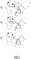
US 2010/0148846 A1 décrit un tel procédé mis en œuvre dans un circuit 10 représenté schématiquement sur lesfigures 1A à 1C . - Le circuit 10 comporte un transistor IGBT 16 dont la grille 22 est connectée :
- via un premier interrupteur S1D1, à un premier point 14 porté à un potentiel tel que la différence de potentiels entre ce premier point et un point de masse 18 corresponde à la première tension, VD;
- via un second interrupteur S3, à un second point 12 porté à un potentiel tel que la différence de potentiels entre ce premier point et le point de masse 18 corresponde à la seconde tension, VC ; et,
- via un troisième interrupteur S2, au point de masse 18.
- Par ailleurs, l'émetteur 26 du transistor 16 est connecté au point de masse 18 et le collecteur 24 du transistor 16 à une charge (non représentée sur les figures).
- Dans l'étape d'amorçage du basculement du transistor dans l'état passant (« ON »), représentée à la
figure 1A , les interrupteurs S3 et S2 sont ouverts, tandis que l'interrupteur S1D1 est fermé, de sorte que la tension VGE entre l'émetteur 26 et la grille 22 soit égale à la première tension VD. - Dans l'étape de maintien du transistor dans l'état passant (« ON »), représentée à la
figure 1B , les interrupteurs S1D1 et S2 sont ouverts, tandis que l'interrupteur S3 est fermé, de sorte que la tension VGE entre l'émetteur 26 et la grille 22 soit égale à la seconde tension VC. - Dans une étape de basculement du transistor dans l'état bloquant (« OFF »), représentée à la
figure 1C , les interrupteurs S1D1 et S3 sont ouverts, tandis que l'interrupteur S2 est fermé, de sorte que la tension VGE entre l'émetteur 26 et la grille 22 soit nulle. - La
figure 2 résume ces différentes étapes de pilotage du transistor 16 en représentant la tension VGE au cours du temps. On observe sur lafigure 2 que pour établir l'état passant, la première tension est d'abord appliquée sur la grille du transistor 16, pendant une période, dite d'amorçage, qui est courte devant la période totale durant laquelle le transistor est maintenu dans l'état passant. En d'autres termes, la période durant laquelle la première tension est appliquée sur la grille du transistor 16 est courte devant la période pendant laquelle la seconde tension est appliquée sur la grille du transistor 16. Pour établir l'état bloquant du transistor 16, on observe sur lafigure 2 que la tension VGE est annulée. - Cette solution est avantageuse mais est sensible aux perturbations, notamment les perturbations risquant de conduire au basculement du composant de puissance inopinément de l'état bloquant à l'état passant.
- Par ailleurs, le document
EP 0 369 448 A2 ou le documentDE 11 2016 006141 prévoit que pour basculer un transistor de puissance dans l'état passant, les interrupteurs de son circuit de contrôle sont commandés pour appliquer une première tension entre sa grille et son émetteur ; et que pour basculer ce même transistor dans l'état bloquant, les interrupteurs sont commandés pour appliquer une seconde tension entre sa grille et son émetteur, la première tension étant strictement positive et seconde tensions étant strictement négative. - Le but de la présente invention est de résoudre ce problème.
- Pour cela, l'invention a pour objet un procédé de pilotage d'un composant de puissance à grille isolé du type transistor, un circuit de pilotage d'un composant de puissance à grille isolé du type transistor et un dispositif de puissance selon les revendications annexées.
- L'invention et ses avantages seront mieux compris à la lecture de la description détaillée qui va suivre d'un mode de réalisation particulier, donné uniquement à titre d'exemple non limitatif, cette description étant faite en se référant aux dessins annexés sur lesquels :
- [
Fig 1 ] Lesfigures 1A à 1C représentent différentes étapes d'un procédé de pilotage d'un transistor selon l'état de la technique ; - [
Fig 2 ] lafigure 2 est un graphe temporel représentant l'évolution de la tension entre la grille et l'émetteur du transistor au cours de la mise en œuvre du procédé desfigures 1A à 1C ; - [
Fig 3 ] Lesfigures 3A à 3C représentent différentes étapes d'un procédé de pilotage d'un transistor selon l'invention ; et, - [
Fig 4 ] lafigure 4 est un graphe temporel représentant l'évolution de la tension entre la grille et l'émetteur du transistor au cours de la mise en œuvre du procédé desfigures 3A à 3C - Le circuit 110, représenté à la
figure 3 , comporte un transistor 116 en tant que composant de puissance à grille isolée. Il s'agit de préférence d'un transistor du type MOSFET, mais il pourrait en variante s'agir de tout type de transistor à grille isolée et notamment d'un transistor du type IGBT (les noms des bornes du transistor - grille, drain, source - seraient alors différents, au moins pour certaines des bornes du transistor, dans le texte ci-dessous mais le fonctionnement serait analogue). - Le transistor 116 comporte une grille 122, qui est connectée :
- via un premier interrupteur TrON, à un premier point 114 porté à un premier potentiel V1 (par exemple égal à +15 V) tel que la différence de potentiels entre ce premier point et un point de référence 113 corresponde à une première tension VD positive et supérieure à un seuil de conduction du transistor 116 au-delà duquel se dernier devient passant (seuil de conduction qui est une caractéristique prédéfinie du transistor 116) ; et,
- via un second interrupteur TrOFF, à un second point 112 porté à un second potentiel V2 (par exemple égal à -5 V) tel que la différence de potentiels entre le premier point et ce second point corresponde à une seconde tension VC positive et supérieure à la première tension VD.
- Par ailleurs, la source 126 du transistor 116 est connectée :
- via un troisième interrupteur Tr1, au point de référence 113 porté à un troisième potentiel V3 (par exemple égal à +0V) ; et,
- via un quatrième interrupteur Tr2, au second point 112.
- Enfin, le drain 124 du transistor 116 est relié à une charge (non représentée sur les figures).
- Dans une étape, représentée à la
figure 3A , d'amorçage du basculement du transistor 116 dans l'état passant (« ON »), c'est-à-dire de commande du transistor de l'état boquant/bloqué vers l'état passant, les interrupteurs TrOFF et Tr2 sont ouverts, tandis que les interrupteurs TrON et Tr1 sont fermés, de sorte que la source 126 soit au potentiel du point de référence 113 et la grille 122 au potentiel du premier point 114. La tension VGS entre la source et la grille est alors égale à la première tension VD, VD=V1-V3 (égale à +15V selon les exemples numériques précédents). - Dans une étape, représentée à la
figure 3B , de basculement définitif du transistor 116 dans l'état passant (« ON »), c'est-à-dire de maintien du transistor 116 dans l'état passant, les interrupteurs TrOFF et Tr1 sont ouverts, tandis que les interrupteurs TrON et Tr2 sont fermés, de sorte que la source 126 soit au potentiel du second point 112 et la grille 122 au potentiel du premier point 114. La tension VGE entre la source et la grille est alors égale à la seconde tension VC, VC=V1-V2 (égale à +20V selon les exemples numériques précédents). - Enfin, dans une étape, représentée à la
figure 3C , de basculement du transistor 116 dans l'état bloquant (« OFF »), c'est-à-dire de commande du transistor de l'état passant vers l'état boquant/bloqué, les interrupteurs TrON et Tr2 sont ouverts, tandis que les interrupteurs TrOFF et Tr1 sont fermés, de sorte que la source 126 soit au potentiel du point de référence 113 et la grille 122 au potentiel du second point 112. La tension VGE entre la source et la grille est alors égale à une troisième tension VOFF, qui est une tension négative correspondant à la différence entre la première tension VD et la seconde tension VC : VOFF= VD-VC=V2-V3 (égale à -5V selon les exemples numériques précédents). - La
figure 4 résume ces différentes étapes de pilotage du transistor 116 en représentant la tension VGS au cours du temps : la première tension VD est appliquée pendant une période d'amorçage courte, avant l'application de la seconde tension VC, pour établir l'état passant ; puis la tension VGS est fixée à la troisième tension VOFF pour établir l'état bloquant. - Le procédé selon l'invention consiste donc à basculer le composant de puissance dans l'état passant en deux étapes successives, un amorçage du basculement avec une tension intermédiaire, avant l'application d'une tension finale plus élevée. Le procédé selon l'invention consiste également à basculer le composant de puissance dans l'état bloquant par application d'une tension négative.
- En variante, le basculement dans l'état bloquant pourrait également se faire en deux étapes successives. Dans ce cas, l'établissement de l'état bloquant consistant à :
- amorcer l'état bloquant par application d'une première tension de blocage, ladite première tension de blocage étant inférieure au seuil de conduction du composant de puissance, supérieure à la troisième tension VOFF et appliquée pendant une durée d'amorçage du blocage (qui peut être choisie d'une durée différente de la durée d'amorçage de l'état passant) ; puis,
- maintenir l'état bloquant par application de la troisième tension VOFF.
- Pour l'établissement dans l'état passant, l'amorçage a pour effet d'améliorer la robustesse en cas de circulation d'un courant important entre le collecteur et l'émetteur du transistor 116, courant causé par un court-circuit dans le dispositif intégrant le circuit 110. Si aucun court-circuit n'est détecté, alors, dans un second temps, la tension finale, plus élevée, est appliquée pour réduire les pertes par conduction à l'intérieur du transistor 116 dans l'état passant.
- En effet, pour réduire les pertes par conduction dans les composants de puissance à grille isolée placés dans l'état passant, on doit appliquer une tension sur la grille la plus élevée possible. L'inconvénient est que plus cette tension est élevée moins le composant est robuste aux courants de court-circuit. En limitant les pertes, on dégrade donc la qualité de la protection aux courts-circuits.
- Ainsi pour un transistor MOSFET en technologie SiC, il est courant de devoir appliquer 20V de tension sur la grille (au lieu de 15V pour les composants Si (silicium) conventionnels) pour atteindre le niveau réduit de pertes caractérisant ce type de composants. La conséquence est de réduire la durée d'un court-circuit supportable par le transistor à environ 2µs. Le risque de dégradation du composant par un courant de court-circuit est par conséquent accru.
- Le procédé selon l'invention permet donc de garder les pertes par conduction à un niveau faible, en utilisant une seconde tension élevée, tout en augmentant la robustesse au court-circuit en initiant l'état passant avec une première tension plus faible. C'est cette première tension qui sera en jeu en cas de circulation à travers le composant d'un courant important de court-circuit.
- Par exemple, dans un dispositif du type allumeur intégrant le circuit 110, lorsqu'un court-circuit est présent au moment où le composant de puissance est basculé dans l'état passant, le système de détection/protection contre les courts-circuits du dispositif détecte la présence du court-circuit et commande le blocage du composant de puissance et le maintien dans l'état passant par application d'un second niveau de tension n'est pas exécuté. La durée d'amorçage doit donc être choisie de manière à permettre à ce système de détection/protection de jouer son rôle. La tension d'amorçage est choisie pour que la puissance dissipée pendant la période d'amorçage soit compatible des caractéristiques de résistance aux courts-circuits du composant de puissance utilisé.
- Pour le basculement dans l'état bloquant, que la tension VOFF soit négative a pour effet de sécuriser l'état du composant de puissance en l'immunisant contre les perturbations, notamment les perturbations risquant de conduire au basculement du composant de puissance dans l'état passant.
- Ceci est plus particulièrement intéressant pour des composants de puissance à commutation rapide utilisés dans des applications de forte puissance, comme par exemple les transistors du type MOSFET, en particulier ceux en technologie SiC.
- Il est à noter que les
figures 3 représentent un mode de réalisation du circuit selon l'invention à un niveau fonctionnel. L'homme du métier sait comment élaborer un circuit physique correspondant à ce circuit fonctionnel, notamment en sélectionnant et agençant des composants électroniques de manière à définir les potentiels des premier point, second point et point de référence, ainsi que pour réaliser les interrupteurs et les moyens pour en commander l'ouverture et la fermeture.
Claims (7)
- Procédé de pilotage d'un composant de puissance à grille isolée du type transistor (116) propre à être commandé entre un état passant et un état bloquant, du type comportant les étapes consistant à :- amorcer l'état passant par application, pendant une durée d'amorçage, d'une première tension (VD), ladite première tension étant une tension positive, supérieure à un seuil de conduction du composant de puissance ; puis,- maintenir l'état passant par application d'une seconde tension (VC), ladite seconde tension étant une tension positive, supérieure à la première tension,- établir l'état bloquant en appliquant une troisième tension (VOFF), ladite troisième tension étant strictement négative,caractérisé en ce que, une grille (122) du composant de puissance (116) étant connectée:- via un premier interrupteur (TrON), à un premier point (114) porté à un premier potentiel tel que la différence de potentiels entre le premier point et un point de référence (113) corresponde à la première tension (VD),et une source (126) du composant de puissance étant connectée:- via un troisième interrupteur (Tr1), au point de référence (113) porté à un troisième potentiel ; et,- via un quatrième interrupteur (Tr2), à un deuxième point (112) porté à un deuxième potentiel tel que la différence de potentiels entre le premier point et le deuxième point corresponde à la seconde tension (VC),lors de l'étape d'amorçage, les premier et troisième interrupteurs sont commandés dans l'état fermé tandis que le quatrième interrupteur est commandé dans l'état ouvert,
et lors de l'étape de maintien dans l'état passant, les premier et quatrième interrupteurs sont commandés dans l'état fermé tandis que le troisième interrupteur est commandé dans l'état ouvert. - Procédé selon la revendication 1, dans lequel le transistor est du type MOSFET, en particulier du type MOSFET en technologie SiC.
- Procédé selon la revendication 1 ou la revendication 2, dans lequel la grille (122) du composant de puissance (116) est connectée via un deuxième interrupteur (TrOFF), à un troisième point (112) porté à un quatrième potentiel tel que la différence de potentiels entre le troisième point et le point de référence est égale à la troisième tension,
et dans lequel lors de l'étape d'établissement de l'état bloquant, le deuxième interrupteur et le troisième interrupteur sont commandés dans l'état fermé, tandis que les premier et quatrième interrupteurs sont commandés dans l'état ouvert. - Procédé selon la revendication 3, dans lequel le deuxième potentiel et le quatrième potentiel sont égaux, les deuxième et troisième points étant confondus, et dans lequel, lors des étapes d'amorçage et de maintien dans l'état passant, le deuxième interrupteur est commandé dans l'état ouvert.
- Circuit de pilotage d'un composant de puissance à grille isolée du type transistor (116) pour la mise en œuvre d'un procédé de pilotage conforme à l'une quelconque des revendications précédentes, ledit circuit étant caractérisé en ce qu'il comprend un premier, un troisième et un quatrième interrupteur,
le premier interrupteur étant propre à connecter une grille (122) du composant de puissance (116) à un premier point (114) porté à un premier potentiel tel que la différence de potentiels entre le premier point et un point de référence (113) du circuit de pilotage corresponde à une première tension (VD) ;
le troisième interrupteur (Tr1) étant propre à connecter une source (126) du composant de puissance au point de référence (113) porté à un troisième potentiel ; et,
le quatrième interrupteur (Tr2) étant propre à connecter la source (126) à un deuxième point (112), porté à un deuxième potentiel tel que la différence de potentiels entre le premier point et le deuxième point corresponde à une seconde tension (VC). - Circuit de pilotage selon la revendication 5, ledit circuit étant caractérisé en ce qu'il comprend un deuxième interrupteur (TrOFF), le deuxième interrupteur étant propre à connecter la grille (122) du composant de puissance (116) à un troisième point (112) porté à un quatrième potentiel tel que la différence de potentiels entre le troisième point et le point de référence est égale à la troisième tension.
- Dispositif de puissance, caractérisé en ce qu'il comporte au moins un composant de puissance à grille isolée du type transistor (116) piloté par un circuit de pilotage conforme à l'une quelconque des revendications 5 à 6.
Applications Claiming Priority (1)
| Application Number | Priority Date | Filing Date | Title |
|---|---|---|---|
| FR1872228A FR3089369B1 (fr) | 2018-12-03 | 2018-12-03 | Procédé de pilotage d’un composant à grille isolée et circuit de pilotage correspondant |
Publications (2)
| Publication Number | Publication Date |
|---|---|
| EP3664293A1 true EP3664293A1 (fr) | 2020-06-10 |
| EP3664293B1 EP3664293B1 (fr) | 2021-03-24 |
Family
ID=66286447
Family Applications (1)
| Application Number | Title | Priority Date | Filing Date |
|---|---|---|---|
| EP19212899.9A Active EP3664293B1 (fr) | 2018-12-03 | 2019-12-02 | Procédé de pilotage d'un composant à grille isolée et circuit de pilotage correspondant |
Country Status (2)
| Country | Link |
|---|---|
| EP (1) | EP3664293B1 (fr) |
| FR (1) | FR3089369B1 (fr) |
Citations (3)
| Publication number | Priority date | Publication date | Assignee | Title |
|---|---|---|---|---|
| EP0369448A2 (fr) | 1988-11-16 | 1990-05-23 | Fuji Electric Co., Ltd. | Circuit d'attaque utilisable pour dispositif semi-conducteur commandé en tension |
| US20100148846A1 (en) | 2007-09-12 | 2010-06-17 | Mitsubishi Electric Corporation | Gate drive circuit |
| DE112016006141T5 (de) | 2016-06-24 | 2018-09-13 | Hitachi, Ltd. | Gate-Treiberschaltung, Stromwandler und Schienenfahrzeug |
-
2018
- 2018-12-03 FR FR1872228A patent/FR3089369B1/fr not_active Expired - Fee Related
-
2019
- 2019-12-02 EP EP19212899.9A patent/EP3664293B1/fr active Active
Patent Citations (3)
| Publication number | Priority date | Publication date | Assignee | Title |
|---|---|---|---|---|
| EP0369448A2 (fr) | 1988-11-16 | 1990-05-23 | Fuji Electric Co., Ltd. | Circuit d'attaque utilisable pour dispositif semi-conducteur commandé en tension |
| US20100148846A1 (en) | 2007-09-12 | 2010-06-17 | Mitsubishi Electric Corporation | Gate drive circuit |
| DE112016006141T5 (de) | 2016-06-24 | 2018-09-13 | Hitachi, Ltd. | Gate-Treiberschaltung, Stromwandler und Schienenfahrzeug |
Also Published As
| Publication number | Publication date |
|---|---|
| EP3664293B1 (fr) | 2021-03-24 |
| FR3089369B1 (fr) | 2021-07-09 |
| FR3089369A1 (fr) | 2020-06-05 |
Similar Documents
| Publication | Publication Date | Title |
|---|---|---|
| EP2276173B1 (fr) | Dispositif de commande d'un transistor de puissance | |
| FR3107627A1 (fr) | Circuit de contrôle d'une photodiode SPAD | |
| FR2678769A1 (fr) | Systeme pour interrompre rapidement, sans formation d'arc, un courant alternatif fourni a une charge. | |
| FR3004019A1 (fr) | Composant de protection contre des surtensions | |
| EP0520858B1 (fr) | Miroir de courant fonctionnant sous faible tension | |
| EP3545622A1 (fr) | Dispositif de commutation d'un circuit de puissance presentant un circuit passif de protection | |
| EP3070798B1 (fr) | Dispositif de protection contre des surtensions | |
| FR2547133A1 (fr) | Circuit destine a prevenir une dissipation excessive d'energie dans les dispositifs commutateurs de puissance | |
| EP3545621B1 (fr) | Dispositif de commutation d'un circuit de puissance | |
| EP3664293B1 (fr) | Procédé de pilotage d'un composant à grille isolée et circuit de pilotage correspondant | |
| EP3806162A1 (fr) | Extinction d'une spad | |
| FR3023060A1 (fr) | Composant de protection contre des surtensions | |
| FR3013920A1 (fr) | Dispositif electronique de commutation avec reduction des courants de fuite et procede de commande correspondant | |
| EP2164157A2 (fr) | Circuit de commande d'un transistor IGBT, et circuit de communication électronique comprenant un transistor IGBT et un tel circuit de commande | |
| WO2022117481A1 (fr) | Convertisseur de puissance | |
| WO2004075390A2 (fr) | Circuit de commande d’un moteur electrique a courant continu et systeme d’essuyage utilisant un tel circuit | |
| EP0180487A1 (fr) | Circuit de puissance et dispositif de déclenchement le comportant | |
| EP2293443B1 (fr) | Module électronique de commande pour transistor JFET | |
| EP3244536A1 (fr) | Circuit de limitation de tension, système d'interrupteur et convertisseur électrique | |
| EP4239885B1 (fr) | Pilote pour transistor a grille isolee avec circuit de compensation des temps de retard | |
| EP4118670B1 (fr) | Dispositif d'interrupteur hybride et de commande | |
| EP2783192B1 (fr) | Circuit de détection avec un module de réduction du bruit | |
| WO2001091295A1 (fr) | Thyristor dual, thyristor diode dual, composant formant thyristor, composant formant thyristor diode, convertisseur et interrupteur | |
| FR3083933A1 (fr) | Procede de reduction des perturbations electromagnetiques produites lors de la mise a l'etat passant d'un transistor | |
| EP1196994B1 (fr) | Procede de protection des semi-conducteurs de puissance d'un convertisseur de puissance et convertisseur mettant en oeuvre ce procede |
Legal Events
| Date | Code | Title | Description |
|---|---|---|---|
| PUAI | Public reference made under article 153(3) epc to a published international application that has entered the european phase |
Free format text: ORIGINAL CODE: 0009012 |
|
| STAA | Information on the status of an ep patent application or granted ep patent |
Free format text: STATUS: THE APPLICATION HAS BEEN PUBLISHED |
|
| STAA | Information on the status of an ep patent application or granted ep patent |
Free format text: STATUS: REQUEST FOR EXAMINATION WAS MADE |
|
| AK | Designated contracting states |
Kind code of ref document: A1 Designated state(s): AL AT BE BG CH CY CZ DE DK EE ES FI FR GB GR HR HU IE IS IT LI LT LU LV MC MK MT NL NO PL PT RO RS SE SI SK SM TR |
|
| AX | Request for extension of the european patent |
Extension state: BA ME |
|
| 17P | Request for examination filed |
Effective date: 20200526 |
|
| RBV | Designated contracting states (corrected) |
Designated state(s): AL AT BE BG CH CY CZ DE DK EE ES FI FR GB GR HR HU IE IS IT LI LT LU LV MC MK MT NL NO PL PT RO RS SE SI SK SM TR |
|
| GRAP | Despatch of communication of intention to grant a patent |
Free format text: ORIGINAL CODE: EPIDOSNIGR1 |
|
| STAA | Information on the status of an ep patent application or granted ep patent |
Free format text: STATUS: GRANT OF PATENT IS INTENDED |
|
| RIC1 | Information provided on ipc code assigned before grant |
Ipc: H03K 17/082 20060101ALI20200922BHEP Ipc: H03K 17/06 20060101ALI20200922BHEP Ipc: H03K 17/0812 20060101AFI20200922BHEP |
|
| INTG | Intention to grant announced |
Effective date: 20201015 |
|
| RAP1 | Party data changed (applicant data changed or rights of an application transferred) |
Owner name: ALSTOM TRANSPORT TECHNOLOGIES |
|
| GRAS | Grant fee paid |
Free format text: ORIGINAL CODE: EPIDOSNIGR3 |
|
| GRAA | (expected) grant |
Free format text: ORIGINAL CODE: 0009210 |
|
| STAA | Information on the status of an ep patent application or granted ep patent |
Free format text: STATUS: THE PATENT HAS BEEN GRANTED |
|
| AK | Designated contracting states |
Kind code of ref document: B1 Designated state(s): AL AT BE BG CH CY CZ DE DK EE ES FI FR GB GR HR HU IE IS IT LI LT LU LV MC MK MT NL NO PL PT RO RS SE SI SK SM TR |
|
| REG | Reference to a national code |
Ref country code: GB Ref legal event code: FG4D Free format text: NOT ENGLISH |
|
| REG | Reference to a national code |
Ref country code: CH Ref legal event code: EP |
|
| REG | Reference to a national code |
Ref country code: IE Ref legal event code: FG4D Free format text: LANGUAGE OF EP DOCUMENT: FRENCH |
|
| REG | Reference to a national code |
Ref country code: DE Ref legal event code: R096 Ref document number: 602019003437 Country of ref document: DE Ref country code: AT Ref legal event code: REF Ref document number: 1375547 Country of ref document: AT Kind code of ref document: T Effective date: 20210415 |
|
| REG | Reference to a national code |
Ref country code: CH Ref legal event code: NV Representative=s name: NOVAGRAAF INTERNATIONAL SA, CH |
|
| REG | Reference to a national code |
Ref country code: LT Ref legal event code: MG9D |
|
| PG25 | Lapsed in a contracting state [announced via postgrant information from national office to epo] |
Ref country code: HR Free format text: LAPSE BECAUSE OF FAILURE TO SUBMIT A TRANSLATION OF THE DESCRIPTION OR TO PAY THE FEE WITHIN THE PRESCRIBED TIME-LIMIT Effective date: 20210324 Ref country code: BG Free format text: LAPSE BECAUSE OF FAILURE TO SUBMIT A TRANSLATION OF THE DESCRIPTION OR TO PAY THE FEE WITHIN THE PRESCRIBED TIME-LIMIT Effective date: 20210624 Ref country code: FI Free format text: LAPSE BECAUSE OF FAILURE TO SUBMIT A TRANSLATION OF THE DESCRIPTION OR TO PAY THE FEE WITHIN THE PRESCRIBED TIME-LIMIT Effective date: 20210324 Ref country code: GR Free format text: LAPSE BECAUSE OF FAILURE TO SUBMIT A TRANSLATION OF THE DESCRIPTION OR TO PAY THE FEE WITHIN THE PRESCRIBED TIME-LIMIT Effective date: 20210625 Ref country code: NO Free format text: LAPSE BECAUSE OF FAILURE TO SUBMIT A TRANSLATION OF THE DESCRIPTION OR TO PAY THE FEE WITHIN THE PRESCRIBED TIME-LIMIT Effective date: 20210624 |
|
| PG25 | Lapsed in a contracting state [announced via postgrant information from national office to epo] |
Ref country code: LV Free format text: LAPSE BECAUSE OF FAILURE TO SUBMIT A TRANSLATION OF THE DESCRIPTION OR TO PAY THE FEE WITHIN THE PRESCRIBED TIME-LIMIT Effective date: 20210324 Ref country code: RS Free format text: LAPSE BECAUSE OF FAILURE TO SUBMIT A TRANSLATION OF THE DESCRIPTION OR TO PAY THE FEE WITHIN THE PRESCRIBED TIME-LIMIT Effective date: 20210324 Ref country code: SE Free format text: LAPSE BECAUSE OF FAILURE TO SUBMIT A TRANSLATION OF THE DESCRIPTION OR TO PAY THE FEE WITHIN THE PRESCRIBED TIME-LIMIT Effective date: 20210324 |
|
| REG | Reference to a national code |
Ref country code: NL Ref legal event code: MP Effective date: 20210324 |
|
| REG | Reference to a national code |
Ref country code: AT Ref legal event code: MK05 Ref document number: 1375547 Country of ref document: AT Kind code of ref document: T Effective date: 20210324 |
|
| PG25 | Lapsed in a contracting state [announced via postgrant information from national office to epo] |
Ref country code: NL Free format text: LAPSE BECAUSE OF FAILURE TO SUBMIT A TRANSLATION OF THE DESCRIPTION OR TO PAY THE FEE WITHIN THE PRESCRIBED TIME-LIMIT Effective date: 20210324 |
|
| PG25 | Lapsed in a contracting state [announced via postgrant information from national office to epo] |
Ref country code: AT Free format text: LAPSE BECAUSE OF FAILURE TO SUBMIT A TRANSLATION OF THE DESCRIPTION OR TO PAY THE FEE WITHIN THE PRESCRIBED TIME-LIMIT Effective date: 20210324 Ref country code: SM Free format text: LAPSE BECAUSE OF FAILURE TO SUBMIT A TRANSLATION OF THE DESCRIPTION OR TO PAY THE FEE WITHIN THE PRESCRIBED TIME-LIMIT Effective date: 20210324 Ref country code: LT Free format text: LAPSE BECAUSE OF FAILURE TO SUBMIT A TRANSLATION OF THE DESCRIPTION OR TO PAY THE FEE WITHIN THE PRESCRIBED TIME-LIMIT Effective date: 20210324 Ref country code: CZ Free format text: LAPSE BECAUSE OF FAILURE TO SUBMIT A TRANSLATION OF THE DESCRIPTION OR TO PAY THE FEE WITHIN THE PRESCRIBED TIME-LIMIT Effective date: 20210324 Ref country code: EE Free format text: LAPSE BECAUSE OF FAILURE TO SUBMIT A TRANSLATION OF THE DESCRIPTION OR TO PAY THE FEE WITHIN THE PRESCRIBED TIME-LIMIT Effective date: 20210324 |
|
| PG25 | Lapsed in a contracting state [announced via postgrant information from national office to epo] |
Ref country code: IS Free format text: LAPSE BECAUSE OF FAILURE TO SUBMIT A TRANSLATION OF THE DESCRIPTION OR TO PAY THE FEE WITHIN THE PRESCRIBED TIME-LIMIT Effective date: 20210724 Ref country code: PL Free format text: LAPSE BECAUSE OF FAILURE TO SUBMIT A TRANSLATION OF THE DESCRIPTION OR TO PAY THE FEE WITHIN THE PRESCRIBED TIME-LIMIT Effective date: 20210324 Ref country code: SK Free format text: LAPSE BECAUSE OF FAILURE TO SUBMIT A TRANSLATION OF THE DESCRIPTION OR TO PAY THE FEE WITHIN THE PRESCRIBED TIME-LIMIT Effective date: 20210324 Ref country code: PT Free format text: LAPSE BECAUSE OF FAILURE TO SUBMIT A TRANSLATION OF THE DESCRIPTION OR TO PAY THE FEE WITHIN THE PRESCRIBED TIME-LIMIT Effective date: 20210726 Ref country code: RO Free format text: LAPSE BECAUSE OF FAILURE TO SUBMIT A TRANSLATION OF THE DESCRIPTION OR TO PAY THE FEE WITHIN THE PRESCRIBED TIME-LIMIT Effective date: 20210324 |
|
| REG | Reference to a national code |
Ref country code: DE Ref legal event code: R097 Ref document number: 602019003437 Country of ref document: DE |
|
| PG25 | Lapsed in a contracting state [announced via postgrant information from national office to epo] |
Ref country code: ES Free format text: LAPSE BECAUSE OF FAILURE TO SUBMIT A TRANSLATION OF THE DESCRIPTION OR TO PAY THE FEE WITHIN THE PRESCRIBED TIME-LIMIT Effective date: 20210324 Ref country code: AL Free format text: LAPSE BECAUSE OF FAILURE TO SUBMIT A TRANSLATION OF THE DESCRIPTION OR TO PAY THE FEE WITHIN THE PRESCRIBED TIME-LIMIT Effective date: 20210324 Ref country code: DK Free format text: LAPSE BECAUSE OF FAILURE TO SUBMIT A TRANSLATION OF THE DESCRIPTION OR TO PAY THE FEE WITHIN THE PRESCRIBED TIME-LIMIT Effective date: 20210324 |
|
| PLBE | No opposition filed within time limit |
Free format text: ORIGINAL CODE: 0009261 |
|
| STAA | Information on the status of an ep patent application or granted ep patent |
Free format text: STATUS: NO OPPOSITION FILED WITHIN TIME LIMIT |
|
| 26N | No opposition filed |
Effective date: 20220104 |
|
| PG25 | Lapsed in a contracting state [announced via postgrant information from national office to epo] |
Ref country code: IS Free format text: LAPSE BECAUSE OF FAILURE TO SUBMIT A TRANSLATION OF THE DESCRIPTION OR TO PAY THE FEE WITHIN THE PRESCRIBED TIME-LIMIT Effective date: 20210724 |
|
| PG25 | Lapsed in a contracting state [announced via postgrant information from national office to epo] |
Ref country code: MC Free format text: LAPSE BECAUSE OF FAILURE TO SUBMIT A TRANSLATION OF THE DESCRIPTION OR TO PAY THE FEE WITHIN THE PRESCRIBED TIME-LIMIT Effective date: 20210324 |
|
| REG | Reference to a national code |
Ref country code: BE Ref legal event code: MM Effective date: 20211231 |
|
| PG25 | Lapsed in a contracting state [announced via postgrant information from national office to epo] |
Ref country code: LU Free format text: LAPSE BECAUSE OF NON-PAYMENT OF DUE FEES Effective date: 20211202 Ref country code: IE Free format text: LAPSE BECAUSE OF NON-PAYMENT OF DUE FEES Effective date: 20211202 |
|
| PG25 | Lapsed in a contracting state [announced via postgrant information from national office to epo] |
Ref country code: BE Free format text: LAPSE BECAUSE OF NON-PAYMENT OF DUE FEES Effective date: 20211231 |
|
| PG25 | Lapsed in a contracting state [announced via postgrant information from national office to epo] |
Ref country code: CY Free format text: LAPSE BECAUSE OF FAILURE TO SUBMIT A TRANSLATION OF THE DESCRIPTION OR TO PAY THE FEE WITHIN THE PRESCRIBED TIME-LIMIT Effective date: 20210324 |
|
| PG25 | Lapsed in a contracting state [announced via postgrant information from national office to epo] |
Ref country code: HU Free format text: LAPSE BECAUSE OF FAILURE TO SUBMIT A TRANSLATION OF THE DESCRIPTION OR TO PAY THE FEE WITHIN THE PRESCRIBED TIME-LIMIT; INVALID AB INITIO Effective date: 20191202 |
|
| P01 | Opt-out of the competence of the unified patent court (upc) registered |
Effective date: 20230823 |
|
| PG25 | Lapsed in a contracting state [announced via postgrant information from national office to epo] |
Ref country code: SI Free format text: LAPSE BECAUSE OF FAILURE TO SUBMIT A TRANSLATION OF THE DESCRIPTION OR TO PAY THE FEE WITHIN THE PRESCRIBED TIME-LIMIT Effective date: 20210324 |
|
| PG25 | Lapsed in a contracting state [announced via postgrant information from national office to epo] |
Ref country code: MK Free format text: LAPSE BECAUSE OF FAILURE TO SUBMIT A TRANSLATION OF THE DESCRIPTION OR TO PAY THE FEE WITHIN THE PRESCRIBED TIME-LIMIT Effective date: 20210324 |
|
| PG25 | Lapsed in a contracting state [announced via postgrant information from national office to epo] |
Ref country code: TR Free format text: LAPSE BECAUSE OF FAILURE TO SUBMIT A TRANSLATION OF THE DESCRIPTION OR TO PAY THE FEE WITHIN THE PRESCRIBED TIME-LIMIT Effective date: 20210324 |
|
| PG25 | Lapsed in a contracting state [announced via postgrant information from national office to epo] |
Ref country code: MT Free format text: LAPSE BECAUSE OF FAILURE TO SUBMIT A TRANSLATION OF THE DESCRIPTION OR TO PAY THE FEE WITHIN THE PRESCRIBED TIME-LIMIT Effective date: 20210324 |
|
| REG | Reference to a national code |
Ref country code: GB Ref legal event code: 732E Free format text: REGISTERED BETWEEN 20250213 AND 20250219 |
|
| REG | Reference to a national code |
Ref country code: CH Ref legal event code: U11 Free format text: ST27 STATUS EVENT CODE: U-0-0-U10-U11 (AS PROVIDED BY THE NATIONAL OFFICE) Effective date: 20260101 |
|
| PGFP | Annual fee paid to national office [announced via postgrant information from national office to epo] |
Ref country code: DE Payment date: 20251211 Year of fee payment: 7 |
|
| PGFP | Annual fee paid to national office [announced via postgrant information from national office to epo] |
Ref country code: GB Payment date: 20251219 Year of fee payment: 7 |
|
| PGFP | Annual fee paid to national office [announced via postgrant information from national office to epo] |
Ref country code: IT Payment date: 20251223 Year of fee payment: 7 |
|
| PGFP | Annual fee paid to national office [announced via postgrant information from national office to epo] |
Ref country code: FR Payment date: 20251229 Year of fee payment: 7 |
|
| PGFP | Annual fee paid to national office [announced via postgrant information from national office to epo] |
Ref country code: CH Payment date: 20260101 Year of fee payment: 7 |