EP3664175A1 - Package structure and fabrication method therefor, and display device - Google Patents
Package structure and fabrication method therefor, and display device Download PDFInfo
- Publication number
- EP3664175A1 EP3664175A1 EP18841614.3A EP18841614A EP3664175A1 EP 3664175 A1 EP3664175 A1 EP 3664175A1 EP 18841614 A EP18841614 A EP 18841614A EP 3664175 A1 EP3664175 A1 EP 3664175A1
- Authority
- EP
- European Patent Office
- Prior art keywords
- film layer
- encapsulation
- encapsulation film
- layer
- forming
- Prior art date
- Legal status (The legal status is an assumption and is not a legal conclusion. Google has not performed a legal analysis and makes no representation as to the accuracy of the status listed.)
- Withdrawn
Links
Images

Classifications
-
- H—ELECTRICITY
- H10—SEMICONDUCTOR DEVICES; ELECTRIC SOLID-STATE DEVICES NOT OTHERWISE PROVIDED FOR
- H10K—ORGANIC ELECTRIC SOLID-STATE DEVICES
- H10K71/00—Manufacture or treatment specially adapted for the organic devices covered by this subclass
-
- B—PERFORMING OPERATIONS; TRANSPORTING
- B01—PHYSICAL OR CHEMICAL PROCESSES OR APPARATUS IN GENERAL
- B01D—SEPARATION
- B01D53/00—Separation of gases or vapours; Recovering vapours of volatile solvents from gases; Chemical or biological purification of waste gases, e.g. engine exhaust gases, smoke, fumes, flue gases, aerosols
- B01D53/26—Drying gases or vapours
- B01D53/261—Drying gases or vapours by adsorption
-
- B—PERFORMING OPERATIONS; TRANSPORTING
- B01—PHYSICAL OR CHEMICAL PROCESSES OR APPARATUS IN GENERAL
- B01D—SEPARATION
- B01D53/00—Separation of gases or vapours; Recovering vapours of volatile solvents from gases; Chemical or biological purification of waste gases, e.g. engine exhaust gases, smoke, fumes, flue gases, aerosols
- B01D53/26—Drying gases or vapours
- B01D53/28—Selection of materials for use as drying agents
-
- H—ELECTRICITY
- H10—SEMICONDUCTOR DEVICES; ELECTRIC SOLID-STATE DEVICES NOT OTHERWISE PROVIDED FOR
- H10K—ORGANIC ELECTRIC SOLID-STATE DEVICES
- H10K50/00—Organic light-emitting devices
- H10K50/80—Constructional details
- H10K50/84—Passivation; Containers; Encapsulations
- H10K50/841—Self-supporting sealing arrangements
-
- H—ELECTRICITY
- H10—SEMICONDUCTOR DEVICES; ELECTRIC SOLID-STATE DEVICES NOT OTHERWISE PROVIDED FOR
- H10K—ORGANIC ELECTRIC SOLID-STATE DEVICES
- H10K50/00—Organic light-emitting devices
- H10K50/80—Constructional details
- H10K50/84—Passivation; Containers; Encapsulations
- H10K50/842—Containers
- H10K50/8426—Peripheral sealing arrangements, e.g. adhesives, sealants
-
- H—ELECTRICITY
- H10—SEMICONDUCTOR DEVICES; ELECTRIC SOLID-STATE DEVICES NOT OTHERWISE PROVIDED FOR
- H10K—ORGANIC ELECTRIC SOLID-STATE DEVICES
- H10K50/00—Organic light-emitting devices
- H10K50/80—Constructional details
- H10K50/84—Passivation; Containers; Encapsulations
- H10K50/844—Encapsulations
-
- H—ELECTRICITY
- H10—SEMICONDUCTOR DEVICES; ELECTRIC SOLID-STATE DEVICES NOT OTHERWISE PROVIDED FOR
- H10K—ORGANIC ELECTRIC SOLID-STATE DEVICES
- H10K50/00—Organic light-emitting devices
- H10K50/80—Constructional details
- H10K50/84—Passivation; Containers; Encapsulations
- H10K50/844—Encapsulations
- H10K50/8445—Encapsulations multilayered coatings having a repetitive structure, e.g. having multiple organic-inorganic bilayers
-
- H—ELECTRICITY
- H10—SEMICONDUCTOR DEVICES; ELECTRIC SOLID-STATE DEVICES NOT OTHERWISE PROVIDED FOR
- H10K—ORGANIC ELECTRIC SOLID-STATE DEVICES
- H10K50/00—Organic light-emitting devices
- H10K50/80—Constructional details
- H10K50/84—Passivation; Containers; Encapsulations
- H10K50/846—Passivation; Containers; Encapsulations comprising getter material or desiccants
-
- H—ELECTRICITY
- H10—SEMICONDUCTOR DEVICES; ELECTRIC SOLID-STATE DEVICES NOT OTHERWISE PROVIDED FOR
- H10K—ORGANIC ELECTRIC SOLID-STATE DEVICES
- H10K59/00—Integrated devices, or assemblies of multiple devices, comprising at least one organic light-emitting element covered by group H10K50/00
- H10K59/10—OLED displays
- H10K59/12—Active-matrix OLED [AMOLED] displays
-
- H—ELECTRICITY
- H10—SEMICONDUCTOR DEVICES; ELECTRIC SOLID-STATE DEVICES NOT OTHERWISE PROVIDED FOR
- H10K—ORGANIC ELECTRIC SOLID-STATE DEVICES
- H10K59/00—Integrated devices, or assemblies of multiple devices, comprising at least one organic light-emitting element covered by group H10K50/00
- H10K59/80—Constructional details
- H10K59/87—Passivation; Containers; Encapsulations
- H10K59/873—Encapsulations
-
- H—ELECTRICITY
- H10—SEMICONDUCTOR DEVICES; ELECTRIC SOLID-STATE DEVICES NOT OTHERWISE PROVIDED FOR
- H10K—ORGANIC ELECTRIC SOLID-STATE DEVICES
- H10K59/00—Integrated devices, or assemblies of multiple devices, comprising at least one organic light-emitting element covered by group H10K50/00
- H10K59/80—Constructional details
- H10K59/87—Passivation; Containers; Encapsulations
- H10K59/873—Encapsulations
- H10K59/8731—Encapsulations multilayered coatings having a repetitive structure, e.g. having multiple organic-inorganic bilayers
-
- H—ELECTRICITY
- H10—SEMICONDUCTOR DEVICES; ELECTRIC SOLID-STATE DEVICES NOT OTHERWISE PROVIDED FOR
- H10K—ORGANIC ELECTRIC SOLID-STATE DEVICES
- H10K59/00—Integrated devices, or assemblies of multiple devices, comprising at least one organic light-emitting element covered by group H10K50/00
- H10K59/80—Constructional details
- H10K59/87—Passivation; Containers; Encapsulations
- H10K59/874—Passivation; Containers; Encapsulations including getter material or desiccant
-
- B—PERFORMING OPERATIONS; TRANSPORTING
- B01—PHYSICAL OR CHEMICAL PROCESSES OR APPARATUS IN GENERAL
- B01D—SEPARATION
- B01D2253/00—Adsorbents used in seperation treatment of gases and vapours
- B01D2253/10—Inorganic adsorbents
- B01D2253/112—Metals or metal compounds not provided for in B01D2253/104 or B01D2253/106
-
- B—PERFORMING OPERATIONS; TRANSPORTING
- B01—PHYSICAL OR CHEMICAL PROCESSES OR APPARATUS IN GENERAL
- B01D—SEPARATION
- B01D2253/00—Adsorbents used in seperation treatment of gases and vapours
- B01D2253/20—Organic adsorbents
- B01D2253/202—Polymeric adsorbents
-
- B—PERFORMING OPERATIONS; TRANSPORTING
- B01—PHYSICAL OR CHEMICAL PROCESSES OR APPARATUS IN GENERAL
- B01D—SEPARATION
- B01D2253/00—Adsorbents used in seperation treatment of gases and vapours
- B01D2253/25—Coated, impregnated or composite adsorbents
-
- B—PERFORMING OPERATIONS; TRANSPORTING
- B01—PHYSICAL OR CHEMICAL PROCESSES OR APPARATUS IN GENERAL
- B01D—SEPARATION
- B01D2253/00—Adsorbents used in seperation treatment of gases and vapours
- B01D2253/30—Physical properties of adsorbents
- B01D2253/302—Dimensions
- B01D2253/304—Linear dimensions, e.g. particle shape, diameter
-
- B—PERFORMING OPERATIONS; TRANSPORTING
- B01—PHYSICAL OR CHEMICAL PROCESSES OR APPARATUS IN GENERAL
- B01D—SEPARATION
- B01D2253/00—Adsorbents used in seperation treatment of gases and vapours
- B01D2253/30—Physical properties of adsorbents
- B01D2253/302—Dimensions
- B01D2253/308—Pore size
-
- H—ELECTRICITY
- H10—SEMICONDUCTOR DEVICES; ELECTRIC SOLID-STATE DEVICES NOT OTHERWISE PROVIDED FOR
- H10K—ORGANIC ELECTRIC SOLID-STATE DEVICES
- H10K2102/00—Constructional details relating to the organic devices covered by this subclass
- H10K2102/301—Details of OLEDs
- H10K2102/351—Thickness
Definitions
- both of an organic light emitting material layer and a cathode formed by an active metal are very sensitive to moisture and oxygen, and a small amount of moisture or oxygen intruding into the device can cause rapid decay and aging of the device, therefore the light emitting display device has high requirements for preventing moisture and oxygen. Therefore, the organic light emitting display device places high demands on packaging processes and conditions.
- the adsorption structure includes a plurality of pores, and the plurality of pores are uniformly distributed in the encapsulation film layer.
- a volume ratio of the pores in the encapsulation film layer per unit volume ranges from 10% to 40%.
- each of the pores is partially filled with an inert gas.
- the encapsulation film layer is made of an alkali metal halide composite material or an organic polymer resin material.
- the package structure includes an organic encapsulation layer and an inorganic encapsulation layer, wherein the organic encapsulation layer and the inorganic encapsulation layer are sequentially stacked on the encapsulation film layer.
- the package structure further includes an organic encapsulation layer and an inorganic encapsulation layer, wherein the organic encapsulation layer and the inorganic encapsulation layer are sequentially stacked on a side of the organic light emitting device away from the substrate, and the encapsulation film layer is interposed between the organic encapsulation layer and the inorganic encapsulation layer.
- the package structure includes more than one encapsulation film layer, more than one organic encapsulation layer and more than one inorganic encapsulation layer.
- An embodiment of the present disclosure provides a display device including the above package structure.
- An embodiment of the present disclosure provides a manufacturing method for a package structure, wherein the package structure includes a substrate, an organic light emitting device, and a first encapsulation film layer, the manufacturing method including: forming the organic light emitting device on the substrate; forming the first encapsulation film layer above the organic light emitting device to encapsulate the organic light emitting device onto the substrate, wherein an adsorption structure is formed in the first encapsulation film layer, and the adsorption structure is configured to absorb moisture and oxygen.
- forming the first encapsulation film layer includes: forming the first encapsulation film layer adopting an alkali metal halide composite material by using an evaporation method.
- forming the first encapsulation film layer includes: forming the first encapsulation film layer adopting an organic polymer resin material by using a printing method or a spin coating method.
- the adsorption structure includes a plurality of pores
- forming the first encapsulation film layer further includes: during the evaporation process, an inert gas is introduced into a material, which is to be evaporated to form the first encapsulation film layer, to form the pores in the first encapsulation film layer.
- a flow rate of the inert gas introduced into the material to be evaporated ranges from 1sccm to 10sccm, an evaporation ambient pressure is not less than 1.0E-5 Pa, and an evaporation rate ranges from 4 ⁇ /s to 5 ⁇ /s.
- the manufacturing method further includes sequentially forming a first inorganic encapsulation layer and a first organic encapsulation layer on the first encapsulation film layer.
- forming the second encapsulation film layer further includes: forming the second encapsulation film layer adopting an alkali metal halide composite material by using an evaporation method, wherein during the evaporation process, an inert gas is introduced into a material, which is to be evaporated to form the second encapsulation film layer by the evaporation method, to form pores in the second encapsulation film layer.
- An embodiment of the present disclosure provides a package structure, as shown in FIG. 1 , which includes a substrate 1 and an organic light emitting device 2 disposed on the substrate 1, and an encapsulation film layer 3 covering the organic light emitting device 2 and being configured to encapsulate the organic light emitting device 2 onto the substrate 1, wherein an adsorption structure is formed in the encapsulation film layer 3.
- the adsorption structure may specifically be a water-oxygen absorption structure 4, and the water-oxygen absorption structure 4 can absorb moisture and oxygen.
- the substrate 1 is a flexible substrate
- the package structure is a flexible structure.
- moisture and oxygen in the package structure can be absorbed, thereby avoiding the organic light emitting device 2 from being corroded and damaged by moisture and oxygen, thereby improving package quality for the organic light emitting device 2 and prolonging the lifetime of the organic light emitting device 2.
- a size of each of the pores ranges from 0.1 nm to 10 nm.
- the pore of this size can well absorb, accommodate and enclose moisture and oxygen inside the package structure, so as to avoid the organic light emitting device 2 from being corroded and damaged by moisture and oxygen.
- a volume ratio of the pores in the encapsulation film layer 3 per unit volume ranges from 10% to 40%.
- the volume ratio of the pores is favorable for sufficiently absorbing, accommodating and enclosing moisture and oxygen inside the package structure, so as to avoid the organic light emitting device 2 from being corroded and damaged by moisture and oxygen.
- a thickness of the encapsulation film layer 3 ranges from 50 nm to 70 nm.
- the thickness of the encapsulation film layer 3 can achieve sufficient absorption and enclosing of moisture and oxygen inside the package structure to avoid the organic light emitting device 2 from being corroded and damaged by moisture and oxygen.
- the pores are partially filled with an inert gas.
- the inert gas facilitates the formation of pores in the encapsulation film layer 3, and on the other hand, since the pores are partially filled with the inert gas, the moisture and oxygen can enter the remaining space of the pores, preventing the moisture and oxygen from contacting the organic light emitting device 2.
- the encapsulation film layer 3 is made of an alkali metal halide composite material. It should be noted that the encapsulation film layer 3 may also be made of an organic polymer resin material. The encapsulation film layer 3 made of each of the above materials is advantageous in forming pores therein. Among the above materials, the organic polymer resin material may be one or more of an aromatic polyamine resin material and a polyamide resin material.
- the package structure further includes an organic encapsulation layer 5 and an inorganic encapsulation layer 6, and the organic encapsulation layer 5 and the inorganic encapsulation layer 6 are sequentially stacked on the encapsulation film layer 3.
- the organic encapsulation layer 5 is made of a conventional organic material such as polyurethane, polyethylene or polyvinyl chloride
- the inorganic encapsulation layer 6 is made of a conventional inorganic material such as silicon nitride, silicon oxide or silicon oxynitride.
- the arrangement of the organic encapsulation layer 5 and the inorganic encapsulation layer 6 can further block the intrusion of the moisture and oxygen in the environment into the interior of the package structure, thereby avoiding the organic light emitting device 2 from being corroded and damaged by moisture and oxygen.
- organic encapsulation layer 5 and more than one inorganic encapsulation layer 6 may be provided, and organic encapsulation layers 5 and inorganic encapsulation layers 6 may be alternately stacked on the encapsulation film layer 3 to form a plurality of encapsulations for the organic light emitting device 2 to prevent the moisture and oxygen in the environment from entering the interior of the package structure.
- the present embodiment further provides a manufacturing method for a package structure, as shown in FIG. 3 , the manufacturing method includes forming an organic light emitting device on a substrate, forming an encapsulation film layer above the organic light emitting device to encapsulate the organic light emitting device onto the substrate while forming a water-oxygen absorption structure in the encapsulation film layer.
- the encapsulation film layer may be made of an alkali metal halide composite material by an evaporation method.
- the water-oxygen absorption structure includes a plurality of pores, and during the evaporation process, an inert gas is introduced into a material, which is to be evaporated to form the encapsulation film layer by the evaporation method, to form the pores in the encapsulation film layer.
- a flow rate of the inert gas introduced into the material to be evaporated is in a range from 1 sccm to 10 sccm.
- An evaporation ambient pressure is not less than 1.0E-5 Pa and an evaporation rate is in a range from 4 A/s to 5 A/s.
- a plurality of uniformly distributed pores can be formed in the encapsulation film layer, and the pores can sufficiently absorb, accommodate and enclose the moisture and oxygen inside the package structure to avoid the light emitting device from being corroded and damaged by the moisture and oxygen.
- the manufacturing method for the package structure further includes sequentially forming an organic encapsulation layer and an inorganic encapsulation layer on the encapsulation film layer.
- the organic encapsulation layer is formed by a conventional printing or spin coating method
- the inorganic encapsulation layer is formed by a conventional chemical vapor deposition method, and details thereof are not described herein.
- more than one encapsulation film layer 3, more than one organic encapsulation layer 5, and more than one inorganic encapsulation layer 6 may be provided.
- a manufacturing method for the above package structure is further provided.
- an organic encapsulation layer, an encapsulation film layer and an inorganic encapsulation layer are sequentially formed above the substrate.
- Specific manufacturing method of each film layer is the same as that in the above embodiment, and will not be described again.
- Advantageous effects of the embodiments in the present disclosure are as follows: in the package structure, by forming the water-oxygen absorption structure in the encapsulation film layer, moisture and oxygen in the package structure can be absorbed, thereby avoiding the organic light emitting device from being corroded and damaged by moisture and oxygen, thereby improving the package quality for the organic light emitting device and prolonging its lifetime.
- the package quality of the display device is improved, and the lifetime of the display device is prolonged.
- the display device provided by the present disclosure may be any product or component having a display function such as an OLED panel, an OLED TV, a display, a mobile phone, a navigator or the like.
Landscapes
- Chemical & Material Sciences (AREA)
- Engineering & Computer Science (AREA)
- Physics & Mathematics (AREA)
- Optics & Photonics (AREA)
- Inorganic Chemistry (AREA)
- Manufacturing & Machinery (AREA)
- Analytical Chemistry (AREA)
- General Chemical & Material Sciences (AREA)
- Oil, Petroleum & Natural Gas (AREA)
- Chemical Kinetics & Catalysis (AREA)
- Microelectronics & Electronic Packaging (AREA)
- Electroluminescent Light Sources (AREA)
Abstract
Description
- The present application claims priority to Chinese Patent Application No.
201710646937.X filed on August 1, 2017 - The present disclosure relates to the field of display technologies, and in particular, to a package structure and a manufacturing method for the same, and a display device.
- In a novel flexible organic light emitting display device (AMOLED), both of an organic light emitting material layer and a cathode formed by an active metal are very sensitive to moisture and oxygen, and a small amount of moisture or oxygen intruding into the device can cause rapid decay and aging of the device, therefore the light emitting display device has high requirements for preventing moisture and oxygen. Therefore, the organic light emitting display device places high demands on packaging processes and conditions.
- An embodiment of the present disclosure provides a package structure including: a substrate; an organic light emitting device disposed on the substrate; an encapsulation film layer disposed above the organic light emitting device, the encapsulation film layer encapsulating the organic light emitting device onto the substrate, wherein an adsorption structure is formed in the encapsulation film layer, and the adsorption structure is configured to absorb moisture and oxygen.
- In some implementations, the adsorption structure includes a plurality of pores, and the plurality of pores are uniformly distributed in the encapsulation film layer.
- In some implementations, each of the pores has a size ranging from 0.1nm to 10 nm.
- In some implementations, a volume ratio of the pores in the encapsulation film layer per unit volume ranges from 10% to 40%.
- In some implementations, the encapsulation film layer has a thickness ranging from 50 nm to 70 nm.
- In some implementations, each of the pores is partially filled with an inert gas.
- In some implementations, the encapsulation film layer is made of an alkali metal halide composite material or an organic polymer resin material.
- In some implementations, the package structure includes an organic encapsulation layer and an inorganic encapsulation layer, wherein the organic encapsulation layer and the inorganic encapsulation layer are sequentially stacked on the encapsulation film layer.
- In some implementations, the package structure further includes an organic encapsulation layer and an inorganic encapsulation layer, wherein the organic encapsulation layer and the inorganic encapsulation layer are sequentially stacked on a side of the organic light emitting device away from the substrate, and the encapsulation film layer is interposed between the organic encapsulation layer and the inorganic encapsulation layer.
- In some implementations, the package structure includes more than one encapsulation film layer, more than one organic encapsulation layer and more than one inorganic encapsulation layer.
- An embodiment of the present disclosure provides a display device including the above package structure.
- An embodiment of the present disclosure provides a manufacturing method for a package structure, wherein the package structure includes a substrate, an organic light emitting device, and a first encapsulation film layer, the manufacturing method including: forming the organic light emitting device on the substrate; forming the first encapsulation film layer above the organic light emitting device to encapsulate the organic light emitting device onto the substrate, wherein an adsorption structure is formed in the first encapsulation film layer, and the adsorption structure is configured to absorb moisture and oxygen.
- In some implementations, forming the first encapsulation film layer includes: forming the first encapsulation film layer adopting an alkali metal halide composite material by using an evaporation method.
- In some implementations, forming the first encapsulation film layer includes: forming the first encapsulation film layer adopting an organic polymer resin material by using a printing method or a spin coating method.
- In some implementations, the adsorption structure includes a plurality of pores, and forming the first encapsulation film layer further includes: during the evaporation process, an inert gas is introduced into a material, which is to be evaporated to form the first encapsulation film layer, to form the pores in the first encapsulation film layer.
- In some implementations, a flow rate of the inert gas introduced into the material to be evaporated ranges from 1sccm to 10sccm, an evaporation ambient pressure is not less than 1.0E-5 Pa, and an evaporation rate ranges from 4 Å/s to 5Å/s.
- In some implementations, the manufacturing method further includes sequentially forming a first inorganic encapsulation layer and a first organic encapsulation layer on the first encapsulation film layer.
- In some implementations, the manufacturing method further includes: before forming the first encapsulation film layer, forming a first inorganic encapsulation layer on the organic light emitting device to encapsulate the organic light emitting device onto the substrate; and after forming the first encapsulation film layer, forming a first organic encapsulation layer on the first encapsulation film layer, wherein forming the first encapsulation film layer further includes forming the first encapsulation film layer on the first inorganic encapsulation layer.
- In some implementations, the manufacturing method further includes: before forming the first encapsulation film layer, forming a first inorganic encapsulation layer above the organic light emitting device to encapsulate the organic light emitting device onto the substrate; after forming the first encapsulation film layer, forming a first organic encapsulation layer on the first encapsulation film layer; forming a second encapsulation film layer on the first organic encapsulation layer; and forming a second inorganic encapsulation film layer on the second encapsulation film layer, wherein forming the first encapsulation film layer further includes forming the first encapsulation film layer on the first inorganic encapsulation layer.
- In some implementations, forming the first encapsulation film layer further includes: forming the first encapsulation film layer adopting an alkali metal halide composite material by using an evaporation method, wherein during the evaporation process, an inert gas is introduced into a material, which is to be evaporated to form the first encapsulation film layer by the evaporation method, to form pores in the first encapsulation film layer.
- In some implementations, forming the second encapsulation film layer further includes: forming the second encapsulation film layer adopting an alkali metal halide composite material by using an evaporation method, wherein during the evaporation process, an inert gas is introduced into a material, which is to be evaporated to form the second encapsulation film layer by the evaporation method, to form pores in the second encapsulation film layer.
-
-
Fig. 1 is a cross-sectional view showing a configuration of a package structure according to an embodiment of the present disclosure; -
Fig. 2 is a cross-sectional view showing the configuration of a package structure according to another embodiment of the present disclosure; -
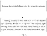
Fig. 3 is a flow chart of a manufacturing method for a package structure according to an embodiment of the present disclosure. - In order to enable a person skilled in the art to better understand the technical solutions of the present disclosure, a package structure and a manufacturing method for the same and a display device provided by the present disclosure are further described in detail below with reference to the accompanying drawings and specific embodiments.
- An embodiment of the present disclosure provides a package structure, as shown in
FIG. 1 , which includes a substrate 1 and an organiclight emitting device 2 disposed on the substrate 1, and anencapsulation film layer 3 covering the organiclight emitting device 2 and being configured to encapsulate the organiclight emitting device 2 onto the substrate 1, wherein an adsorption structure is formed in theencapsulation film layer 3. In the present embodiment, the adsorption structure may specifically be a water-oxygen absorption structure 4, and the water-oxygen absorption structure 4 can absorb moisture and oxygen. - According to an embodiment of the present disclosure, the substrate 1 is a flexible substrate, and the package structure is a flexible structure. By forming the water-oxygen absorption structure 4 in the
encapsulation film layer 3, moisture and oxygen in the package structure can be absorbed, thereby avoiding the organiclight emitting device 2 from being corroded and damaged by moisture and oxygen, thereby improving package quality for the organiclight emitting device 2 and prolonging the lifetime of the organiclight emitting device 2. - In the present embodiment, the water-oxygen absorption structure 4 includes a plurality of pores, and the plurality of pores are uniformly distributed in the
encapsulation film layer 3. The uniformly distributed pores in theencapsulation film layer 3 can absorb, accommodate and enclose moisture and oxygen in the package structure, thereby preventing moisture and oxygen from directly contacting the organiclight emitting device 2 to corrode or damage the organiclight emitting device 2, which in turn improves the package quality for the organiclight emitting device 2, while also prolonging lifetime of the organiclight emitting device 2. - In the present embodiment, a size of each of the pores ranges from 0.1 nm to 10 nm. The pore of this size can well absorb, accommodate and enclose moisture and oxygen inside the package structure, so as to avoid the organic
light emitting device 2 from being corroded and damaged by moisture and oxygen. - In the present embodiment, a volume ratio of the pores in the
encapsulation film layer 3 per unit volume ranges from 10% to 40%. The volume ratio of the pores is favorable for sufficiently absorbing, accommodating and enclosing moisture and oxygen inside the package structure, so as to avoid the organiclight emitting device 2 from being corroded and damaged by moisture and oxygen. - In the present embodiment, a thickness of the
encapsulation film layer 3 ranges from 50 nm to 70 nm. The thickness of theencapsulation film layer 3 can achieve sufficient absorption and enclosing of moisture and oxygen inside the package structure to avoid the organiclight emitting device 2 from being corroded and damaged by moisture and oxygen. - In the present embodiment, the pores are partially filled with an inert gas. On the one hand, the inert gas facilitates the formation of pores in the
encapsulation film layer 3, and on the other hand, since the pores are partially filled with the inert gas, the moisture and oxygen can enter the remaining space of the pores, preventing the moisture and oxygen from contacting the organiclight emitting device 2. In addition, since the inert gas itself does not react with the cathode or anode made of active metal and the organic light emitting material in the organiclight emitting device 2, therefore it can block the moisture and oxygen from the organiclight emitting device 2, blocking the moisture and oxygen from directly contacting the organiclight emitting device 2, further avoiding the organiclight emitting device 2 from being corroded and damaged by moisture and oxygen, without affecting the organiclight emitting device 2. - In the present embodiment, the
encapsulation film layer 3 is made of an alkali metal halide composite material. It should be noted that theencapsulation film layer 3 may also be made of an organic polymer resin material. Theencapsulation film layer 3 made of each of the above materials is advantageous in forming pores therein. Among the above materials, the organic polymer resin material may be one or more of an aromatic polyamine resin material and a polyamide resin material. - In the present embodiment, the package structure further includes an
organic encapsulation layer 5 and an inorganic encapsulation layer 6, and theorganic encapsulation layer 5 and the inorganic encapsulation layer 6 are sequentially stacked on theencapsulation film layer 3. Theorganic encapsulation layer 5 is made of a conventional organic material such as polyurethane, polyethylene or polyvinyl chloride, and the inorganic encapsulation layer 6 is made of a conventional inorganic material such as silicon nitride, silicon oxide or silicon oxynitride. The arrangement of theorganic encapsulation layer 5 and the inorganic encapsulation layer 6 can further block the intrusion of the moisture and oxygen in the environment into the interior of the package structure, thereby avoiding the organiclight emitting device 2 from being corroded and damaged by moisture and oxygen. - It should be noted that more than one
organic encapsulation layer 5 and more than one inorganic encapsulation layer 6 may be provided, andorganic encapsulation layers 5 and inorganic encapsulation layers 6 may be alternately stacked on theencapsulation film layer 3 to form a plurality of encapsulations for the organiclight emitting device 2 to prevent the moisture and oxygen in the environment from entering the interior of the package structure. - Based on the above configuration of the package structure in the present embodiment, the present embodiment further provides a manufacturing method for a package structure, as shown in
FIG. 3 , the manufacturing method includes forming an organic light emitting device on a substrate, forming an encapsulation film layer above the organic light emitting device to encapsulate the organic light emitting device onto the substrate while forming a water-oxygen absorption structure in the encapsulation film layer. - In the present embodiment, the encapsulation film layer may be made of an alkali metal halide composite material by an evaporation method.
- The water-oxygen absorption structure includes a plurality of pores, and during the evaporation process, an inert gas is introduced into a material, which is to be evaporated to form the encapsulation film layer by the evaporation method, to form the pores in the encapsulation film layer. A flow rate of the inert gas introduced into the material to be evaporated is in a range from 1 sccm to 10 sccm. An evaporation ambient pressure is not less than 1.0E-5 Pa and an evaporation rate is in a range from 4 A/s to 5 A/s. Under the above-mentioned process environment and process conditions, a plurality of uniformly distributed pores can be formed in the encapsulation film layer, and the pores can sufficiently absorb, accommodate and enclose the moisture and oxygen inside the package structure to avoid the light emitting device from being corroded and damaged by the moisture and oxygen.
- It should be noted that the encapsulation film layer of the organic polymer resin material may be formed by printing or spin coating. Specifically, after the encapsulation film layer is printed or spin coated, the encapsulation film layer is cured or dried, and finally an encapsulation film layer having pores therein is formed. A temperature for curing or drying is in a range from 80 ° C to 100 ° C, and a time for curing or drying is in a range from 30 minutes to 60 minutes.
- In addition, the manufacturing method for the package structure further includes sequentially forming an organic encapsulation layer and an inorganic encapsulation layer on the encapsulation film layer. The organic encapsulation layer is formed by a conventional printing or spin coating method, and the inorganic encapsulation layer is formed by a conventional chemical vapor deposition method, and details thereof are not described herein.
- According to another embodiment of the present disclosure, a package structure includes a substrate 1 and an organic
light emitting device 2 disposed on the substrate 1, the package structure further includes anorganic encapsulation layer 5 and an inorganic encapsulation layer 6, theorganic encapsulation layer 5 and the inorganic encapsulating layer 6 are provided above the organiclight emitting device 2. Unlike the above embodiment, as shown inFIG. 2 , theencapsulation film layer 3 is interposed between theorganic encapsulation layer 5 and the inorganic encapsulation layer 6. - In this way, the
encapsulation film layer 3 can also absorb, accommodate and enclose moisture and oxygen inside the package structure, and theorganic encapsulation layer 5 and the inorganic encapsulation layer 6 can further encapsulate the organiclight emitting device 2 to prevent the moisture and oxygen in the external environment from intruding into the interior of the package structure. Theencapsulation film layer 3 can cooperate with theorganic encapsulation layer 5 and the inorganic encapsulation layer 6 to better avoid the organiclight emitting device 2 being corroded and damaged by the moisture and oxygen. - In the present embodiment, more than one
encapsulation film layer 3, more than oneorganic encapsulation layer 5, and more than one inorganic encapsulation layer 6 may be provided. With such a configuration, it is possible to provide a multi-protection for the organiclight emitting device 2, thus better preventing moisture and oxygen from invading into the inside of the package structure, thereby further improving the package quality for the organiclight emitting device 2 and prolonging its lifetime. - Correspondingly, in the present embodiment, a manufacturing method for the above package structure is further provided. Different from the manufacturing method in the above embodiment, in the present manufacturing method, after the organic light emitting device is formed on the substrate, an organic encapsulation layer, an encapsulation film layer and an inorganic encapsulation layer are sequentially formed above the substrate. Specific manufacturing method of each film layer is the same as that in the above embodiment, and will not be described again.
- Other structures of the package structure and the manufacturing method thereof in the present embodiment are the same as those in the above embodiment, and are not described herein again.
- Advantageous effects of the embodiments in the present disclosure are as follows: in the package structure, by forming the water-oxygen absorption structure in the encapsulation film layer, moisture and oxygen in the package structure can be absorbed, thereby avoiding the organic light emitting device from being corroded and damaged by moisture and oxygen, thereby improving the package quality for the organic light emitting device and prolonging its lifetime.
- The present disclosure also provides a display device including a package structure in accordance with an embodiment of the present disclosure.
- By adopting the package structure of the embodiment of the present disclosure, the package quality of the display device is improved, and the lifetime of the display device is prolonged.
- The display device provided by the present disclosure may be any product or component having a display function such as an OLED panel, an OLED TV, a display, a mobile phone, a navigator or the like.
- It should be understood that, the foregoing embodiments are only exemplary embodiments used for explaining the principle of the present disclosure, but the present disclosure is not limited thereto. Various variations and modifications may be made by a person skilled in the art without departing from the spirit and essence of the present disclosure, and these variations and modifications also fall into the protection scope of the present disclosure.
Claims (20)
- A package structure, comprising:a substrate;an organic light emitting device disposed on the substrate;an encapsulation film layer disposed above the organic light emitting device, the encapsulation film layer encapsulating the organic light emitting device onto the substrate,wherein an adsorption structure is formed in the encapsulation film layer, and the adsorption structure is configured to absorb moisture and oxygen.
- The package structure according to claim 1, wherein the adsorption structure comprises a plurality of pores, and the plurality of pores are uniformly distributed in the encapsulation film layer.
- The package structure according to claim 2, wherein each of the pores has a size ranging from 0.1nm to 10 nm.
- The package structure according to claim 2, wherein a volume ratio of the pores in the encapsulation film layer per unit volume ranges from 10% to 40%.
- The package structure according to claim 1, wherein the encapsulation film layer has a thickness ranging from 50 nm to 70 nm.
- The package structure according to claim 2, wherein each of the pores is partially filled with an inert gas.
- The package structure according to claim 1, wherein the encapsulation film layer is made of an alkali metal halide composite material or an organic polymer resin material.
- The package structure according to claim 1, further comprising an organic encapsulation layer and an inorganic encapsulation layer, wherein the organic encapsulation layer and the inorganic encapsulation layer are sequentially stacked on the encapsulation film layer.
- The package structure according to claim 1, further comprising an organic encapsulation layer and an inorganic encapsulation layer, wherein the organic encapsulation layer and the inorganic encapsulation layer are sequentially stacked on a side of the organic light emitting device away from the substrate, and the encapsulation film layer is interposed between the organic encapsulation layer and the inorganic encapsulation layer.
- The package structure according to claim 9, comprising more than one encapsulation film layer, more than one organic encapsulation layer and more than one inorganic encapsulation layer.
- A display device, comprising the package structure of any one of claims 1 to 10.
- A manufacturing method for a package structure, wherein the package structure comprises a substrate, an organic light emitting device, and a first encapsulation film layer, the manufacturing method comprising:forming the organic light emitting device on the substrate;forming the first encapsulation film layer above the organic light emitting device to encapsulate the organic light emitting device onto the substrate,wherein an adsorption structure is formed in the first encapsulation film layer, and the adsorption structure is configured to absorb moisture and oxygen.
- The manufacturing method according to claim 12, wherein forming the first encapsulation film layer comprises:
forming the first encapsulation film layer adopting an alkali metal halide composite material by using an evaporation method. - The manufacturing method according to claim 12, wherein forming the first encapsulation film layer comprises:
forming the first encapsulation film layer adopting an organic polymer resin material by using a printing method or a spin coating method. - The manufacturing method according to claim 13, wherein the adsorption structure comprises a plurality of pores, and forming the first encapsulation film layer further comprises:
during the evaporation process, an inert gas is introduced into a material, which is to be evaporated to form the first encapsulation film layer, to form the pores in the first encapsulation film layer. - The manufacturing method according to claim 12, further comprising sequentially forming a first inorganic encapsulation layer and a first organic encapsulation layer on the first encapsulation film layer.
- The manufacturing method according to claim 12, further comprising:before forming the first encapsulation film layer, forming a first inorganic encapsulation layer above the organic light emitting device to encapsulate the organic light emitting device onto the substrate, andafter forming the first encapsulation film layer, forming a first organic encapsulation layer on the first encapsulation film layer,wherein forming the first encapsulation film layer further comprises forming the first encapsulation film layer on the first inorganic encapsulation layer.
- The manufacturing method according to claim 12, further comprising:before forming the first encapsulation film layer, forming a first inorganic encapsulation layer above the organic light emitting device to encapsulate the organic light emitting device onto the substrate;after forming the first encapsulation film layer, forming a first organic encapsulation layer on the first encapsulation film layer;forming a second encapsulation film layer on the first organic encapsulation layer; andforming a second inorganic encapsulation film layer on the second encapsulation film layer,wherein forming the first encapsulation film layer further comprises forming the first encapsulation film layer on the first inorganic encapsulation layer.
- The manufacturing method according to claim 17 or 18, wherein forming the first encapsulation film layer further comprises:
forming the first encapsulation film layer adopting an alkali metal halide composite material by using an evaporation method, wherein during the evaporation process, an inert gas is introduced into a material, which is to be evaporated to form the first encapsulation film layer by the evaporation method, to form pores in the first encapsulation film layer. - The manufacturing method according to claim 18, wherein forming the second encapsulation film layer further comprises:
forming the second encapsulation film layer adopting an alkali metal halide composite material by using an evaporation method, wherein during the evaporation process, an inert gas is introduced into a material, which is to be evaporated to form the second encapsulation film layer by the evaporation method, to form pores in the second encapsulation film layer.
Applications Claiming Priority (2)
| Application Number | Priority Date | Filing Date | Title |
|---|---|---|---|
| CN201710646937.XA CN107464888A (en) | 2017-08-01 | 2017-08-01 | A kind of encapsulating structure and preparation method thereof and display device |
| PCT/CN2018/087129 WO2019024569A1 (en) | 2017-08-01 | 2018-05-16 | Package structure and fabrication method therefor, and display device |
Publications (2)
| Publication Number | Publication Date |
|---|---|
| EP3664175A1 true EP3664175A1 (en) | 2020-06-10 |
| EP3664175A4 EP3664175A4 (en) | 2021-04-21 |
Family
ID=60547277
Family Applications (1)
| Application Number | Title | Priority Date | Filing Date |
|---|---|---|---|
| EP18841614.3A Withdrawn EP3664175A4 (en) | 2017-08-01 | 2018-05-16 | ENCAPSULATION STRUCTURE AND ITS MANUFACTURING PROCESS, AND DISPLAY DEVICE |
Country Status (4)
| Country | Link |
|---|---|
| US (1) | US10797267B2 (en) |
| EP (1) | EP3664175A4 (en) |
| CN (1) | CN107464888A (en) |
| WO (1) | WO2019024569A1 (en) |
Families Citing this family (13)
| Publication number | Priority date | Publication date | Assignee | Title |
|---|---|---|---|---|
| CN107464888A (en) | 2017-08-01 | 2017-12-12 | 京东方科技集团股份有限公司 | A kind of encapsulating structure and preparation method thereof and display device |
| CN110197877B (en) * | 2018-02-26 | 2021-05-14 | 上海和辉光电股份有限公司 | AMOLED display panel |
| CN208045504U (en) | 2018-04-09 | 2018-11-02 | 京东方科技集团股份有限公司 | A kind of encapsulating structure, display device and display device |
| CN109037294B (en) * | 2018-08-02 | 2022-04-15 | 京东方科技集团股份有限公司 | Organic electroluminescent display panel, manufacturing method thereof and display device |
| CN109244268B (en) * | 2018-09-19 | 2021-01-29 | 京东方科技集团股份有限公司 | Organic light emitting diode device and method of manufacturing the same |
| US11232975B2 (en) * | 2018-09-26 | 2022-01-25 | Taiwan Semiconductor Manufacturing Company, Ltd. | Semiconductor-on-insulator (SOI) substrate having dielectric structures that increase interface bonding strength |
| CN109346622A (en) * | 2018-10-19 | 2019-02-15 | 武汉华星光电半导体显示技术有限公司 | OLED array substrate and manufacturing method thereof |
| CN109904345A (en) * | 2019-02-28 | 2019-06-18 | 武汉华星光电半导体显示技术有限公司 | Encapsulating structure and its display device |
| CN110379838A (en) * | 2019-07-23 | 2019-10-25 | 云谷(固安)科技有限公司 | The preparation method of display panel, display device and display panel |
| CN110473982B (en) | 2019-07-30 | 2020-08-11 | 武汉华星光电半导体显示技术有限公司 | OLED display panel packaging structure and preparation method thereof |
| CN110429206B (en) * | 2019-08-07 | 2021-11-23 | 京东方科技集团股份有限公司 | Packaging cover plate, display device, display panel and packaging method of display panel |
| CN111477763A (en) * | 2020-04-28 | 2020-07-31 | Tcl华星光电技术有限公司 | A display panel, method for producing the same, and display device |
| CN117062486B (en) * | 2023-08-31 | 2024-10-01 | 惠科股份有限公司 | Packaging film and display panel |
Family Cites Families (21)
| Publication number | Priority date | Publication date | Assignee | Title |
|---|---|---|---|---|
| JP2000208673A (en) * | 1999-01-12 | 2000-07-28 | Matsushita Electric Ind Co Ltd | Electronic components and circuits |
| JP3398721B2 (en) * | 1999-05-20 | 2003-04-21 | アムコー テクノロジー コリア インコーポレーティド | Semiconductor package and manufacturing method thereof |
| JP2002008673A (en) | 2000-06-21 | 2002-01-11 | Nippon Telegr & Teleph Corp <Ntt> | Power generation system using fuel cell vehicle and control method thereof |
| US6624568B2 (en) * | 2001-03-28 | 2003-09-23 | Universal Display Corporation | Multilayer barrier region containing moisture- and oxygen-absorbing material for optoelectronic devices |
| CN100334718C (en) * | 2002-12-03 | 2007-08-29 | 铼宝科技股份有限公司 | Encapsulation structure and manufacturing process of organic electroluminescence element |
| KR100496286B1 (en) * | 2003-04-12 | 2005-06-17 | 삼성에스디아이 주식회사 | Organic electro luminescence display and method for manufacturing the same |
| KR100544126B1 (en) * | 2003-08-26 | 2006-01-23 | 삼성에스디아이 주식회사 | Organic electroluminescent device and manufacturing method thereof |
| KR100544127B1 (en) * | 2003-08-27 | 2006-01-23 | 삼성에스디아이 주식회사 | Organic EL display device having a moisture absorbing layer |
| DE102006060722A1 (en) * | 2006-09-29 | 2008-04-03 | Osram Opto Semiconductors Gmbh | Light diffusion film material, for organic LEDs, has a polymer matrix with hollow zones containing gas-filled particles with gas-filled spaces between the particles and hollow zone inner walls |
| KR101747451B1 (en) * | 2009-06-01 | 2017-06-27 | 스미또모 가가꾸 가부시키가이샤 | Formulations for improved electrodes for electronic devices |
| WO2011028924A2 (en) * | 2009-09-02 | 2011-03-10 | University Of Washington | Porous thermoplastic foams as heat transfer materials |
| KR101846434B1 (en) * | 2011-06-10 | 2018-04-09 | 삼성디스플레이 주식회사 | Organic light emitting diode display |
| DK2771182T3 (en) * | 2011-10-24 | 2019-08-19 | Tera Barrier Films Pte Ltd | ENCAPSULATION BARRIER STACK |
| KR101463474B1 (en) * | 2011-11-21 | 2014-11-20 | 엘지디스플레이 주식회사 | Organic light emmiting display device |
| KR102080752B1 (en) * | 2013-07-23 | 2020-02-25 | 삼성디스플레이 주식회사 | Organic light emitting display devices and methods of manufacturing organic light emitting display devices |
| CN204720454U (en) * | 2015-06-30 | 2015-10-21 | 昆山工研院新型平板显示技术中心有限公司 | Organic light-emitting display device and electronic equipment |
| CN105047831B (en) * | 2015-09-14 | 2017-06-13 | 上海天马有机发光显示技术有限公司 | A kind of packaging film, display device and its method for packing |
| KR102404648B1 (en) * | 2015-09-21 | 2022-05-31 | 엘지디스플레이 주식회사 | Display device |
| KR102602193B1 (en) * | 2016-08-12 | 2023-11-15 | 삼성디스플레이 주식회사 | Organic light-emitting apparatus and the method for manufacturing of the organic light-emitting display apparatus |
| CN106328819A (en) * | 2016-08-31 | 2017-01-11 | 深圳市华星光电技术有限公司 | Organic light-emitting display device and manufacturing method thereof |
| CN107464888A (en) * | 2017-08-01 | 2017-12-12 | 京东方科技集团股份有限公司 | A kind of encapsulating structure and preparation method thereof and display device |
-
2017
- 2017-08-01 CN CN201710646937.XA patent/CN107464888A/en active Pending
-
2018
- 2018-05-16 EP EP18841614.3A patent/EP3664175A4/en not_active Withdrawn
- 2018-05-16 US US16/329,547 patent/US10797267B2/en active Active
- 2018-05-16 WO PCT/CN2018/087129 patent/WO2019024569A1/en not_active Ceased
Also Published As
| Publication number | Publication date |
|---|---|
| EP3664175A4 (en) | 2021-04-21 |
| CN107464888A (en) | 2017-12-12 |
| US20190198814A1 (en) | 2019-06-27 |
| US10797267B2 (en) | 2020-10-06 |
| WO2019024569A1 (en) | 2019-02-07 |
Similar Documents
| Publication | Publication Date | Title |
|---|---|---|
| US10797267B2 (en) | Package structure, manufacturing method for the same, and display device | |
| US9099679B2 (en) | Encapsulation process and structure for electronic devices | |
| KR100544127B1 (en) | Organic EL display device having a moisture absorbing layer | |
| KR101281259B1 (en) | Organic electroluminescent device | |
| CN108321172B (en) | Organic light emitting display panel and display device | |
| US20110234477A1 (en) | Organic light emitting device, lighting apparatus, display apparatus and method for manufacturing the organic light emitting device | |
| US8461760B1 (en) | Thin film encapsulation for flat panel display device and method of manufacturing thin film encapsulation structure | |
| US9917278B2 (en) | Array substrate, organic electroluminescent display panel and display apparatus | |
| US20190221775A1 (en) | Package structure and packaging method of oled display device, and display device | |
| US20170288172A1 (en) | Thin Film Packaging Structure, Method For Fabrication Thereof And Display Device | |
| US10090487B2 (en) | Thin film packaging structure, method for fabrication thereof and display device | |
| CN105098090A (en) | Package structure and package method of organic light-emitting diode (OLED) device | |
| US11031576B2 (en) | OLED display panel and display | |
| US20050122042A1 (en) | Organic electroluminescent display device | |
| US8530928B2 (en) | Encapsulated optoelectronic component and method for the production thereof | |
| US20050067718A1 (en) | Transport balancing diffusion layer for rate limited scavenging systems | |
| JP4306977B2 (en) | Powder holding sheet, method for producing powder holding sheet, and organic EL display device including the powder holding sheet | |
| KR100544128B1 (en) | Organic EL display device having a porous material layer | |
| US20080136316A1 (en) | Organic light emitting display | |
| CN113471380A (en) | Display device and packaging method thereof | |
| US11302756B2 (en) | Display unit, display unit manufacturing method and organic light emitting diode display device with desiccants | |
| KR101292297B1 (en) | Organic electroluminescent element and method of manufacturing the same | |
| KR20040071438A (en) | Oeld panel with passive film and protection capsule | |
| CN111048686A (en) | Display device and packaging method adopting same | |
| CN111146360A (en) | Thin film packaging structure and manufacturing method thereof |
Legal Events
| Date | Code | Title | Description |
|---|---|---|---|
| STAA | Information on the status of an ep patent application or granted ep patent |
Free format text: STATUS: THE INTERNATIONAL PUBLICATION HAS BEEN MADE |
|
| PUAI | Public reference made under article 153(3) epc to a published international application that has entered the european phase |
Free format text: ORIGINAL CODE: 0009012 |
|
| STAA | Information on the status of an ep patent application or granted ep patent |
Free format text: STATUS: REQUEST FOR EXAMINATION WAS MADE |
|
| 17P | Request for examination filed |
Effective date: 20190228 |
|
| AK | Designated contracting states |
Kind code of ref document: A1 Designated state(s): AL AT BE BG CH CY CZ DE DK EE ES FI FR GB GR HR HU IE IS IT LI LT LU LV MC MK MT NL NO PL PT RO RS SE SI SK SM TR |
|
| AX | Request for extension of the european patent |
Extension state: BA ME |
|
| DAV | Request for validation of the european patent (deleted) | ||
| DAX | Request for extension of the european patent (deleted) | ||
| A4 | Supplementary search report drawn up and despatched |
Effective date: 20210323 |
|
| RIC1 | Information provided on ipc code assigned before grant |
Ipc: H01L 51/52 20060101AFI20210317BHEP Ipc: H01L 51/56 20060101ALI20210317BHEP |
|
| REG | Reference to a national code |
Ref country code: DE Ref legal event code: R079 Free format text: PREVIOUS MAIN CLASS: H01L0051520000 Ipc: H10K0059800000 |
|
| STAA | Information on the status of an ep patent application or granted ep patent |
Free format text: STATUS: EXAMINATION IS IN PROGRESS |
|
| RIC1 | Information provided on ipc code assigned before grant |
Ipc: H10K 50/844 20230101ALI20230328BHEP Ipc: H10K 71/00 20230101ALI20230328BHEP Ipc: H10K 50/84 20230101ALI20230328BHEP Ipc: H10K 59/80 20230101AFI20230328BHEP |
|
| 17Q | First examination report despatched |
Effective date: 20230428 |
|
| GRAP | Despatch of communication of intention to grant a patent |
Free format text: ORIGINAL CODE: EPIDOSNIGR1 |
|
| STAA | Information on the status of an ep patent application or granted ep patent |
Free format text: STATUS: GRANT OF PATENT IS INTENDED |
|
| INTG | Intention to grant announced |
Effective date: 20250312 |
|
| STAA | Information on the status of an ep patent application or granted ep patent |
Free format text: STATUS: THE APPLICATION IS DEEMED TO BE WITHDRAWN |
|
| 18D | Application deemed to be withdrawn |
Effective date: 20250715 |