EP3662475B1 - Partial refresh technique to save memory refresh power - Google Patents
Partial refresh technique to save memory refresh power Download PDFInfo
- Publication number
- EP3662475B1 EP3662475B1 EP18731945.4A EP18731945A EP3662475B1 EP 3662475 B1 EP3662475 B1 EP 3662475B1 EP 18731945 A EP18731945 A EP 18731945A EP 3662475 B1 EP3662475 B1 EP 3662475B1
- Authority
- EP
- European Patent Office
- Prior art keywords
- refresh
- bank
- mask
- segment
- par
- Prior art date
- Legal status (The legal status is an assumption and is not a legal conclusion. Google has not performed a legal analysis and makes no representation as to the accuracy of the status listed.)
- Active
Links
- 230000015654 memory Effects 0.000 title claims description 120
- 238000000034 method Methods 0.000 title claims description 20
- 238000004891 communication Methods 0.000 claims description 5
- 230000000873 masking effect Effects 0.000 description 22
- 230000009471 action Effects 0.000 description 5
- 239000003990 capacitor Substances 0.000 description 5
- 101100232432 Arabidopsis thaliana IDD5 gene Proteins 0.000 description 3
- 230000006870 function Effects 0.000 description 3
- 238000005192 partition Methods 0.000 description 3
- 230000008569 process Effects 0.000 description 3
- 230000001960 triggered effect Effects 0.000 description 3
- 230000000694 effects Effects 0.000 description 2
- 230000003993 interaction Effects 0.000 description 2
- 239000002245 particle Substances 0.000 description 2
- 230000000737 periodic effect Effects 0.000 description 2
- 239000004065 semiconductor Substances 0.000 description 2
- 238000000638 solvent extraction Methods 0.000 description 2
- 101100232433 Arabidopsis thaliana IDD6 gene Proteins 0.000 description 1
- 230000006399 behavior Effects 0.000 description 1
- 230000008901 benefit Effects 0.000 description 1
- 230000002457 bidirectional effect Effects 0.000 description 1
- 230000007423 decrease Effects 0.000 description 1
- 230000001419 dependent effect Effects 0.000 description 1
- 238000013461 design Methods 0.000 description 1
- 238000010586 diagram Methods 0.000 description 1
- 238000005516 engineering process Methods 0.000 description 1
- 238000012986 modification Methods 0.000 description 1
- 230000004048 modification Effects 0.000 description 1
- 238000012544 monitoring process Methods 0.000 description 1
- 230000003287 optical effect Effects 0.000 description 1
- 238000012545 processing Methods 0.000 description 1
- 230000009467 reduction Effects 0.000 description 1
Images


Classifications
-
- G—PHYSICS
- G11—INFORMATION STORAGE
- G11C—STATIC STORES
- G11C11/00—Digital stores characterised by the use of particular electric or magnetic storage elements; Storage elements therefor
- G11C11/21—Digital stores characterised by the use of particular electric or magnetic storage elements; Storage elements therefor using electric elements
- G11C11/34—Digital stores characterised by the use of particular electric or magnetic storage elements; Storage elements therefor using electric elements using semiconductor devices
- G11C11/40—Digital stores characterised by the use of particular electric or magnetic storage elements; Storage elements therefor using electric elements using semiconductor devices using transistors
- G11C11/401—Digital stores characterised by the use of particular electric or magnetic storage elements; Storage elements therefor using electric elements using semiconductor devices using transistors forming cells needing refreshing or charge regeneration, i.e. dynamic cells
- G11C11/406—Management or control of the refreshing or charge-regeneration cycles
- G11C11/40622—Partial refresh of memory arrays
-
- G—PHYSICS
- G11—INFORMATION STORAGE
- G11C—STATIC STORES
- G11C11/00—Digital stores characterised by the use of particular electric or magnetic storage elements; Storage elements therefor
- G11C11/21—Digital stores characterised by the use of particular electric or magnetic storage elements; Storage elements therefor using electric elements
- G11C11/34—Digital stores characterised by the use of particular electric or magnetic storage elements; Storage elements therefor using electric elements using semiconductor devices
- G11C11/40—Digital stores characterised by the use of particular electric or magnetic storage elements; Storage elements therefor using electric elements using semiconductor devices using transistors
- G11C11/401—Digital stores characterised by the use of particular electric or magnetic storage elements; Storage elements therefor using electric elements using semiconductor devices using transistors forming cells needing refreshing or charge regeneration, i.e. dynamic cells
- G11C11/406—Management or control of the refreshing or charge-regeneration cycles
- G11C11/40611—External triggering or timing of internal or partially internal refresh operations, e.g. auto-refresh or CAS-before-RAS triggered refresh
-
- G—PHYSICS
- G11—INFORMATION STORAGE
- G11C—STATIC STORES
- G11C11/00—Digital stores characterised by the use of particular electric or magnetic storage elements; Storage elements therefor
- G11C11/21—Digital stores characterised by the use of particular electric or magnetic storage elements; Storage elements therefor using electric elements
- G11C11/34—Digital stores characterised by the use of particular electric or magnetic storage elements; Storage elements therefor using electric elements using semiconductor devices
- G11C11/40—Digital stores characterised by the use of particular electric or magnetic storage elements; Storage elements therefor using electric elements using semiconductor devices using transistors
- G11C11/401—Digital stores characterised by the use of particular electric or magnetic storage elements; Storage elements therefor using electric elements using semiconductor devices using transistors forming cells needing refreshing or charge regeneration, i.e. dynamic cells
- G11C11/406—Management or control of the refreshing or charge-regeneration cycles
- G11C11/40615—Internal triggering or timing of refresh, e.g. hidden refresh, self refresh, pseudo-SRAMs
-
- G—PHYSICS
- G11—INFORMATION STORAGE
- G11C—STATIC STORES
- G11C11/00—Digital stores characterised by the use of particular electric or magnetic storage elements; Storage elements therefor
- G11C11/21—Digital stores characterised by the use of particular electric or magnetic storage elements; Storage elements therefor using electric elements
- G11C11/34—Digital stores characterised by the use of particular electric or magnetic storage elements; Storage elements therefor using electric elements using semiconductor devices
- G11C11/40—Digital stores characterised by the use of particular electric or magnetic storage elements; Storage elements therefor using electric elements using semiconductor devices using transistors
- G11C11/401—Digital stores characterised by the use of particular electric or magnetic storage elements; Storage elements therefor using electric elements using semiconductor devices using transistors forming cells needing refreshing or charge regeneration, i.e. dynamic cells
- G11C11/406—Management or control of the refreshing or charge-regeneration cycles
- G11C11/40618—Refresh operations over multiple banks or interleaving
-
- G—PHYSICS
- G11—INFORMATION STORAGE
- G11C—STATIC STORES
- G11C7/00—Arrangements for writing information into, or reading information out from, a digital store
- G11C7/10—Input/output [I/O] data interface arrangements, e.g. I/O data control circuits, I/O data buffers
- G11C7/1006—Data managing, e.g. manipulating data before writing or reading out, data bus switches or control circuits therefor
-
- G—PHYSICS
- G11—INFORMATION STORAGE
- G11C—STATIC STORES
- G11C7/00—Arrangements for writing information into, or reading information out from, a digital store
- G11C7/10—Input/output [I/O] data interface arrangements, e.g. I/O data control circuits, I/O data buffers
- G11C7/1015—Read-write modes for single port memories, i.e. having either a random port or a serial port
- G11C7/1045—Read-write mode select circuits
-
- G—PHYSICS
- G11—INFORMATION STORAGE
- G11C—STATIC STORES
- G11C2211/00—Indexing scheme relating to digital stores characterized by the use of particular electric or magnetic storage elements; Storage elements therefor
- G11C2211/401—Indexing scheme relating to cells needing refreshing or charge regeneration, i.e. dynamic cells
- G11C2211/406—Refreshing of dynamic cells
-
- G—PHYSICS
- G11—INFORMATION STORAGE
- G11C—STATIC STORES
- G11C8/00—Arrangements for selecting an address in a digital store
- G11C8/12—Group selection circuits, e.g. for memory block selection, chip selection, array selection
Definitions
- the field of the disclosed subject matter relates to memory devices.
- the field of the disclosed subject matter relates to partial refresh operations in memory devices to save power.
- DRAM dynamic random access memories
- US2005/068826 A1 relates to a method of refreshing several memory banks of a memory device that receives command signals from a memory controller.
- the method includes monitoring command signals received by a memory device and refreshing the several memory banks based on the monitored command signals. So as to avoid unnecessary power consumption for refreshing particular ones of the several memory banks with irrelevant contents.
- US2012/026813 A1 discusses a device which includes a plurality of memory areas each including a plurality of memory cells required to perform refresh of information stored therein by a plurality of sense amplifiers, a first control circuit determining, in connection with one refresh requirement signal at a time, a number of refresh target memory areas to produce a determined number, a second control circuit controlling, in accordance with the one refresh requirement signal at a time, refresh operation with respect to the refresh-target memory areas, and a third control circuit adjusting, in connection with the refresh operation, an active time-out time interval according to the determined number.
- the active time-out time interval indicates a time interval from a first time instant when the sense amplifiers are activated to a second time instant when word lines related to the refresh-target memory areas are inactivated.
- US2010/182864 A1 discloses that to provide a plurality of memory banks, each of which is divided into a plurality of segments; a bank address register that designates a memory bank that becomes a refresh target; a segment address register that designates a segment that becomes a refresh target; and a refresh control circuit that prohibits a refresh operation of the memory bank or the segment not designated by at least one of the bank address register and the segment address register.
- This semiconductor device is capable of designating whether to perform a refresh operation not only in a memory bank unit but also in a segment unit within the memory bank, and thus it achieves a further reduction of the power consumption.
- each memory block has a plurality of memory cells, and word lines and bit lines connected to the memory cells.
- Precharge Switches connect the bit lines to a precharge line.
- a Switch control circuit controls an operation of the pre charge switches and sets a cutoff function that turns off connection switches in a standby period in which no access operation of the memory cells is performed. Since connections of the bit lines and the precharge switch and those of the bit lines and the sense amplifier are cut off in the standby period, if a short circuit failure is present between a word line and a bit line, a leak current can be prevented from flowing from the word line to a precharge voltage line and so on.
- US2002/191467 A1 discloses that data specifying details of refresh to be executed in the self-refresh mode is stored in a register circuit in a mode register. A refresh period and refresh region are determined according to data stored in register circuit and a refresh control circuit generates a control signal and a refresh address that are required for refresh. Stored data can be stably held in the self-refresh mode in which data holding is performed with reduced current consumption.
- a non-transitory computer-readable medium storing instructions to execute the method of independent claim 10 in accordance with independent claim 13 is also disclosed.
- a cell of a DRAM typically includes an access transistor and a capacitor. Data is stored as an electrically charge in the capacitor. Over time, the charge in the capacitor leaks. To retain the data in the leaky capacitor, periodic refreshes are performed which consume power. In mobile devices, power consumed to perform refreshes can be of a significant concern.
- DRAM devices including mobile DRAM devices usually support two refresh methods - self-refresh (SR) and auto-refresh (AR).
- SR is used when the DRAM device is in idle or low power state.
- LPDDR4 Low Power Double Data Rate 4
- a DRAM device enters and exits the SR mode when it receives self-refresh enter (SRE) and self-refresh exit (SRX) commands from a memory controller.
- the DRAM device includes a built-in timer which allows it to accommodate the self-refresh operation.
- the SDRAM device can retain data without receiving a refresh command from the memory controller.
- a mobile DRAM device provides a partial array self-refresh (PASR) function which executes a partial array refresh (PAR) during the SR mode.
- PASR partial array self-refresh
- the memory controller programs the mobile DRAM device to refresh only a portion of the memory through a PASR mask.
- the memory controller When the DRAM device is an active state, auto-refresh is used to retain the DRAM cell data.
- the memory controller provides an explicit refresh REF command to the mobile DRAM device.
- IDD5 auto-refresh current
- existing solutions focus on controlling the auto refresh rate tREFI based on temperature. As an illustration, as the device's temperature decreases, the auto refresh rate may also slow down, for example, to half the normal refresh rate or 2 ⁇ tREFI. In effect, the overall IDD5 consumption is reduced in conventional solutions by lengthening the time in between the refreshes, e.g., by slowing down the rate of the REF commands being issued.
- PAAR partial array auto-refresh
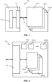
- the memory subsystem 100 includes a system-on-chip (SOC) 110 and one or more memory devices 120 communicating over a link 130.
- the link 130 may comprise a plurality of signal lines including lines to transmit unidirectional signals from the SOC 110 to the memory devices 120 (e.g., clock (CK), chip select (CS), command & address (CA), etc.) and bidirectional directional signals (data (DQ), data strobe (DQS), etc.).
- the SOC 110 includes a memory controller 115 and a PHY block 117.
- the SOC 110 and the memory devices 120 may be in communication with each other over the link 130.
- the memory controller 115 controls the memory devices 120 by exchanging signals to write data to and read data from the memory cells of the memory devices 120.
- Memory device 120 is illustrated in FIG. 2 .
- the memory device 120 may include an input/output (I/O) circuit 210 configured to interface with the memory controller 115.
- the I/O circuit 210 may be an example of means for interfacing.
- the memory controller 115 may be considered to be external to the memory device 120.
- the I/O circuit 210 may also be configured to write data to and read data from a plurality of memory cells.
- the memory cells of the memory device 120 are DRAM cells which store data as charges on capacitors.
- the plurality of memory cells may be partitioned into a plurality of memory banks 220 or simply banks 220. As seen, there may be P banks 220-1 ... 220-P, where P may be any integer greater than zero.
- the memory cells in each bank 220 may be further partitioned into a plurality of blocks or segments. Note that the memory cells within a bank may be segmented in various ways including by row addresses, by column address, or a combination there of.
- the memory device 120 further includes a plurality of mode registers (MR) 230.
- the mode registers 230 define the behavior of the memory device 120. As seen, there may be M mode registers 230-1 ... 230-M, where M may be any integer greater than zero.
- Each mode register 230 is a write type, a read type, or a read/write type.
- the SOC 110 e.g., the memory controller 115
- the memory controller 115 issues also a mode register read (MRR) command to designate a particular read or read/write type mode register, and the I/O circuit 210 reads from the designated mode register and provides the read value to the memory controller 115.
- MRR mode register read
- the memory device 120 may be configured to be in a self-refresh (SR) mode or in an auto-refresh (AR) mode.
- SR self-refresh
- AR auto-refresh
- the memory device 120 enters and exits the SR mode upon respectively receiving the self-refresh-enter (SRE) and the self-refresh-exit (SRX) commands from the memory controller 115.
- SRE self-refresh-enter
- SRX self-refresh-exit
- the memory device 120 when the memory device 120 is in the SR mode, the memory device 120 (e.g., the I/O circuit 210 or some other component) is configured to refresh the memory cells without receiving refresh (REF) commands from the memory controller 115. In this mode, the memory device 120 may generate the necessary refresh pulses through a built-in timer (not shown), and thereby negate the need for the memory controller 115 to issue explicit REF commands.
- the SR mode may be considered as a low power refresh mode since the SOC 110 can be put into an idle state to reduce power consumption.
- the memory controller 115 controls the refresh operation through issuing the REF commands.
- the I/O circuit 210 may be configured to refresh the memory cells upon receiving the REF command from the memory controller 115.
- the auto-refresh current e.g., IDD5
- the memory device 120 includes a partial array refresh enable register and a partial array refresh mask register.
- the bits of the PAR enable register indicate whether one, both, or none of the partial array auto-refresh (PAAR) and the partial array self-refresh (PAAR) are enabled.
- a mask value in the PAR mask register indicates the portions of the memory cells in which the refresh operations are to be skipped as well as portions in which the refresh operations are to be performed.
- the PAR enable register comprises a plurality of enable bits including a PAAR enable bit and a PASR enable bit.
- the PAAR enable bit when set or unset, indicates that the PAAR is enabled or disabled.
- the PASR enable bit when set or unset, indicates that the PASR is enabled or disabled.
- One or more of the mode registers 230 are used to implement the PAR enable register. For each mode register 230 used to implement the PAR enable register, the memory controller 115 issues an MRW command along with a corresponding mode value. The I/O circuit 210 in turn may write the corresponding mode value to that mode register 230. In this way, the PAAR enable bit may be set or unset, and the PASR enable bit may be set or unset.
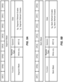
- FIG. 4 illustrates an example of a mode register 230 used to implement the PAR enable register.
- the mode register 230 for the PAR enable register comprises eight operand (OP) bits in which bits OP[1] and OP[0] respectively are the PAAR enable bit and the PASR enable bit.
- the PAAR enable bit when set or unset, indicates that the PAAR is enabled or disabled.
- the PASR enable bit when set or unset, indicates that the PASR is enabled or disabled.
- the value represented by the bits OP[1:0] of the PAR enable register may be referred to as the refresh enable value.
- the PAR mask register may include a plurality of segment mask bits, a plurality of bank mask bits, or both.
- the memory controller 115 may issue an MRW command along with a corresponding mode value.
- the I/O circuit 210 may write the corresponding mode value to that mode register 230. In this way, the mask value may be written to the PAR mask register.
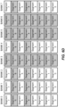
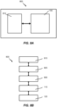
- FIGs. 5A and 5B illustrate examples of the mode registers 230 used to implement the PAR mask register.
- the PAR mask register may include both the segment mask bits and the bank mask bits.
- the eight segment mask bits may be implemented using one of the mode registers 230 as illustrated in FIG. 5A .
- Each OP bit in FIG. 5A may correspond to a segment of a bank, and may indicate whether the refresh is enabled or disabled for the corresponding segment.
- the eight bank mask bits may be implemented using another one of the mode registers 230 as illustrated in FIG. 5B .
- Each OP bit in FIG. 5B may correspond to a bank, and may indicate whether the refresh is enabled or disabled for the corresponding bank.
- the memory device 120 may refresh a subset of the memory cells selected in accordance with the PAR mask register upon receiving the REF command from the memory controller 115.
- the REF command can be a refresh-all-bank (REFab) command or a refresh-per-bank (REFpb) command. Different refresh operations may be carried out depending on the type of the REF command (REFab or REFpb) and on whether the PAR mask includes the segment and/or bank mask bits.
- the memory device 120 may, for each bank, skip the refreshing of each segment whose corresponding segment mask bit indicates that the refreshing is disabled for that segment.
- FIG. 6A An example is illustrated in which the shaded segments represent the segments for which the refresh has been skipped. It is seen that segments 4 and 6 for all for all eight banks are shaded.
- the memory device 120 may, for each bank, skip refreshing that bank when the corresponding bank mask bit indicates that the refreshing is disabled for that bank.
- FIG. 6B An example is illustrated in FIG. 6B in which all segments of banks 3, 5 and 6 are shaded.
- the refresh operation may be skipped for a segment of a bank when both of its corresponding bank and segments mask bits indicate that the refresh is disabled.
- FIG. 6C An example is illustrated in FIG. 6C . Note that if the refresh is skipped for a segment only when both of its bank and segment mask bits indicate that the refresh is disabled, then the first scenario of FIG. 6A may be recreated by enabling all bank mask bits while disabling the segment mask bits of segments 4 and 6, and the second scenario of FIG. 6B may be recreated by enabling all segment mask bits while disabling the bank mask bits of banks 3, 5 and 6.
- the refresh operation may be skipped for a segment of a bank when either of its corresponding bank mask bit or its corresponding segment mask bit indicates that the refresh is disabled.
- FIG. 6D An example is illustrated in FIG. 6D . Note that if the refresh is skipped for a segment of a bank when either of its bank or its segment mask bit indicates that the refresh is disabled, then the first scenario of FIG. 6A may be recreated by disabling all bank mask bits while disabling the segment mask bits of segments 4 and 6, and the second scenario of FIG. 6B may be recreated by disabling all segment mask bits while disabling the bank mask bits of banks 3, 5 and 6.
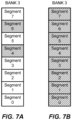
- the memory device 120 is in the AR mode, the PAAR is enabled, and the REF command is the refresh-per-bank REFpb command (as opposed to the REFab command in the scenarios of FIGs. 6A - 6D ).
- the segment masking assume that segment mask bits indicate that the refreshing is disabled for segments 4 and 6.
- the bank masking assume that the bank mask bits indicate that the refreshing is disabled for banks 3, 5 and 6.
- bank 3 is the current bank for which the REFpb command applies.
- the memory device 120 may skip the refreshing of each segment of the current bank - bank 3 - whose corresponding segment mask bit indicates that the refresh is disabled.
- FIG. 7A An example is illustrated in FIG. 7A . As seen, the refresh operations for segments 4 and 6 of bank 3 are skipped. When only the segment masking is applied, then by stepping through eight REFpb commands, results similar to FIG. 6A may be achieved.
- the memory device 120 may skip refreshing of the current bank in its entirety if the corresponding bank mask bit indicates the refresh is disabled.
- FIG. 7B An example is illustrated in FIG. 7B . As seen, the refresh operations are skipped for all segments of bank 3. When only the bank masking is applied, then by stepping through eight REFpb commands, results similar to FIG. 6B may be achieved.
- both the bank and the segments mask bits may be applied for the REFpb command.
- the segment masking may be applied to skip refreshing of selected segments (e.g., segments 4 and 6) if the refresh is disabled for the current bank (e.g., bank 3).
- the refresh is enabled for the current bank, the entirety of the current bank may be refreshed regardless of the segment mask, i.e., no skipping of refresh for any segment of the current bank (not shown). In this instance, by stepping through eight REFpb commands, results similar to FIG. 6C may be achieved.
- the refresh is skipped for a segment of a bank when either of its bank or segment mask bit indicates that the refresh is disabled.
- the segment masking may be applied to skip refreshing of selected segments (e.g., segments 4 and 6) regardless of whether the refresh is enabled or disabled for the current bank (e.g., bank 3).
- the current bank e.g., bank 3
- the same PAR mask register i.e., the same one or more mode registers 230, may be used when the memory device 120 is in the SR mode. While in the SR mode, the memory device 120 may internally refresh the memory cells without the need to receive explicit REF commands from the memory controller 115. If the PASR is enabled (e.g., the PASR enable bit of the PAR enable register is set) while in the SR mode, the memory device 120 may refresh the subset of the memory cells (e.g., selected banks and/or segments) in accordance with the PAR mask register.
- the memory controller 115 may issue the MRW commands for the PAR enable register, and the I/O circuit 210 may write the refresh enable value in the PAR enable register to set the PASR enable bit.
- the memory controller 115 may also issue the MRW commands for the PAR mask register, and the I/O circuit 210 may write the mask value in the PAR mask register.
- the memory controller 115 may issue the MRW command(s) prior to commanding the mobile device 120 to enter the SR mode.
- the memory device 120 may, for each bank, skip the refreshing of each segment whose corresponding segment mask bit indicates that the refreshing is disabled for that segment. This is similar to the first scenario illustrated in FIG. 6A . If the PAR mask register only includes the bank mask bits or the segment masking is turned off, the memory device 120 may, for each bank, skip the refreshing of that bank when the corresponding bank mask bit indicates that the refresh is disabled for that bank. This is similar to the second scenario illustrated in FIG. 6B .
- the memory device 120 may skip the refresh operations for a segment of a bank when both of its corresponding bank and segments mask bits indicate that the refresh is disabled. This is similar to the third scenario illustrated in FIG. 6C .
- the refresh operation may be skipped for a segment of a bank when either of its corresponding bank mask bit or its corresponding segment mask bit indicates that the refresh is disabled. This is similar to the third scenario illustrated in FIG. 6D .
- FIG. 8A illustrates an example block diagram of a computing system 800 which may include a processor 810 and a memory subsystem 100.
- a computing system 800 may include a processor 810 and a memory subsystem 100.
- other components such as input devices (e.g., keyboards, touch pads), output devices (e.g., displays), and non-volatile storage (e.g., flash, disks) are not shown in FIG. 8A .
- the computing system 800 may include one or more processing units (e.g., CPUs), which are collectively represented by the processor 810.
- the memory subsystem 100 has been described in detail above. As seen, the processor 810 and the memory subsystem 100 may communicate with each other.
- FIG. 8A illustrates an example of a hardware makeup of the computing system 800.
- FIG. 8B illustrates an example of a hierarchical arrangement of the same computing system 800.
- the computing system 800 may comprise an application 815, a high level operating system (HLOS) kernel 825, a memory driver 835, the memory controller 115, and the memory device 120, which may be hierarchically arranged in which the application 815 is at the top and the memory device 120 is at the bottom of the hierarchy. Recall that there can be multiple memory devices 120 controlled by the memory controller 115. But for simplicity of description, one memory device 120 is shown.
- HLOS high level operating system
- the memory controller 115 and the memory device 120 may be largely or even exclusively hardware.
- the application 815, the HLOS kernel 825, and the memory driver 835 may be a combination of hardware and software.
- the processor 810 may execute instructions of the application 815, the HLOS kernel 825, and the memory driver 835.
- the memory controller 115 may be in communication with the memory driver 835.
- the higher level components - the application 815, the HLOS kernel and the memory driver 835 - utilize the PAAR feature of the memory devices 120 to save power consumption.
- the memory driver 835 may save attributes of the memory device 120 into a RAM partition table in which the whole of the memory cells of the memory device 120 are divided into regions.
- the RAM partition may be readable.
- the HLOS kernel may generate a memory topology including power attributes, performance attributes, and group physical addresses based on the RAM partition.
- a user interface may be provided to allow a user of the computing system 800 to configure the conditions upon which a power saving mode is triggered.
- the power saving mode can be triggered based on a threshold battery level.
- the power saving mode may be triggered when the computing system has been at low activity for a threshold amount of time. Multiple thresholds can be defined for different levels of active power savings.
- FIG. 9 illustrates an example runtime interaction among the components of the computing system 800.
- an application 815 such as a system event-handler may detect an event and invoke a call-back to the HLOS kernel 825.
- a user may have exited a user application running on the computing system 800, and the user application data may have been saved to a non-volatile storage. In this instance, the user application data need not be maintained in the memory device 120.
- the HLOS kernel 825 may free up a memory region of the user application data and notify the memory driver 835 of the freed memory region.
- the memory driver 835 may translate the freed memory region into a refresh skip region, in which the refresh skip region comprises one or more portions of the memory cells of the memory device 120 that do not require refreshing.
- the memory driver 835 may provide information on the refresh skip region to the memory controller 115.
- the memory controller 115 may respond by issuing the MRW commands to the memory device 120 to set the PAAR enable bit of the PAR enable register, and to write a mask value corresponding to the refresh skip region to the PAR mask register.
- the memory driver 835 may instruct the memory controller 115 to adjust a refresh interval, e.g., tREFI, based on the freed memory region. For example, when refreshing is skipped for a non-zero portion of the memory cells, less power is consumed, and the memory device 120 can run cooler. Therefore, it may be safe to slow the refreshing rate.
- the memory controller 115 may respond by waiting at least the adjusted refresh interval after issuing one REF command and before issuing another REF command to the memory device 120.
- FIG. 10 illustrates various electronic devices that may be integrated with any of the aforementioned memory subsystem 100.
- a mobile phone device 1002, a laptop computer device 1004, a terminal device 1006 as well as wearable devices, portable systems, that require small form factor, extreme low profile may include a device/package 1000 that incorporates the memory subsystem 100 as described herein.
- the device/package 1000 may be, for example, any of the integrated circuits, dies, integrated devices, integrated device packages, integrated circuit devices, device packages, integrated circuit (IC) packages, package-on-package devices, system in package devices described herein.
- the devices 1002, 1004, 1006 illustrated in FIG. 10 are merely exemplary.
- Other electronic devices may also feature the device/package 1000 including, but not limited to, a group of devices (e.g., electronic devices) that includes mobile devices, hand-held personal communication systems (PCS) units, portable data units such as personal digital assistants, global positioning system (GPS) enabled devices, navigation devices, set top boxes, music players, video players, entertainment units, fixed location data units such as meter reading equipment, communications devices, smartphones, tablet computers, computers, wearable devices, servers, routers, electronic devices implemented in automotive vehicles (e.g., autonomous vehicles), or any other device that stores or retrieves data or computer instructions, or any combination thereof.
- a group of devices e.g., electronic devices
- devices that includes mobile devices, hand-held personal communication systems (PCS) units, portable data units such as personal digital assistants, global positioning system (GPS) enabled devices, navigation devices, set top boxes, music players, video players, entertainment units, fixed location data units such as meter reading equipment, communications devices, smartphones, tablet computers, computers, wearable devices, servers, routers, electronic devices implemented
- a software module may reside in RAM memory, flash memory, ROM memory, EPROM memory, EEPROM memory, registers, hard disk, a removable disk, a CD-ROM, or any other form of storage medium known in the art.
- An exemplary storage medium is coupled with the processor such that the processor can read information from, and write information to, the storage medium. In the alternative, the storage medium may be integral to the processor.
- an aspect can include a computer readable media embodying a method of forming a semiconductor device. Accordingly, the scope of the disclosed subject matter is not limited to illustrated examples and any means for performing the functionality described herein are included.
Description
- The field of the disclosed subject matter relates to memory devices. In particular, the field of the disclosed subject matter relates to partial refresh operations in memory devices to save power.
- Memory devices such as dynamic random access memories (DRAM) are widely used in computing devices, including mobile devices, to store data. To maintain data integrity, DRAMS cells are periodically refreshed. As density and speed of the DRAMs increase, the impact of the refresh operations on DRAM's overall performance and power consumption become more and more non-trivial. The refresh operation impact can be particularly significant in mobile devices since power consumption is of greater concern in such devices.
-
US2005/068826 A1 relates to a method of refreshing several memory banks of a memory device that receives command signals from a memory controller. The method includes monitoring command signals received by a memory device and refreshing the several memory banks based on the monitored command signals. So as to avoid unnecessary power consumption for refreshing particular ones of the several memory banks with irrelevant contents. -
US2012/026813 A1 discusses a device which includes a plurality of memory areas each including a plurality of memory cells required to perform refresh of information stored therein by a plurality of sense amplifiers, a first control circuit determining, in connection with one refresh requirement signal at a time, a number of refresh target memory areas to produce a determined number, a second control circuit controlling, in accordance with the one refresh requirement signal at a time, refresh operation with respect to the refresh-target memory areas, and a third control circuit adjusting, in connection with the refresh operation, an active time-out time interval according to the determined number. The active time-out time interval indicates a time interval from a first time instant when the sense amplifiers are activated to a second time instant when word lines related to the refresh-target memory areas are inactivated. -
US2010/182864 A1 discloses that to provide a plurality of memory banks, each of which is divided into a plurality of segments; a bank address register that designates a memory bank that becomes a refresh target; a segment address register that designates a segment that becomes a refresh target; and a refresh control circuit that prohibits a refresh operation of the memory bank or the segment not designated by at least one of the bank address register and the segment address register. This semiconductor device is capable of designating whether to perform a refresh operation not only in a memory bank unit but also in a segment unit within the memory bank, and thus it achieves a further reduction of the power consumption. -
US2008/037344 A1 discloses that each memory block has a plurality of memory cells, and word lines and bit lines connected to the memory cells. Precharge Switches connect the bit lines to a precharge line. A Switch control circuit controls an operation of the pre charge switches and sets a cutoff function that turns off connection switches in a standby period in which no access operation of the memory cells is performed. Since connections of the bit lines and the precharge switch and those of the bit lines and the sense amplifier are cut off in the standby period, if a short circuit failure is present between a word line and a bit line, a leak current can be prevented from flowing from the word line to a precharge voltage line and so on. -
US2002/191467 A1 discloses that data specifying details of refresh to be executed in the self-refresh mode is stored in a register circuit in a mode register. A refresh period and refresh region are determined according to data stored in register circuit and a refresh control circuit generates a control signal and a refresh address that are required for refresh. Stored data can be stably held in the self-refresh mode in which data holding is performed with reduced current consumption. - An apparatus in accordance with
independent claim 1 is disclosed. - A method for reducing power consumption of an apparatus in accordance with
independent claim 10 is further disclosed - A non-transitory computer-readable medium storing instructions to execute the method of
independent claim 10 in accordance withindependent claim 13 is also disclosed. - Additional refinements to both the method and apparatus are incorporated in the dependent claims.
- The accompanying drawings are presented to aid in the description of examples of one or more aspects of the disclosed subject matter and are provided solely for illustration of the examples and not limitation thereof:
-
FIG. 1 illustrates an example of a memory subsystem; -
FIG. 2 illustrates an example of a memory device; -
FIG. 3 illustrates an example partitioning of a plurality of memory cells of a memory device; -
FIG. 4 illustrates an example of a mode register used to implement a partial array refresh enable register; -
FIGs. 5A and 5B illustrate examples of mode registers used to implement a partial array mask; -
FIGs. 6A - 6D illustrate different scenarios in which refresh operations are performed and skipped based on masking when a refresh-all-banks command is issued when partial array auto-refresh is enabled; -
FIGs. 7A and 7B illustrate different scenarios in which refresh operations are performed and skipped based on masking when a refresh-per-bank command is issued when partial array auto-refresh is enabled; -
FIGs. 8A and 8B respectively illustrate hardware and hierarchical arrangement of an example computing system; -
FIG. 9 illustrates an example runtime interaction among components of a computing system; and -
FIG. 10 illustrates examples of devices with a memory subsystem integrated therein. - Aspects of the subject matter are provided in the following description and related drawings directed to specific examples of the disclosed subject matter.
- The word "exemplary" is used herein to mean "serving as an example, instance, or illustration." Any embodiment described herein as "exemplary" is not necessarily to be construed as preferred or advantageous over other embodiments. Likewise, the term "embodiments" does not require that all embodiments of the disclosed subject matter include the discussed feature, advantage or mode of operation.
The terminology used herein is for the purpose of describing particular examples only and is not intended to be limiting. As used herein, the singular forms "a", "an" and "the" are intended to include the plural forms as well, unless the context clearly indicates otherwise. It will be further understood that the terms "comprises", "comprising,", "includes" and/or "including", when used herein, specify the presence of stated features, integers, processes, operations, elements, and/or components, but do not preclude the presence or addition of one or more other features, integers, processes, operations, elements, components, and/or groups thereof. - Further, many examples are described in terms of sequences of actions to be performed by, for example, elements of a computing device. It will be recognized that various actions described herein can be performed by specific circuits (e.g., application specific integrated circuits (ASICs)), by program instructions being executed by one or more processors, or by a combination of both. Additionally, these sequence of actions described herein can be considered to be embodied entirely within any form of computer readable storage medium having stored therein a corresponding set of computer instructions that upon execution would cause an associated processor to perform the functionality described herein. Thus, the various aspects may be embodied in a number of different forms, all of which have been contemplated to be within the scope of the claimed subject matter. In addition, for each of the examples described herein, the corresponding form of any such examples may be described herein as, for example, "logic configured to" perform the described action.
- A cell of a DRAM typically includes an access transistor and a capacitor. Data is stored as an electrically charge in the capacitor. Over time, the charge in the capacitor leaks. To retain the data in the leaky capacitor, periodic refreshes are performed which consume power. In mobile devices, power consumed to perform refreshes can be of a significant concern.
- DRAM devices including mobile DRAM devices usually support two refresh methods - self-refresh (SR) and auto-refresh (AR). SR is used when the DRAM device is in idle or low power state. In the JEDEC (Joint Electron Device Engineering Council) LPDDR4 (Low Power Double Data Rate 4) standard document JESD209-4A, a DRAM device enters and exits the SR mode when it receives self-refresh enter (SRE) and self-refresh exit (SRX) commands from a memory controller. The DRAM device includes a built-in timer which allows it to accommodate the self-refresh operation. When in the SR mode, the SDRAM device can retain data without receiving a refresh command from the memory controller.
- To reduce the self-refresh current ("IDD6" in JEDEC), and hence reduce the self-refresh power consumed, a mobile DRAM device provides a partial array self-refresh (PASR) function which executes a partial array refresh (PAR) during the SR mode. In PASR, the memory controller programs the mobile DRAM device to refresh only a portion of the memory through a PASR mask.
- When the DRAM device is an active state, auto-refresh is used to retain the DRAM cell data. In the AR mode, the memory controller provides an explicit refresh REF command to the mobile DRAM device. To reduce the auto-refresh current ("IDD5" in JEDEC), existing solutions focus on controlling the auto refresh rate tREFI based on temperature. As an illustration, as the device's temperature decreases, the auto refresh rate may also slow down, for example, to half the normal refresh rate or 2 ∗ tREFI. In effect, the overall IDD5 consumption is reduced in conventional solutions by lengthening the time in between the refreshes, e.g., by slowing down the rate of the REF commands being issued.
- However, it is proposed to allow partial array refreshes even when the memory device is in the active state. To state it another way, a partial array auto-refresh (PAAR) can be enabled in which the refresh is skipped for some of the memory cells during the refresh operation. In this way, the auto-refresh current can be reduced.
- A memory subsystem according to the present invention is illustrated in
FIG. 1 . Thememory subsystem 100 includes a system-on-chip (SOC) 110 and one ormore memory devices 120 communicating over alink 130. In reality, thelink 130 may comprise a plurality of signal lines including lines to transmit unidirectional signals from theSOC 110 to the memory devices 120 (e.g., clock (CK), chip select (CS), command & address (CA), etc.) and bidirectional directional signals (data (DQ), data strobe (DQS), etc.). - The
SOC 110 includes amemory controller 115 and aPHY block 117. TheSOC 110 and thememory devices 120 may be in communication with each other over thelink 130. In particular, thememory controller 115 controls thememory devices 120 by exchanging signals to write data to and read data from the memory cells of thememory devices 120. - As seen in the figure, there may be N memory devices 120-1 ... 120-N, where N may be any integer greater than zero.
Memory device 120 is illustrated inFIG. 2 . As seen, thememory device 120 may include an input/output (I/O)circuit 210 configured to interface with thememory controller 115. The I/O circuit 210 may be an example of means for interfacing. Thememory controller 115 may be considered to be external to thememory device 120. The I/O circuit 210 may also be configured to write data to and read data from a plurality of memory cells. The memory cells of thememory device 120 are DRAM cells which store data as charges on capacitors. - In an aspect, the plurality of memory cells may be partitioned into a plurality of
memory banks 220 or simplybanks 220. As seen, there may be P banks 220-1 ... 220-P, where P may be any integer greater than zero. The memory cells in eachbank 220 may be further partitioned into a plurality of blocks or segments. Note that the memory cells within a bank may be segmented in various ways including by row addresses, by column address, or a combination there of.FIG. 3 illustrates an example partitioning of the plurality of memory cells of thememory device 120. In this figure, it is assumed that there are eight banks, i.e, P = 8. Also, within each bank, it is assumed that there are eight segments per bank. Of course, this is merely an example, and is not a limitation. - Referring back to
FIG. 2 , thememory device 120 further includes a plurality of mode registers (MR) 230. The mode registers 230 define the behavior of thememory device 120. As seen, there may be M mode registers 230-1 ... 230-M, where M may be any integer greater than zero. Eachmode register 230 is a write type, a read type, or a read/write type. The SOC 110 (e.g., the memory controller 115) issues a mode register write (MRW) command to designate a particular write or read/write type mode register along with a mode value, and the I/O circuit 210 may write the received mode value to the designated mode register. Thememory controller 115 issues also a mode register read (MRR) command to designate a particular read or read/write type mode register, and the I/O circuit 210 reads from the designated mode register and provides the read value to thememory controller 115. - Because the memory cells of the
memory device 120 are DRAM cells, periodic refreshes are performed to maintain integrity of data stored in the cells. Thememory device 120 may be configured to be in a self-refresh (SR) mode or in an auto-refresh (AR) mode. In an aspect, thememory device 120 enters and exits the SR mode upon respectively receiving the self-refresh-enter (SRE) and the self-refresh-exit (SRX) commands from thememory controller 115. - As indicated, when the
memory device 120 is in the SR mode, the memory device 120 (e.g., the I/O circuit 210 or some other component) is configured to refresh the memory cells without receiving refresh (REF) commands from thememory controller 115. In this mode, thememory device 120 may generate the necessary refresh pulses through a built-in timer (not shown), and thereby negate the need for thememory controller 115 to issue explicit REF commands. The SR mode may be considered as a low power refresh mode since theSOC 110 can be put into an idle state to reduce power consumption. - On the other hand, when the
memory device 120 is in the active state, i.e., when it is in the AR mode, thememory controller 115 controls the refresh operation through issuing the REF commands. The I/O circuit 210 may be configured to refresh the memory cells upon receiving the REF command from thememory controller 115. To reduce the consumption of the auto-refresh current (e.g., IDD5), it is proposed to enable thememory device 120 to refresh a subset - less than all - of the memory cells when thememory controller 115 issues the REF command. That is, it is proposed allow partial array refresh in which the refresh operation is skipped for a non-zero number of the memory cells. - Masking is used to specify the portions of the memory cells for which the refresh operations are to be skipped and other portions for which the refresh operations are to be performed. To enable refresh masking, the
memory device 120 includes a partial array refresh enable register and a partial array refresh mask register. The bits of the PAR enable register indicate whether one, both, or none of the partial array auto-refresh (PAAR) and the partial array self-refresh (PAAR) are enabled. A mask value in the PAR mask register indicates the portions of the memory cells in which the refresh operations are to be skipped as well as portions in which the refresh operations are to be performed. - The PAR enable register comprises a plurality of enable bits including a PAAR enable bit and a PASR enable bit. The PAAR enable bit, when set or unset, indicates that the PAAR is enabled or disabled. Similarly, the PASR enable bit, when set or unset, indicates that the PASR is enabled or disabled. One or more of the mode registers 230 are used to implement the PAR enable register. For each
mode register 230 used to implement the PAR enable register, thememory controller 115 issues an MRW command along with a corresponding mode value. The I/O circuit 210 in turn may write the corresponding mode value to thatmode register 230. In this way, the PAAR enable bit may be set or unset, and the PASR enable bit may be set or unset. -
FIG. 4 illustrates an example of amode register 230 used to implement the PAR enable register. In this example, it is assumed that themode register 230 for the PAR enable register comprises eight operand (OP) bits in which bits OP[1] and OP[0] respectively are the PAAR enable bit and the PASR enable bit. The PAAR enable bit, when set or unset, indicates that the PAAR is enabled or disabled. Similarly, the PASR enable bit, when set or unset, indicates that the PASR is enabled or disabled. The value represented by the bits OP[1:0] of the PAR enable register may be referred to as the refresh enable value. - Different one or more of the mode registers 230 may be used to implement the PAR mask register. The PAR mask register may include a plurality of segment mask bits, a plurality of bank mask bits, or both. For each
mode register 230 used to implement the PAR mask register, thememory controller 115 may issue an MRW command along with a corresponding mode value. In turn, the I/O circuit 210 may write the corresponding mode value to thatmode register 230. In this way, the mask value may be written to the PAR mask register. -
FIGs. 5A and 5B illustrate examples of the mode registers 230 used to implement the PAR mask register. In this example, the assumption is that the memory cells are partitioned into eight banks and eight segments per bank as illustrated inFIG. 3 . Therefore, in this instance, the PAR mask register may include both the segment mask bits and the bank mask bits. The eight segment mask bits may be implemented using one of the mode registers 230 as illustrated inFIG. 5A . Each OP bit inFIG. 5A may correspond to a segment of a bank, and may indicate whether the refresh is enabled or disabled for the corresponding segment. The eight bank mask bits may be implemented using another one of the mode registers 230 as illustrated inFIG. 5B . Each OP bit inFIG. 5B may correspond to a bank, and may indicate whether the refresh is enabled or disabled for the corresponding bank. - Of course, this is merely an example and should not be taken as limiting. If the memory cells are partitioned in segments only or in banks only, then a
single mode register 230 may be sufficient to implement the PAR mask register. If the memory cells are partitioned in further ways, then more mode registers 230 may be necessary for the PAR mask register implementation. - Referring back to
FIGs. 5A and 5B , when thememory device 120 is in the AR mode and the PAAR is enabled (i.e., the PAAR enable bit of the PAR enable register is set) thememory device 120 may refresh a subset of the memory cells selected in accordance with the PAR mask register upon receiving the REF command from thememory controller 115. The REF command can be a refresh-all-bank (REFab) command or a refresh-per-bank (REFpb) command. Different refresh operations may be carried out depending on the type of the REF command (REFab or REFpb) and on whether the PAR mask includes the segment and/or bank mask bits. - In first through fourth scenarios illustrated in
FIGs. 6A - 6D , it may be assumed that thememory device 120 is in the AR mode, the PAAR is enabled, and the REF command is the refresh-all-banks REFab command. Also, if the segment masking is applied, assume that segment mask bits indicate that the refreshing is disabled forsegments banks - In the first scenario, it may be assumed that only the segment masking is applied. This may be because the PAAR mask register only includes the segment mask bits or the bank masking is turned off. In this first scenario, the
memory device 120 may, for each bank, skip the refreshing of each segment whose corresponding segment mask bit indicates that the refreshing is disabled for that segment. An example is illustrated inFIG. 6A in which the shaded segments represent the segments for which the refresh has been skipped. It is seen thatsegments - In the second scenario, it may be assumed that only the bank masking is applied. This may be because the PAAR mask register only includes the banks mask bits or the segment masking is turned off. In the second scenario, the
memory device 120 may, for each bank, skip refreshing that bank when the corresponding bank mask bit indicates that the refreshing is disabled for that bank. An example is illustrated inFIG. 6B in which all segments ofbanks - In the third scenario, it may be assumed that both the bank and segment masking are applied. In the third scenario, the refresh operation may be skipped for a segment of a bank when both of its corresponding bank and segments mask bits indicate that the refresh is disabled. An example is illustrated in
FIG. 6C . Note that if the refresh is skipped for a segment only when both of its bank and segment mask bits indicate that the refresh is disabled, then the first scenario ofFIG. 6A may be recreated by enabling all bank mask bits while disabling the segment mask bits ofsegments FIG. 6B may be recreated by enabling all segment mask bits while disabling the bank mask bits ofbanks - In the fourth scenario, it may also be assumed that both the bank and segment masking are applied. But in the fourth scenario, the refresh operation may be skipped for a segment of a bank when either of its corresponding bank mask bit or its corresponding segment mask bit indicates that the refresh is disabled. An example is illustrated in
FIG. 6D . Note that if the refresh is skipped for a segment of a bank when either of its bank or its segment mask bit indicates that the refresh is disabled, then the first scenario ofFIG. 6A may be recreated by disabling all bank mask bits while disabling the segment mask bits ofsegments FIG. 6B may be recreated by disabling all segment mask bits while disabling the bank mask bits ofbanks - In fifth and sixth scenarios illustrated in
FIGs. 7A - 7B , it may be assumed that thememory device 120 is in the AR mode, the PAAR is enabled, and the REF command is the refresh-per-bank REFpb command (as opposed to the REFab command in the scenarios ofFIGs. 6A - 6D ). If the segment masking is applied, assume that segment mask bits indicate that the refreshing is disabled forsegments banks bank 3 is the current bank for which the REFpb command applies. - In the fifth scenario, like the first scenario, it may be assumed that only the segment masking is applied. In this fifth scenario, the
memory device 120 may skip the refreshing of each segment of the current bank - bank 3 - whose corresponding segment mask bit indicates that the refresh is disabled. An example is illustrated inFIG. 7A . As seen, the refresh operations forsegments bank 3 are skipped. When only the segment masking is applied, then by stepping through eight REFpb commands, results similar toFIG. 6A may be achieved. - In the sixth scenario, like the second scenario, it may be assumed that only the bank masking is applied. In the sixth scenario, the
memory device 120 may skip refreshing of the current bank in its entirety if the corresponding bank mask bit indicates the refresh is disabled. An example is illustrated inFIG. 7B . As seen, the refresh operations are skipped for all segments ofbank 3. When only the bank masking is applied, then by stepping through eight REFpb commands, results similar toFIG. 6B may be achieved. - While not specifically illustrated, both the bank and the segments mask bits may be applied for the REFpb command. In one scenario, assume that the refresh is skipped for a segment of a bank only when both of its bank and segment mask bits indicate that the refresh is disabled. In this scenario, the segment masking may be applied to skip refreshing of selected segments (e.g.,
segments 4 and 6) if the refresh is disabled for the current bank (e.g., bank 3). On the other hand, if the refresh is enabled for the current bank, the entirety of the current bank may be refreshed regardless of the segment mask, i.e., no skipping of refresh for any segment of the current bank (not shown). In this instance, by stepping through eight REFpb commands, results similar toFIG. 6C may be achieved. - In another scenario, assume that the refresh is skipped for a segment of a bank when either of its bank or segment mask bit indicates that the refresh is disabled. In this scenario, the segment masking may be applied to skip refreshing of selected segments (e.g.,
segments 4 and 6) regardless of whether the refresh is enabled or disabled for the current bank (e.g., bank 3). In this instance, by stepping through eight REFpb commands, results similar toFIG. 6D may be achieved. - In an aspect, the same PAR mask register, i.e., the same one or more mode registers 230, may be used when the
memory device 120 is in the SR mode. While in the SR mode, thememory device 120 may internally refresh the memory cells without the need to receive explicit REF commands from thememory controller 115. If the PASR is enabled (e.g., the PASR enable bit of the PAR enable register is set) while in the SR mode, thememory device 120 may refresh the subset of the memory cells (e.g., selected banks and/or segments) in accordance with the PAR mask register. - The
memory controller 115 may issue the MRW commands for the PAR enable register, and the I/O circuit 210 may write the refresh enable value in the PAR enable register to set the PASR enable bit. Thememory controller 115 may also issue the MRW commands for the PAR mask register, and the I/O circuit 210 may write the mask value in the PAR mask register. Thememory controller 115 may issue the MRW command(s) prior to commanding themobile device 120 to enter the SR mode. - While in the SR mode, if the PAR mask register only includes the segment mask bits or the bank masking is turned off, the
memory device 120 may, for each bank, skip the refreshing of each segment whose corresponding segment mask bit indicates that the refreshing is disabled for that segment. This is similar to the first scenario illustrated inFIG. 6A . If the PAR mask register only includes the bank mask bits or the segment masking is turned off, thememory device 120 may, for each bank, skip the refreshing of that bank when the corresponding bank mask bit indicates that the refresh is disabled for that bank. This is similar to the second scenario illustrated inFIG. 6B . - If the PAR mask register includes both the bank and mask bits, the
memory device 120 may skip the refresh operations for a segment of a bank when both of its corresponding bank and segments mask bits indicate that the refresh is disabled. This is similar to the third scenario illustrated inFIG. 6C . Alternatively, the refresh operation may be skipped for a segment of a bank when either of its corresponding bank mask bit or its corresponding segment mask bit indicates that the refresh is disabled. This is similar to the third scenario illustrated inFIG. 6D . -
FIG. 8A illustrates an example block diagram of acomputing system 800 which may include aprocessor 810 and amemory subsystem 100. For simplicity, other components such as input devices (e.g., keyboards, touch pads), output devices (e.g., displays), and non-volatile storage (e.g., flash, disks) are not shown inFIG. 8A . Also, thecomputing system 800 may include one or more processing units (e.g., CPUs), which are collectively represented by theprocessor 810. Thememory subsystem 100 has been described in detail above. As seen, theprocessor 810 and thememory subsystem 100 may communicate with each other. -
FIG. 8A illustrates an example of a hardware makeup of thecomputing system 800.FIG. 8B illustrates an example of a hierarchical arrangement of thesame computing system 800. Thecomputing system 800 may comprise anapplication 815, a high level operating system (HLOS)kernel 825, amemory driver 835, thememory controller 115, and thememory device 120, which may be hierarchically arranged in which theapplication 815 is at the top and thememory device 120 is at the bottom of the hierarchy. Recall that there can bemultiple memory devices 120 controlled by thememory controller 115. But for simplicity of description, onememory device 120 is shown. - The
memory controller 115 and thememory device 120 may be largely or even exclusively hardware. Theapplication 815, theHLOS kernel 825, and thememory driver 835 may be a combination of hardware and software. For example, theprocessor 810 may execute instructions of theapplication 815, theHLOS kernel 825, and thememory driver 835. As seen inFIG. 8 , thememory controller 115 may be in communication with thememory driver 835. - In an aspect, it is proposed that the higher level components - the
application 815, the HLOS kernel and the memory driver 835 - utilize the PAAR feature of thememory devices 120 to save power consumption. At boot up, thememory driver 835 may save attributes of thememory device 120 into a RAM partition table in which the whole of the memory cells of thememory device 120 are divided into regions. The RAM partition may be readable. The HLOS kernel may generate a memory topology including power attributes, performance attributes, and group physical addresses based on the RAM partition. - A user interface may be provided to allow a user of the
computing system 800 to configure the conditions upon which a power saving mode is triggered. For example, the power saving mode can be triggered based on a threshold battery level. Alternatively or in addition thereto, the power saving mode may be triggered when the computing system has been at low activity for a threshold amount of time. Multiple thresholds can be defined for different levels of active power savings. -
FIG. 9 illustrates an example runtime interaction among the components of thecomputing system 800. Inblock 910, anapplication 815 such as a system event-handler may detect an event and invoke a call-back to theHLOS kernel 825. For example, a user may have exited a user application running on thecomputing system 800, and the user application data may have been saved to a non-volatile storage. In this instance, the user application data need not be maintained in thememory device 120. Inblock 920, theHLOS kernel 825 may free up a memory region of the user application data and notify thememory driver 835 of the freed memory region. - In
block 930, thememory driver 835 may translate the freed memory region into a refresh skip region, in which the refresh skip region comprises one or more portions of the memory cells of thememory device 120 that do not require refreshing. Inblock 940, thememory driver 835 may provide information on the refresh skip region to thememory controller 115. Inblock 945, thememory controller 115 may respond by issuing the MRW commands to thememory device 120 to set the PAAR enable bit of the PAR enable register, and to write a mask value corresponding to the refresh skip region to the PAR mask register. - In
block 950, thememory driver 835 may instruct thememory controller 115 to adjust a refresh interval, e.g., tREFI, based on the freed memory region. For example, when refreshing is skipped for a non-zero portion of the memory cells, less power is consumed, and thememory device 120 can run cooler. Therefore, it may be safe to slow the refreshing rate. Inblock 955, thememory controller 115 may respond by waiting at least the adjusted refresh interval after issuing one REF command and before issuing another REF command to thememory device 120. -
FIG. 10 illustrates various electronic devices that may be integrated with any of theaforementioned memory subsystem 100. For example, amobile phone device 1002, alaptop computer device 1004, aterminal device 1006 as well as wearable devices, portable systems, that require small form factor, extreme low profile, may include a device/package 1000 that incorporates thememory subsystem 100 as described herein. The device/package 1000 may be, for example, any of the integrated circuits, dies, integrated devices, integrated device packages, integrated circuit devices, device packages, integrated circuit (IC) packages, package-on-package devices, system in package devices described herein. Thedevices FIG. 10 are merely exemplary. Other electronic devices may also feature the device/package 1000 including, but not limited to, a group of devices (e.g., electronic devices) that includes mobile devices, hand-held personal communication systems (PCS) units, portable data units such as personal digital assistants, global positioning system (GPS) enabled devices, navigation devices, set top boxes, music players, video players, entertainment units, fixed location data units such as meter reading equipment, communications devices, smartphones, tablet computers, computers, wearable devices, servers, routers, electronic devices implemented in automotive vehicles (e.g., autonomous vehicles), or any other device that stores or retrieves data or computer instructions, or any combination thereof. - Those of skill in the art will appreciate that information and signals may be represented using any of a variety of different technologies and techniques. For example, data, instructions, commands, information, signals, bits, symbols, and chips that may be referenced throughout the above description may be represented by voltages, currents, electromagnetic waves, magnetic fields or particles, optical fields or particles, or any combination thereof.
- Further, those of skill in the art will appreciate that the various illustrative logical blocks, modules, circuits, and algorithms described in connection with the examples disclosed herein may be implemented as electronic hardware, computer software, or combinations of both. To clearly illustrate this interchangeability of hardware and software, various illustrative components, blocks, modules, circuits, and methods have been described above generally in terms of their functionality. Whether such functionality is implemented as hardware or software depends upon the particular application and design constraints imposed on the overall system. Skilled artisans may implement the described functionality in varying ways for each particular application, but such implementation decisions should not be interpreted as causing a departure from the scope of the present disclosure.
- The methods, sequences and/or algorithms described in connection with the examples disclosed herein may be embodied directly in hardware, in a software module executed by a processor, or in a combination of the two. A software module may reside in RAM memory, flash memory, ROM memory, EPROM memory, EEPROM memory, registers, hard disk, a removable disk, a CD-ROM, or any other form of storage medium known in the art. An exemplary storage medium is coupled with the processor such that the processor can read information from, and write information to, the storage medium. In the alternative, the storage medium may be integral to the processor.
- Accordingly, an aspect can include a computer readable media embodying a method of forming a semiconductor device. Accordingly, the scope of the disclosed subject matter is not limited to illustrated examples and any means for performing the functionality described herein are included.
- While the foregoing disclosure shows illustrative examples, it should be noted that various changes and modifications could be made herein without departing from the scope of the disclosed subject matter as defined by the appended claims. The functions, processes and/or actions of the method claims in accordance with the examples described herein need not be performed in any particular order. Furthermore, although elements of the disclosed subject matter may be described or claimed in the singular, the plural is contemplated unless limitation to the singular is explicitly stated.
Claims (13)
- An apparatus, comprising a system-on-chip, SOC, (110) and a memory device (120) configured to communicate with each other over a link (130) wherein the SOC is configured to provide commands to the memory device over the link (130), wherein
the memory device (120), comprises:a plurality of DRAM memory cells; and a plurality of mode registers, MR, configured to implement a partial array refresh, PAR, enable register and a PAR mask register, the PAR enable register comprising a plurality of enable bits including a partial array self-refresh, PASR, enable bit and a partial array auto-refresh, PAAR, enable bit, the PASR enable bit when set indicating that PASR is enabled, and the PAAR enable bit when set indicating that PAAR is enabled; andwherein the SOC is configured toissue a mode register write, MRW, command with a corresponding mode value to the memory device so as to set the PAAR enable bit of the PAR enable register;
issue a mode register write, MRW, command with a corresponding mode value to the memory device so as to cause a mask value to be written to the PAR mask register, the mask value corresponding to a refresh skip region; and
issue a REF command to the memory device; andwherein the memory device is configured to skip refreshing of the refresh skip region based on the PAR mask register when the REF command is issued by the SOC and the PAAR enable bit is set. - The apparatus of claim 1,wherein the plurality of DRAM memory cells is partitioned into a plurality of banks, each bank comprising a plurality of segments,wherein the PAR mask register comprises a plurality of segment mask bits, each segment mask bit corresponding to a segment of a bank and indicating whether a refresh is enabled or disabled for the corresponding segment, andwherein the memory device is configured to skip refreshing of each segment of a current bank whose corresponding segment mask bit indicates that the refresh is disabled when the REF command is a refresh-per-bank command and the PAAR enable bit is set.
- The apparatus of claim 2,wherein the plurality of DRAM memory cells is partitioned into a plurality of banks,wherein the PAR mask register comprises a plurality of bank mask bits, each bank mask bit corresponding to a bank and indicating whether a refresh is enabled or disabled for the corresponding bank, andwherein the memory device is configured to skip the refreshing of a current bank when the corresponding bank mask bit indicates that the refresh is disabled when the PAAR is enabled, and the REF command is a refresh-per-bank command.
- The apparatus of claim 2,wherein the plurality of DRAM memory cells is partitioned into a plurality of banks, each bank comprising a plurality of segments,wherein the PAR mask register comprises a plurality of segment mask bits, each segment mask bit corresponding to a segment of a bank and indicating whether a refresh is enabled or disabled for the corresponding segment, andwherein the memory device is configured to, for each bank, skip refreshing of each segment of that bank whose corresponding segment mask bit indicates that the refresh is disabled when the PAAR is enabled, and the REF command is a refresh-all-banks command.
- The apparatus of claim 2,wherein the plurality of DRAM memory cells is partitioned into a plurality of banks,wherein the PAR mask register comprises a plurality of bank mask bits, each bank mask bit corresponding to a bank and indicating whether a refresh is enabled or disabled for the corresponding bank, andwherein the memory device is configured to skip the refreshing of each bank whose corresponding bank mask bit indicates that the refresh is disabled the PAAR is enabled, and the REF command is a refresh-all-banks command,.
- The apparatus of claim 2,wherein the plurality of DRAM memory cells is partitioned into a plurality of banks, each bank comprising a plurality of segments,wherein the PAR mask register includes a plurality of bank mask bits and a plurality of segment mask bits, each bank mask bit corresponding to a bank and indicating whether a refresh is enabled or disabled for the corresponding bank, and each segment mask bit corresponding to a segment and indicating whether a refresh is enabled or disabled for the corresponding segment, andwherein the memory device is configured toskip refreshing of each bank whose corresponding bank mask bit indicates that the refresh is disabled for that bank, andfor each bank whose corresponding bank mask bit indicates that the refresh is enabled for that bank, skip refreshing each segment of that bank whose corresponding segment mask bit indicates that the refresh is disabled when the PASR is enabled.
- The apparatus of any previous claim, wherein the SOC is configured to receive the refresh skip region from a memory driver of a computing system, and
issue the MRW commands to set the PAAR enable bit of the PAR enable register and to set the mask value indicating the refresh skip region subsequent to receiving the refresh skip region from the memory driver. - The apparatus of claim 1, wherein the SOC is configured to adjust a duration in between issuing the REF commands to the memory device based on the refresh skip region.
- The apparatus of any previous claim wherein the apparatus is incorporated into a device selected from a group consisting of a music player, a video player, an entertainment unit, a navigation device, a communications device, a mobile device, a mobile phone, a smart phone a personal digital assistant, a fixed location terminal, a tablet computer, a computer, a wearable device, a laptop computer, a server, and a device in an automotive vehicle.
- A method for reducing memory power consumption of an apparatus,wherein the apparatus comprises a system-on-chip, SOC, (110) and a memory device (120) configured to communicate with each other over a link (130),wherein the SOC is configured to provide commands to the memory device over the link,wherein the memory device comprises:a plurality of DRAM memory cells; anda plurality of mode registers, MR, configured to implement a partial array refresh, PAR, enable register and a PAR mask register, the PAR enable register comprising a plurality of enable bits including a partial array self-refresh, PASR, enable bit and a partial array auto-refresh, PAAR, enable bit, the PASR enable bit when set indicating that PASR is enabled, and the PAAR enable bit when set indicating that PAAR is enabled, andwherein the method comprises:issuing, by the SOC, for each mode register used to implement the PAR enable register, a mode register write, MRW, command with a corresponding mode value to the memory device so as to set the PAAR enable bit of the PAR enable register;issuing, by the SOC, for each mode register used to implement the PAR mask register, a mode register write, MRW, command with a corresponding mode value to the memory device so as to cause a mask value to be written to the PAR mask register, the mask value corresponding to a refresh skip region;issuing, by the SOC, a REF command to the memory device; andskipping, by the memory device, refreshing of the refresh skip region based on the PAR mask register when the REF command is issued by the SOC and the PAAR enable bit is set.
- The method of claim 10,wherein the plurality of memory cells is partitioned into a plurality of banks, each bank comprising a plurality of segments, wherein the PAR mask register comprises a plurality of segment mask bits, each segment mask bit corresponding to a segment of a bank and indicating whether a refresh is enabled or disabled for the corresponding segment, andwherein the skipping the refreshing comprises skipping the refreshing of each segment of a current bank whose corresponding segment mask bit indicates that the refresh is disabled when the REF command is a refresh-per-bank command and the PAAR enable bit is set.
- The method of claim 10,wherein the plurality of memory cells is partitioned into a plurality of banks, each bank comprising a plurality of segments,wherein the PAR mask register comprises a plurality of segment mask bits, each segment mask bit corresponding to a segment of a bank and indicating whether a refresh is enabled or disabled for the corresponding segment, andwherein the skipping the refreshing comprises, for each bank, skipping the refreshing of each segment of that bank whose corresponding segment mask bit indicates that the refresh is disabled when the REF command is a refresh-all-banks command and the PAAR enable bit is set.
- A non-transitory computer-readable medium having stored thereon computer executable instructions which, when executed by a processor, cause the processor to:
implement the method according to any of claims 10 to 12.
Priority Applications (1)
| Application Number | Priority Date | Filing Date | Title |
|---|---|---|---|
| EP23164065.7A EP4220643A1 (en) | 2017-08-02 | 2018-05-25 | Partial refresh technique to save memory refresh power |
Applications Claiming Priority (2)
| Application Number | Priority Date | Filing Date | Title |
|---|---|---|---|
| US15/667,618 US10332582B2 (en) | 2017-08-02 | 2017-08-02 | Partial refresh technique to save memory refresh power |
| PCT/US2018/034659 WO2019027544A1 (en) | 2017-08-02 | 2018-05-25 | Partial refresh technique to save memory refresh power |
Related Child Applications (2)
| Application Number | Title | Priority Date | Filing Date |
|---|---|---|---|
| EP23164065.7A Division EP4220643A1 (en) | 2017-08-02 | 2018-05-25 | Partial refresh technique to save memory refresh power |
| EP23164065.7A Division-Into EP4220643A1 (en) | 2017-08-02 | 2018-05-25 | Partial refresh technique to save memory refresh power |
Publications (2)
| Publication Number | Publication Date |
|---|---|
| EP3662475A1 EP3662475A1 (en) | 2020-06-10 |
| EP3662475B1 true EP3662475B1 (en) | 2023-06-07 |
Family
ID=62631171
Family Applications (2)
| Application Number | Title | Priority Date | Filing Date |
|---|---|---|---|
| EP23164065.7A Pending EP4220643A1 (en) | 2017-08-02 | 2018-05-25 | Partial refresh technique to save memory refresh power |
| EP18731945.4A Active EP3662475B1 (en) | 2017-08-02 | 2018-05-25 | Partial refresh technique to save memory refresh power |
Family Applications Before (1)
| Application Number | Title | Priority Date | Filing Date |
|---|---|---|---|
| EP23164065.7A Pending EP4220643A1 (en) | 2017-08-02 | 2018-05-25 | Partial refresh technique to save memory refresh power |
Country Status (7)
| Country | Link |
|---|---|
| US (4) | US10332582B2 (en) |
| EP (2) | EP4220643A1 (en) |
| CN (2) | CN117524276A (en) |
| BR (1) | BR112020001854A2 (en) |
| SG (1) | SG11201912352RA (en) |
| TW (1) | TWI691958B (en) |
| WO (1) | WO2019027544A1 (en) |
Families Citing this family (50)
| Publication number | Priority date | Publication date | Assignee | Title |
|---|---|---|---|---|
| US10490251B2 (en) | 2017-01-30 | 2019-11-26 | Micron Technology, Inc. | Apparatuses and methods for distributing row hammer refresh events across a memory device |
| US10332582B2 (en) | 2017-08-02 | 2019-06-25 | Qualcomm Incorporated | Partial refresh technique to save memory refresh power |
| CN112106138B (en) | 2018-05-24 | 2024-02-27 | 美光科技公司 | Apparatus and method for pure time adaptive sampling for row hammer refresh sampling |
| US20190378564A1 (en) * | 2018-06-11 | 2019-12-12 | Nanya Technology Corporation | Memory device and operating method thereof |
| US11152050B2 (en) | 2018-06-19 | 2021-10-19 | Micron Technology, Inc. | Apparatuses and methods for multiple row hammer refresh address sequences |
| US10573370B2 (en) | 2018-07-02 | 2020-02-25 | Micron Technology, Inc. | Apparatus and methods for triggering row hammer address sampling |
| US10685696B2 (en) | 2018-10-31 | 2020-06-16 | Micron Technology, Inc. | Apparatuses and methods for access based refresh timing |
| CN113168861A (en) | 2018-12-03 | 2021-07-23 | 美光科技公司 | Semiconductor device for performing row hammer refresh operation |
| CN117198356A (en) * | 2018-12-21 | 2023-12-08 | 美光科技公司 | Apparatus and method for timing interleaving for targeted refresh operations |
| US10957377B2 (en) | 2018-12-26 | 2021-03-23 | Micron Technology, Inc. | Apparatuses and methods for distributed targeted refresh operations |
| US10770127B2 (en) | 2019-02-06 | 2020-09-08 | Micron Technology, Inc. | Apparatuses and methods for managing row access counts |
| GB2578932B (en) * | 2019-02-14 | 2021-02-24 | Imagination Tech Ltd | Allocation of memory |
| US11615831B2 (en) * | 2019-02-26 | 2023-03-28 | Micron Technology, Inc. | Apparatuses and methods for memory mat refresh sequencing |
| US11043254B2 (en) | 2019-03-19 | 2021-06-22 | Micron Technology, Inc. | Semiconductor device having cam that stores address signals |
| US11227649B2 (en) | 2019-04-04 | 2022-01-18 | Micron Technology, Inc. | Apparatuses and methods for staggered timing of targeted refresh operations |
| US11264096B2 (en) | 2019-05-14 | 2022-03-01 | Micron Technology, Inc. | Apparatuses, systems, and methods for a content addressable memory cell with latch and comparator circuits |
| US11158364B2 (en) | 2019-05-31 | 2021-10-26 | Micron Technology, Inc. | Apparatuses and methods for tracking victim rows |
| US11069393B2 (en) | 2019-06-04 | 2021-07-20 | Micron Technology, Inc. | Apparatuses and methods for controlling steal rates |
| US10978132B2 (en) | 2019-06-05 | 2021-04-13 | Micron Technology, Inc. | Apparatuses and methods for staggered timing of skipped refresh operations |
| US11158373B2 (en) | 2019-06-11 | 2021-10-26 | Micron Technology, Inc. | Apparatuses, systems, and methods for determining extremum numerical values |
| US10832792B1 (en) | 2019-07-01 | 2020-11-10 | Micron Technology, Inc. | Apparatuses and methods for adjusting victim data |
| US11139015B2 (en) | 2019-07-01 | 2021-10-05 | Micron Technology, Inc. | Apparatuses and methods for monitoring word line accesses |
| US11386946B2 (en) | 2019-07-16 | 2022-07-12 | Micron Technology, Inc. | Apparatuses and methods for tracking row accesses |
| US10943636B1 (en) | 2019-08-20 | 2021-03-09 | Micron Technology, Inc. | Apparatuses and methods for analog row access tracking |
| US10964378B2 (en) | 2019-08-22 | 2021-03-30 | Micron Technology, Inc. | Apparatus and method including analog accumulator for determining row access rate and target row address used for refresh operation |
| US11200942B2 (en) | 2019-08-23 | 2021-12-14 | Micron Technology, Inc. | Apparatuses and methods for lossy row access counting |
| US11302374B2 (en) | 2019-08-23 | 2022-04-12 | Micron Technology, Inc. | Apparatuses and methods for dynamic refresh allocation |
| US20210064119A1 (en) * | 2019-08-26 | 2021-03-04 | Micron Technology, Inc. | Bank configurable power modes |
| US11302377B2 (en) | 2019-10-16 | 2022-04-12 | Micron Technology, Inc. | Apparatuses and methods for dynamic targeted refresh steals |
| US11868619B2 (en) | 2019-12-20 | 2024-01-09 | Rambus Inc. | Partial array refresh timing |
| US11309010B2 (en) | 2020-08-14 | 2022-04-19 | Micron Technology, Inc. | Apparatuses, systems, and methods for memory directed access pause |
| US11348631B2 (en) | 2020-08-19 | 2022-05-31 | Micron Technology, Inc. | Apparatuses, systems, and methods for identifying victim rows in a memory device which cannot be simultaneously refreshed |
| US11380382B2 (en) | 2020-08-19 | 2022-07-05 | Micron Technology, Inc. | Refresh logic circuit layout having aggressor detector circuit sampling circuit and row hammer refresh control circuit |
| US11222682B1 (en) | 2020-08-31 | 2022-01-11 | Micron Technology, Inc. | Apparatuses and methods for providing refresh addresses |
| EP4002368A4 (en) | 2020-09-22 | 2022-05-25 | Changxin Memory Technologies, Inc. | Memory data refresh method and controller therefor, and memory |
| CN114255799B (en) * | 2020-09-22 | 2023-10-17 | 长鑫存储技术有限公司 | Memory data refreshing method, controller thereof and memory |
| US11557331B2 (en) | 2020-09-23 | 2023-01-17 | Micron Technology, Inc. | Apparatuses and methods for controlling refresh operations |
| US11222686B1 (en) | 2020-11-12 | 2022-01-11 | Micron Technology, Inc. | Apparatuses and methods for controlling refresh timing |
| US11462291B2 (en) | 2020-11-23 | 2022-10-04 | Micron Technology, Inc. | Apparatuses and methods for tracking word line accesses |
| US11264079B1 (en) | 2020-12-18 | 2022-03-01 | Micron Technology, Inc. | Apparatuses and methods for row hammer based cache lockdown |
| US11482275B2 (en) | 2021-01-20 | 2022-10-25 | Micron Technology, Inc. | Apparatuses and methods for dynamically allocated aggressor detection |
| WO2022178772A1 (en) * | 2021-02-25 | 2022-09-01 | 华为技术有限公司 | Memory refresh method, memory, controller, and storage system |
| US11600314B2 (en) | 2021-03-15 | 2023-03-07 | Micron Technology, Inc. | Apparatuses and methods for sketch circuits for refresh binning |
| KR20230025554A (en) | 2021-08-12 | 2023-02-22 | 삼성전자주식회사 | Operating method of host device and storage device and storage device |
| US11664063B2 (en) | 2021-08-12 | 2023-05-30 | Micron Technology, Inc. | Apparatuses and methods for countering memory attacks |
| US11688451B2 (en) | 2021-11-29 | 2023-06-27 | Micron Technology, Inc. | Apparatuses, systems, and methods for main sketch and slim sketch circuit for row address tracking |
| CN114384996B (en) * | 2022-01-14 | 2023-10-24 | 长鑫存储技术有限公司 | Power supply control circuit and control method |
| US20230359373A1 (en) * | 2022-05-03 | 2023-11-09 | Qualcomm Incorporated | Selective refresh for memory devices |
| CN117174131A (en) * | 2022-05-25 | 2023-12-05 | 长鑫存储技术有限公司 | Refresh control circuit, memory and refresh control method |
| CN116543806B (en) * | 2023-06-13 | 2023-11-21 | 长鑫存储技术有限公司 | Refresh masking signal generating circuit, semiconductor memory device, and refresh method thereof |
Family Cites Families (63)
| Publication number | Priority date | Publication date | Assignee | Title |
|---|---|---|---|---|
| JP3400824B2 (en) | 1992-11-06 | 2003-04-28 | 三菱電機株式会社 | Semiconductor storage device |
| JP2001338489A (en) | 2000-05-24 | 2001-12-07 | Mitsubishi Electric Corp | Semiconductor device |
| JP2002064150A (en) * | 2000-06-05 | 2002-02-28 | Mitsubishi Electric Corp | Semiconductor device |
| JP5034149B2 (en) | 2000-10-05 | 2012-09-26 | 富士通セミコンダクター株式会社 | Semiconductor memory and control method thereof |
| US6590822B2 (en) | 2001-05-07 | 2003-07-08 | Samsung Electronics Co., Ltd. | System and method for performing partial array self-refresh operation in a semiconductor memory device |
| JP2002373489A (en) | 2001-06-15 | 2002-12-26 | Mitsubishi Electric Corp | Semiconductor memory |
| US6549479B2 (en) | 2001-06-29 | 2003-04-15 | Micron Technology, Inc. | Memory device and method having reduced-power self-refresh mode |
| KR100437610B1 (en) | 2001-09-20 | 2004-06-30 | 주식회사 하이닉스반도체 | A low power semiconductor memory device with normal mode and partial array self refresh mode |
| US6738861B2 (en) | 2001-09-20 | 2004-05-18 | Intel Corporation | System and method for managing data in memory for reducing power consumption |
| DE10154770B4 (en) | 2001-11-08 | 2004-11-18 | Infineon Technologies Ag | Dynamic memory device with a selection device for the selective fading out of unused memory cells during the refresh |
| US6650587B2 (en) | 2001-11-19 | 2003-11-18 | Micron Technology, Inc. | Partial array self-refresh |
| US6618314B1 (en) * | 2002-03-04 | 2003-09-09 | Cypress Semiconductor Corp. | Method and architecture for reducing the power consumption for memory devices in refresh operations |
| US7043599B1 (en) | 2002-06-20 | 2006-05-09 | Rambus Inc. | Dynamic memory supporting simultaneous refresh and data-access transactions |
| US6920523B2 (en) | 2002-10-07 | 2005-07-19 | Infineon Technologies Ag | Bank address mapping according to bank retention time in dynamic random access memories |
| JP4205396B2 (en) | 2002-10-30 | 2009-01-07 | エルピーダメモリ株式会社 | Semiconductor integrated circuit device |
| JP2004273029A (en) | 2003-03-10 | 2004-09-30 | Sony Corp | Storage device, and refreshing control circuit and refreshing method used for same |
| US6912168B2 (en) | 2003-03-18 | 2005-06-28 | United Memories, Inc. | Non-contiguous masked refresh for an integrated circuit memory |
| US6853591B2 (en) | 2003-03-31 | 2005-02-08 | Micron Technology, Inc. | Circuit and method for decreasing the required refresh rate of DRAM devices |
| KR100605606B1 (en) | 2003-05-29 | 2006-07-28 | 주식회사 하이닉스반도체 | Synchronous self refresh exit control method and circuit in memory device |
| US6956782B2 (en) * | 2003-09-30 | 2005-10-18 | Infineon Technologies Ag | Selective bank refresh |
| KR100621619B1 (en) | 2003-11-14 | 2006-09-13 | 삼성전자주식회사 | Semiconductor memory device for performing refresh operation |
| US7345940B2 (en) * | 2003-11-18 | 2008-03-18 | Infineon Technologies Ag | Method and circuit configuration for refreshing data in a semiconductor memory |
| KR100653688B1 (en) | 2004-04-29 | 2006-12-04 | 삼성전자주식회사 | Semiconductor memory device and refresh method of the same, and memory system for the same |
| KR100611774B1 (en) | 2004-06-03 | 2006-08-10 | 주식회사 하이닉스반도체 | Bank based partial array self refresh apparatus in semiconductor memory device and its method |
| KR20060084071A (en) | 2005-01-17 | 2006-07-24 | 삼성전자주식회사 | Refresh control circuits for use in semiconductor memory and method for control therefore |
| US7702839B2 (en) * | 2005-04-12 | 2010-04-20 | Nokia Corporation | Memory interface for volatile and non-volatile memory devices |
| US7492656B2 (en) * | 2006-04-28 | 2009-02-17 | Mosaid Technologies Incorporated | Dynamic random access memory with fully independent partial array refresh function |
| JP2008065971A (en) | 2006-08-10 | 2008-03-21 | Fujitsu Ltd | Semiconductor memory and memory system |
| JP4299849B2 (en) | 2006-08-22 | 2009-07-22 | エルピーダメモリ株式会社 | Semiconductor memory device and refresh control method thereof |
| JP2008084426A (en) | 2006-09-27 | 2008-04-10 | Fujitsu Ltd | Semiconductor memory and system |
| JP4869011B2 (en) | 2006-09-29 | 2012-02-01 | 富士通セミコンダクター株式会社 | Memory system |
| DE602007009728D1 (en) | 2006-12-22 | 2010-11-18 | Sidense Corp | MASK PROGRAMMABLE ANTI-MIX CONNECTION ARCHITECTURE |
| JP5098391B2 (en) | 2007-03-28 | 2012-12-12 | 富士通セミコンダクター株式会社 | Semiconductor memory, system, and operation method of semiconductor memory |
| US9071246B2 (en) * | 2007-09-14 | 2015-06-30 | Agate Logic, Inc. | Memory controller for heterogeneous configurable integrated circuits |
| KR100899394B1 (en) * | 2007-10-31 | 2009-05-27 | 주식회사 하이닉스반도체 | Refresh controlling circuit |
| US8161356B2 (en) | 2008-03-28 | 2012-04-17 | Intel Corporation | Systems, methods, and apparatuses to save memory self-refresh power |
| US7983108B2 (en) | 2008-08-04 | 2011-07-19 | Micron Technology, Inc. | Row mask addressing |
| CN102369579B (en) | 2008-12-30 | 2015-01-14 | 美光科技公司 | Temperature alert and low rate refresh for a non-volatile memory |
| JP5599977B2 (en) | 2009-01-22 | 2014-10-01 | ピーエスフォー ルクスコ エスエイアールエル | Semiconductor memory device |
| JP2011034632A (en) | 2009-07-31 | 2011-02-17 | Elpida Memory Inc | Semiconductor memory device and method of testing the same |
| US8307270B2 (en) | 2009-09-03 | 2012-11-06 | International Business Machines Corporation | Advanced memory device having improved performance, reduced power and increased reliability |
| US20110296098A1 (en) | 2010-06-01 | 2011-12-01 | Dell Products L.P. | System and Method for Reducing Power Consumption of Memory |
| JP2012033228A (en) | 2010-07-30 | 2012-02-16 | Elpida Memory Inc | Semiconductor device and method for controlling the same |
| US9292426B2 (en) | 2010-09-24 | 2016-03-22 | Intel Corporation | Fast exit from DRAM self-refresh |
| US8705302B2 (en) | 2010-09-24 | 2014-04-22 | Samsung Electronics Co., Ltd. | Semiconductor memory devices having self-refresh capability |
| US20130100755A1 (en) * | 2011-10-21 | 2013-04-25 | Samsung Electronics Co., Ltd. | Semiconductor memory device implementing comprehensive partial array self refresh scheme |
| EP2620838B1 (en) | 2012-01-26 | 2015-04-22 | ST-Ericsson SA | Automatic partial array self-refresh |
| JP2013196740A (en) | 2012-03-22 | 2013-09-30 | Toshiba Corp | Semiconductor memory device and method of driving the same |
| US9007862B2 (en) | 2012-07-12 | 2015-04-14 | Rambus Inc. | Reducing memory refresh exit time |
| US10157657B2 (en) | 2012-08-28 | 2018-12-18 | Rambus Inc. | Selective refresh with software components |
| TWI503662B (en) | 2012-12-27 | 2015-10-11 | Ind Tech Res Inst | Memory control device and method |
| US9383809B2 (en) | 2013-11-13 | 2016-07-05 | Qualcomm Incorporated | System and method for reducing memory I/O power via data masking |
| JP6425462B2 (en) * | 2014-08-27 | 2018-11-21 | ルネサスエレクトロニクス株式会社 | Semiconductor device |
| US9418723B2 (en) | 2014-12-23 | 2016-08-16 | Intel Corporation | Techniques to reduce memory cell refreshes for a memory device |
| WO2016126264A1 (en) * | 2015-02-06 | 2016-08-11 | Hewlett Packard Enterprise Development Lp | Refreshing an identified partial array |
| US9607677B2 (en) | 2015-03-31 | 2017-03-28 | Micron Technology, Inc. | Apparatuses for resetting an address counter during refresh operations |
| US10268405B2 (en) | 2016-03-17 | 2019-04-23 | Mediatek, Inc. | Dynamic rank switching for low power volatile memory |
| US9824742B1 (en) | 2016-04-28 | 2017-11-21 | Qualcomm Incorporated | DRAM access in self-refresh state |
| KR102443274B1 (en) | 2016-05-18 | 2022-09-16 | 에스케이하이닉스 주식회사 | Semiconductor device and semiconductor system |
| KR102650828B1 (en) | 2016-05-20 | 2024-03-26 | 삼성전자주식회사 | Memory device shared by two or more processors and su|ystem incluing the same |
| US10198204B2 (en) | 2016-06-01 | 2019-02-05 | Advanced Micro Devices, Inc. | Self refresh state machine MOP array |
| KR20180047778A (en) | 2016-11-01 | 2018-05-10 | 삼성전자주식회사 | Memory device with stepwise low power states |
| US10332582B2 (en) | 2017-08-02 | 2019-06-25 | Qualcomm Incorporated | Partial refresh technique to save memory refresh power |
-
2017
- 2017-08-02 US US15/667,618 patent/US10332582B2/en active Active
-
2018
- 2018-05-25 CN CN202311584807.XA patent/CN117524276A/en active Pending
- 2018-05-25 CN CN201880048140.2A patent/CN110945589A/en active Pending
- 2018-05-25 WO PCT/US2018/034659 patent/WO2019027544A1/en unknown
- 2018-05-25 BR BR112020001854-6A patent/BR112020001854A2/en unknown
- 2018-05-25 EP EP23164065.7A patent/EP4220643A1/en active Pending
- 2018-05-25 SG SG11201912352RA patent/SG11201912352RA/en unknown
- 2018-05-25 EP EP18731945.4A patent/EP3662475B1/en active Active
- 2018-05-31 TW TW107118677A patent/TWI691958B/en active
-
2019
- 2019-03-22 US US16/362,427 patent/US10726904B2/en active Active
-
2020
- 2020-06-19 US US16/907,103 patent/US11164618B2/en active Active
-
2021
- 2021-07-16 US US17/377,799 patent/US11631450B2/en active Active
Also Published As
| Publication number | Publication date |
|---|---|
| CN110945589A (en) | 2020-03-31 |
| TWI691958B (en) | 2020-04-21 |
| WO2019027544A1 (en) | 2019-02-07 |
| US20190221252A1 (en) | 2019-07-18 |
| EP4220643A1 (en) | 2023-08-02 |
| CN117524276A (en) | 2024-02-06 |
| EP3662475A1 (en) | 2020-06-10 |
| TW201923764A (en) | 2019-06-16 |
| US10332582B2 (en) | 2019-06-25 |
| BR112020001854A2 (en) | 2020-07-28 |
| SG11201912352RA (en) | 2020-02-27 |
| US20210343331A1 (en) | 2021-11-04 |
| US20200321051A1 (en) | 2020-10-08 |
| US10726904B2 (en) | 2020-07-28 |
| US11164618B2 (en) | 2021-11-02 |
| US11631450B2 (en) | 2023-04-18 |
| US20190043558A1 (en) | 2019-02-07 |
Similar Documents
| Publication | Publication Date | Title |
|---|---|---|
| EP3662475B1 (en) | Partial refresh technique to save memory refresh power | |
| US9761298B2 (en) | Method, apparatus and system for responding to a row hammer event | |
| KR20170057704A (en) | Memory device and memory system including the same for controlling collision between access operation and refresh operation | |
| US7395176B2 (en) | Memory controller for controlling a refresh cycle of a memory and a method thereof | |
| KR20170045795A (en) | Memory device and memory system including the same | |
| US10559335B2 (en) | Method of training drive strength, ODT of memory device, computing system performing the same and system-on-chip performing the same | |
| KR101692128B1 (en) | Reduction of power consumption in memory devices during refresh modes | |
| KR102376650B1 (en) | Enhanced memory device | |
| KR20160094767A (en) | Memory device and method for implementing information transmission using idle cycles | |
| EP4141872A1 (en) | Memory controller and memory system including the same | |
| US6931479B2 (en) | Method and apparatus for multi-functional inputs of a memory device | |
| US10325643B2 (en) | Method of refreshing memory device and memory system based on storage capacity | |
| US8369178B2 (en) | System and method for managing self-refresh in a multi-rank memory | |
| US7721041B2 (en) | PSRAM and method for operating thereof |
Legal Events
| Date | Code | Title | Description |
|---|---|---|---|
| STAA | Information on the status of an ep patent application or granted ep patent |
Free format text: STATUS: UNKNOWN |
|
| STAA | Information on the status of an ep patent application or granted ep patent |
Free format text: STATUS: THE INTERNATIONAL PUBLICATION HAS BEEN MADE |
|
| PUAI | Public reference made under article 153(3) epc to a published international application that has entered the european phase |
Free format text: ORIGINAL CODE: 0009012 |
|
| STAA | Information on the status of an ep patent application or granted ep patent |
Free format text: STATUS: REQUEST FOR EXAMINATION WAS MADE |
|
| 17P | Request for examination filed |
Effective date: 20191217 |
|
| AK | Designated contracting states |
Kind code of ref document: A1 Designated state(s): AL AT BE BG CH CY CZ DE DK EE ES FI FR GB GR HR HU IE IS IT LI LT LU LV MC MK MT NL NO PL PT RO RS SE SI SK SM TR |
|
| AX | Request for extension of the european patent |
Extension state: BA ME |
|
| DAV | Request for validation of the european patent (deleted) | ||
| DAX | Request for extension of the european patent (deleted) | ||
| STAA | Information on the status of an ep patent application or granted ep patent |
Free format text: STATUS: EXAMINATION IS IN PROGRESS |
|
| 17Q | First examination report despatched |
Effective date: 20210128 |
|
| GRAP | Despatch of communication of intention to grant a patent |
Free format text: ORIGINAL CODE: EPIDOSNIGR1 |
|
| STAA | Information on the status of an ep patent application or granted ep patent |
Free format text: STATUS: GRANT OF PATENT IS INTENDED |
|
| RIC1 | Information provided on ipc code assigned before grant |
Ipc: G11C 8/12 20060101ALN20230116BHEP Ipc: G11C 7/10 20060101ALI20230116BHEP Ipc: G11C 11/406 20060101AFI20230116BHEP |
|
| INTG | Intention to grant announced |
Effective date: 20230202 |
|
| RIC1 | Information provided on ipc code assigned before grant |
Ipc: G11C 8/12 20060101ALN20230123BHEP Ipc: G11C 7/10 20060101ALI20230123BHEP Ipc: G11C 11/406 20060101AFI20230123BHEP |
|
| GRAS | Grant fee paid |
Free format text: ORIGINAL CODE: EPIDOSNIGR3 |
|
| GRAA | (expected) grant |
Free format text: ORIGINAL CODE: 0009210 |
|
| STAA | Information on the status of an ep patent application or granted ep patent |
Free format text: STATUS: THE PATENT HAS BEEN GRANTED |
|
| AK | Designated contracting states |
Kind code of ref document: B1 Designated state(s): AL AT BE BG CH CY CZ DE DK EE ES FI FR GB GR HR HU IE IS IT LI LT LU LV MC MK MT NL NO PL PT RO RS SE SI SK SM TR |
|
| REG | Reference to a national code |
Ref country code: GB Ref legal event code: FG4D |
|
| REG | Reference to a national code |
Ref country code: CH Ref legal event code: EP Ref country code: AT Ref legal event code: REF Ref document number: 1577409 Country of ref document: AT Kind code of ref document: T Effective date: 20230615 Ref country code: DE Ref legal event code: R096 Ref document number: 602018051021 Country of ref document: DE |
|
| REG | Reference to a national code |
Ref country code: NL Ref legal event code: FP |
|
| REG | Reference to a national code |
Ref country code: LT Ref legal event code: MG9D |
|
| PG25 | Lapsed in a contracting state [announced via postgrant information from national office to epo] |
Ref country code: SE Free format text: LAPSE BECAUSE OF FAILURE TO SUBMIT A TRANSLATION OF THE DESCRIPTION OR TO PAY THE FEE WITHIN THE PRESCRIBED TIME-LIMIT Effective date: 20230607 Ref country code: NO Free format text: LAPSE BECAUSE OF FAILURE TO SUBMIT A TRANSLATION OF THE DESCRIPTION OR TO PAY THE FEE WITHIN THE PRESCRIBED TIME-LIMIT Effective date: 20230907 Ref country code: ES Free format text: LAPSE BECAUSE OF FAILURE TO SUBMIT A TRANSLATION OF THE DESCRIPTION OR TO PAY THE FEE WITHIN THE PRESCRIBED TIME-LIMIT Effective date: 20230607 |
|
| REG | Reference to a national code |
Ref country code: AT Ref legal event code: MK05 Ref document number: 1577409 Country of ref document: AT Kind code of ref document: T Effective date: 20230607 |
|
| PG25 | Lapsed in a contracting state [announced via postgrant information from national office to epo] |
Ref country code: RS Free format text: LAPSE BECAUSE OF FAILURE TO SUBMIT A TRANSLATION OF THE DESCRIPTION OR TO PAY THE FEE WITHIN THE PRESCRIBED TIME-LIMIT Effective date: 20230607 Ref country code: LV Free format text: LAPSE BECAUSE OF FAILURE TO SUBMIT A TRANSLATION OF THE DESCRIPTION OR TO PAY THE FEE WITHIN THE PRESCRIBED TIME-LIMIT Effective date: 20230607 Ref country code: LT Free format text: LAPSE BECAUSE OF FAILURE TO SUBMIT A TRANSLATION OF THE DESCRIPTION OR TO PAY THE FEE WITHIN THE PRESCRIBED TIME-LIMIT Effective date: 20230607 Ref country code: HR Free format text: LAPSE BECAUSE OF FAILURE TO SUBMIT A TRANSLATION OF THE DESCRIPTION OR TO PAY THE FEE WITHIN THE PRESCRIBED TIME-LIMIT Effective date: 20230607 Ref country code: GR Free format text: LAPSE BECAUSE OF FAILURE TO SUBMIT A TRANSLATION OF THE DESCRIPTION OR TO PAY THE FEE WITHIN THE PRESCRIBED TIME-LIMIT Effective date: 20230908 |
|
| PG25 | Lapsed in a contracting state [announced via postgrant information from national office to epo] |
Ref country code: FI Free format text: LAPSE BECAUSE OF FAILURE TO SUBMIT A TRANSLATION OF THE DESCRIPTION OR TO PAY THE FEE WITHIN THE PRESCRIBED TIME-LIMIT Effective date: 20230607 |
|
| PG25 | Lapsed in a contracting state [announced via postgrant information from national office to epo] |
Ref country code: SK Free format text: LAPSE BECAUSE OF FAILURE TO SUBMIT A TRANSLATION OF THE DESCRIPTION OR TO PAY THE FEE WITHIN THE PRESCRIBED TIME-LIMIT Effective date: 20230607 |
|
| PG25 | Lapsed in a contracting state [announced via postgrant information from national office to epo] |
Ref country code: IS Free format text: LAPSE BECAUSE OF FAILURE TO SUBMIT A TRANSLATION OF THE DESCRIPTION OR TO PAY THE FEE WITHIN THE PRESCRIBED TIME-LIMIT Effective date: 20231007 |
|
| PG25 | Lapsed in a contracting state [announced via postgrant information from national office to epo] |
Ref country code: SM Free format text: LAPSE BECAUSE OF FAILURE TO SUBMIT A TRANSLATION OF THE DESCRIPTION OR TO PAY THE FEE WITHIN THE PRESCRIBED TIME-LIMIT Effective date: 20230607 Ref country code: SK Free format text: LAPSE BECAUSE OF FAILURE TO SUBMIT A TRANSLATION OF THE DESCRIPTION OR TO PAY THE FEE WITHIN THE PRESCRIBED TIME-LIMIT Effective date: 20230607 Ref country code: RO Free format text: LAPSE BECAUSE OF FAILURE TO SUBMIT A TRANSLATION OF THE DESCRIPTION OR TO PAY THE FEE WITHIN THE PRESCRIBED TIME-LIMIT Effective date: 20230607 Ref country code: PT Free format text: LAPSE BECAUSE OF FAILURE TO SUBMIT A TRANSLATION OF THE DESCRIPTION OR TO PAY THE FEE WITHIN THE PRESCRIBED TIME-LIMIT Effective date: 20231009 Ref country code: IS Free format text: LAPSE BECAUSE OF FAILURE TO SUBMIT A TRANSLATION OF THE DESCRIPTION OR TO PAY THE FEE WITHIN THE PRESCRIBED TIME-LIMIT Effective date: 20231007 Ref country code: EE Free format text: LAPSE BECAUSE OF FAILURE TO SUBMIT A TRANSLATION OF THE DESCRIPTION OR TO PAY THE FEE WITHIN THE PRESCRIBED TIME-LIMIT Effective date: 20230607 Ref country code: CZ Free format text: LAPSE BECAUSE OF FAILURE TO SUBMIT A TRANSLATION OF THE DESCRIPTION OR TO PAY THE FEE WITHIN THE PRESCRIBED TIME-LIMIT Effective date: 20230607 Ref country code: AT Free format text: LAPSE BECAUSE OF FAILURE TO SUBMIT A TRANSLATION OF THE DESCRIPTION OR TO PAY THE FEE WITHIN THE PRESCRIBED TIME-LIMIT Effective date: 20230607 |
|
| PG25 | Lapsed in a contracting state [announced via postgrant information from national office to epo] |
Ref country code: PL Free format text: LAPSE BECAUSE OF FAILURE TO SUBMIT A TRANSLATION OF THE DESCRIPTION OR TO PAY THE FEE WITHIN THE PRESCRIBED TIME-LIMIT Effective date: 20230607 |