EP3662365B1 - Zählen von elementen in datenobjekten in einer datenverarbeitungsvorrichtung - Google Patents
Zählen von elementen in datenobjekten in einer datenverarbeitungsvorrichtung Download PDFInfo
- Publication number
- EP3662365B1 EP3662365B1 EP18752198.4A EP18752198A EP3662365B1 EP 3662365 B1 EP3662365 B1 EP 3662365B1 EP 18752198 A EP18752198 A EP 18752198A EP 3662365 B1 EP3662365 B1 EP 3662365B1
- Authority
- EP
- European Patent Office
- Prior art keywords
- data item
- count
- input data
- elements
- input
- Prior art date
- Legal status (The legal status is an assumption and is not a legal conclusion. Google has not performed a legal analysis and makes no representation as to the accuracy of the status listed.)
- Active
Links
Images

Classifications
-
- G—PHYSICS
- G06—COMPUTING OR CALCULATING; COUNTING
- G06F—ELECTRIC DIGITAL DATA PROCESSING
- G06F9/00—Arrangements for program control, e.g. control units
- G06F9/06—Arrangements for program control, e.g. control units using stored programs, i.e. using an internal store of processing equipment to receive or retain programs
- G06F9/30—Arrangements for executing machine instructions, e.g. instruction decode
- G06F9/30003—Arrangements for executing specific machine instructions
- G06F9/30076—Arrangements for executing specific machine instructions to perform miscellaneous control operations, e.g. NOP
-
- G—PHYSICS
- G06—COMPUTING OR CALCULATING; COUNTING
- G06F—ELECTRIC DIGITAL DATA PROCESSING
- G06F9/00—Arrangements for program control, e.g. control units
- G06F9/06—Arrangements for program control, e.g. control units using stored programs, i.e. using an internal store of processing equipment to receive or retain programs
- G06F9/30—Arrangements for executing machine instructions, e.g. instruction decode
- G06F9/30003—Arrangements for executing specific machine instructions
- G06F9/30007—Arrangements for executing specific machine instructions to perform operations on data operands
- G06F9/30036—Instructions to perform operations on packed data, e.g. vector, tile or matrix operations
- G06F9/30038—Instructions to perform operations on packed data, e.g. vector, tile or matrix operations using a mask
-
- G—PHYSICS
- G06—COMPUTING OR CALCULATING; COUNTING
- G06F—ELECTRIC DIGITAL DATA PROCESSING
- G06F9/00—Arrangements for program control, e.g. control units
- G06F9/06—Arrangements for program control, e.g. control units using stored programs, i.e. using an internal store of processing equipment to receive or retain programs
- G06F9/30—Arrangements for executing machine instructions, e.g. instruction decode
- G06F9/30003—Arrangements for executing specific machine instructions
- G06F9/30007—Arrangements for executing specific machine instructions to perform operations on data operands
- G06F9/30021—Compare instructions, e.g. Greater-Than, Equal-To, MINMAX
-
- G—PHYSICS
- G06—COMPUTING OR CALCULATING; COUNTING
- G06F—ELECTRIC DIGITAL DATA PROCESSING
- G06F9/00—Arrangements for program control, e.g. control units
- G06F9/06—Arrangements for program control, e.g. control units using stored programs, i.e. using an internal store of processing equipment to receive or retain programs
- G06F9/30—Arrangements for executing machine instructions, e.g. instruction decode
- G06F9/30003—Arrangements for executing specific machine instructions
- G06F9/30007—Arrangements for executing specific machine instructions to perform operations on data operands
- G06F9/30036—Instructions to perform operations on packed data, e.g. vector, tile or matrix operations
-
- G—PHYSICS
- G06—COMPUTING OR CALCULATING; COUNTING
- G06F—ELECTRIC DIGITAL DATA PROCESSING
- G06F9/00—Arrangements for program control, e.g. control units
- G06F9/06—Arrangements for program control, e.g. control units using stored programs, i.e. using an internal store of processing equipment to receive or retain programs
- G06F9/30—Arrangements for executing machine instructions, e.g. instruction decode
- G06F9/30098—Register arrangements
- G06F9/30105—Register structure
- G06F9/30109—Register structure having multiple operands in a single register
-
- G—PHYSICS
- G06—COMPUTING OR CALCULATING; COUNTING
- G06F—ELECTRIC DIGITAL DATA PROCESSING
- G06F9/00—Arrangements for program control, e.g. control units
- G06F9/06—Arrangements for program control, e.g. control units using stored programs, i.e. using an internal store of processing equipment to receive or retain programs
- G06F9/30—Arrangements for executing machine instructions, e.g. instruction decode
- G06F9/30145—Instruction analysis, e.g. decoding, instruction word fields
Definitions
- the present disclosure relates to a data processing apparatus. More particularly it relates to the counting of elements in data items by the data processing apparatus.
- a data processing apparatus may perform a great variety of data processing operations, some of which can require it to count elements in the data items which it processes. For example, such counting may form part of the handling of histogram data, where the input data item elements can each be assigned to a given histogram bin in order to build up such histogram data. Depending on the size of the histogram being built up, such processing may be relatively burdensome, either from the point of view of the processing required in order to correctly allocate a given input data item element to its corresponding histogram bin, or due to the number of memory accesses which are required in order to retrieve existing histogram data and to write back modified histogram data, or both.
- US2015046671 discloses a SIMD vector instruction to count the occurrences of predetermined data values in a packed source operand.
- an apparatus comprising: instruction decoder circuitry to decode instructions; and data processing circuitry to selectively apply vector processing operations specified by the instructions to an input data vector comprising a plurality of input data items at respective positions in the input data vector, wherein the instruction decoder circuitry is responsive to a count instruction specifying an input data item to generate control signals to control the data processing circuitry to: perform a count operation to determine a count value indicative of a number of input elements of a subset of elements in the specified input data item which have a value which matches a reference value in a reference element in a reference data item.
- an apparatus comprising: instruction decoder circuitry to decode instructions; and data processing circuitry comprising register scatter storage circuitry, wherein the instruction decoder circuitry is responsive to a register scatter storage instruction specifying a scatter destination register, a scatter index vector, and a scatter data item to control the register scatter storage circuitry to perform a register scatter storage process to set each of a plurality of register element locations in the scatter destination register identified by the scatter index vector to contain a value of a corresponding element of the scatter data item.
- an apparatus comprising: instruction decoder circuitry to decode instructions; and data processing circuitry comprising gather index generation circuitry, wherein the instruction decoder circuitry is responsive to a generation instruction specifying a scatter index vector comprising a plurality of scatter index values to control the gather index generation circuitry to perform a gather index generation operation to generate a gather index vector formed of a plurality of gather index elements each gather index element referenced by a respective index and containing a respective register element index value, wherein the generation operation performs a comparison operation for each of the plurality of gather index elements to compare the respective index with each of the plurality of scatter index values, wherein the comparison operation conditionally sets a register element index value of the respective gather index element based upon the result of a match condition, wherein the match condition requires one of the plurality of scatter index values to match the respective index value, and the respective register element index value of the respective gather index element is set to be the index of a most significant scatter index element for which the match condition is met.
- a method of operating a data processing apparatus comprising the steps of: decoding instructions; selectively applying vector processing operations specified by the instructions to an input data vector comprising a plurality of input data items at respective positions in the input data vector; and generating control signals in response to a count instruction specifying an input data item to control data processing circuitry to: perform a count operation to determine a count value indicative of a number of input elements of a subset of elements in the specified input data item which have a value which matches a reference value in a reference element in a reference data item.
- an apparatus comprising: means for decoding instructions; means for selectively applying vector processing operations specified by the instructions to an input data vector comprising a plurality of input data items at respective positions in the input data vector; and means for generating control signals in response to a count instruction specifying an input data item to control means for performing a count operation to determine a count value indicative of a number of input elements of a subset of elements in the specified input data item which have a value which matches a reference value in a reference element in a reference data item.
- a computer program for controlling a host data processing apparatus to provide an instruction execution environment comprising: instruction decoding program logic to decode instructions; and data processing program logic to selectively apply vector processing operations specified by the instructions to an input data vector structure comprising a plurality of input data item structures at respective positions in the input data vector structure, wherein the instruction decoding program logic is responsive to a count instruction specifying an input data item structure to generate control signals to control the data processing program logic to: perform a count operation to determine a count value indicative of a number of input elements of a subset of elements in the specified input data item structure which have a value which matches a reference value in a reference element in a reference data item structure.
- At least some examples provide an apparatus comprising: instruction decoder circuitry to decode instructions; and data processing circuitry to selectively apply vector processing operations specified by the instructions to an input data vector comprising a plurality of input data items at respective positions in the input data vector, wherein the instruction decoder circuitry is responsive to a count instruction specifying an input data item to generate control signals to control the data processing circuitry to: perform a count operation to determine a count value indicative of a number of input elements of a subset of elements in the specified input data item which have a value which matches a reference value in a reference element in a reference data item.
- a data processing apparatus may be required to count the number of elements which have a particular value in an input vector, i.e. an array of elements.
- An input data vector which is comprised of a plurality of input elements, which each contain a particular value may for example be handled by a data processing apparatus when performing histogram operations. For example where the input data vector represents data which should be added to an existing histogram of values to which the data processing apparatus has access (e.g. stored in its memory), then a counting operation with respect to the elements of the input data vector will typically need to be carried out, so that these elements can be correctly accumulated in corresponding bins of the histogram.
- the present techniques provides data processing circuitry which is responsive to a count instruction (mediated by control signals from instruction decoder circuitry) to count input elements in a input data item which match a reference value held in a reference element of a reference data item.
- the reference data item may be provided in a variety of ways, and indeed can represent a variety of comparison items, depending on the manner in which the present techniques are being implemented.
- the reference data item may be entirely distinct from the input data item in some examples, whilst in others the reference data item elements may indeed be provided by the input data item itself.
- the reference data item is not limited to comprising particular number of elements, and in some embodiments comprises a plurality of reference elements, whilst in others it indeed may contain only one reference element.
- the present techniques recognise that a practical issue faced when providing such a data processing apparatus is that the complexity of the circuitry associated with performing the required counting operations becomes greater, the larger the input data item is, in particular due to the growing number of permutations of comparisons that must able to be performed between input data item and reference data item elements, to the extent that the provision of the required circuitry can become impractical.
- the present techniques recognise that this issue can be addressed by providing data processing circuitry (controlled by the control signals generated by the instruction decoder circuitry) to determine a count value which is indicative of the number input elements in a subset of elements in the specified input data item which match a particular reference element in the reference data item.
- This subset may be variously defined, as will be discussed in more detail below, yet generally this approach provides that the circuitry required can be practically provided and the required counting operations carried out. This may, for example, enable histogram processing to be performed efficiently, where the input data item, the subset, and the reference data item are appropriately chosen.
- the data processing circuitry is further responsive to the control signals to perform a plurality of count operations, wherein in each of the plurality of count operations the reference value used is a respective reference value in a respective reference element of a plurality of reference elements in the reference data item.
- the reference elements of the reference data item are each compared to each input element in the input data item, and each count operation determines the number of the input elements in the input data item which match each respective reference element.
- the input elements in a respective subset of elements in the specified input data item are compared to the reference element used by the respective count operation, and the data processing circuitry determines the corresponding count value.
- the number of times each reference element matches an input element in a subset of an input data item is counted. It should be noted that this subset may be the same for each count operation, or may differ from count operation to count operation, lending useful configurability for different counting contexts to the present techniques, as will be described in more detail below.
- the efficiency of that histogram processing may therefore be improved, by facilitating the counting of input data item elements for selected subsets of histogram indices (bins).
- histogram context Various uses of this approach to the histogram context will be further described below, but may for example comprise targeted counting of selected, non-contiguous sets of histogram indices or iterative counting over selected, contiguous sets of histogram indices.
- the data processing circuitry is responsive to the control signals for each of the plurality of count operations to set the count value in a respective count element of a count data item to indicate the count value determined by that count operation.
- the count data item thus determined may then be used in various ways to further support the data processing, for example directly or indirectly updating a corresponding portion of a stored histogram.
- the subset of elements in the specified input data item comprises each input element of the input data item which has an element position in the input data item which is within a range of element positions in the input data item, wherein the range of element positions is bounded by the respective reference element used in each of the plurality of count operations.
- Each reference element has a reference element position in the reference data item and for each of the plurality of count operations performed by the data processing circuitry a respective reference element in a respective reference element position is used.
- the subset of elements in the specified input data item referred to above comprises those input data item elements which are used to determine the count value for the corresponding reference element. Accordingly, in such examples, the subset is determined with reference to the respective reference element used in each of the count operations.
- the reference position of the respective reference element in the reference data item is indicative of the range of element positions of the input elements within the subset of elements in the specified input data item.
- the reference element being compared against is (in the reference data item) determines which of the input elements of the input data item are compared against it.
- this thus means that the subset changes for each, which the present techniques have identified as a useful approach to implementing such counting operations in a practical manner (i.e. one in which the complexity of the required circuitry does not become limiting).
- the range of element positions may be variously configured, but for example the range of element positions may be bounded by the input element with the highest order element position in the input data item and the input element with an element position equal to a reference position of the reference element. Alternatively, the range of element positions may be bounded by the input element with the lowest order element position in the input data item and the input element with an element position equal to a reference position of the reference element.
- the range of element positions comprises the respective reference elements used in each preceding count operation of the plurality of count operations.
- the plurality of count operations may be performed in sequence such that each count operation is performed after a preceding count operation (with the exception of course of the first count operation).
- the range of element positions which specify the input elements to be used during each count operation can then include the reference elements used by each of any count operations which precede a current count operation, in addition to a current reference element. In other words, the sequential count operations perform counting with respect to a growing input element subset.
- the data processing circuitry is responsive to the control signals to perform the plurality of count operations in an ascending order of element positions from least significant element positions to most significant element positions. In other examples this ordering might be reversed, i.e. from most to least significant element positions.
- the reference value in each reference element of the reference data item is provided by the input value in each corresponding input element of the input data item.
- the reference elements in the reference data item match the input elements in the input data item.
- the apparatus is responsive to a particular count instruction which specifies an input data item, by also treating that input data item as the reference data item.
- a later count operation in the sequence can be relied on to perform a count that does indeed include all instances of the particular element value.
- earlier counts may be incomplete, but it can nevertheless be assured that when all count operations for the input data item are complete, the last count of a particular value will be correct. It can then be arranged that the apparatus, when using the set of count values generated, uses the earlier (incomplete) and later (complete) counts in a manner in which the later value supersedes or overwrites the earlier value. Alternatively, the apparatus may be set up so that the earlier value is ignored or skipped during a subsequent operation if there is a later value in a higher-order count element which corresponds to the same reference element.
- the input data item is comprised of one or more segments, wherein each segment has a predefined size, and the subset is a selected segment of the one or more segments.
- the subset of elements in the specified input data item can be a segment of the input data item.
- the segments have a predetermined width, such as a width of 4 input elements. This width may be predefined and fixed, whilst in other examples its width may depend on a configuration which can be dynamically set.
- the input data item is comprised of one or more segments, wherein each segment has a predefined size, and the subset is a selected segment of the one or more segments, and wherein the subset is the selected segment for each count operation of the plurality of count operations.
- the subset of elements in the specified input data item which is used by the count operation to determine the count value is, in such cases, a segment from among a plurality of segments in the input vector.
- Each of the plurality of input data items contains one or more segments and the count operation is performed using a given segment.
- Each count operation for a respective reference element is then performed by counting the number of times the respective reference element matches an input element from among all of the input elements in the segment.
- This approach of segmenting the input data item enables the count operations required to be performed to be practically implemented, in other words although a full comparison of the (or each) reference element is made with each input element, the compartmentalisation of these comparisons to a segment of the input data item enables the hardware complexity to manageably constrained.
- the data processing circuitry is further responsive to the control signals to perform a plurality of count operations, wherein in each of the plurality of count operations the reference value used is a respective reference value in a respective reference element of a plurality of reference elements in the reference data item, wherein the data processing circuitry further comprises input data item copying circuitry to generate a copy of the selected segment of the input data item, and the data processing circuitry is responsive to the control signals to perform a first group of the plurality of count operations with reference to the selected segment of the input data item and to perform a second group of the plurality of count operations with reference to the copy of the selected segment of the input data item.
- the number of reference elements comprised within the reference data item is greater than the number of input elements in the selected segment.
- the plurality of count operations can then be performed in groups, wherein a first group of count operations is performed on the selected segment of input elements and a second group of count operations is performed on a copy of the selected segment.
- the apparatus may be provided with the ability to perform parallel comparisons with a set of elements of a reference data item which is an integer multiple longer than the segment of the input data item, and this parallelism may be taken advantage of by copying the input data item segment across that integer multiple width.
- this approach can for example support the parallel counting of a large set of histogram bin contributions from a segment of an input data item, where that segment is this integer multiple shorter than the width of that large set.
- the plurality of reference elements in the reference data item are retrieved from memory in a contiguous load.
- the reference data item for each count operation comprises reference elements which, in some cases, are thus loaded from memory from sequential addresses.
- the plurality of reference elements in the reference data item are retrieved from memory by a gathering load, where the plurality of reference elements are stored at non-contiguous addresses in the memory.
- the reference data items are retrieved from one or more registers in a contiguous access.
- the reference data items are retrieved from one or more registers in a non-contiguous access.
- the data processing circuitry further comprises summing circuitry to perform a summing operation and the instruction decoder circuitry is responsive to a summing instruction specifying a current sum vector to control the summing circuitry to perform a summing operation using the current sum vector to add the value of each count element in the count data item to the value in the corresponding element of the current sum vector and output a resultant data item.
- the count elements in the count data item determined by successive count operations can then be added to a current sum vector.
- This current sum vector can for example be loaded from memory, the current count data item added to it, and then written back to memory.
- the summing operation performed by the summing circuitry adds the count value in each count element of the count data item to a respective current sum value in each current sum element of the current sum vector.
- the current sum vector comprises a plurality of current sum data items which each comprises a plurality of current sum elements and correspond to a reference data item. Efficient processing is therefore supported by allowing multiple current sum data items to be summed (before say being written back to memory).
- the summing operation may be performed upon completion of the plurality of count operations.
- the data processing circuitry further comprises register scatter storage circuitry and the instruction decoder circuitry is responsive to a register scatter storage instruction specifying a scatter destination register, a scatter index vector, and a scatter data item to control the register scatter storage circuitry to perform a register scatter storage process to set each of a plurality of register element locations in the scatter destination register identified by the scatter index vector to contain a value of a corresponding element of the scatter data item. It is useful for the purposes of efficient data processing to access registers of the data processing apparatus in a targeted manner.
- histogram processing can for example be useful in the context of histogram processing, where the histogram content, despite being held in registers, can be accessed in a non-contiguous manner, for example to allow only specified histogram bins to be accessed and updated (as determined by the (unpredictable) input data). Faster histogram processing can thus be supported.
- the register scatter storage instruction specifies more than one scatter destination register and a plurality of register element locations identified by the scatter index vector are comprised within the more than one scatter destination register.
- At least some examples provide an apparatus comprising: instruction decoder circuitry to decode instructions; and data processing circuitry comprising register scatter storage circuitry, wherein the instruction decoder circuitry is responsive to a register scatter storage instruction specifying a scatter destination register, a scatter index vector, and a scatter data item to control the register scatter storage circuitry to perform a register scatter storage process to set each of a plurality of register element locations in the scatter destination register identified by the scatter index vector to contain a value of a corresponding element of the scatter data item.
- the present techniques propose that the above-mentioned register scatter storage instruction may also be provided independently of the above-mentioned counting techniques (and the apparatus to support them).
- This instruction can itself be useful in various other contexts, i.e. not only in the above discussed histogram processing context, indeed in any context where computation involves data value modification which is more complex than just incrementing.
- the provision of such capability (and the register scatter storage instruction to trigger it) may also be usefully be provided in association with complementary register gathering capability, for which a register gathering instruction may be provided, to enable non-contiguous elements (also defined by an index - here a gather index) to be retrieved from a specified register.
- the apparatus further comprises gather index generation circuitry and the instruction decoder circuitry is responsive to a gather index generation instruction specifying a scatter index vector comprising a plurality of scatter index values to control the gather index generation circuitry to perform a gather index generation operation to generate a gather index vector formed of a plurality of gather index elements each gather index element referenced by a respective index and containing a respective register element index value, wherein the generation operation performs a comparison operation for each of the plurality of gather index elements to compare the respective index with each of the plurality of scatter index values, wherein the comparison operation conditionally sets a register element index value of the respective gather index element based upon the result of a match condition, wherein the match condition requires one of the plurality of scatter index values to match the respective index, and the respective register element index value of the respective gather index element is set to be the index of a most significant scatter index element for which the match condition is met.
- a gather index generation instruction specifying a scatter index vector comprising a plurality of scatter index values to control the gather index generation circuit
- gather index generation circuitry to generate a gather index based on a scatter index vector. This is based on the realisation that a scatter from a source register's perspective is equivalent to a gather from the destination register's perspective, yet with a different index directing those actions.
- the scatter index vector is a set of values which specifies the register element locations in at least one register and the gather index generation circuitry performs a generation operation to generate an equivalent gather index which can be used instead to perform the same movements of register elements in a gather operation.
- both the scatter and gather operations copy selected values from one or more source registers to one or more destination registers
- the provision of this conversion capability thus enables a scatter-to-register(s) operation to be substituted by a gather-from-register(s) operation.
- this may be useful if the provision of bespoke register scattering circuitry is not deemed worthwhile, so that register scattering can nevertheless still be performed.
- index generation circuitry can be relatively low-cost to provide, and more complex bespoke register gather circuitry can be reused.
- the ordering in which a set of values in a vector is stored can be important, where, say, it must ensured that a later ordered (correct) value written to a location is not corrupted by an earlier ordered (incorrect) value, which could occur if the ordering were not respected (also referred to here as "last-store-wins").
- last-store-wins also referred to here as "last-store-wins”.
- the gather index generation circuitry is arranged to compare each of the indices of a plurality of gather index elements with the values in each of a plurality of scatter elements (an index-value comparison is performed).
- a respective gather index element is set if one of the plurality of scatter index values matches the respective index. In other words if the content of an element of the scatter index matches the sequential index of an element of the gather index, the content of that element of the gather index is set to hold the sequential index of the element of the scatter index. If there is more than one match, the most significant scatter index element which has a value which matches the respective index is set as the respective register element index value of the respective gather index element.
- At least some examples provide an apparatus comprising: instruction decoder circuitry to decode instructions; and data processing circuitry comprising gather index generation circuitry, wherein the instruction decoder circuitry is responsive to a gather index generation instruction specifying a scatter index vector comprising a plurality of scatter index values to control the gather index generation circuitry to perform a gather index generation operation to generate a gather index vector formed of a plurality of gather index elements each gather index element referenced by a respective index and containing a respective register element index value, wherein the generation operation performs a comparison operation for each of the plurality of gather index elements to compare the respective index with each of the plurality of scatter index values, wherein the comparison operation conditionally sets a register element index value of the respective gather index element based upon the result of a match condition, wherein the match condition requires one of the plurality of scatter index values to match the respective index, and the respective register element index value of the respective gather index element is set to be the index of a most significant scatter index element for which the match condition is met.
- the present techniques propose that the above-mentioned gather index generation instruction may also be provided independently of the above-mentioned counting techniques (and the apparatus to support them).
- This instruction can be useful in itself in various other contexts, and not only in the above discussed histogram processing context, indeed in any context where computation involves copying non-contiguous sets of values between registers.
- At least some examples provide a computer program for controlling a host data processing apparatus to provide an instruction execution environment comprising: instruction decoding program logic to decode instructions; and data processing program logic to selectively apply vector processing operations specified by the instructions to an input data vector structure comprising a plurality of input data item structures at respective positions in the input data vector structure, wherein the instruction decoding program logic is responsive to a count instruction specifying an input data item structure to generate control signals to control the data processing program logic to: perform a count operation to determine a count value indicative of a number of input elements of a subset of elements in the specified input data item structure which have a value which matches a reference value in a reference element in a reference data item structure.
- At least some examples provide a computer-readable storage medium storing in a non-transient fashion the computer program according any of the examples mentioned above.
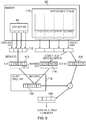
- FIG. 1 schematically illustrates a data processing apparatus 10 which may embody various examples of the present techniques.
- the apparatus comprises data processing circuitry 12 which performs data processing operations on data items in response to a sequence of instructions which it executes. These instructions are retrieved from the memory 14 to which the data processing apparatus has access and, in a manner with which one of ordinary skill in the art will be familiar, fetch circuitry 16 is provided for this purpose. Furthermore, instructions retrieved by the fetch circuitry 16 are passed to the instruction decoder circuitry 18, which generates control signals which are arranged to control various aspects of the configuration and operation of the processing circuitry 12, as well as of a set of registers 20 and a load/store unit 22.
- the data processing circuitry 12 may be arranged in a pipelined fashion, yet the specifics thereof are not relevant to the present techniques.
- the registers 20, as can be seen in Figure 1 each comprise storage for multiple data elements, such that the processing circuitry can apply data processing operations either to a specified data element within a specified register, or can apply data processing operations to a specified group of data elements (a "vector") within a specified register.
- the illustrated data processing apparatus is concerned with the performance of counting operations with respect to data elements held in the registers 20, further explanation of which will follow in more detail below with reference to some specific embodiments.
- Data values required by the data processing circuitry 12 in the execution of the instructions, and data values generated as a result of those data processing instructions, are written to and read from the memory 14 by means of the load/store unit 22.
- the memory 14 in Figure 1 can be seen as an example of a computer-readable storage medium on which the instructions of the present techniques can be stored, typically as part of a predefined sequence of instructions (a "program"), which the processing circuitry then executes.
- the processing circuitry may however access such a program from a variety of different sources, such in RAM, in ROM, via a network interface, and so on.
- the present disclosure describes various novel instructions which the processing circuitry 12 can execute and the figures which follow provide further explanation of the nature of these instructions, variations in the data processing circuitry in order to support the execution of those instructions, and so on.
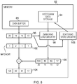
- FIG. 2 schematically illustrates some more detail of the components of a data processing apparatus in one embodiment.
- the data processing circuitry 30 of Figure 2 is shown comprising some specific components, namely the counting circuitry 32, the summing circuitry 34, the register gather and scatter circuitry 36, and the gather index generation circuitry 38. As illustrated in the figure, these items of circuitry have access to the registers of the set of registers 40, where this access is under the control of the control signals generated by the instruction decoder circuitry 42.
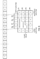
- Figure 3 is an illustration of an input data vector to graphically show some terminology used in this description, wherein it can be seen the input data vector comprises a plurality of segments, and wherein each segment comprises a plurality of input elements. In the example shown, each segment comprises 4 input elements. Hence for example, where the input data vector corresponds to the full content of a 512-bit vector register, this content may be treated in four 128-bit segments, each of which comprises four 32-bit values (input elements).
- Figure 4 schematically illustrates a count operation performed by data processing circuitry in one embodiment.
- an input data item is shown comprising a subset (substring) of the input data item.
- a reference data item comprising a plurality of reference elements each containing a reference value.
- a count value is determined by comparing each reference value in a respective reference element of the reference data item with each input element of the subset. Depending on the implementation this may be sequential or parallelised. Referring to the example shown, when the first reference element of the reference data item, containing the reference value "0”, is compared with the first input element of the subset, containing the input value "0", the comparison is a match.
- Figure 5 illustrates the behaviour of a plurality of count operations according to one example to determine a count data item corresponding to a reference data item and a subset of an input data item.
- the subset of elements in the specified input data item is a segment thereof, and in here the input data item is illustrated containing the set of input values [4 2 2 0] and a reference data item comprising a set of 4 reference values is shown which have the reference values [0 1 2 3].
- the count operation as described previously with reference to Figure 4 is performed for each reference value in a respective reference element of the reference data item. In respect of the second reference element with the reference value "1", since there are no input elements with an input value of "1" in the subset, the count value for that reference element is "0".
- each count value indicates the number of input elements which contain an input value which matches the respective reference value.
- This set of operations shown are carried out in some embodiments in response to a "match segment” instruction (also referred to herein as "MATCHSEG") as will be described further below.
- the counting circuitry (item 32 in Figure 2 ) provided to support these operations essentially comprises a matrix of sixteen comparators (corresponding to the central 4x4 grid in Figure 5 ), such that comparisons between any of the input data item elements can be made with any of the reference data item elements, with the cumulative results of a row of comparators providing the count values illustrated in the left-most column (i.e. the count data item).
- Figure 6 illustrates the behaviour of a plurality of count operations according to one example to determine a count data item corresponding to a reference data item and a subset of an input data item.
- the subset of elements in the specified input data item used by each successive count operation is shown to vary between the count operations.
- a plurality of reference elements in a reference data item includes a first reference element 71, a second reference element 72, a third reference element 73, and a fourth reference element 74.
- a plurality of input elements are illustrated in an input data item, including a first input element 75, second input element 76, a third input element 77, and a fourth input element 78.
- the input data item and the reference data item have a one-to-one correspondence in this example, i.e. they are identical.
- the first count operation corresponding to the first reference element 71 uses a subset of elements in the specified input data item comprising only the first input element (containing the value "0").
- the range of reference elements is adjusted based on the position of the respective element used by a respective count operation. For example, the count operation corresponding to the third reference element 73 with a reference value "2" counts the number of input elements in the subset of elements in the specified input data item bounded by the third input element 77. Accordingly, the range of element positions is bounded by the respective reference element used in each of the plurality of count operations.
- This approach where the input data item and the reference data item are the same, enables an counting operation to be carried out to determine the number of instances of each input data item value within that input data item.
- the incrementing set of comparisons made enables redundant comparisons to be avoided and an efficient determination of the required "number of instances" to be carried out.
- the operations shown provide a mechanism via which the apparatus can disambiguate (rationalise) the input data items so that correct access to those storage locations is made.
- the identification of multiple instances of a given index in the input data item enables the apparatus to ensure that accesses to the given index of the stored histogram are correctly carried out (e.g. by strict preservation of index ordering).
- the set of operations shown are carried out in some embodiments in response to a "match count” instruction (also referred to herein as "MATCHCNT") as will be described further below.
- the counting circuitry (item 32 in Figure 2 ) provided to support these operations may also comprise a matrix of sixteen comparators (corresponding to the central 4x4 grid in Figure 5 ).
- Histogram processing can be relevant to a range of applications such as in graphics processing, in computer vision processing, in server processing tasks such as sorting, and in many other high-performance computing contexts.
- One notable parameter which can significantly influence how the histogram processing is carried out is the size of the histogram.
- size of the histogram refers in particular to the "width" of the histogram in the sense of the number of distinct bins which it comprises.
- the size of the data which must be represented in each bin of course also contributes to the overall size of the histogram.
- a histogram with a relatively modest width may nonetheless require significant storage capacity if each of its bins is required to store large values. Equally a histogram with a large number of bins may nonetheless only require modest storage capacity if each of its bins is only required to store small values.
- the present techniques recognise that where the histogram is particularly large it may only be practical for the histogram entries to be stored in memory, and for updates to the histogram to be carried out by means of targeted memory accesses. For example rather than frequently retrieving, modifying and rewriting large sections of the histogram, gathering loads from memory and scattering stores to memory may be used to access and modify specific histogram entries.
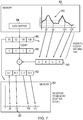
- Figure 7 schematically illustrates data processing being performed with respect to a large histogram 80, which is stored in a memory 82. It will of course be appreciated that what is actually stored within the memory 82 is a large set of data values, each representative of the frequency count for each bin of the histogram 80, but a graphical representation thereof is shown in Figure 7 for ease of visual recognition. Also shown to be stored in the memory 82 is data buffer 84 which temporarily holds data values for accumulation in the histogram. These data values for updating the histogram need not necessarily be retrieved from memory, and could for example result from other processing of data values in registers of the apparatus. Figure 7 illustrates the data processing to enable this accumulation to take place.
- a data item 86 is received from the data buffer 84 and is the subject of a count operation to generate the set of count values 88 which should be added to the respective histogram bins.
- the data item 86 also controls the operation of a memory-to-register gathering load, by means of which the histogram entries (bin counts held at specific storage locations) for the set of four indices forming the data item 86 are loaded as set of data values 90 into a register.
- the set of count values 88 and the set of data values 90 are then summed (in summing circuitry) to generate an updated set of histogram entries 92.
- FIG 8 schematically illustrates an example of the histogram processing discussed with reference to Figure 7 , where a "MATCHCNT" instruction of the present techniques is used to perform the counting step.
- Histogram data storage 94 is shown in memory 82 (in which a large histogram 80 is stored).
- An input data item 96 is received from the data buffer 84, which is subjected to the MATCHCNT instruction and also forms an input to the gathering load circuitry 98.
- the gathering load circuitry 98 retrieves the set of specified histogram entries 100 from the specified bins of the histogram.
- the MATCHCNT instruction generates the count vector 102.
- the count of "1" for the first instance of 15 is superseded by the second count of "2".
- the set of count values 102 and the set of data values 100 are then summed (in summing circuitry) to generate an updated set of histogram entries 104.
- This is then the subject of a register-to-memory scattering store, performed by the scattering store circuitry 106 (also controlled by the data item 96), such that the updated set of histogram entries 104 is stored back into the specified histogram entries (bin counts held at specific storage locations) in memory 82.
- the scattering store circuitry 106 (and any other components - not explicitly illustrated - involved in such a memory access) are configured to strictly respect the above-mentioned ordering of proceeding from least significant to most significant indices of a vector to ensure that the incorrect (or at least incomplete) histogram update of 81 is superseded or overwritten by the correct histogram update of 82 in the storage location corresponding to histogram index 15.
- Figure 9 schematically illustrates data processing being performed with respect to a "medium sized" histogram stored in histogram storage 110 of memory 82.
- a histogram of relatively limited width is shown, having 16 bins.
- Figure 9 illustrates a different approach to the data processing (to that of Figures 7 and 8 ) to enable the accumulation into the histogram to take place.
- the data item 112 is loaded from the data buffer 84 (as a contiguous load) and this is transferre to represent a set of "keys" (i.e. histogram bins) 113.
- a load takes place to retrieve a first portion of the histogram content (e.g. bins 12-15, as illustrated) from memory.
- This provides two further items used in the processing, namely the set of reference keys 114 and the content of that portion of the histogram content 116.
- the input data keys 113 and the reference keys 114 form the two inputs to a count operation triggered by the MATCHSEG instruction in the count circuitry 118 (item 32 in Figure 2 ).
- the input data item 112 can be copied (replicated) one or more times in providing the set of keys 113, such that the full parallel counting capacity is used.
- FIG 10 schematically illustrates data processing being performed with respect to a histogram which is small enough to be stored in the registers of the apparatus. Illustrated are four vector registers 130, 131, 132, and 133. The respective elements of each of these vector registers hold histogram bin entries across 32 bins.
- An input data item 140 is subjected to the MATCHCNT operation (in count circuitry 142) and also forms an input to the gathering register lookup (TBL) instruction.
- the TBL causes register gather circuitry (item 36 in Figure 2 ) to retrieves a set of specified histogram entries 146 (also referred to as a current sum vector) from the specified, non-contiguous vector register elements (bins of the histogram).
- the MATCHCNT operation generates the count vector 148 and this is summed with the current sum vector 146 to generate a resultant data item 150.
- This is then the subject of a scattering register store, performed by the register scatter circuitry 106 (item 36 in Figure 2 ) to cause the updated set of histogram entries to be stored back to the from the non-contiguous vector register elements (bins of the histogram) specified by the input data item.
- a scattering register store is initiated by the instruction STB (Store-to-table), although in this particular example a variant thereon, STBX, is used since the scatter spans multiple registers. Note that when (as shown in the example of Figure 10 ) there is a repeated index in the input data item (i.e. 15), the scattering register store must respect the right-to-left (least significant to most significant index) of the input data item indices to ensure that the correct updated histogram entry (B+2) is not corrupted by an earlier incorrect update (B+1).
- Figure 11 schematically illustrates data processing being performed with respect to the same histogram as shown in Figure 10 , i.e. stored across four vector registers 130, 131, 132, and 133.
- the histogram is deemed to be small enough that a contiguous access approach is taken, in which the content of each vector register is accessed as a contiguous unit 162 in turn, updated as necessary based on the input data item, and returned to the respective vector register.
- the capacity of the MATCHSEG operation is for a reference data item which is half a vector register length
- the content of each accessed vector register is also iteratively processed in two portions (halves).
- the input data item 160 is subjected to the MATCHSEG operation (in count circuitry 142) with the respective portion of the current vector register content 162 forming the reference input.
- the MATCHSEG operation generates the count vector 164 and this is summed with the current portion of the vector register content 162 to generate a resultant data item 166. Once completed by the other portion, this is stored in the relevant vector register of vector registers 130, 131, 132, and 133.
- Figure 12 illustrates a gather index generation operation performed by gather index generation circuitry (e.g. item 38 in Figure 2 ) in response to a GENIDX instruction in one embodiment.
- a scatter index 180 is provided which comprises the scatter elements [2 3 0 3] and the gather index generation instruction (GENIDX) causes the generation of the gather index 182 illustrated.
- GENIDX gather index generation instruction
- FIG. 13 is a flow diagram showing the steps which are taken when generating a gather index from a scatter index in one example.
- the flow begins at step 200 with a GENIDX instruction which specifies a scatter index and the destination into which the generated gather index should be created.
- An outer loop is initiated at step 202 to loop over all element IDs in the gather index array to be generated.
- An inner loop is initiated at step 204 to loop over all element IDs of the scatter index being processed.
- it is determined if the value stored in the current scatter index element i.e. the value stored, not the ID of the element
- the flow proceeds via step 208, where the current gather index element is populated with that scatter index element ID. If it does not, the flow proceeds directly to step 210, which continues the loop over scatter index element IDs. Thereafter step 212 continues the loop over gather index element IDs.
- the flow concludes at step 214 and the gather index generation is complete.
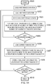
- Figure 14 illustrates a flow diagram illustrating the method of operating an apparatus according to one example.
- the process begins at step 1000.
- a reference data item is loaded at step 1001.
- a first (next) input data item is loaded at step 1002.
- the process continues by selecting the next reference element at step 1003.
- a count operation is performed to determine a count value indicative of a number of times the reference value matches a respective value in each input element of a subset of elements in the specified input data item.
- Step 1005 determines whether the current reference element is the last reference element. If it is not, steps 1003-1004 are repeated until the condition in step 1005 is met.
- step 1005 If the condition in step 1005 is met, the current sum vector is loaded 1006 and at step 1007 a summing operation is performed which adds the value of each count element to the value stored in the corresponding element of the current sum vector.
- step 1008 the resultant data item is stored at the location of the current sum vector.
- step 1009 it is determined whether the input data item which steps 1002 to 1008 used is the last input data item to be processed in the input vector. If the condition in step 1009 is not met, steps 1002 to 1008 are repeated. If the condition of step 1009 is met, then the method finishes at step 1010.
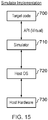
- FIG 15 illustrates a simulator implementation that may be used. Whilst the earlier described embodiments implement the present invention in terms of apparatus and methods for operating specific processing hardware supporting the techniques concerned, it is also possible to provide an instruction execution environment in accordance with the embodiments described herein which is implemented through the use of a computer program. Such computer programs are often referred to as simulators, insofar as they provide a software based implementation of a hardware architecture. Varieties of simulator computer programs include emulators, virtual machines, models, and binary translators, including dynamic binary translators. Typically, a simulator implementation may run on a host processor 730, optionally running a host operating system 720, supporting the simulator program 710.
- the hardware there may be multiple layers of simulation between the hardware and the provided instruction execution environment, and/or multiple distinct instruction execution environments provided on the same host processor.
- powerful processors have been required to provide simulator implementations which execute at a reasonable speed, but such an approach may be justified in certain circumstances, such as when there is a desire to run code native to another processor for compatibility or re-use reasons.
- the simulator implementation may provide an instruction execution environment with additional functionality which is not supported by the host processor hardware, or provide an instruction execution environment typically associated with a different hardware architecture.
- An overview of simulation is given in " Some Efficient Architecture Simulation Techniques", Robert Bedichek, Winter 1990 USENIX Conference, Pages 53 - 63 .
- the simulator program 710 may be stored on a computer-readable storage medium (which may be a non-transitory medium), and provides a program interface (instruction execution environment) to the target code 700 (which may include the applications, operating systems and a hypervisor as shown in Figure 2 ) which is the same as the application program interface of the hardware architecture being modelled by the simulator program 710.
- the program instructions of the target code 700 including the count instructions, register scatter storage instructions, and the gather index generation instructions described above, may be executed from within the instruction execution environment using the simulator program 710, so that a host computer 730 which does not actually have the hardware features of the apparatus 2 discussed above can emulate these features.
- Instruction decoder circuitry is responsive to a count instruction specifying an input data item to generate control signals to control the data processing circuitry to perform a count operation.
- the count operation determines a count value indicative of a number of input elements of a subset of elements in the specified input data item which have a value which matches a reference value in a reference element in a reference data item.
- a plurality of count operations may be performed to determine a count data item corresponding to the input data item.
- a register scatter storage instruction, a gather index generation instruction, and respective apparatuses responsive to them, as well as simulator implementations, are also provided.
- the words “configured to" are used to mean that an element of an apparatus has a configuration able to carry out the defined operation.
- a “configuration” means an arrangement or manner of interconnection of hardware or software.
- the apparatus may have dedicated hardware which provides the defined operation, or a processor or other processing device may be programmed to perform the function.
- Configured to does not imply that the apparatus element needs to be changed in any way in order to provide the defined operation.
Landscapes
- Engineering & Computer Science (AREA)
- Software Systems (AREA)
- Theoretical Computer Science (AREA)
- Physics & Mathematics (AREA)
- General Engineering & Computer Science (AREA)
- General Physics & Mathematics (AREA)
- Mathematical Physics (AREA)
- Complex Calculations (AREA)
- Advance Control (AREA)
- Executing Machine-Instructions (AREA)
- Investigating Or Analysing Biological Materials (AREA)
- Radar Systems Or Details Thereof (AREA)
Claims (14)
- Vorrichtung, umfassend:Anweisungsdecoder-Schaltung zum Decodieren von Anweisungen; undeine Datenverarbeitungsschaltung zum selektiven Anwenden von durch die Anweisungen vorgegebenen Vektorverarbeitungsoperationen auf einen Eingabedatenvektor, der mehrere Eingabedatenelemente an jeweiligen Positionen im Eingabedatenvektor umfasst,wobei die Anweisungsdecoder-Schaltung auf eine Zählanweisung reagiert, die ein Eingabedatenelement vorgibt, um Steuersignale zum Steuern der Datenverarbeitungsschaltung zu erzeugen, um:eine Zähloperation zum Bestimmen eines Zählwerts durchzuführen, der für eine Anzahl von Eingabeelementen einer Teilmenge von Elementen in dem vorgegebenen Eingabedatenelement kennzeichnend ist, die einen Wert haben, der mit einem Referenzwert in einem Referenzelement in einem Referenzdatenelement übereinstimmt,wobei die Datenverarbeitungsschaltung ferner auf die Steuersignale reagiert, um mehrere Zähloperationen durchzuführen,wobei in jeder der mehreren Zähloperationen der verwendete Referenzwert ein jeweiliger Referenzwert in einem jeweiligen Referenzelement mehrerer Referenzelemente in dem Referenzdatenelement ist,wobei die Teilmenge von Elementen in dem vorgegebenen Eingabedatenelement jedes Eingabeelement des Eingabedatenelements umfasst, das eine Elementposition in dem Eingabedatenelement aufweist, die innerhalb eines Bereichs von Elementpositionen in dem Eingabedatenelement liegt, undwobei der Bereich der Elementpositionen durch das jeweilige Referenzelement begrenzt ist, das in jeder der mehreren Zähloperationen verwendet wird.
- Vorrichtung nach Anspruch 1, wobei die Datenverarbeitungsschaltung auf die Steuersignale für jede der mehreren Zähloperationen reagiert, um den Zählwert in einem jeweiligen Zählelement eines Zähldatenelements einzustellen, um den durch diese Zähloperation bestimmten Zählwert anzugeben.
- Vorrichtung nach Anspruch 1, wobei der Bereich der Elementpositionen die jeweiligen Referenzelemente umfasst, die in jeder vorhergehenden Zähloperation der mehreren Zähloperationen verwendet werden.
- Vorrichtung nach einem der Ansprüche 1-3, wobei die Datenverarbeitungsschaltung auf die Steuersignale reagiert, um die mehreren Zähloperationen in einer aufsteigenden Reihenfolge der Elementpositionen von den niedrigstwertigen Elementpositionen zu den höchstwertigen Elementpositionen durchzuführen.
- Vorrichtung nach einem der Ansprüche 1-4, wobei der Referenzwert in jedem Referenzelement des Referenzdatenelements durch den Eingabewert in jedem entsprechenden Eingabeelement des Eingabedatenelements bereitgestellt wird.
- Vorrichtung nach einem der Ansprüche 1-5, wobei das Eingabedatenelement ein oder mehrere Segmente umfasst, wobei jedes Segment eine vordefinierte Größe hat und die Teilmenge ein ausgewähltes Segment des einen oder der mehreren Segmente ist.
- Vorrichtung nach den Ansprüchen 1-6, wobei das Eingabedatenelement ein oder mehrere Segmente umfasst, wobei jedes Segment eine vordefinierte Größe hat und die Teilmenge ein ausgewähltes Segment des einen oder der mehreren Segmente ist,
und wobei die Teilmenge das ausgewählte Segment für jede Zähloperation der mehreren Zähloperationen ist. - Vorrichtung nach Anspruch 6 oder Anspruch 7, wenn abhängig von Anspruch 6, wobei die Datenverarbeitungsschaltung ferner auf die Steuersignale reagiert, um mehrere Zähloperationen durchzuführen,wobei in jeder der mehreren Zähloperationen der verwendete Referenzwert ein jeweiliger Referenzwert in einem jeweiligen Referenzelement mehrerer Referenzelemente in dem Referenzdatenelement ist,wobei die Datenverarbeitungsschaltung ferner eine Eingabedatenelement-Kopierschaltung umfasst, um eine Kopie des ausgewählten Segments des Eingabedatenelements zu erzeugen,und die Datenverarbeitungsschaltung auf die Steuersignale reagiert, um eine erste Gruppe der mehreren Zähloperationen unter Bezugnahme auf das ausgewählte Segment des Eingabedatenelements durchzuführen und um eine zweite Gruppe der mehreren Zähloperationen unter Bezugnahme auf die Kopie des ausgewählten Segments des Eingabedatenelements durchzuführen.
- Vorrichtung nach Anspruch 6 oder einem der Ansprüche 7-8, wenn abhängig von Anspruch 6, wobei die mehreren Referenzelemente in dem Referenzdatenelement aus dem Speicher in einer zusammenhängenden Last abgerufen werden.
- Vorrichtung nach Anspruch 2 oder nach einem der Ansprüche 3-9, wenn abhängig von Anspruch 2, wobei die Datenverarbeitungsschaltung ferner eine Summierschaltung umfasst, um eine Summieroperation durchzuführen, und die Anweisungsdecoder-Schaltung auf eine Summieranweisung reagiert, die einen aktuellen Summenvektor vorgibt, um die Summierschaltung zu steuern, um eine Summieroperation unter Verwendung des aktuellen Summenvektors durchzuführen, um den Wert jedes Zählelements im Zähldatenelement zu dem Wert im entsprechenden Element des aktuellen Summenvektors zu addieren und ein resultierendes Datenelement auszugeben.
- Vorrichtung nach Anspruch 10, wobei die Summierungsoperation nach Abschluss der mehreren Zähloperationen durchgeführt wird.
- Verfahren zum Betreiben einer Vorrichtung zur Datenverarbeitung, das die folgenden Schritte umfasst:Decodieren von Anweisungen;selektives Anwenden von durch die Anweisungen vorgegebenen Verarbeitungsoperationen auf einen Eingabedatenvektor, der mehrere Eingabedatenelemente an jeweiligen Positionen in dem Eingabedatenvektor umfasst; undErzeugen von Steuersignalen als Reaktion auf eine Zählanweisung, die ein Eingabedatenelement vorgibt, um eine Datenverarbeitungsschaltung zu steuern, um:mehrere Zähloperationen durchzuführen, wobei jede der mehreren Zähloperationen dazu dient, einen Zählwert zu bestimmen, der für eine Anzahl von Eingabeelementen einer Teilmenge von Elementen in dem vorgegebenen Eingabedatenelement kennzeichnend ist, die einen Wert aufweisen, der mit einem jeweiligen Referenzwert in einem jeweiligen Referenzelement in mehreren Referenzelementen in einem Referenzdatenelement übereinstimmt,wobei die Teilmenge von Elementen in dem vorgegebenen Eingabedatenelement jedes Eingabeelement des Eingabedatenelements umfasst, das eine Elementposition in dem Eingabedatenelement aufweist, die innerhalb eines Bereichs von Elementpositionen in dem Eingabedatenelement liegt, undwobei der Bereich der Elementpositionen durch das jeweilige Referenzelement begrenzt ist, das in jeder der mehreren Zähloperationen verwendet wird.
- Computerprogramm zum Steuern einer Host-Datenverarbeitungsvorrichtung nach Anspruch 1, um eine Anweisungsausführungsumgebung bereitzustellen, umfassend:Anweisungsdecodierungs-Programmlogik zum Decodieren von Anweisungen; undDatenverarbeitungsprogrammlogik, um selektiv durch die Anweisungen vorgegebene Verarbeitungsoperationen auf eine Eingabedaten-Vektorstruktur anzuwenden, die mehrere Eingabedatenelementstrukturen an jeweiligen Positionen in der Eingabedaten-Vektorstruktur umfasst,wobei die Anweisungsdecodierungs-Programmlogik auf eine Zählanweisung reagiert, die eine Eingabedatenelementstruktur vorgibt, um Steuersignale zum Steuern der Datenverarbeitungsprogrammlogik zu erzeugen, um:mehrere Zähloperationen durchzuführen, wobei jede der mehreren Zähloperationen dazu dient, einen Zählwert zu bestimmen, der für eine Anzahl von Eingabeelementen einer Teilmenge von Elementen in der vorgegebenen Eingabedatenelementstruktur kennzeichnend ist, die einen Wert aufweisen, der mit einem jeweiligen Referenzwert in einem jeweiligen Referenzelement in mehreren Referenzelementen in einer Referenzdatenelement-Struktur übereinstimmt,wobei die Teilmenge von Elementen in der vorgegebenen Eingabedatenelementstruktur jedes Eingabeelement der Eingabedatenelementstruktur umfasst, das eine Elementposition in der Eingabedatenelementstruktur aufweist, die innerhalb eines Bereichs von Elementpositionen in der Eingabedatenelementstruktur liegt, undwobei der Bereich der Elementpositionen durch das jeweilige Referenzelement begrenzt ist, das in jeder der mehreren Zähloperationen verwendet wird.
- Computerlesbarer Datenträger, auf dem das Computerprogramm nach Anspruch 13 gespeichert ist.
Applications Claiming Priority (2)
| Application Number | Priority Date | Filing Date | Title |
|---|---|---|---|
| US15/665,781 US11042375B2 (en) | 2017-08-01 | 2017-08-01 | Counting elements in data items in a data processing apparatus |
| PCT/GB2018/052001 WO2019025754A1 (en) | 2017-08-01 | 2018-07-13 | COUNTING ELEMENTS IN DATA ELEMENTS IN A DATA PROCESSING APPARATUS |
Publications (2)
| Publication Number | Publication Date |
|---|---|
| EP3662365A1 EP3662365A1 (de) | 2020-06-10 |
| EP3662365B1 true EP3662365B1 (de) | 2021-09-22 |
Family
ID=63143266
Family Applications (1)
| Application Number | Title | Priority Date | Filing Date |
|---|---|---|---|
| EP18752198.4A Active EP3662365B1 (de) | 2017-08-01 | 2018-07-13 | Zählen von elementen in datenobjekten in einer datenverarbeitungsvorrichtung |
Country Status (7)
| Country | Link |
|---|---|
| US (1) | US11042375B2 (de) |
| EP (1) | EP3662365B1 (de) |
| JP (1) | JP7335225B2 (de) |
| KR (1) | KR102594768B1 (de) |
| CN (1) | CN110945477B (de) |
| TW (1) | TWI787313B (de) |
| WO (1) | WO2019025754A1 (de) |
Families Citing this family (12)
| Publication number | Priority date | Publication date | Assignee | Title |
|---|---|---|---|---|
| US10817297B2 (en) * | 2019-03-30 | 2020-10-27 | Intel Corporation | Method and apparatus for vector-matrix comparison |
| US11340904B2 (en) | 2019-05-20 | 2022-05-24 | Micron Technology, Inc. | Vector index registers |
| US11403256B2 (en) | 2019-05-20 | 2022-08-02 | Micron Technology, Inc. | Conditional operations in a vector processor having true and false vector index registers |
| US11507374B2 (en) * | 2019-05-20 | 2022-11-22 | Micron Technology, Inc. | True/false vector index registers and methods of populating thereof |
| US11327862B2 (en) | 2019-05-20 | 2022-05-10 | Micron Technology, Inc. | Multi-lane solutions for addressing vector elements using vector index registers |
| US11321051B2 (en) * | 2019-05-21 | 2022-05-03 | Arm Limited | Statistical mode determination |
| WO2021026225A1 (en) * | 2019-08-08 | 2021-02-11 | Neuralmagic Inc. | System and method of accelerating execution of a neural network |
| US11366811B2 (en) * | 2020-05-21 | 2022-06-21 | Sap Se | Data imprints techniques for use with data retrieval methods |
| CN114691560B (zh) * | 2020-12-25 | 2025-10-17 | 安徽寒武纪信息科技有限公司 | 数据处理电路、数据处理方法及相关产品 |
| US11860780B2 (en) | 2022-01-28 | 2024-01-02 | Pure Storage, Inc. | Storage cache management |
| US20240403052A1 (en) * | 2023-06-05 | 2024-12-05 | Arm Limited | Indexed vector permutation operations |
| US12405898B1 (en) * | 2024-02-26 | 2025-09-02 | Arm Limited | Memory synchronisation subsequent to a page table walk |
Family Cites Families (20)
| Publication number | Priority date | Publication date | Assignee | Title |
|---|---|---|---|---|
| US4307377A (en) | 1979-11-09 | 1981-12-22 | Bell Telephone Laboratories, Incorporated | Vector coding of computer graphics material |
| US4991134A (en) | 1988-03-30 | 1991-02-05 | International Business Machines Corporation | Concurrent sorting apparatus and method using FIFO stacks |
| US5608662A (en) | 1995-01-12 | 1997-03-04 | Television Computer, Inc. | Packet filter engine |
| US6789116B1 (en) | 1999-06-30 | 2004-09-07 | Hi/Fn, Inc. | State processor for pattern matching in a network monitor device |
| US6665790B1 (en) | 2000-02-29 | 2003-12-16 | International Business Machines Corporation | Vector register file with arbitrary vector addressing |
| GB0210604D0 (en) | 2002-05-09 | 2002-06-19 | Ibm | Method and arrangement for data compression |
| US20050086234A1 (en) | 2003-10-15 | 2005-04-21 | Sierra Wireless, Inc., A Canadian Corporation | Incremental search of keyword strings |
| GB2411975B (en) | 2003-12-09 | 2006-10-04 | Advanced Risc Mach Ltd | Data processing apparatus and method for performing arithmetic operations in SIMD data processing |
| US7130983B1 (en) * | 2003-12-17 | 2006-10-31 | Storage Technology Corporation | System and method for reference count regeneration |
| US20060149938A1 (en) | 2004-12-29 | 2006-07-06 | Hong Jiang | Determining a register file region based at least in part on a value in an index register |
| US9513905B2 (en) * | 2008-03-28 | 2016-12-06 | Intel Corporation | Vector instructions to enable efficient synchronization and parallel reduction operations |
| US7908457B2 (en) | 2008-05-05 | 2011-03-15 | International Business Machines Corporation | Retaining an association between a virtual address based buffer and a user space application that owns the buffer |
| GB2464292A (en) * | 2008-10-08 | 2010-04-14 | Advanced Risc Mach Ltd | SIMD processor circuit for performing iterative SIMD multiply-accumulate operations |
| CN106293631B (zh) * | 2011-09-26 | 2020-04-10 | 英特尔公司 | 用于提供向量分散操作和聚集操作功能的指令和逻辑 |
| CN104303142B (zh) * | 2012-06-02 | 2019-03-08 | 英特尔公司 | 使用索引阵列和有限状态机的分散 |
| US20140188961A1 (en) * | 2012-12-27 | 2014-07-03 | Mikhail Plotnikov | Vectorization Of Collapsed Multi-Nested Loops |
| US9804839B2 (en) * | 2012-12-28 | 2017-10-31 | Intel Corporation | Instruction for determining histograms |
| US9424031B2 (en) | 2013-03-13 | 2016-08-23 | Intel Corporation | Techniques for enabling bit-parallel wide string matching with a SIMD register |
| US9513907B2 (en) * | 2013-08-06 | 2016-12-06 | Intel Corporation | Methods, apparatus, instructions and logic to provide vector population count functionality |
| US9396056B2 (en) * | 2014-03-15 | 2016-07-19 | Intel Corporation | Conditional memory fault assist suppression |
-
2017
- 2017-08-01 US US15/665,781 patent/US11042375B2/en active Active
-
2018
- 2018-07-13 JP JP2020504004A patent/JP7335225B2/ja active Active
- 2018-07-13 CN CN201880049811.7A patent/CN110945477B/zh active Active
- 2018-07-13 WO PCT/GB2018/052001 patent/WO2019025754A1/en not_active Ceased
- 2018-07-13 EP EP18752198.4A patent/EP3662365B1/de active Active
- 2018-07-13 KR KR1020207004946A patent/KR102594768B1/ko active Active
- 2018-07-31 TW TW107126469A patent/TWI787313B/zh active
Also Published As
| Publication number | Publication date |
|---|---|
| KR20200031150A (ko) | 2020-03-23 |
| JP7335225B2 (ja) | 2023-08-29 |
| US11042375B2 (en) | 2021-06-22 |
| US20190042253A1 (en) | 2019-02-07 |
| TW201911034A (zh) | 2019-03-16 |
| KR102594768B1 (ko) | 2023-10-27 |
| EP3662365A1 (de) | 2020-06-10 |
| JP2020529658A (ja) | 2020-10-08 |
| CN110945477B (zh) | 2023-10-20 |
| CN110945477A (zh) | 2020-03-31 |
| WO2019025754A1 (en) | 2019-02-07 |
| TWI787313B (zh) | 2022-12-21 |
Similar Documents
| Publication | Publication Date | Title |
|---|---|---|
| EP3662365B1 (de) | Zählen von elementen in datenobjekten in einer datenverarbeitungsvorrichtung | |
| JP6843187B2 (ja) | ダブルロード命令 | |
| IL271438B1 (en) | Checking bit values inside vector elements | |
| EP3759592B1 (de) | Datenverarbeitung | |
| JP7245817B2 (ja) | データ処理装置における連続値の照合 | |
| US12360767B2 (en) | Data processing apparatus, method and virtual machine | |
| US20210334102A1 (en) | Generating a vector predicate summary | |
| US12493665B2 (en) | Device and method for operation of data | |
| US12504973B2 (en) | Technique for handling data elements stored in an array storage | |
| JP2024525798A (ja) | 述語技術 | |
| KR20250002372A (ko) | 어레이 저장소에 저장되는 데이터 요소를 핸들링하기 위한 기술 | |
| GB2630328A (en) | Methods and systems for data transfer | |
| WO2025210334A1 (en) | Vector cryptographic processing | |
| KR20250020652A (ko) | 외적 연산을 수행하기 위한 기술 | |
| JPS6313216B2 (de) |
Legal Events
| Date | Code | Title | Description |
|---|---|---|---|
| STAA | Information on the status of an ep patent application or granted ep patent |
Free format text: STATUS: UNKNOWN |
|
| STAA | Information on the status of an ep patent application or granted ep patent |
Free format text: STATUS: THE INTERNATIONAL PUBLICATION HAS BEEN MADE |
|
| PUAI | Public reference made under article 153(3) epc to a published international application that has entered the european phase |
Free format text: ORIGINAL CODE: 0009012 |
|
| STAA | Information on the status of an ep patent application or granted ep patent |
Free format text: STATUS: REQUEST FOR EXAMINATION WAS MADE |
|
| 17P | Request for examination filed |
Effective date: 20200216 |
|
| AK | Designated contracting states |
Kind code of ref document: A1 Designated state(s): AL AT BE BG CH CY CZ DE DK EE ES FI FR GB GR HR HU IE IS IT LI LT LU LV MC MK MT NL NO PL PT RO RS SE SI SK SM TR |
|
| AX | Request for extension of the european patent |
Extension state: BA ME |
|
| DAV | Request for validation of the european patent (deleted) | ||
| DAX | Request for extension of the european patent (deleted) | ||
| GRAP | Despatch of communication of intention to grant a patent |
Free format text: ORIGINAL CODE: EPIDOSNIGR1 |
|
| STAA | Information on the status of an ep patent application or granted ep patent |
Free format text: STATUS: GRANT OF PATENT IS INTENDED |
|
| INTG | Intention to grant announced |
Effective date: 20210420 |
|
| GRAS | Grant fee paid |
Free format text: ORIGINAL CODE: EPIDOSNIGR3 |
|
| GRAA | (expected) grant |
Free format text: ORIGINAL CODE: 0009210 |
|
| STAA | Information on the status of an ep patent application or granted ep patent |
Free format text: STATUS: THE PATENT HAS BEEN GRANTED |
|
| AK | Designated contracting states |
Kind code of ref document: B1 Designated state(s): AL AT BE BG CH CY CZ DE DK EE ES FI FR GB GR HR HU IE IS IT LI LT LU LV MC MK MT NL NO PL PT RO RS SE SI SK SM TR |
|
| REG | Reference to a national code |
Ref country code: GB Ref legal event code: FG4D |
|
| REG | Reference to a national code |
Ref country code: IE Ref legal event code: FG4D |
|
| REG | Reference to a national code |
Ref country code: DE Ref legal event code: R096 Ref document number: 602018023955 Country of ref document: DE |
|
| REG | Reference to a national code |
Ref country code: CH Ref legal event code: EP Ref country code: AT Ref legal event code: REF Ref document number: 1432851 Country of ref document: AT Kind code of ref document: T Effective date: 20211015 |
|
| REG | Reference to a national code |
Ref country code: LT Ref legal event code: MG9D |
|
| REG | Reference to a national code |
Ref country code: NL Ref legal event code: MP Effective date: 20210922 |
|
| PG25 | Lapsed in a contracting state [announced via postgrant information from national office to epo] |
Ref country code: RS Free format text: LAPSE BECAUSE OF FAILURE TO SUBMIT A TRANSLATION OF THE DESCRIPTION OR TO PAY THE FEE WITHIN THE PRESCRIBED TIME-LIMIT Effective date: 20210922 Ref country code: SE Free format text: LAPSE BECAUSE OF FAILURE TO SUBMIT A TRANSLATION OF THE DESCRIPTION OR TO PAY THE FEE WITHIN THE PRESCRIBED TIME-LIMIT Effective date: 20210922 Ref country code: FI Free format text: LAPSE BECAUSE OF FAILURE TO SUBMIT A TRANSLATION OF THE DESCRIPTION OR TO PAY THE FEE WITHIN THE PRESCRIBED TIME-LIMIT Effective date: 20210922 Ref country code: HR Free format text: LAPSE BECAUSE OF FAILURE TO SUBMIT A TRANSLATION OF THE DESCRIPTION OR TO PAY THE FEE WITHIN THE PRESCRIBED TIME-LIMIT Effective date: 20210922 Ref country code: LT Free format text: LAPSE BECAUSE OF FAILURE TO SUBMIT A TRANSLATION OF THE DESCRIPTION OR TO PAY THE FEE WITHIN THE PRESCRIBED TIME-LIMIT Effective date: 20210922 Ref country code: BG Free format text: LAPSE BECAUSE OF FAILURE TO SUBMIT A TRANSLATION OF THE DESCRIPTION OR TO PAY THE FEE WITHIN THE PRESCRIBED TIME-LIMIT Effective date: 20211222 Ref country code: NO Free format text: LAPSE BECAUSE OF FAILURE TO SUBMIT A TRANSLATION OF THE DESCRIPTION OR TO PAY THE FEE WITHIN THE PRESCRIBED TIME-LIMIT Effective date: 20211222 |
|
| REG | Reference to a national code |
Ref country code: AT Ref legal event code: MK05 Ref document number: 1432851 Country of ref document: AT Kind code of ref document: T Effective date: 20210922 |
|
| PG25 | Lapsed in a contracting state [announced via postgrant information from national office to epo] |
Ref country code: LV Free format text: LAPSE BECAUSE OF FAILURE TO SUBMIT A TRANSLATION OF THE DESCRIPTION OR TO PAY THE FEE WITHIN THE PRESCRIBED TIME-LIMIT Effective date: 20210922 Ref country code: GR Free format text: LAPSE BECAUSE OF FAILURE TO SUBMIT A TRANSLATION OF THE DESCRIPTION OR TO PAY THE FEE WITHIN THE PRESCRIBED TIME-LIMIT Effective date: 20211223 |
|
| PG25 | Lapsed in a contracting state [announced via postgrant information from national office to epo] |
Ref country code: AT Free format text: LAPSE BECAUSE OF FAILURE TO SUBMIT A TRANSLATION OF THE DESCRIPTION OR TO PAY THE FEE WITHIN THE PRESCRIBED TIME-LIMIT Effective date: 20210922 |
|
| PG25 | Lapsed in a contracting state [announced via postgrant information from national office to epo] |
Ref country code: IS Free format text: LAPSE BECAUSE OF FAILURE TO SUBMIT A TRANSLATION OF THE DESCRIPTION OR TO PAY THE FEE WITHIN THE PRESCRIBED TIME-LIMIT Effective date: 20220122 Ref country code: SK Free format text: LAPSE BECAUSE OF FAILURE TO SUBMIT A TRANSLATION OF THE DESCRIPTION OR TO PAY THE FEE WITHIN THE PRESCRIBED TIME-LIMIT Effective date: 20210922 Ref country code: RO Free format text: LAPSE BECAUSE OF FAILURE TO SUBMIT A TRANSLATION OF THE DESCRIPTION OR TO PAY THE FEE WITHIN THE PRESCRIBED TIME-LIMIT Effective date: 20210922 Ref country code: PT Free format text: LAPSE BECAUSE OF FAILURE TO SUBMIT A TRANSLATION OF THE DESCRIPTION OR TO PAY THE FEE WITHIN THE PRESCRIBED TIME-LIMIT Effective date: 20220124 Ref country code: PL Free format text: LAPSE BECAUSE OF FAILURE TO SUBMIT A TRANSLATION OF THE DESCRIPTION OR TO PAY THE FEE WITHIN THE PRESCRIBED TIME-LIMIT Effective date: 20210922 Ref country code: NL Free format text: LAPSE BECAUSE OF FAILURE TO SUBMIT A TRANSLATION OF THE DESCRIPTION OR TO PAY THE FEE WITHIN THE PRESCRIBED TIME-LIMIT Effective date: 20210922 Ref country code: ES Free format text: LAPSE BECAUSE OF FAILURE TO SUBMIT A TRANSLATION OF THE DESCRIPTION OR TO PAY THE FEE WITHIN THE PRESCRIBED TIME-LIMIT Effective date: 20210922 Ref country code: EE Free format text: LAPSE BECAUSE OF FAILURE TO SUBMIT A TRANSLATION OF THE DESCRIPTION OR TO PAY THE FEE WITHIN THE PRESCRIBED TIME-LIMIT Effective date: 20210922 Ref country code: CZ Free format text: LAPSE BECAUSE OF FAILURE TO SUBMIT A TRANSLATION OF THE DESCRIPTION OR TO PAY THE FEE WITHIN THE PRESCRIBED TIME-LIMIT Effective date: 20210922 Ref country code: AL Free format text: LAPSE BECAUSE OF FAILURE TO SUBMIT A TRANSLATION OF THE DESCRIPTION OR TO PAY THE FEE WITHIN THE PRESCRIBED TIME-LIMIT Effective date: 20210922 |
|
| REG | Reference to a national code |
Ref country code: DE Ref legal event code: R097 Ref document number: 602018023955 Country of ref document: DE |
|
| PG25 | Lapsed in a contracting state [announced via postgrant information from national office to epo] |
Ref country code: DK Free format text: LAPSE BECAUSE OF FAILURE TO SUBMIT A TRANSLATION OF THE DESCRIPTION OR TO PAY THE FEE WITHIN THE PRESCRIBED TIME-LIMIT Effective date: 20210922 |
|
| PLBE | No opposition filed within time limit |
Free format text: ORIGINAL CODE: 0009261 |
|
| STAA | Information on the status of an ep patent application or granted ep patent |
Free format text: STATUS: NO OPPOSITION FILED WITHIN TIME LIMIT |
|
| 26N | No opposition filed |
Effective date: 20220623 |
|
| PG25 | Lapsed in a contracting state [announced via postgrant information from national office to epo] |
Ref country code: SI Free format text: LAPSE BECAUSE OF FAILURE TO SUBMIT A TRANSLATION OF THE DESCRIPTION OR TO PAY THE FEE WITHIN THE PRESCRIBED TIME-LIMIT Effective date: 20210922 |
|
| PG25 | Lapsed in a contracting state [announced via postgrant information from national office to epo] |
Ref country code: IT Free format text: LAPSE BECAUSE OF FAILURE TO SUBMIT A TRANSLATION OF THE DESCRIPTION OR TO PAY THE FEE WITHIN THE PRESCRIBED TIME-LIMIT Effective date: 20210922 |
|
| PG25 | Lapsed in a contracting state [announced via postgrant information from national office to epo] |
Ref country code: MC Free format text: LAPSE BECAUSE OF FAILURE TO SUBMIT A TRANSLATION OF THE DESCRIPTION OR TO PAY THE FEE WITHIN THE PRESCRIBED TIME-LIMIT Effective date: 20210922 |
|
| REG | Reference to a national code |
Ref country code: CH Ref legal event code: PL |
|
| REG | Reference to a national code |
Ref country code: BE Ref legal event code: MM Effective date: 20220731 |
|
| PG25 | Lapsed in a contracting state [announced via postgrant information from national office to epo] |
Ref country code: LU Free format text: LAPSE BECAUSE OF NON-PAYMENT OF DUE FEES Effective date: 20220713 Ref country code: LI Free format text: LAPSE BECAUSE OF NON-PAYMENT OF DUE FEES Effective date: 20220731 Ref country code: CH Free format text: LAPSE BECAUSE OF NON-PAYMENT OF DUE FEES Effective date: 20220731 |
|
| PG25 | Lapsed in a contracting state [announced via postgrant information from national office to epo] |
Ref country code: BE Free format text: LAPSE BECAUSE OF NON-PAYMENT OF DUE FEES Effective date: 20220731 |
|
| P01 | Opt-out of the competence of the unified patent court (upc) registered |
Effective date: 20230429 |
|
| PG25 | Lapsed in a contracting state [announced via postgrant information from national office to epo] |
Ref country code: IE Free format text: LAPSE BECAUSE OF NON-PAYMENT OF DUE FEES Effective date: 20220713 |
|
| PG25 | Lapsed in a contracting state [announced via postgrant information from national office to epo] |
Ref country code: SM Free format text: LAPSE BECAUSE OF FAILURE TO SUBMIT A TRANSLATION OF THE DESCRIPTION OR TO PAY THE FEE WITHIN THE PRESCRIBED TIME-LIMIT Effective date: 20210922 Ref country code: MK Free format text: LAPSE BECAUSE OF FAILURE TO SUBMIT A TRANSLATION OF THE DESCRIPTION OR TO PAY THE FEE WITHIN THE PRESCRIBED TIME-LIMIT Effective date: 20210922 Ref country code: CY Free format text: LAPSE BECAUSE OF FAILURE TO SUBMIT A TRANSLATION OF THE DESCRIPTION OR TO PAY THE FEE WITHIN THE PRESCRIBED TIME-LIMIT Effective date: 20210922 |
|
| PG25 | Lapsed in a contracting state [announced via postgrant information from national office to epo] |
Ref country code: HU Free format text: LAPSE BECAUSE OF FAILURE TO SUBMIT A TRANSLATION OF THE DESCRIPTION OR TO PAY THE FEE WITHIN THE PRESCRIBED TIME-LIMIT; INVALID AB INITIO Effective date: 20180713 |
|
| PG25 | Lapsed in a contracting state [announced via postgrant information from national office to epo] |
Ref country code: TR Free format text: LAPSE BECAUSE OF FAILURE TO SUBMIT A TRANSLATION OF THE DESCRIPTION OR TO PAY THE FEE WITHIN THE PRESCRIBED TIME-LIMIT Effective date: 20210922 |
|
| PG25 | Lapsed in a contracting state [announced via postgrant information from national office to epo] |
Ref country code: MT Free format text: LAPSE BECAUSE OF FAILURE TO SUBMIT A TRANSLATION OF THE DESCRIPTION OR TO PAY THE FEE WITHIN THE PRESCRIBED TIME-LIMIT Effective date: 20210922 |
|
| PGFP | Annual fee paid to national office [announced via postgrant information from national office to epo] |
Ref country code: GB Payment date: 20250619 Year of fee payment: 8 |
|
| PGFP | Annual fee paid to national office [announced via postgrant information from national office to epo] |
Ref country code: FR Payment date: 20250620 Year of fee payment: 8 |
|
| PGFP | Annual fee paid to national office [announced via postgrant information from national office to epo] |
Ref country code: DE Payment date: 20250620 Year of fee payment: 8 |