EP3759592B1 - Datenverarbeitung - Google Patents
Datenverarbeitung Download PDFInfo
- Publication number
- EP3759592B1 EP3759592B1 EP19707083.2A EP19707083A EP3759592B1 EP 3759592 B1 EP3759592 B1 EP 3759592B1 EP 19707083 A EP19707083 A EP 19707083A EP 3759592 B1 EP3759592 B1 EP 3759592B1
- Authority
- EP
- European Patent Office
- Prior art keywords
- instruction
- vector
- data
- processing
- predicate flags
- Prior art date
- Legal status (The legal status is an assumption and is not a legal conclusion. Google has not performed a legal analysis and makes no representation as to the accuracy of the status listed.)
- Active
Links
Images


Classifications
-
- G—PHYSICS
- G06—COMPUTING OR CALCULATING; COUNTING
- G06F—ELECTRIC DIGITAL DATA PROCESSING
- G06F9/00—Arrangements for program control, e.g. control units
- G06F9/06—Arrangements for program control, e.g. control units using stored programs, i.e. using an internal store of processing equipment to receive or retain programs
- G06F9/30—Arrangements for executing machine instructions, e.g. instruction decode
- G06F9/30003—Arrangements for executing specific machine instructions
- G06F9/30007—Arrangements for executing specific machine instructions to perform operations on data operands
- G06F9/30036—Instructions to perform operations on packed data, e.g. vector, tile or matrix operations
- G06F9/30038—Instructions to perform operations on packed data, e.g. vector, tile or matrix operations using a mask
-
- G—PHYSICS
- G06—COMPUTING OR CALCULATING; COUNTING
- G06F—ELECTRIC DIGITAL DATA PROCESSING
- G06F11/00—Error detection; Error correction; Monitoring
- G06F11/30—Monitoring
- G06F11/34—Recording or statistical evaluation of computer activity, e.g. of down time, of input/output operation ; Recording or statistical evaluation of user activity, e.g. usability assessment
- G06F11/3466—Performance evaluation by tracing or monitoring
-
- G—PHYSICS
- G06—COMPUTING OR CALCULATING; COUNTING
- G06F—ELECTRIC DIGITAL DATA PROCESSING
- G06F15/00—Digital computers in general; Data processing equipment in general
- G06F15/76—Architectures of general purpose stored program computers
- G06F15/80—Architectures of general purpose stored program computers comprising an array of processing units with common control, e.g. single instruction multiple data processors
- G06F15/8053—Vector processors
-
- G—PHYSICS
- G06—COMPUTING OR CALCULATING; COUNTING
- G06F—ELECTRIC DIGITAL DATA PROCESSING
- G06F9/00—Arrangements for program control, e.g. control units
- G06F9/06—Arrangements for program control, e.g. control units using stored programs, i.e. using an internal store of processing equipment to receive or retain programs
- G06F9/30—Arrangements for executing machine instructions, e.g. instruction decode
- G06F9/30003—Arrangements for executing specific machine instructions
- G06F9/30007—Arrangements for executing specific machine instructions to perform operations on data operands
- G06F9/30036—Instructions to perform operations on packed data, e.g. vector, tile or matrix operations
-
- G—PHYSICS
- G06—COMPUTING OR CALCULATING; COUNTING
- G06F—ELECTRIC DIGITAL DATA PROCESSING
- G06F9/00—Arrangements for program control, e.g. control units
- G06F9/06—Arrangements for program control, e.g. control units using stored programs, i.e. using an internal store of processing equipment to receive or retain programs
- G06F9/30—Arrangements for executing machine instructions, e.g. instruction decode
- G06F9/30003—Arrangements for executing specific machine instructions
- G06F9/30072—Arrangements for executing specific machine instructions to perform conditional operations, e.g. using predicates or guards
-
- G—PHYSICS
- G06—COMPUTING OR CALCULATING; COUNTING
- G06F—ELECTRIC DIGITAL DATA PROCESSING
- G06F9/00—Arrangements for program control, e.g. control units
- G06F9/06—Arrangements for program control, e.g. control units using stored programs, i.e. using an internal store of processing equipment to receive or retain programs
- G06F9/30—Arrangements for executing machine instructions, e.g. instruction decode
- G06F9/30145—Instruction analysis, e.g. decoding, instruction word fields
Definitions
- This disclosure relates to data processing apparatus and methods.
- Some data processing arrangements allow for vector processing operations, involving applying a single vector processing instruction to data items of a data vector having a plurality of data items at respective positions in the data vector.
- scalar processing operates on, effectively, single data items rather than on data vectors.
- Vector processing can be useful in instances where processing operations are carried out on many different instances of the data to be processed.
- a single instruction can be applied to multiple data items (of a data vector) at the same time. This can improve the efficiency and throughput of data processing compared to scalar processing.
- WO 2014/147446 A1 describes a data processing device for executing a program.
- the program comprises one or more instruction groups and one or more predicates, each instruction group comprising one or more instructions.
- the data processing device comprises a processing unit and a trace unit connected to or integrated in the processing unit.
- the trace unit generates a predicate trace for tracing the values of the one or more predicates.
- the processing unit executes, in each of a series of execution periods, one of the instruction groups and updated the values of none, one, or more of the predicates in dependence on the respective instruction group.
- the trace unit appends the updated values of the none, one, or more predicates to the predicate trace and does not append any non-updated values of the predicates.
- a method of reporting predicate values and a data carrier are also disclosed.
- EP 1 267 258 A2 discloses a method for setting indicators in a control store of a computer system for conditionally performing operations, that comprises providing a control store setting instruction defining an execution condition and specifying a control store to be set according to the condition, specifying in the instruction an operand lane size over which a setting operation is to be performed, the operand lane size specified being selected from a plurality of predetermined operand lane sizes, performing the setting operation defined in the setting instruction on a per operand lane basis over a plurality of operand lanes, writing the result of the setting operation to the control store specified in the instruction to set a plurality of indicators on a lane by lane basis, wherein one or a predetermined plurality of indicators is set for each operand lane in dependence on the size of the operand lane defined in the instruction.
- An instruction for performing the preferred method is also disclosed.
- a data processing apparatus comprising:
- a vector processing method comprising:
- a computer program for controlling a host data processing apparatus to provide an vector instruction execution environment comprising:
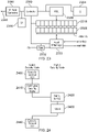
- Figure 1 schematically illustrates a data processing system 10 comprising a processor 20 coupled to a memory 30 storing data values 32 and program instructions 34.
- the processor 20 includes an instruction fetch unit 40 for fetching program instructions 34 from the memory 30 and supplying the fetch program instructions to decoder circuitry 50.
- Vector processing circuitry 52 comprises decoder circuitry 50 and instruction processing circuitry 60.
- the decoder circuitry 50 decodes the fetched program instructions and generates control signals to control the instruction processing circuitry 60 to perform vector processing operations upon vector registers stored within vector register circuitry 70 as specified by the decoded vector instructions.
- the processor 20 also comprises scalar processing circuitry 80 associated with scalar registers 90.
- Scalar processing involves applying a single vector processing instruction to data items of a data vector having a plurality of data items at respective positions in the data vector.
- Scalar processing operates on, effectively, single data items rather than on data vectors.
- Vector processing can be useful in instances where processing operations are carried out on many different instances of the data to be processed.
- a single instruction can be applied to multiple data items (of a data vector) at the same time. This can improve the efficiency and throughput of data processing compared to scalar processing.
- Embodiments of the present disclosure include an apparatus, for example of the type shown in Figure 1 , operable or configured to decode and execute such program instructions.
- Figure 1 therefore provides an example of vector processing circuitry to selectively apply vector processing operations defined by vector processing instructions to generate one or more data elements of a data vector comprising a plurality of data elements at respective data element positions of the data vector, according to the state of respective predicate flags associated with the positions of the data vector.
- the predicate flags are stored in a register file 72, forming one of the set of vector registers 70.
- a generator 55 is associated with the decoder circuitry 50 and the instruction processing circuitry 60.
- the generator 55 carries out a sampling process so as to generate instruction sample data 65 indicative of the operations of at least the instruction processing circuitry 60.
- sampling relates to the fact that the data 65 is not generated for every instruction executed by the instruction processing circuitry 60 (as might be the case in the generation of so-called trace data) but rather a sample of instructions is selected by the generator 55 and potentially detailed information acquired as the instruction sample data about the selected instructions.
- the ratio of sampled instructions to total instructions executed is a matter of a design choice, but typically the ratio might be of the order of one in a thousand to one in several hundreds of thousands of instructions which are sampled. It can be useful for the ratio to be such that the process of generating the instruction sample data for a particular executed instruction can be completed by the time that the next instruction is sampled, so that there is no need to handle an ongoing pipeline of sample data.
- the sampling can be regular, for example every nth instruction (where n is perhaps 10000), which can be referred to as so-called systematic sampling of the instructions.
- the generator 55 writes the instruction sample data to main memory, for example to a reserved or otherwise allocated region 36 of memory. In doing so, the generator 55 maintains a count (for example, using a counter 57) of the amount of data written to the region 36.
- a threshold level of occupancy such as 95% or even 100%
- the generator issues an interrupt 75 to the processor 20 to cause the processor to: (i) output the instruction sample data from the region 36 to an analysis processor 95 such as a general purpose computer running appropriate analysis software, and (ii) reset the counter 57.
- the instruction sample data can relate to many different aspects of the operation of the processor 20. In the present examples, it relates at least in part to the state of the predicate flags at execution of a sampled instruction. This feature will be discussed in more detail below.
- the generator 55 therefore provides an example of generator circuitry to generate instruction sample data indicative of processing activities of the vector processing circuitry for selected ones of the vector processing instructions, instruction sample data indicating at least the state of the predicate flags at execution of the selected vector processing instructions.
- the storage of instruction sample data associated with the state of the predicate flags can be useful in the performance monitoring, debugging and other analysis of vector processing circuitry. To achieve a useful gain in efficiency over scalar processing, it is appropriate for the vectorised or parallel nature of the processing to be utilised. If a significant number of predicate flags are set to inactive in respect of the sampled instructions, this can indicate that the system is not efficiently using the parallel vector processing available to it and/or is potentially wasting power by running a vectorised system that is not being appropriately utilised, and so this can potentially prompt further investigation or diagnosis, or potentially a reversion to using scalar processing for the processing task under consideration.
- the vector processing circuitry comprises: instruction decoder circuitry 50 to decode program instructions; and instruction processing circuitry 60 to execute instructions decoded by the instruction decoder circuitry in dependence upon the predicate flags.
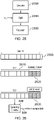
- Figure 2 schematically illustrates the handling of data as multiple data vectors.
- a set of data items 100 are intended to be processed in a processing order 110.
- the data items 100 are in fact handled as successive data vectors 120 so that in a vector processing operation, a single vector processing instruction is applied to all of the data items in the data vector (for example, 4 data items, 8 data items or whatever the prevailing vector length VL of the particular system is) simultaneously.
- each data vector 120 can retain a data item processing order 130, and from vector to vector there can be a vector processing order 140, so that if any reference is needed during processing to the original processing order 110, this can be achieved by considering the data vectors in the vector processing order 140 and considering data items within each data vector in the data item processing order 130.
- Figure 3 schematically illustrates the use of predicate flags to control vector processing operations.
- Predicate flags comprise flag information provided for each data item position within a data vector to indicate whether a processing operation should be carried out in respect of that data item position.
- the instruction processing circuitry 60 can access multiple sets of predicate flags, such that any particular vector processing operation can refer to one or more sets of predicate flags as parameters to that vector processing operation.
- An example input data vector 250 (Vector A) is to be the subject of a vector processing operation 260 such that, in the absence of any control by predicate flags, the vector processing operation 260 would be applied to each data item position.
- a set of predicate flags 270 one for each data item position or "lane", is also provided to control the vector processing operation.
- the data items 252 of the input vector are processed according to the vector processing operation 260 to generate data items 282 of an output data vector 280 (vector B). If the predicate flag 272 corresponding to a data item position in the output data vector 280 is set to "active" (for example, a value of 1). If the corresponding predicate flag for an output vector position is set to "inactive" (for example, a value of 0) then the vector processing operation 260 in respect of that output vector position is not carried out.
- the predicate flags control whether a vector processing operation for a particular output position or "lane" in relation to the output data vector 280 is carried out.
- predicate flags could be used to control whether data item positions in the input vector (or one or more input vectors) 250 are used.
- the predicate flags indicate whether processing is active or inactive at each data element position, a data element being generated by the vector processing operations at a data element position at which processing is active.
- predicate flags having an active state indicating that the vector processing instruction should be applied to those positions of a data vector corresponding to predicate flags in the active state.
- An inactive state indicates that the vector processing operation should not be so applied.
- a vector processing operation is not carried out in respect of a particular output vector position 282, because of an inactive predicate flag, then in some examples a fixed value such as 0 can be inserted into that output position. In other examples the previous contents, whatever they are, of that output position can be left unchanged.
- predicate flags in this manner therefore provides an example of applying a vector processing instruction to one or more data items of a data vector comprising a plurality of data items at respective positions in the data vector, according to the state of respective predicate flags associated with the positions.
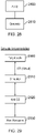
- Figure 4 is a schematic diagram illustrating some of the functionality of the generator 55.
- a selector 400 selects an instruction on which a sampling process should be performed so as to generate instruction sample data 410. In some examples to be discussed in more detail below, the selector 400 achieves this by counting decoded instructions from the decoder 50 and sampling, for example, every nth instruction where n is perhaps of the order of 1000 or 10000.
- the selector 400 instructs a sampler 420 to generate the instruction sample data 410 indicative of the execution of that instruction.
- the sampler 420 can be provided as inputs with the decoded instruction 430 itself (for example in order to detect an instruction type and optionally a word length associated with the instruction, a feature which will be discussed in connection with Figure 7 below), the predicate flags 440 applicable at the time of execution of the sampled instruction and optionally other data relating to the execution of the instruction such as values in processor registers or the like.
- the generator circuitry is responsive to decoding of a selected instruction by the instruction decoder circuitry 50 to initiate generation of the instruction sample data, and is responsive to the instruction processing circuitry to generate the instruction sample data indicating the state of the predicate flags at the time of execution of the selected instruction.
- the sampler 420 prepares instruction sample data 410 associated with the sampled instruction.
- Figure 5 schematically illustrates an example of the operation of the selector 400.
- a counter 500 counts successive instructions received from the decoder 50.
- the count may be, for example, an upwards count (for example from zero) or a downwards count (for example to zero). More generally, the count is from a start count value to a final count value.
- a comparator 510 compares the current count value with a threshold value 520 (representative of the final count value) and when the count value reaches the threshold value, an associated instruction at that count position, such as an instruction 530, is selected for sampling.
- the threshold 520 can be derived from a base value 540 added by an adder or other combiner 550 with a modifier value 560 such as a random or pseudo-random value, for example applicable to a particular number of least significant bits (LSBs) of the base value.
- a modifier value 560 such as a random or pseudo-random value, for example applicable to a particular number of least significant bits (LSBs) of the base value.
- the randomised or pseudo-randomised threshold can be applied as the start count value or the final count value depending on which way the counting is progressing.
- instruction selection circuitry (embodied by the selector 400) to select the selected (sampled) ones of the instructions comprises counter circuitry is configured to count instructions between a start count value and a final count value, and to select, as a selected instruction, an instruction for which the counter reaches the final count value.
- the instruction selection circuitry can be configured to combine one or both of the start count value and the final count value with a modifier value, such as a random or pseudorandom number.
- Figure 6 schematically illustrates one aspect of the operation of the sampler 420, involving a counter operation 600 which counts the number of predicate flags indicative of active processing in the respective vector lane.
- the output of the counter 610 can be, for example, a count such as 8, 12, 14... to indicate a number of the predicate flags indicating that processing is active and/or so-called event data such as flag indicating either that no predicate flags were set or a flag indicating that all available predicate flags were set, or in other words to selectively indicate at least one of: all predicate flags indicate that processing is active; at least some predicate flags indicate that processing is inactive; and all predicate flags indicate that processing is inactive.
- event data in this way allows a potentially lower data quantity to be used for the instruction sample data while still providing potentially useful information about the state of the predicate flags.
- Figure 7 schematically illustrates another potential aspect of the operation of the sampler 420, in that, for an instruction opcode 700 which specifies a data element or word length 710 as part of the opcode, a detector 720 generates, as at least a part of the instruction sample data 410, data 730 indicative of the word length applicable to the current sampled instruction.
- At least some of the vector processing instructions are configured to define a data element size from a set of candidate data element sizes, and in which the instruction sample data for a given vector processing instruction indicates a data element size applicable to execution of the given vector processing instruction.
- the data element size applicable to execution of that instruction is defined by at least a part of that vector processing instruction.
- Figure 8 schematically illustrates a feature of the predicate flags which may apply in the context of a system having a variable word length.
- a predicate flag 800 is applicable to an instance of the shortest available word length.
- the ratio of predicate flags to vector processing lanes, for a particular vector length may be greater than 1:1.
- the same vector length will provide a smaller number of vector processing lanes, so that, for example, a pair 810 of predicate flags may be applicable to an individual vector processing lane at a longer word length.
- a group of four or more predicate flags may be applicable to a single lane.
- a convention is sometimes provided by which, of a group of predicate flags associated with a data element such as the group 810, a subset of that group, such as the predicate flag 800 (for example, the predicate flag at the least significant position applicable to that lane), is used to indicate whether processing is active or inactive at that data element position.
- the other predicate flag 820 of the group 810 is redundant and can have an unspecified value.
- each data element is associated with a group of predicate flags associated with data element, in which a subset of the group of predicate flags indicates active or inactive processing at that data element position.
- the subset of predicate flags may comprise one predicate flag 800 of each group 810 of predicate flags.
- the present disclosure recognises that in a sampled system in which, for example, the number of predicate flags is counted as discussed above, having predicate flags such as the predicate flag 820 with an undefined value and a redundant function could potentially lead to a generation of misleading instruction sample data.
- the generator 55 optionally comprises so called modifying logic 830 which acts, for a given group of predicate flags such as the group 810, to set predicate flags (such as the redundant flag 820) other than the subset of predicate flags 800 to the same state as the state of the subset of predicate flags. Then, sampling takes place for example counting, by sampling circuitry 840 using the techniques described above to generate instruction sample data 850.
- modifying logic 830 acts, for a given group of predicate flags such as the group 810, to set predicate flags (such as the redundant flag 820) other than the subset of predicate flags 800 to the same state as the state of the subset of predicate flags. Then, sampling takes place for example counting, by sampling circuitry 840 using the techniques described above to generate instruction sample data 850.
- the modifying logic 830 sets the predicate flag 820 to "active".
- modifying logic 830 need not (and in these examples, does not) modify the actual predicate flags referred to by the processor 20, but just the flags which are processed by the sampling circuitry 840.
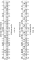
- Figures 9 to 22 which in each case represent a 256-bit vector (by way of example) arranged from a most significant bit at the left hand side of the drawing to a least significant bit at the right hand side of the drawing.
- An upper row labelled “V” represents the vectors in use and a lower row labelled “P” represents the predicate flags.
- a notation of "1” represents “active” and "0” represents “inactive”.
- a value of "X” represents an undefined or indeterminate value in a redundant predicate flag position.
- the predicate flags at positions 0, 8, 16, 24 represent the subset corresponding to the predicate flag 800 of Figure 8 .
- 32 predicate flags are provided for the 256 bit vector because the minimum word length in this example is 8 bits.
- the predicate flags at positions 1... 7, 9... 15, 17...23 and 25...31 are undefined because they are not relevant to a determination by the instruction processing circuitry 60 as to whether the vector lane is active or inactive.
- the predicate flags at positions 0, 4, 8, 12, 16, 20, 24, 28 represent the subset which are relevant to the determination by the instruction processing circuitry 60 as to whether that vector processing lane is active or inactive, and the remaining predicate flags are undefined.
- Figure 11 shows an arrangement similar to that of Figure 10 , except that all of the vector lanes are inactive as shown by the predicate flags "0" at the subset of positions.
- Figure 13 returns to the 4x64-bit example of Figure 9 , but using the same set of predicate flags as that of Figure 12 , although in this case because only the positions 0, 8, 16, 24 are in the subset indicative of an active or inactive status, all of the 64-bit elements are considered active.
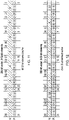
- a further row of values labelled as "S" represents the sampled values 835 sampled by the sampling circuitry 840 as modified by the modifying logic 830.
- the modifying logic does not need to modify the actual predicate values referred to by the processor 20, but rather modifies the way that the values that are counted.
- Figures 14 to 18 show the same vector and predicate values as Figures 9 to 13 .
- Figures 19 to 23 show the same predicate values.
- the modifying logic 830 has set predicate flags other than the subset (0, 8, 16, 24) of predicate flags in a 64-bit element system to the same state of that of the subset of predicate flags, for the purposes of counting. So, for each element position or lane, the state of the predicate flag indicative of an active or inactive status for that lane is replicated across other predicate flags associated with that lane.
- a count value applicable to this arrangement is 32 which indicates that all predicate values were set.
- the 8x32-bit lanes are all inactive and in the data 835 output by the modifying logic 830, predicate flags other than the subset (0, 4, 8, 12, 16, 20, 24, 28) are set to the same status the respective subset of predicate flags leading to a count of zero.
- Figure 17 is an example of 8 x 32-bit elements in which even lanes are active and odd lanes are inactive. By applying the technique described above, the count value is 16 which indicates correctly that half of the lanes are active and half inactive.
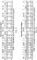
- Figure 18 is an example of 4 x 64-bit elements all of which are active, with the process of the modifying logic 830 leading to a count of 32 active predicate flags.
- Figure 19 shows an example of 32 x 8-bit elements such that each predicate flag position represents an individual processing lane. In the example shown, the count is 15.
- Figure 20 shows an example of 16 x 16-bit elements some of which that are active and some inactive, but by applying the processing of the modifying logic 830, a count of 14 is obtained indicating correctly that a proportion of 14/32 of the elements are active.
- Figure 21 relates to an 8 x 32-bit arrangement, once again in which the processing of the modifying logic 830 leads to a count of 16, correctly indicating that 50% of the lanes are active.
- Figure 22 is a 4 x 64-bit element example, in which the processing of the modifying logic 830 again leads to a count of 32, correctly indicating that all lanes are active.
- Figure 23 schematically illustrates control circuitry and part of the vector processor.
- Vector processing is applied by carrying out the same processing operation, generally in parallel, in respect of a set or vector of data items.
- This arrangement can rely upon various calculation components and register storage for each of the processing lanes (one processing lane corresponding to the processing applied to one data item in a data vector).
- a set of registers 2300 and a set of calculation and control elements 2310 provide a simplified representation of the processing arrangements used by the vector processor. There are one register 2300 and one processing element 2310 for each processing lane (though it will be appreciated that many more components may be involved in a real implementation of a processing lane).
- the total number of processing lanes shown in Figure 23 corresponds to the maximum possible data vector length ("Max VL") of the system. This is a physical upper limit on the data vector width and represents the number of processing lanes available to the vector processor if all of them are enabled by control circuitry 2360 (that is to say, if a current subset of disabled lanes is zero). However, in the present embodiments, under the control of the control circuitry 2360 a smaller data vector width can be selectively used instead of the maximum data vector width Max VL.
- Max VL could be much larger than that shown schematically in Figure 23 .
- Max VL could be 256 bit, 512 bit, 1024 bit or another value.
- "256 bit” represents up to 32 8-bit elements, or up to 16 16-bit elements, or up to 4 64-bit elements.
- the example value of Max VL in Figure 23 is simply for the purposes of explanation.
- the control circuitry 2360 is configured to disable operation of a subset of the processing lanes so that the disabled subset of processing lanes are unavailable for use by the vector processing circuitry, in response to a current value of VL stored in a register 2390, and maintained by the control circuitry 2360 in response to execution of instructions to change VL to be discussed below.
- the use of the register 2390 therefore provides an example of a current vector length being defined by a processor register having a register state which is responsive to execution of a vector length defining instruction.
- This selective disabling can be achieved in various ways.
- control circuitry 2360 controls the operation of a power supply unit (PSU) 2320 which supplies power to at least parts of (or all of) each of the respective processing lanes, so as to selectively remove power from the subset of (disabled) processing lanes, for example by disabling a power supply to the subset of processing lanes.
- PSU power supply unit
- control circuitry 2360 supplies a control signal to the subset of processing lanes so as to disable operation of the respective processing element 2310.
- the processing elements can include, for example, arithmetic logic units, multipliers and the like, which can be selectively disabled by disconnection form the remaining circuitry, power supply gating or clock gating (see below).
- read/write logic 2330 which controls the reading from and writing to the register elements 2300, act under the control of the control circuitry 2360 so as to inhibit reading from or writing to register elements 2300 corresponding to the subset of (disabled) processing lanes.
- each processing lane comprises one or more data registers such as the register elements 2300
- the vector processing circuitry is configured to load data from a memory (not shown in Figure 23 , but shown as the memory 30 in Figure 1 ) into the data registers and to write data from the registers to the memory; and the control circuitry 2360 is configured to inhibit the vector processing circuitry from writing data to the memory from data registers corresponding to the subset of processing lanes.
- the registers corresponding to currently disabled processing lanes can be entirely disabled or powered down, or their contents can be retained (either by providing power to them, or by using a non-volatile memory element for the registers 2300), though in such a way that access to those registers corresponding to currently disabled processing lanes is prevented or inhibited.
- the control circuitry 2360 can apply a so-called clock-gating process.
- An example is shown schematically in Figure 23 in respect of the read/write logic 2330, but the same arrangement can be applied to other aspects of the processing lanes such as the registers 2300 and/or the processing elements 2310.
- a clock signal CK is processed by a clock gate 2332 before being supplied to the read/write logic (or to parts of the read/write logic applicable to disabled processing lanes).
- the clock gate 2332 passes or blocks the clock signal CK. So, as at least a part of disabling one or more processing lanes, the clock signal CK can be blocked from one or more components relating to those processing lanes.
- Disabling the subset of processing lanes can also (or instead) involve disabling (for example, by clock gating or power gating) communication circuitry such as bus drivers relating to the disabled lanes.
- the sets of processing elements and registers may include so-called permute logic arranged to conduct cross-lane operations (where the contents of a register can depend upon operations carried out with respect to the contents of one or more other registers).
- the permute logic operates under the control of the control circuitry 2360 so as to be inhibited from carrying out operations which do either or both of (a) deriving the contents of a currently active lane from those of one or more currently disabled lanes, and (b) deriving the contents of a currently disabled lane.
- Predicate flags provide conditional execution relating to respective processing lanes of a vector processor. In such situations the lanes remain available for use by the vector processor. In the present arrangements, by contrast, the subset of processing lanes is disabled so as to be unavailable for use by the vector processor, the vector processor operates as though it simply has a smaller number of processing lanes than the number corresponding to the maximum data vector length. Disabled lanes in the context of the present application are not written back to memory.
- Predicated lanes may be preserved as part of register write-backs.
- a merging vector load may only load a subset of element while preserving the remaining values originally held by the designation register.
- renaming may require the move of those remaining values from the destination register prior to renaming to the newly renamed register. Examples of the present system may not make any guarantees about the content of disabled lanes.
- control circuitry 2360 is configured to selectively disable operation of a portion of the data structure(s) in an instruction queue 2364 in dependence upon the data vector length set by the control circuitry, for example by controlling power supply to those data structures and/or by clock-gating those data structures as discussed above.
- the instruction sample data for a given vector processing instruction indicates a vector length applicable to execution of the given vector processing instruction.
- the generator comprising a VL data generator 2380 configured to generate instruction sample data 2385 indicative of the current VL applicable to execution of a sample instruction, as stored in the register 2390.
- Figure 24 is a schematic flow chart showing an example of the setting of a vector length in the register 2390 by the control circuitry 2360.
- the vector length for use by a lower security mode can only be set by program code operating in a higher security mode.
- any instruction could be used to change VL.
- the processor 20 is configured to perform processing activities in two or more security modes.
- the security modes can be arranged so as to inhibit a processing activity performed in one of the security modes from accessing at least some information associated with a processing activity performed in another of the security modes.
- two or more security modes including a higher security level mode and a lower security level mode may be provided, such that operations of the processor 20 in a lower security level mode cannot access (or at least is inhibited from accessing) at least some information (such as register contents, or parts of the address space) associated with operations of the processing element in a higher security level mode.
- two or more mutually exclusive security modes could be provided, so that when the processor 20 is operating in one of the two or more complementary security modes, it cannot access at least some information associated with operations in another of the two or more complementary security modes.
- One use of different security modes of a processor is in the context of virtualisation, in which multiple operating systems co-exist on a single processor as so-called virtual machines, each under the control or oversight of a so-called hypervisor.
- Various steps can be taken to avoid inappropriate interference between the different virtual machines. For example, applications can run at a lowest security level; operating systems can run at a next higher security level, and the hypervisor can run at a still higher security level. In this way, protection can be built into the system to avoid (for example) an application running under one of the operating systems corrupting information used by an application running under another of the operating systems.
- a temporary change in security mode can be implemented as a branch from program instructions running in one security mode to a function or subroutine under a different security mode.
- the processor 20 In order to allow registers associated with the processor to be used in the second (new) security mode without necessarily disclosing or allowing corruption of the content of those registers as used by the first (original) security mode, it can be appropriate for the processor 20 to store those registers in memory storage such as a processor stack. This also allows the processing activity in the first security mode to resume with the same register parameters that applied when the branch to the function or subroutine took place.
- program code is executed under the lower security mode according to a data vector length VL1.
- the program code in the lower security mode makes a call to the higher security mode.
- Control is transferred to the higher security mode and, at a step 2420, program code running under the higher security mode sets the vector length applicable to the lower security mode to a new vector length VL2, by executing vector length changing instruction as an example of at least some of the vector processing instructions being vector length defining instructions configured to define a vector length of the data vector. This changes the prevailing VL value in the register 2390.
- the lower security mode executes program code at the vector length VL2.
- the process of setting a vector length VL by the control circuitry 2360 may allow for any VL value between 1 (or 2, in order for the term "vector" to apply in a useful way) up to VL Max.
- the selectable values of VL are limited to a subset of all such available values.
- both VL Max and a selectable value of VL may be restricted to be multiples of a particular value such as multiples of 128.
- Max VL is 1024
- VL can be set by the control circuitry 62 to be any one of 128, 256, 384, 512, 640, 768, 896 or 1024 bits (see the discussion above).
- At least some components used by the vector processor can be arranged in banks of (say) 128-bit wide units, so that clock gating, power gating or other techniques can be applied on a bank-by-bank basis rather than requiring individual attention to each such element.
- the Set VL instruction can implement a change to an absolute value of vector length, for example "Set VL to 64".
- the Set VL instruction is defined and executed so as to set the vector length to a particular proportion of Max VL, whatever Max VL is on that particular data processing apparatus.
- the instruction could be of the form "Set VL to Max VL / 4".
- the vector lengths VL1, VL2 in the present discussion should therefore be interpreted either as an absolute vector length or as a relative vector length expressed with reference to the Max VL of the particular executing apparatus.
- Max VL values which are powers of two, and Set VL instructions which vary VL by powers of two relative to Max VL, are useful in this context. Therefore, different versions or "flavours" of Set VL can be considered.
- Set VL can act according to an immediate or register-dependent operand defining a multiple of a fixed size (such as 128-bit). This can be capped at Max VL.
- Set VL can act according to an immediate or register-dependent operand describing a fraction of whatever the prevailing VL Max value is (such as 1, 1/2, 1/4, 1/8, ).
- VL While there is not necessarily a structural limitation on how often VL can be changed, it can be appropriate for the system (under program control, for example) not to make changes more often than, say every 100 or 1000 instructions. This can help to avoid or reduce inefficiencies resulting from operations and administration (for example, changing security level, or stalling decoding as discussed below) occurring at a change of VL.
- Figure 25 schematically illustrates the operation of decoder circuitry such as the decoder circuitry 50 of Figure 1 .
- the flow chart of Figure 25 is simplified for the purposes of illustrating technical points relevant to the present discussion. It will be appreciated that further operations may be performed as part of the operation of the decoding circuitry 50.
- the decoder circuitry 50 is (optionally) operable to decode vector processing instructions into sets of operations, the number of sets being equal to the data vector length, which in the present embodiments is set by the control circuitry 2360. This can occur, for example, for multiple stage instructions such as scatter, gather and the like. Other operations are carried out as single vector processing instructions.
- a step 2500 involves decoding a vector processing instruction.
- the decoded instruction is split or "cracked” into sets of operations applied to data items 100 of successive data vectors 120 as discussed with reference to Figure 2 .
- the operation at the step 2510 is responsive to the current vector length (VL) established by the control circuitry 2360 and stored in the register 2390.
- the sets of operations are dispatched for execution by the vector processor.
- the operations of the steps 2500, 2510 by the decoder circuitry 50 provide an example of an instruction decoder to decode vector processing instructions into sets of operations, the number of sets being equal to the data vector length set by the control circuitry.
- the vector length applicable to a particular instruction can result from the active setting of VL, for example by a VL-setting instruction as discussed above, and/or the contents of a VL register as discussed above, and/or as a result of a cracking operation of the type discussed with reference to Figure 25 .
- the instruction sample data for a given vector processing instruction can indicate a vector length applicable to execution of the given vector processing instruction.
- the instruction sample data for a given vector processing instruction indicates (as well as a vector length applicable to the given instruction) a data element size applicable to the given instruction and data indicating the state of each of the predicate flags applicable to execution of the given instruction.
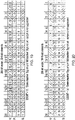
- Figure 26 schematically illustrates an example of maximum vector length max VL 2600, in which the processing described above imposes a reduced vector length VL1 2610 such that a subset 2620 of processing lanes is at least temporarily disabled .
- the modifying logic 830 is configured to set the predicate flags 2630 corresponding to the disabled subset 2620 to a predetermined state such as "inactive", so that the sampling circuitry 840 can generate the instruction sampled data 850 based on a count of predicate flags including an inactive state for the flags 2630 corresponding to the disabled subset 2620.
- Figure 27 illustrates a system having a maximum vector length of 256 bits, but which is set to a current vector length of 128 bits.
- the modifying logic 830 generates the data for sampling ("S") in which vector positions 16...31 associated with the disabled lanes 128...255 are set to "inactive". This means that the count of active positions is based only on the currently enabled lanes and gives a correct value of 8.
- This arrangement provides an example in which the generator circuitry is configured, for a given group of predicate flags, to generate instruction sample data which indicates that predicate flags relating to data elements not included in a vector of the current vector length are set to a predetermined state.
- Figure 28 is a schematic flowchart illustrating a vector processing method comprising:
- Figure 29 illustrates a simulator implementation that may be used. Whilst the earlier described embodiments implement the present invention in terms of apparatus and methods for operating specific processing hardware supporting the techniques concerned, it is also possible to provide an instruction execution environment in accordance with the embodiments described herein which is implemented through the use of a computer program. Such computer programs are often referred to as simulators, insofar as they provide a software based implementation of a hardware architecture. Varieties of simulator computer programs include emulators, virtual machines, models, and binary translators, including dynamic binary translators. Typically, a simulator implementation may run on a host processor 2930, optionally running a host operating system 2920, supporting the simulator program 2910.
- the hardware there may be multiple layers of simulation between the hardware and the provided instruction execution environment, and/or multiple distinct instruction execution environments provided on the same host processor.
- powerful processors have been required to provide simulator implementations which execute at a reasonable speed, but such an approach may be justified in certain circumstances, such as when there is a desire to run code native to another processor for compatibility or re-use reasons.
- the simulator implementation may provide an instruction execution environment with additional functionality which is not supported by the host processor hardware, or provide an instruction execution environment typically associated with a different hardware architecture.
- the simulator program 2910 may be stored on a computer-readable storage medium (which may be a non-transitory medium), and provides a program interface (instruction execution environment) to the target code 2900 (which may include applications, operating systems and a hypervisor) which is the same as the application program interface of the hardware architecture being modelled by the simulator program 2910.
- the program instructions of the target code 2900 including instructions to generate instruction sample data indicative of processing activities of the vector processing circuitry for selected ones of the vector processing instructions, instruction sample data indicating at least the state of the predicate flags at execution of the selected vector processing instructions as described above, may be executed from within the instruction execution environment using the simulator program 2910, so that a host computer 2930 which does not actually have the hardware features of the apparatus discussed above can emulate these features.
- the simulator arrangement of Figure 29 when configured to simulate the apparatus described above, provides an example of a computer program for controlling a host data processing apparatus to provide an vector instruction execution environment comprising: vector processing program logic to selectively apply vector processing operations defined by vector processing instructions to generate one or more data elements of a data vector comprising a plurality of data elements at respective data element positions of the data vector, according to the state of respective predicate flags associated with the positions of the data vector; and generator program logic to generate instruction sample data indicative of processing activities of the vector processing circuitry for selected ones of the vector processing instructions, instruction sample data indicating at least the state of the predicate flags at execution of the selected vector processing instructions.
- the words “configured to" are used to mean that an element of an apparatus has a configuration able to carry out the defined operation.
- a “configuration” means an arrangement or manner of interconnection of hardware or software.
- the apparatus may have dedicated hardware which provides the defined operation, or a processor or other processing device may be programmed to perform the function.
- Configured to does not imply that the apparatus element needs to be changed in any way in order to provide the defined operation.
Landscapes
- Engineering & Computer Science (AREA)
- Theoretical Computer Science (AREA)
- Software Systems (AREA)
- Physics & Mathematics (AREA)
- General Engineering & Computer Science (AREA)
- General Physics & Mathematics (AREA)
- Mathematical Physics (AREA)
- Computer Hardware Design (AREA)
- Quality & Reliability (AREA)
- Computing Systems (AREA)
- Executing Machine-Instructions (AREA)
- Advance Control (AREA)
- Complex Calculations (AREA)
Claims (15)
- Datenverarbeitungsvorrichtung, die aufweist:eine Vektorverarbeitungsschaltungsanordnung (52) zum selektiven Anwenden von Vektorverarbeitungsoperationen, die durch Vektorverarbeitungsanweisungen definiert sind, um ein oder mehrere Datenelemente eines Datenvektors, der eine Mehrzahl von Datenelementen umfasst, an jeweiligen Datenelementpositionen des Datenvektors zu erzeugen, gemäß dem Zustand jeweiliger Prädikat-Flags, die den Positionen des Datenvektors zugeordnet sind; undeine Erzeugerschaltungsanordnung zum Erzeugen von Anweisungsabtastdaten, die Verarbeitungsaktivitäten der Vektorverarbeitungsschaltungsanordnung (52) für ausgewählte der Vektorverarbeitungsanweisungen angeben, wobei Anweisungsabtastdaten mindestens den Zustand der Prädikat-Flags bei der Ausführung der ausgewählten Vektorverarbeitungsanweisungen angeben; undeine Anweisungsauswahlschaltungsanordnung zum Auswählen der ausgewählten der Vektorverarbeitungsanweisungen, wobei die Anweisungsauswahlschaltungsanordnung eine Zählerschaltungsanordnung (500) umfasst, die dazu ausgelegt ist, Anweisungen zwischen einem Startzählwert und einem Endzählwert zu zählen und eine Anweisung, für die der Zähler den Endzählwert erreicht, als eine ausgewählte Anweisung auszuwählen.
- Vorrichtung nach Anspruch 1, wobei die Prädikat-Flags anzeigen, ob die Verarbeitung an jeder Datenelementposition aktiv oder inaktiv ist, wobei ein Datenelement durch die Vektorverarbeitungsoperationen an einer Datenelementposition erzeugt wird, an der die Verarbeitung aktiv ist; oderwobei mindestens einige der Vektorverarbeitungsanweisungen vektorlängendefinierende Anweisungen sind, die dazu ausgelegt sind, eine Vektorlänge des Datenvektors zu definieren, und wobei eine aktuelle Vektorlänge durch ein Prozessorregister definiert ist, das einen Registerzustand aufweist, der auf die Ausführung einer vektorlängendefinierenden Anweisung reagiert; oderwobei die Anweisungsauswahlschaltungsanordnung dazu ausgelegt ist, den Startzählwert oder den Endzählwert oder beide mit einem Modifikatorwert zu kombinieren.
- Vorrichtung nach Anspruch 1, wobei die Anweisungsabtastdaten eine Anzahl der Prädikat-Flags angeben, die anzeigen, dass die Verarbeitung aktiv ist.
- Vorrichtung nach Anspruch 3, wobei Anweisungsabtastdaten Ereignisdaten umfassen, um mindestens einen der folgenden Zustände selektiv anzugeben:alle Prädikat-Flags zeigen an, dass die Verarbeitung aktiv ist;mindestens einige Prädikat-Flags zeigen an, dass die Verarbeitung inaktiv ist; undalle Prädikat-Flags zeigen an, dass die Verarbeitung inaktiv ist.
- Vorrichtung nach Anspruch 1, wobei mindestens einige der Vektorverarbeitungsanweisungen dazu ausgelegt sind, eine Datenelementgröße aus einem Satz von Kandidatendatenelementgrößen zu definieren, und wobei die Anweisungsabtastdaten für eine gegebene Vektorverarbeitungsanweisung eine Datenelementgröße angeben, die für die Ausführung der gegebenen Vektorverarbeitungsanweisung geeignet ist.
- Vorrichtung nach Anspruch 5, wobei für mindestens einige der Vektorverarbeitungsanweisungen die Datenelementgröße, die für die Ausführung dieser Anweisung geeignet ist, durch mindestens einen Teil dieser Vektorverarbeitungsanweisung definiert ist.
- Vorrichtung nach Anspruch 5, wobei für mindestens einige Datenelementgrößen des Satzes von Kandidatendatenelementgrößen jedes Datenelement einer Gruppe von Prädikat-Flags, die einem Datenelement zugeordnet sind, zugeordnet ist, wobei ein Teilsatz der Gruppe von Prädikat-Flags eine aktive oder inaktive Verarbeitung an dieser Datenelementposition anzeigt.
- Vorrichtung nach Anspruch 7, wobei der Teilsatz von Prädikat-Flags ein Prädikat-Flag aus jeder Gruppe von Prädikat-Flags aufweist; oder
wobei die Erzeugerschaltungsanordnung für eine gegebene Gruppe von Prädikat-Flags dazu ausgelegt ist, Anweisungsabtastdaten zu erzeugen, die angeben, dass andere Prädikat-Flags als der Teilsatz von Prädikat-Flags den gleichen Zustand aufweisen wie der Zustand des Teilsatzes von Prädikat-Flags. - Vorrichtung nach Anspruch 1, wobei die Anweisungsabtastdaten für eine gegebene Vektorverarbeitungsanweisung eine Vektorlänge angeben, die für die Ausführung der gegebenen Vektorverarbeitungsanweisung geeignet ist.
- Vorrichtung nach Anspruch 9, wobei die Anweisungsabtastdaten für die gegebene Vektorverarbeitungsanweisung eine Datenelementgröße, die für die gegebene Anweisung geeignet ist, und Daten, die den Zustand jedes der Prädikat-Flags angeben, die für die Ausführung der gegebenen Anweisung geeignet sind, angeben.
- Vorrichtung nach Anspruch 10, wobei die Erzeugerschaltungsanordnung für eine gegebene Gruppe von Prädikat-Flags dazu ausgelegt ist, Anweisungsabtastdaten zu erzeugen, die angeben, dass Prädikat-Flags, die sich auf Datenelemente beziehen, die nicht in einem Vektor der aktuellen Vektorlänge enthalten sind, auf einen vorbestimmten Zustand gesetzt sind.
- Vorrichtung nach Anspruch 1, wobei die Vektorverarbeitungsschaltungsanordnung (52) aufweist:eine Anweisungsdecoderschaltungsanordnung zum Decodieren von Programmanweisungen; undeine Anweisungsverarbeitungsschaltungsanordnung zum Ausführen von Anweisungen, die von der Anweisungsdecoderschaltungsanordnung in Abhängigkeit von den Prädikat-Flags decodiert werden.
- Vorrichtung nach Anspruch 12, wobei die Erzeugerschaltungsanordnung auf das Decodieren einer ausgewählten Anweisung durch die Anweisungsdecoderschaltungsanordnung reagiert, um die Erzeugung der Anweisungsabtastdaten einzuleiten, und auf die Anweisungsverarbeitungsschaltungsanordnung reagiert, um die Anweisungsabtastdaten zu erzeugen, die den Zustand der Prädikat-Flags zu der Zeit der Ausführung der ausgewählten Anweisung angeben.
- Vektorverarbeitungsverfahren, das umfasst:selektives Anwenden (2800) von Vektorverarbeitungsoperationen, die durch Vektorverarbeitungsanweisungen definiert sind, um ein oder mehrere Datenelemente eines Datenvektors, der eine Mehrzahl von Datenelementen umfasst, an jeweiligen Datenelementpositionen des Datenvektors zu erzeugen, gemäß dem Zustand jeweiliger Prädikat-Flags, die den Positionen des Datenvektors zugeordnet sind; undErzeugen (2810) von Anweisungsabtastdaten, die Vektorverarbeitungsaktivitäten für ausgewählte der Vektorverarbeitungsanweisungen angeben, wobei Anweisungsabtastdaten mindestens den Zustand der Prädikat-Flags bei der Ausführung der ausgewählten Vektorverarbeitungsanweisungen angeben; undAuswählen der ausgewählten der Vektorverarbeitungsanweisungen, wobei der Schritt des Auswählens das Zählen von Anweisungen zwischen einem Startzählwert und einem Endzählwert und das Auswählen einer Anweisung, für die der Zählerstand den Endzählwert erreicht, als eine ausgewählte Anweisung umfasst.
- Computerprogramm zum Steuern einer Host-Datenverarbeitungsvorrichtung, um eine Vektoranweisungsausführungsumgebung bereitzustellen, aufweisend:Vektorverarbeitungsprogrammlogik zum selektiven Anwenden von Vektorverarbeitungsoperationen, die durch Vektorverarbeitungsanweisungen definiert sind, um ein oder mehrere Datenelemente eines Datenvektors, der eine Mehrzahl von Datenelementen umfasst, an jeweiligen Datenelementpositionen des Datenvektors zu erzeugen, gemäß dem Zustand jeweiliger Prädikat-Flags, die den Positionen des Datenvektors zugeordnet sind; undErzeugerprogrammlogik zum Erzeugen von Anweisungsabtastdaten, die Verarbeitungsaktivitäten der Vektorverarbeitungsschaltungsanordnung (52) für ausgewählte der Vektorverarbeitungsanweisungen angeben, wobei Anweisungsabtastdaten mindestens den Zustand der Prädikat-Flags bei der Ausführung der ausgewählten Vektorverarbeitungsanweisungen angeben; undAnweisungsauswahllogik zum Auswählen der ausgewählten der Vektorverarbeitungsanweisungen, wobei die Anweisungsauswahllogik Zählerlogik umfasst, die dazu ausgelegt ist, Anweisungen zwischen einem Startzählwert und einem Endzählwert zu zählen und eine Anweisung, für die der Zähler den Endzählwert erreicht, als eine ausgewählte Anweisung auszuwählen.
Applications Claiming Priority (2)
| Application Number | Priority Date | Filing Date | Title |
|---|---|---|---|
| GB1803250.8A GB2571527B (en) | 2018-02-28 | 2018-02-28 | Data processing |
| PCT/GB2019/050408 WO2019166772A1 (en) | 2018-02-28 | 2019-02-15 | Data processing |
Publications (2)
| Publication Number | Publication Date |
|---|---|
| EP3759592A1 EP3759592A1 (de) | 2021-01-06 |
| EP3759592B1 true EP3759592B1 (de) | 2022-04-13 |
Family
ID=61903155
Family Applications (1)
| Application Number | Title | Priority Date | Filing Date |
|---|---|---|---|
| EP19707083.2A Active EP3759592B1 (de) | 2018-02-28 | 2019-02-15 | Datenverarbeitung |
Country Status (7)
| Country | Link |
|---|---|
| US (1) | US11354126B2 (de) |
| EP (1) | EP3759592B1 (de) |
| JP (1) | JP7377208B2 (de) |
| KR (1) | KR102773317B1 (de) |
| CN (1) | CN111742296B (de) |
| GB (1) | GB2571527B (de) |
| WO (1) | WO2019166772A1 (de) |
Families Citing this family (3)
| Publication number | Priority date | Publication date | Assignee | Title |
|---|---|---|---|---|
| CN115644738A (zh) | 2021-02-10 | 2023-01-31 | 北京石头创新科技有限公司 | 清洁机器人脱困方法及装置、介质及电子设备 |
| GB2630043B (en) * | 2023-05-15 | 2025-08-06 | Advanced Risc Mach Ltd | Apparatus, method and computer program for monitoring performance of software |
| CN117093268B (zh) * | 2023-10-19 | 2024-01-30 | 超睿科技(长沙)有限公司 | 一种向量处理方法、系统、设备及存储介质 |
Family Cites Families (11)
| Publication number | Priority date | Publication date | Assignee | Title |
|---|---|---|---|---|
| US7017032B2 (en) * | 2001-06-11 | 2006-03-21 | Broadcom Corporation | Setting execution conditions |
| US20040064685A1 (en) * | 2002-09-27 | 2004-04-01 | Hung Nguyen | System and method for real-time tracing and profiling of a superscalar processor implementing conditional execution |
| US9116686B2 (en) * | 2012-04-02 | 2015-08-25 | Apple Inc. | Selective suppression of branch prediction in vector partitioning loops until dependency vector is available for predicate generating instruction |
| US9495169B2 (en) * | 2012-04-18 | 2016-11-15 | Freescale Semiconductor, Inc. | Predicate trace compression |
| WO2014147446A1 (en) | 2013-03-21 | 2014-09-25 | Freescale Semiconductor, Inc. | Data processing device, method of reporting predicate values, and data carrier |
| US9367309B2 (en) * | 2013-09-24 | 2016-06-14 | Apple Inc. | Predicate attribute tracker |
| US9323525B2 (en) * | 2014-02-26 | 2016-04-26 | Intel Corporation | Monitoring vector lane duty cycle for dynamic optimization |
| US9348595B1 (en) * | 2014-12-22 | 2016-05-24 | Centipede Semi Ltd. | Run-time code parallelization with continuous monitoring of repetitive instruction sequences |
| US9996347B2 (en) * | 2014-12-24 | 2018-06-12 | Intel Corporation | Hardware apparatuses and methods relating to elemental register accesses |
| GB2540941B (en) | 2015-07-31 | 2017-11-15 | Advanced Risc Mach Ltd | Data processing |
| EP3125108A1 (de) | 2015-07-31 | 2017-02-01 | ARM Limited | Datenverarbeitung |
-
2018
- 2018-02-28 GB GB1803250.8A patent/GB2571527B/en active Active
-
2019
- 2019-02-15 JP JP2020544207A patent/JP7377208B2/ja active Active
- 2019-02-15 KR KR1020207026708A patent/KR102773317B1/ko active Active
- 2019-02-15 EP EP19707083.2A patent/EP3759592B1/de active Active
- 2019-02-15 CN CN201980014746.9A patent/CN111742296B/zh active Active
- 2019-02-15 WO PCT/GB2019/050408 patent/WO2019166772A1/en not_active Ceased
- 2019-02-15 US US16/975,486 patent/US11354126B2/en active Active
Also Published As
| Publication number | Publication date |
|---|---|
| JP7377208B2 (ja) | 2023-11-09 |
| KR20200124251A (ko) | 2020-11-02 |
| US20210034362A1 (en) | 2021-02-04 |
| CN111742296B (zh) | 2024-08-16 |
| GB2571527A (en) | 2019-09-04 |
| WO2019166772A1 (en) | 2019-09-06 |
| GB201803250D0 (en) | 2018-04-11 |
| KR102773317B1 (ko) | 2025-02-27 |
| GB2571527B (en) | 2020-09-16 |
| US11354126B2 (en) | 2022-06-07 |
| CN111742296A (zh) | 2020-10-02 |
| JP2021515929A (ja) | 2021-06-24 |
| EP3759592A1 (de) | 2021-01-06 |
Similar Documents
| Publication | Publication Date | Title |
|---|---|---|
| EP3362889B1 (de) | Anweisung zum bewegen eines präfix | |
| US20090172348A1 (en) | Methods, apparatus, and instructions for processing vector data | |
| US10782972B2 (en) | Vector predication instruction | |
| US10599428B2 (en) | Relaxed execution of overlapping mixed-scalar-vector instructions | |
| EP3759592B1 (de) | Datenverarbeitung | |
| IL256859A (en) | Processing vectors using loops with dynamic vector length | |
| US12008371B2 (en) | Method and apparatus for efficient programmable instructions in computer systems | |
| US20170168820A1 (en) | Data processing | |
| US11269649B2 (en) | Resuming beats of processing of a suspended vector instruction based on beat status information indicating completed beats | |
| EP3662361B1 (de) | Anpassung von konsekutiven werten in einer datenverarbeitungsvorrichtung | |
| US12360767B2 (en) | Data processing apparatus, method and virtual machine | |
| US11550574B2 (en) | Generating a vector predicate summary | |
| GB2630328A (en) | Methods and systems for data transfer |
Legal Events
| Date | Code | Title | Description |
|---|---|---|---|
| STAA | Information on the status of an ep patent application or granted ep patent |
Free format text: STATUS: UNKNOWN |
|
| STAA | Information on the status of an ep patent application or granted ep patent |
Free format text: STATUS: THE INTERNATIONAL PUBLICATION HAS BEEN MADE |
|
| PUAI | Public reference made under article 153(3) epc to a published international application that has entered the european phase |
Free format text: ORIGINAL CODE: 0009012 |
|
| STAA | Information on the status of an ep patent application or granted ep patent |
Free format text: STATUS: REQUEST FOR EXAMINATION WAS MADE |
|
| 17P | Request for examination filed |
Effective date: 20200914 |
|
| AK | Designated contracting states |
Kind code of ref document: A1 Designated state(s): AL AT BE BG CH CY CZ DE DK EE ES FI FR GB GR HR HU IE IS IT LI LT LU LV MC MK MT NL NO PL PT RO RS SE SI SK SM TR |
|
| AX | Request for extension of the european patent |
Extension state: BA ME |
|
| DAV | Request for validation of the european patent (deleted) | ||
| DAX | Request for extension of the european patent (deleted) | ||
| GRAP | Despatch of communication of intention to grant a patent |
Free format text: ORIGINAL CODE: EPIDOSNIGR1 |
|
| STAA | Information on the status of an ep patent application or granted ep patent |
Free format text: STATUS: GRANT OF PATENT IS INTENDED |
|
| INTG | Intention to grant announced |
Effective date: 20211110 |
|
| GRAS | Grant fee paid |
Free format text: ORIGINAL CODE: EPIDOSNIGR3 |
|
| GRAA | (expected) grant |
Free format text: ORIGINAL CODE: 0009210 |
|
| STAA | Information on the status of an ep patent application or granted ep patent |
Free format text: STATUS: THE PATENT HAS BEEN GRANTED |
|
| AK | Designated contracting states |
Kind code of ref document: B1 Designated state(s): AL AT BE BG CH CY CZ DE DK EE ES FI FR GB GR HR HU IE IS IT LI LT LU LV MC MK MT NL NO PL PT RO RS SE SI SK SM TR |
|
| REG | Reference to a national code |
Ref country code: GB Ref legal event code: FG4D |
|
| REG | Reference to a national code |
Ref country code: CH Ref legal event code: EP |
|
| REG | Reference to a national code |
Ref country code: DE Ref legal event code: R096 Ref document number: 602019013678 Country of ref document: DE |
|
| REG | Reference to a national code |
Ref country code: IE Ref legal event code: FG4D |
|
| REG | Reference to a national code |
Ref country code: AT Ref legal event code: REF Ref document number: 1483926 Country of ref document: AT Kind code of ref document: T Effective date: 20220515 |
|
| REG | Reference to a national code |
Ref country code: LT Ref legal event code: MG9D |
|
| REG | Reference to a national code |
Ref country code: NL Ref legal event code: MP Effective date: 20220413 |
|
| REG | Reference to a national code |
Ref country code: AT Ref legal event code: MK05 Ref document number: 1483926 Country of ref document: AT Kind code of ref document: T Effective date: 20220413 |
|
| PG25 | Lapsed in a contracting state [announced via postgrant information from national office to epo] |
Ref country code: NL Free format text: LAPSE BECAUSE OF FAILURE TO SUBMIT A TRANSLATION OF THE DESCRIPTION OR TO PAY THE FEE WITHIN THE PRESCRIBED TIME-LIMIT Effective date: 20220413 |
|
| PG25 | Lapsed in a contracting state [announced via postgrant information from national office to epo] |
Ref country code: SE Free format text: LAPSE BECAUSE OF FAILURE TO SUBMIT A TRANSLATION OF THE DESCRIPTION OR TO PAY THE FEE WITHIN THE PRESCRIBED TIME-LIMIT Effective date: 20220413 Ref country code: PT Free format text: LAPSE BECAUSE OF FAILURE TO SUBMIT A TRANSLATION OF THE DESCRIPTION OR TO PAY THE FEE WITHIN THE PRESCRIBED TIME-LIMIT Effective date: 20220816 Ref country code: NO Free format text: LAPSE BECAUSE OF FAILURE TO SUBMIT A TRANSLATION OF THE DESCRIPTION OR TO PAY THE FEE WITHIN THE PRESCRIBED TIME-LIMIT Effective date: 20220713 Ref country code: LT Free format text: LAPSE BECAUSE OF FAILURE TO SUBMIT A TRANSLATION OF THE DESCRIPTION OR TO PAY THE FEE WITHIN THE PRESCRIBED TIME-LIMIT Effective date: 20220413 Ref country code: HR Free format text: LAPSE BECAUSE OF FAILURE TO SUBMIT A TRANSLATION OF THE DESCRIPTION OR TO PAY THE FEE WITHIN THE PRESCRIBED TIME-LIMIT Effective date: 20220413 Ref country code: GR Free format text: LAPSE BECAUSE OF FAILURE TO SUBMIT A TRANSLATION OF THE DESCRIPTION OR TO PAY THE FEE WITHIN THE PRESCRIBED TIME-LIMIT Effective date: 20220714 Ref country code: FI Free format text: LAPSE BECAUSE OF FAILURE TO SUBMIT A TRANSLATION OF THE DESCRIPTION OR TO PAY THE FEE WITHIN THE PRESCRIBED TIME-LIMIT Effective date: 20220413 Ref country code: ES Free format text: LAPSE BECAUSE OF FAILURE TO SUBMIT A TRANSLATION OF THE DESCRIPTION OR TO PAY THE FEE WITHIN THE PRESCRIBED TIME-LIMIT Effective date: 20220413 Ref country code: BG Free format text: LAPSE BECAUSE OF FAILURE TO SUBMIT A TRANSLATION OF THE DESCRIPTION OR TO PAY THE FEE WITHIN THE PRESCRIBED TIME-LIMIT Effective date: 20220713 Ref country code: AT Free format text: LAPSE BECAUSE OF FAILURE TO SUBMIT A TRANSLATION OF THE DESCRIPTION OR TO PAY THE FEE WITHIN THE PRESCRIBED TIME-LIMIT Effective date: 20220413 |
|
| PG25 | Lapsed in a contracting state [announced via postgrant information from national office to epo] |
Ref country code: RS Free format text: LAPSE BECAUSE OF FAILURE TO SUBMIT A TRANSLATION OF THE DESCRIPTION OR TO PAY THE FEE WITHIN THE PRESCRIBED TIME-LIMIT Effective date: 20220413 Ref country code: PL Free format text: LAPSE BECAUSE OF FAILURE TO SUBMIT A TRANSLATION OF THE DESCRIPTION OR TO PAY THE FEE WITHIN THE PRESCRIBED TIME-LIMIT Effective date: 20220413 Ref country code: LV Free format text: LAPSE BECAUSE OF FAILURE TO SUBMIT A TRANSLATION OF THE DESCRIPTION OR TO PAY THE FEE WITHIN THE PRESCRIBED TIME-LIMIT Effective date: 20220413 Ref country code: IS Free format text: LAPSE BECAUSE OF FAILURE TO SUBMIT A TRANSLATION OF THE DESCRIPTION OR TO PAY THE FEE WITHIN THE PRESCRIBED TIME-LIMIT Effective date: 20220813 |
|
| REG | Reference to a national code |
Ref country code: DE Ref legal event code: R097 Ref document number: 602019013678 Country of ref document: DE |
|
| PG25 | Lapsed in a contracting state [announced via postgrant information from national office to epo] |
Ref country code: SM Free format text: LAPSE BECAUSE OF FAILURE TO SUBMIT A TRANSLATION OF THE DESCRIPTION OR TO PAY THE FEE WITHIN THE PRESCRIBED TIME-LIMIT Effective date: 20220413 Ref country code: SK Free format text: LAPSE BECAUSE OF FAILURE TO SUBMIT A TRANSLATION OF THE DESCRIPTION OR TO PAY THE FEE WITHIN THE PRESCRIBED TIME-LIMIT Effective date: 20220413 Ref country code: RO Free format text: LAPSE BECAUSE OF FAILURE TO SUBMIT A TRANSLATION OF THE DESCRIPTION OR TO PAY THE FEE WITHIN THE PRESCRIBED TIME-LIMIT Effective date: 20220413 Ref country code: EE Free format text: LAPSE BECAUSE OF FAILURE TO SUBMIT A TRANSLATION OF THE DESCRIPTION OR TO PAY THE FEE WITHIN THE PRESCRIBED TIME-LIMIT Effective date: 20220413 Ref country code: DK Free format text: LAPSE BECAUSE OF FAILURE TO SUBMIT A TRANSLATION OF THE DESCRIPTION OR TO PAY THE FEE WITHIN THE PRESCRIBED TIME-LIMIT Effective date: 20220413 Ref country code: CZ Free format text: LAPSE BECAUSE OF FAILURE TO SUBMIT A TRANSLATION OF THE DESCRIPTION OR TO PAY THE FEE WITHIN THE PRESCRIBED TIME-LIMIT Effective date: 20220413 |
|
| PLBE | No opposition filed within time limit |
Free format text: ORIGINAL CODE: 0009261 |
|
| STAA | Information on the status of an ep patent application or granted ep patent |
Free format text: STATUS: NO OPPOSITION FILED WITHIN TIME LIMIT |
|
| 26N | No opposition filed |
Effective date: 20230116 |
|
| PG25 | Lapsed in a contracting state [announced via postgrant information from national office to epo] |
Ref country code: AL Free format text: LAPSE BECAUSE OF FAILURE TO SUBMIT A TRANSLATION OF THE DESCRIPTION OR TO PAY THE FEE WITHIN THE PRESCRIBED TIME-LIMIT Effective date: 20220413 |
|
| PG25 | Lapsed in a contracting state [announced via postgrant information from national office to epo] |
Ref country code: SI Free format text: LAPSE BECAUSE OF FAILURE TO SUBMIT A TRANSLATION OF THE DESCRIPTION OR TO PAY THE FEE WITHIN THE PRESCRIBED TIME-LIMIT Effective date: 20220413 |
|
| P01 | Opt-out of the competence of the unified patent court (upc) registered |
Effective date: 20230429 |
|
| PG25 | Lapsed in a contracting state [announced via postgrant information from national office to epo] |
Ref country code: MC Free format text: LAPSE BECAUSE OF FAILURE TO SUBMIT A TRANSLATION OF THE DESCRIPTION OR TO PAY THE FEE WITHIN THE PRESCRIBED TIME-LIMIT Effective date: 20220413 |
|
| REG | Reference to a national code |
Ref country code: CH Ref legal event code: PL |
|
| REG | Reference to a national code |
Ref country code: BE Ref legal event code: MM Effective date: 20230228 |
|
| PG25 | Lapsed in a contracting state [announced via postgrant information from national office to epo] |
Ref country code: LU Free format text: LAPSE BECAUSE OF NON-PAYMENT OF DUE FEES Effective date: 20230215 Ref country code: LI Free format text: LAPSE BECAUSE OF NON-PAYMENT OF DUE FEES Effective date: 20230228 Ref country code: CH Free format text: LAPSE BECAUSE OF NON-PAYMENT OF DUE FEES Effective date: 20230228 |
|
| REG | Reference to a national code |
Ref country code: IE Ref legal event code: MM4A |
|
| PG25 | Lapsed in a contracting state [announced via postgrant information from national office to epo] |
Ref country code: IT Free format text: LAPSE BECAUSE OF FAILURE TO SUBMIT A TRANSLATION OF THE DESCRIPTION OR TO PAY THE FEE WITHIN THE PRESCRIBED TIME-LIMIT Effective date: 20220413 Ref country code: IE Free format text: LAPSE BECAUSE OF NON-PAYMENT OF DUE FEES Effective date: 20230215 |
|
| PG25 | Lapsed in a contracting state [announced via postgrant information from national office to epo] |
Ref country code: BE Free format text: LAPSE BECAUSE OF NON-PAYMENT OF DUE FEES Effective date: 20230228 |
|
| PG25 | Lapsed in a contracting state [announced via postgrant information from national office to epo] |
Ref country code: BG Free format text: LAPSE BECAUSE OF FAILURE TO SUBMIT A TRANSLATION OF THE DESCRIPTION OR TO PAY THE FEE WITHIN THE PRESCRIBED TIME-LIMIT Effective date: 20220413 |
|
| PG25 | Lapsed in a contracting state [announced via postgrant information from national office to epo] |
Ref country code: BG Free format text: LAPSE BECAUSE OF FAILURE TO SUBMIT A TRANSLATION OF THE DESCRIPTION OR TO PAY THE FEE WITHIN THE PRESCRIBED TIME-LIMIT Effective date: 20220413 |
|
| PGFP | Annual fee paid to national office [announced via postgrant information from national office to epo] |
Ref country code: DE Payment date: 20250122 Year of fee payment: 7 |
|
| PGFP | Annual fee paid to national office [announced via postgrant information from national office to epo] |
Ref country code: FR Payment date: 20250122 Year of fee payment: 7 |
|
| PGFP | Annual fee paid to national office [announced via postgrant information from national office to epo] |
Ref country code: GB Payment date: 20250123 Year of fee payment: 7 |
|
| PG25 | Lapsed in a contracting state [announced via postgrant information from national office to epo] |
Ref country code: CY Free format text: LAPSE BECAUSE OF FAILURE TO SUBMIT A TRANSLATION OF THE DESCRIPTION OR TO PAY THE FEE WITHIN THE PRESCRIBED TIME-LIMIT; INVALID AB INITIO Effective date: 20190215 |
|
| PG25 | Lapsed in a contracting state [announced via postgrant information from national office to epo] |
Ref country code: HU Free format text: LAPSE BECAUSE OF FAILURE TO SUBMIT A TRANSLATION OF THE DESCRIPTION OR TO PAY THE FEE WITHIN THE PRESCRIBED TIME-LIMIT; INVALID AB INITIO Effective date: 20190215 |
|
| PG25 | Lapsed in a contracting state [announced via postgrant information from national office to epo] |
Ref country code: TR Free format text: LAPSE BECAUSE OF FAILURE TO SUBMIT A TRANSLATION OF THE DESCRIPTION OR TO PAY THE FEE WITHIN THE PRESCRIBED TIME-LIMIT Effective date: 20220413 |