EP3661075A1 - Phasengesteuertes arraysystem, integrierte hochfrequenzschaltung und entsprechendes verfahren - Google Patents
Phasengesteuertes arraysystem, integrierte hochfrequenzschaltung und entsprechendes verfahren Download PDFInfo
- Publication number
- EP3661075A1 EP3661075A1 EP18208827.8A EP18208827A EP3661075A1 EP 3661075 A1 EP3661075 A1 EP 3661075A1 EP 18208827 A EP18208827 A EP 18208827A EP 3661075 A1 EP3661075 A1 EP 3661075A1
- Authority
- EP
- European Patent Office
- Prior art keywords
- radio frequency
- information
- frequency integrated
- phase
- antennas
- Prior art date
- Legal status (The legal status is an assumption and is not a legal conclusion. Google has not performed a legal analysis and makes no representation as to the accuracy of the status listed.)
- Withdrawn
Links
- 238000000034 method Methods 0.000 title claims abstract description 28
- 238000003860 storage Methods 0.000 claims description 55
- 230000008878 coupling Effects 0.000 claims description 4
- 238000010168 coupling process Methods 0.000 claims description 4
- 238000005859 coupling reaction Methods 0.000 claims description 4
- 230000005855 radiation Effects 0.000 description 9
- 238000004891 communication Methods 0.000 description 7
- 230000010363 phase shift Effects 0.000 description 7
- 238000010586 diagram Methods 0.000 description 6
- 238000013459 approach Methods 0.000 description 5
- 230000001934 delay Effects 0.000 description 4
- 230000006870 function Effects 0.000 description 4
- 238000004519 manufacturing process Methods 0.000 description 4
- 230000015654 memory Effects 0.000 description 4
- 238000003491 array Methods 0.000 description 3
- 238000012360 testing method Methods 0.000 description 3
- 241000723353 Chrysanthemum Species 0.000 description 2
- 235000005633 Chrysanthemum balsamita Nutrition 0.000 description 2
- 238000010295 mobile communication Methods 0.000 description 2
- 230000008569 process Effects 0.000 description 2
- 238000007493 shaping process Methods 0.000 description 2
- 238000005476 soldering Methods 0.000 description 2
- 230000006978 adaptation Effects 0.000 description 1
- 230000005540 biological transmission Effects 0.000 description 1
- 238000006243 chemical reaction Methods 0.000 description 1
- 230000001419 dependent effect Effects 0.000 description 1
- 238000013461 design Methods 0.000 description 1
- 230000001066 destructive effect Effects 0.000 description 1
- 230000014759 maintenance of location Effects 0.000 description 1
- 230000005055 memory storage Effects 0.000 description 1
- 238000012986 modification Methods 0.000 description 1
- 230000004048 modification Effects 0.000 description 1
- 230000002093 peripheral effect Effects 0.000 description 1
- 238000011160 research Methods 0.000 description 1
- 230000004044 response Effects 0.000 description 1
- 230000003068 static effect Effects 0.000 description 1
Images


Classifications
-
- H—ELECTRICITY
- H04—ELECTRIC COMMUNICATION TECHNIQUE
- H04B—TRANSMISSION
- H04B7/00—Radio transmission systems, i.e. using radiation field
- H04B7/02—Diversity systems; Multi-antenna system, i.e. transmission or reception using multiple antennas
- H04B7/04—Diversity systems; Multi-antenna system, i.e. transmission or reception using multiple antennas using two or more spaced independent antennas
- H04B7/06—Diversity systems; Multi-antenna system, i.e. transmission or reception using multiple antennas using two or more spaced independent antennas at the transmitting station
- H04B7/0613—Diversity systems; Multi-antenna system, i.e. transmission or reception using multiple antennas using two or more spaced independent antennas at the transmitting station using simultaneous transmission
- H04B7/0615—Diversity systems; Multi-antenna system, i.e. transmission or reception using multiple antennas using two or more spaced independent antennas at the transmitting station using simultaneous transmission of weighted versions of same signal
- H04B7/0617—Diversity systems; Multi-antenna system, i.e. transmission or reception using multiple antennas using two or more spaced independent antennas at the transmitting station using simultaneous transmission of weighted versions of same signal for beam forming
Definitions
- the present application relates to phased array systems, radio frequency (RF) integrated circuits, and to corresponding methods.
- RF radio frequency
- Phased array transmit/receive systems are used for many applications such as mobile communications, in particular 5G (5 th generation) mobile communication, radar, space communication, weather research, optics, radio frequency (RF) identification systems and tactile feedback systems. Such phased array transmit/receive systems may also be used for gesture sensing, communication backhauling and high-speed routing in wireless gigabit (WiGig) or other consumer wireless systems.
- 5G (5 th generation) mobile communication radar, space communication, weather research, optics, radio frequency (RF) identification systems and tactile feedback systems.
- RF radio frequency
- Such phased array transmit/receive systems may also be used for gesture sensing, communication backhauling and high-speed routing in wireless gigabit (WiGig) or other consumer wireless systems.
- WiGig wireless gigabit
- a phased array system comprises an array of antennas in which relative phases, delays and/or amplitudes of a plurality of signals transmitted over the antennas or received via the antennas may be adjusted. This adjustment may be performed in various parts of the systems and devices, for example radio frequency, intermediate frequency (IF) or baseband (BB) parts, before or after analog-to-digital or digital-to-analog conversion etc.
- IF intermediate frequency
- BB baseband
- an effective radiation pattern of the array may be formed in a desired manner, which is also referred to as beam shaping or beamforming. This beam shaping of the radiation pattern occurs due to constructive and destructive interference between the signals transmitted or received by each antenna of the array of antennas.
- beam steering may be performed, i.e. the radiation pattern may be modified also during transmission.
- Reception of signals may be done in a similar manner, thus providing a reception sensitive to a particular radiation pattern, for example to radiation from a particular direction.
- the number of antennas in such an array may be high, for example several hundred antennas.
- Antennas are coupled to radio frequency integrated circuits (RFICs) which for example perform the above-mentioned phase adjustment, delay adjustment and/or amplitude adjustment, provide RF signals to the antennas and/or receive RF signals from the antennas.
- RFICs radio frequency integrated circuits
- Each of these RFICs serves a limited number of antennas, for example four antennas or eight antennas, although the number may vary depending on implementation. Therefore, to build an array of several hundred antennas, a plurality of such RFICs are used.
- 64 or 128 RFICs may be used.
- these RFICs are controlled by a controller, for example implemented based on a field programmable gate array or application specific integrated circuit.
- This controller in conventional solutions updates phase settings, delay settings and/or amplitude settings in the respective RFICs for the antennas associated therewith.
- fast updating of these settings may be required in particular for dynamic beam steering systems, for example programming times below 1 ⁇ s.
- One conventional solution is to couple the controller to each RFIC via a respective dedicated serial interface connection, for example a serial peripheral interface (SPI).
- SPI serial peripheral interface
- communication between the controller and the individual RFICs may be performed in parallel, thus reaching sufficient speed of programming the settings.
- a large number of lines is needed in such a solution. For example, in an SPI based solution for each chip at least an individual data line is needed, leading to a high number of lines corresponding to the number of RFICs.
- daisy chain configurations To obtain sufficient speed via a daisy chain configuration, costly components operating at high clock frequency are needed. Furthermore, to obtain sufficient speeds usually not all radio frequency chips are grouped in a single daisy chain, but several daisy chains, for example 32 daisy chains each containing four radio frequency chips, are used, still resulting in a high number of lines needed. A high number of lines occupy corresponding space on a board and increase manufacturing costs.
- a phased array system as defined in claim 1, a radio frequency integrated circuit as defined in claim 12 and a method as defined in claim 14 are provided.
- the dependent claims define further embodiments.
- phased array system comprising:
- a radio frequency integrated circuit comprising:
- a method comprising:
- phased array systems may be implemented in any conventional manner available.
- Figs. 1A and 1B are block diagrams to illustrate the operation of phased arrays and to explain some properties used in some embodiments. Both in Fig. 1A and Fig. 1B , a situation for transmitting radiation is shown. For the case of receiving radiation, a similar arrangement is used, with signal flow in the opposite direction (i.e. instead of providing signals to antennas, signals are received from antennas).
- a transceiver circuit 10 generates an RF signal to be transmitted via plurality of antennas 12.
- a phase shift ⁇ 1 ... ⁇ i ... ⁇ n specific for each respective antenna 12 is applied. These phase shifts may be applied to the RF signals, but also may be applied to baseband signals or intermediate frequency signals before converting them to RF signals in other embodiments.
- antenna specific delays ⁇ 1 - ⁇ n are applied via respective delay elements 13. In the two-dimensional case shown in Figs.
- a radiation direction which may be characterized by an angle ⁇ between a wavefront 14 (i.e. a line perpendicular to the emission direction) and a horizontal line in Figs. 1A and 1B may be obtained.
- the direction of radiation also referred to as beamforming direction in the following, may be characterized by an elevation angle and an azimuth angle.
- the antennas are spaced apart by a distance d, such that the complete array extends over a length n ⁇ d, n being the number of antennas in a row.
- the position of each antenna may be characterized by coordinates x, y.
- the phase shift ⁇ (x,y) for an antenna at a position x, y is a function of the angle ⁇ (or of azimuth and elevation in the two-dimensional case), a frequency ⁇ of the transmitted signal, and of x and y.
- the phase shift ⁇ (x,y) for an antenna at position x,y is a function of the angle ⁇ (or of azimuth and elevation), and of x, y.
- typical phase arrays comprise a plurality of radio frequency integrated circuits (RFICs), which each are associated with one or more antennas, for example four antennas or eight antennas.
- RFIC radio frequency integrated circuits
- An RFIC as used herein is an integrated circuit which at least in parts thereof processes radio frequency signals, in particular for providing radio frequency signals to one or more antennas or for receiving radio frequency signals from one or more antennas.
- Such RFICs may for example comprise phase shifters 11 or delay circuits 13 and/or other baseband circuitry, intermediate frequency circuitry or radio frequency circuitry conventionally used in RFICs of phased arrays.
- amplitudes of the signals transmitted by various antennas may be adjusted, for example by adjusting variable gain amplifiers (VGAs) associated with the antennas.
- VGAs variable gain amplifiers
- the amplitudes may be adjusted according to a certain envelope function over all antennas, for example to reduce side lobes.
- antennas near or at the edges of an array of antennas transmit with less amplitude than other antennas.
- the amplitude also is a function of x and y.
- a controller transmits common information to all RFICs.
- This common information may for example be an indication of beamforming direction, and may for example be expressed as azimuth and elevation. Other possibilities will be discussed below as well.
- the RFIC then retrieves chip-specific information from an internal or external associated storage and determines the phase, delay or amplitude settings for each antenna. For example, for the phase calculation shown in Fig. 1A , the angle ⁇ and frequency ⁇ may be transmitted as common information, while the x and y coordinates for each antenna may be retrieved for an associated storage, and then the phase shifts may be calculated based on the angle ⁇ received as common information, the frequency ⁇ and x, y. Similar considerations apply to the case of Fig. 1B .
- the common information needs to be transmitted from the controller, and no chip specific information may need to be transmitted during operation of the phased array.
- a comparatively simple common bus may be used, thus reducing the number of lines necessary. This in some embodiments may reduce implementation costs.
- a radio frequency integrated circuit according to an embodiment will be discussed in some detail, which may be used to implement techniques as already mentioned above.
- Fig. 2 illustrates a radio frequency integrated circuit (RFIC) 20.
- RFIC 20 comprises a first interface 23, via which RFIC 20 may be coupled to a controller via a bus 22.
- RFIC 20 receives common information from a controller.
- this common information may be indicative of a beamforming direction, for example given as elevation and azimuth angles.
- the common information may comprise a storage address.
- bus 22 may also be used to transmit further types of common information, for example a common command to set RFIC 20 either to a transmit mode or a receive mode. Further settings common to all RFIC may also be communicated using common information. For example, transmitters or receivers may be disabled, or power back-off information may be sent.
- the common information may also allow to select between phase settings as shown in Fig. 1A and delay settings as shown in Fig. 1B , such that the RFICs may be operated in a "phase mode” or in a "delay mode".
- phase mode frequency information i.e. a frequency to be used for transmitting and/or receiving, may also be transmitted as common information in embodiments where transmit and/or receive frequency is variable.
- the common information may comprise common amplitude information or other information indicative of a signal strength to be transmitted.
- Common information is information which is the same for all RFICs, whereas chip specific information differs from RFIC to RFIC.
- the common information is provided to a setting determination logic 24.
- Setting determination logic 24 based on the common information received via bus 22 and chip specific information retrieved from a storage 25 determines phase settings (for example ⁇ 1 - ⁇ n of Fig. 1A ), delay settings (for example ⁇ 1 - ⁇ n of Fig. 1B ) and/or amplitude settings (for example by modulating a received amplitude setting with an amplitude envelope stored in storage 25) for one or more antennas of an antenna array 21 coupled to RFIC 20 via a second interface 21.
- Setting determination logic 24 may be implemented for example using a programmable microcontroller circuit, or an application-specific logic circuit, for example based on a field programmable gate array or any other suitable circuit.
- Storage 25 may be any kind of storage, for example a flash memory storage, an SRAM storage, an EPROM storage, a storage based on e-fuses or the like. As seen from the above example, storage 25 may be rewritable, or may be a fixed storage which may be programmed once for example upon initialization of a phased array system.
- storage 25 is shown as a part of RFIC 20 in Fig. 2 , i.e. shown as integrated with RFIC 20, in other embodiments storage 25 may also be provided as an external storage associated with RFIC 20.
- the chip specific information stored in storage 25 may for example comprise positions of antennas of antenna array 21 coupled to RFIC 20.
- the direction information may comprise one word (16 bits) indicating the azimuth angle and one word indicating the elevation angle.
- 32 bits of data communication are required.
- the position information may be given in various ways. For example, x and y coordinates of the antennas may be given, or the antenna pitch (distance between antennas) may be given together with a size of the array and x, y coordinates of an origin of the array.
- the antennas have a fixed spatial relationship with RFIC 20
- the coordinates of RFIC 20 may be given, and the position of the antennas may then be derived therefrom.
- the position information may take any form which allows to determine the position of the antennas.
- Setting determination logic 24 then calculates the phase or delay settings based on the direction information and the position information, for example as explained with reference to Figs. 1A and 1B .
- the calculation itself may be performed in any conventional manner and is essentially based on the calculation of interference between signals transmitted by or received by the antennas.
- the common information may comprise a storage address.
- phase settings, delay settings and/or amplitude settings for a plurality of beamforming directions may be pre-calculated and stored in storage 25.
- the common information received via bus 22 then indicates from which storage address the settings should be retrieved and applied.
- the settings for a particular beamforming direction are stored in the same storage address in all RFICs of the system, such that a controller only needs to send a corresponding storage address as common information to all RFICs.
- the common information may comprise two storage addresses and an interpolation factor, and setting determination logic 24 then interpolates between phase settings, delay settings and/or amplitude settings of the two storage addresses based on the interpolation factor.
- RF circuit 26 relates to a circuit which is adapted to generate RF signals to be output to antenna array 21 and/or to receive RF signals from antenna array 21.
- RF circuit 26 besides RF circuitry may also comprise intermediate frequency (IF) or baseband circuitry and may be implemented in any conventional manner.
- IF intermediate frequency
- the chip specific information stored in storage 25 may comprise calibration information, for example temperature calibration information.
- the calibration information may additionally be used for determining phase, delay or amplitude settings.
- RFIC 20 in addition may comprise a temperature sensor or may receive temperature information as common information and apply temperature calibration information to correct temperature variations.
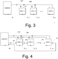
- Fig. 3 illustrates a system according to an embodiment.
- the phased array system of Fig. 3 will be described referring to the previous explanations for Figs. 1A, 1B and 2 .
- the phased array system of Fig. 3 comprises a controller 30 and a plurality of RFICs 31_1, 31_2, ..., 31_m, collectively referred to as RFICs 31.
- Each RFIC may be implemented as shown for RFIC 20 in Fig. 2 and has one or more antennas associated therewith, as also explained with reference to Fig. 2 .
- Controller 30 is coupled to RFICs 31 via a bus.
- a bus In Fig. 3 , as an example a two-line bus 32A, 32B is shown.
- the bus may be implemented based on any conventional bus standard, for example as an I2C bus, SPI bus, SCI bus, MIPI bus, CAN bus or any other suitable parallel or serial bus, and may also comprise more lines than explicitly shown.
- Bus 32A, 32B in a particular implementation may for example be an SPI bus clocked at about 50 MHz, but is not limited thereto.
- controller 30 broadcasts the common information explained already with respect to Fig. 2 , for example beamforming direction information or address information, to all RFICs 31.
- RFICs 31 then determine the respective phase, amplitude or delay settings based on this common information and chip specific stored information, as also explained referring to Fig. 2 .
- a two-line bus as shown in Fig. 3 is sufficient. It should be noted that nevertheless more lines may be provided, for example select lines for selecting individual RFICs, or read/write lines for determining a direction of communication, depending on a particular bus implementation.
- controller 30 is bus master and may communicate to all RFICs which act as bus slaves, but RFICs 31 may not directly communicate between each other. In other embodiments, such a direct communication between RFICs may also be possible, depending on a bus implementation. While a serial bus scheme is shown in Fig. 3 , in other embodiments parallel buses having a plurality of transmit or receive lines may be used.
- a minimum of lines required therefor may be two or three, depending on a bus system used, compared to over 100 lines for conventional solutions. Also, as in embodiments as discussed with reference to Figs. 2 and 3 comparatively little data, for example 32 bit or 20 bit, needs to be transmitted, the programming of the RFICs for a particular beamforming direction may be fast, for example significantly smaller than 1 ⁇ s for clock speeds smaller than 100 MHz.
- each RFIC 31 may also have an individual address by which it may be addressed by controller 30.
- one address indicates broadcasting, which is used to transmit the above-mentioned common information
- chip specific addresses are used to transmit chip specific information.
- individual addresses may be for example used for startup configuration, calibration or testing purposes like built-in test equipment (BITE) or built-in self-test (BIST). Therefore, a control command set for bus 32A, 32B may comprise broadcast commands which transmit common information to all RFICs as well as chip specific commands which address individual chips.
- the storage where the chip specific information is stored (for example storage 25 of Fig. 2 ) may be filled.
- the number of bits depends on an address space used. For example, a 20 bit address space may be used.
- Filling storage 25 in some implementations may occur when manufacturing the phased array system, and in other embodiments may be performed when booting the system.
- the antennas are coupled to respective RFICs which are coupled to a controller like controller 30.
- the RFICs together with the controller may be placed on a printed circuit board (PCB) and coupled to the controller via a bus also provided on the PCB.
- Antennas forming an antenna array may be provided also on the PCB or separately therefrom and connected to the respective associated RFIC.
- the positions of the antennas in the array coupled to each RFIC are fixed and may be programmed into storage 25. This programming may for example be performed by controller 30 using the above-mentioned chip specific addresses.
- the addresses of the individual RFICs need to be determined. Several possibilities may be used for this in various embodiments.
- RFICs may be provided with individual chip IDs when manufacturing.
- RFICs may be provided with a unique identifier (for example 48bit) using e-fuses.
- This chip ID may then be used for addressing the chips.
- a further possibility to provide addresses is to provide such addresses by hard coded wiring or soldering of pull-up or pull-down resistors on the printed circuit board for each RFIC.
- the RFIC needs corresponding additional balls/pins to be connected to such hard-coded wiring or pull-up/pull-down resistors.
- each RFIC is assigned an address by hardware coded on the printed circuit board.
- FIG. 4 A further possibility is to use an additional daisy chain bus for address initialization.
- a system is shown in Fig. 4 .
- the system of Fig. 4 is based on the system of Fig. 3 , and like elements bear the same reference numerals and will not be described repeatedly.
- the embodiment of Fig. 4 comprises bus 32A, 32B, which may for example be an SPI bus as mentioned.
- Fig. 4 comprises a second bus 40 in a daisy chain configuration.
- Second bus 40 may be an additional SPI bus, and may share some lines like a clock line and a CSN (chip select) line (not shown in Fig. 4 ) with bus 32A, 32B.
- Bus 40 may run at a lower clock frequency than bus 32A, 32B, for example at approximately 1 MHz or below.
- the addresses of RFICs 31 may be determined. For example, if already programmed internal addresses of RFICs 31 are used, controller 30 sends a first address request, which is replied to by RFIC 31 1 with its address. Then, controller 30 transmits a next address request via daisy chain bus 40.
- RFIC 31_1 As RFIC 31_1 has already responded to such a request, it now forwards the request to the next RFIC, 31_2, which then responds with its address. This is continued until all RFICs have provided their respective address to controller 30. Then, the storage of RFICs 31 may be individually filled using bus 32A, 32B and the individual addresses. In other embodiments, instead of using already preprogrammed addresses, the addresses may be provided by controller 30 in a similar manner. In this case, controller 30 transmits a first address via bus 40, which is adopted by RFIC 31_1. Then, a next address is sent via bus 40. As RFIC 31_1 has already adopted an address, it forwards the address to the next RFIC 31_2 which then adopts this address etc., until all RFICs are provided with an address.
- Fig. 4 requires an additional bus, but allows for greater flexibility as the addresses may be programmable.
- the addresses determined or provided may be then stored in a non-volatile memory like a flash memory in controller 30 and/or RFICs 31, such that the addressing procedure may need be performed only once and not at every startup.
- data written to the storage associated with each RFIC may be stored in a non-volatile memory so that the programming does not need to be performed at every booting.
- volatile memories may be used, and the storage may be programmed at each booting.
- Fig. 5 is a flowchart illustrating a method according to some embodiments, using the techniques as discussed above. To avoid repetitions, the method of Fig. 5 will be explained by referring to the embodiments of Figs. 1-4 described above. However, the method of Fig. 5 may also be implemented in other devices and systems than the ones shown in Figs. 1-4 above.
- an initialization is performed, where storages associated with RFICs are filled (for example storage 25 of Fig. 2 ).
- This initialization may be performed once at the manufacturer or may be performed repeatedly, for example when booting a phased array system.
- positions of antennas associated with the respective RFICs may be written into the storage, or phase, delay and/or amplitude information may be written into the storage for a plurality of different beamforming directions.
- common information is broadcasted to a plurality of RFICs, for example from controller 30 to RFICs 31 of Fig. 3 .
- the common information may comprise beamforming direction information or may comprise a storage address associated with a particular beamforming direction.
- the method comprises determining delay, phase and/or amplitude settings in each RFIC based on the common information and chip specific information stored in the storage, as explained above.
- the method comprises applying the settings determined at 52 for transmitting and/or receiving radio frequency waves via a plurality of antennas.
- Example 1 A phased array system, comprising:
- Example 2 The system of example 1, wherein the associated storage is included in the radio frequency integrated circuits.
- Example 3 The system of example 1 or 2, wherein the associated storage comprises a static random access memory or an e-fuse.
- Example 4 The system of any one of examples 1 to 3, wherein the common information comprises beamforming direction information, and wherein the chip specific information comprises position information of antennas associated with the respective radio frequency integrated circuit, wherein each of the radio frequency integrated circuits is configured to calculate the at least one of the phase, delay or amplitude settings based on the position information and the beamforming direction information.
- Example 5 The system of any one of examples 1 to 3, wherein the common information includes address information, and wherein the chip specific information includes a plurality of stored phase, delay or amplitude settings, wherein each radio frequency integrated circuit is configured to retrieve at least one of the phase, delay or amplitude settings based on the address information from the associated storage.
- Example 6 The system of any one of examples 1-5, wherein the common information selects between using phase settings and using delay settings.
- Example 7 The system of any one of examples 1-6, wherein the common information comprises frequency information indicating a frequency to be used for transmitting and/or receiving by the radio frequency integrated circuits.
- Example 8 The system of any one of examples 1-7, wherein the chip specific information comprises chip specific calibration information.
- Example 9 The system of any one of examples 1-8, further comprising a bus coupling the controller to each of the radio frequency integrated circuits, wherein the controller is configured to broadcast the common information via the bus.
- Example 10 The system of example 9, wherein the bus comprises a serial bus.
- Example 11 The phased array system of any one of examples 1-10, wherein the controller is configured to provide the chip specific information to the radio frequency integrated circuits during an initialization phase.
- Example 12 The system of example 11, wherein the controller is provided to provide the chip specific information using individual addressing of the radio frequency integrated circuits via the bus.
- Example 13 The system of any one of examples 8-11, wherein the system comprises an additional bus coupling the radio frequency integrated circuits in a daisy chain configuration, wherein the controller is configured to determine addresses of the radio frequency integrated circuits using the additional bus.
- Example 14 A radio frequency integrated circuit, comprising:
- Example 15 The radio frequency integrated circuit of example 14, further comprising the associated storage.
- Example 16 The radio frequency integrated circuit of example 14 or 15, wherein the common information comprises beamforming direction information, and wherein the chip specific information comprises position information of antennas associated with the respective radio frequency integrated circuit, wherein the logic circuit is configured to calculate the at least one of the phase, delay or amplitude settings based on the position information and the beamforming direction information.
- Example 17 The radio frequency integrated circuit of example 14 or 15, wherein the common information includes address information, and wherein the chip specific information includes a plurality of stored phase, delay or amplitude settings, wherein the logic circuit is configured to retrieve the phase, delay or amplitude setting based on the address information from the associated storage.
- Example 18 The radio frequency integrated circuit of any one of examples 14-17, wherein the chip specific information comprises chip specific calibration information.
- Example 19 The radio frequency circuit of any one of examples 14-18, wherein the first interface is a serial bus interface.
- Example 20 The radio frequency circuit of any one of examples 14-19, wherein the common information comprises frequency information indicating a frequency to be used for transmitting and/or receiving by the radio frequency integrated circuit.
- Example 21 A method, comprising:
- Example 22 The method of example 21, wherein the common information comprises beamforming direction information, and wherein the chip specific information comprises position information of antennas associated with the respective radio frequency integrated circuit, wherein the method further comprises: calculating, in each radio frequency integrated circuit, the at least one of the phase, delay or amplitude settings based on the position information and the beamforming direction information.
- Example 23 The method of example 21, wherein the common information includes address information, and wherein the chip specific information includes a plurality of stored phase, delay or amplitude settings, wherein the method further comprises: retrieving, in each radio frequency integrated circuit, the phase, delay or amplitude setting based on the address information.
- Example 24 The method of any one of examples 21-23, further comprising selecting between using phase settings and using delay settings based on the common information.
- Example 25 The method of any one of examples 21-24, wherein the chip specific information comprises chip specific calibration information.
- Example 26 The method of any one of examples 21-24, further comprising providing the chip specific information to the radio frequency integrated circuits during an initialization phase.
Landscapes
- Engineering & Computer Science (AREA)
- Computer Networks & Wireless Communication (AREA)
- Signal Processing (AREA)
- Variable-Direction Aerials And Aerial Arrays (AREA)
Priority Applications (1)
| Application Number | Priority Date | Filing Date | Title |
|---|---|---|---|
| EP18208827.8A EP3661075A1 (de) | 2018-11-28 | 2018-11-28 | Phasengesteuertes arraysystem, integrierte hochfrequenzschaltung und entsprechendes verfahren |
Applications Claiming Priority (1)
| Application Number | Priority Date | Filing Date | Title |
|---|---|---|---|
| EP18208827.8A EP3661075A1 (de) | 2018-11-28 | 2018-11-28 | Phasengesteuertes arraysystem, integrierte hochfrequenzschaltung und entsprechendes verfahren |
Publications (1)
| Publication Number | Publication Date |
|---|---|
| EP3661075A1 true EP3661075A1 (de) | 2020-06-03 |
Family
ID=64556740
Family Applications (1)
| Application Number | Title | Priority Date | Filing Date |
|---|---|---|---|
| EP18208827.8A Withdrawn EP3661075A1 (de) | 2018-11-28 | 2018-11-28 | Phasengesteuertes arraysystem, integrierte hochfrequenzschaltung und entsprechendes verfahren |
Country Status (1)
| Country | Link |
|---|---|
| EP (1) | EP3661075A1 (de) |
Cited By (3)
| Publication number | Priority date | Publication date | Assignee | Title |
|---|---|---|---|---|
| WO2024107485A1 (en) * | 2022-11-14 | 2024-05-23 | Qualcomm Incorporated | Radio frequency integrated circuit (rfic) selection |
| US12417203B1 (en) | 2024-05-17 | 2025-09-16 | Rockwell Collins, Inc. | High speed, extensible and self-healing data network for AESA RFIC arrays |
| DE102024131310A1 (de) | 2024-09-09 | 2026-03-12 | GM Global Technology Operations LLC | Serielle gruppen-id-adresse für aktive/abstimmbare fahrzeugantennen |
Citations (3)
| Publication number | Priority date | Publication date | Assignee | Title |
|---|---|---|---|---|
| US20140210668A1 (en) * | 2013-01-28 | 2014-07-31 | Tubis Technology | Hierarchically Elaborated Phased-Array Antenna Modules and Faster Beam Steering Method of Operation. |
| WO2016099691A1 (en) * | 2014-12-17 | 2016-06-23 | Qualcomm Incorporated | Programming hardware registers using a pipelined register bus, and related methods, systems, and apparatuses |
| US9478858B1 (en) * | 2013-02-28 | 2016-10-25 | Rockwell Collins, Inc. | Multi-chip module architecture |
-
2018
- 2018-11-28 EP EP18208827.8A patent/EP3661075A1/de not_active Withdrawn
Patent Citations (3)
| Publication number | Priority date | Publication date | Assignee | Title |
|---|---|---|---|---|
| US20140210668A1 (en) * | 2013-01-28 | 2014-07-31 | Tubis Technology | Hierarchically Elaborated Phased-Array Antenna Modules and Faster Beam Steering Method of Operation. |
| US9478858B1 (en) * | 2013-02-28 | 2016-10-25 | Rockwell Collins, Inc. | Multi-chip module architecture |
| WO2016099691A1 (en) * | 2014-12-17 | 2016-06-23 | Qualcomm Incorporated | Programming hardware registers using a pipelined register bus, and related methods, systems, and apparatuses |
Cited By (3)
| Publication number | Priority date | Publication date | Assignee | Title |
|---|---|---|---|---|
| WO2024107485A1 (en) * | 2022-11-14 | 2024-05-23 | Qualcomm Incorporated | Radio frequency integrated circuit (rfic) selection |
| US12417203B1 (en) | 2024-05-17 | 2025-09-16 | Rockwell Collins, Inc. | High speed, extensible and self-healing data network for AESA RFIC arrays |
| DE102024131310A1 (de) | 2024-09-09 | 2026-03-12 | GM Global Technology Operations LLC | Serielle gruppen-id-adresse für aktive/abstimmbare fahrzeugantennen |
Similar Documents
| Publication | Publication Date | Title |
|---|---|---|
| US11276939B2 (en) | Phased array antenna system including a modular control and monitoring architecture | |
| US11057088B2 (en) | Hierarchically elaborated phased-array antenna modules and faster beam steering method of operation | |
| US10686258B2 (en) | Hard-wired address for phased array antenna panels | |
| US10644400B2 (en) | Hierarchically elaborated phased-array antenna modules and faster beam steering method of operation by a host processor | |
| US9264039B2 (en) | Circuit and method for on-die termination, and semiconductor memory device including the same | |
| US10361699B2 (en) | Memory modules, memory systems including the same, and methods of calibrating multi-die impedance of the memory modules | |
| US10354703B2 (en) | Semiconductor device and system performing calibration operation | |
| US10320093B2 (en) | Phased array control circuit | |
| EP3661075A1 (de) | Phasengesteuertes arraysystem, integrierte hochfrequenzschaltung und entsprechendes verfahren | |
| JP4920039B2 (ja) | ニブル・デスキュー方法、装置、及びシステム | |
| US10750377B1 (en) | Multi-mode control with fast-access lookup table implementation | |
| EP2009553B1 (de) | Reduzierte Signalpegelunterstützung für Speichergeräte | |
| EP4328918B1 (de) | Einzelschleifenspeichervorrichtung, doppelschleifenspeichervorrichtung und zq-kalibrierungsverfahren | |
| US10734041B2 (en) | Semiconductor apparatus related to termination and semiconductor system including the semiconductor apparatus | |
| US10637471B1 (en) | Termination circuit and semiconductor apparatus including the termination circuit | |
| US7991020B2 (en) | Quad rate transmitter equalization | |
| JPH07115317A (ja) | 電子走査アンテナ |
Legal Events
| Date | Code | Title | Description |
|---|---|---|---|
| PUAI | Public reference made under article 153(3) epc to a published international application that has entered the european phase |
Free format text: ORIGINAL CODE: 0009012 |
|
| STAA | Information on the status of an ep patent application or granted ep patent |
Free format text: STATUS: THE APPLICATION HAS BEEN PUBLISHED |
|
| AK | Designated contracting states |
Kind code of ref document: A1 Designated state(s): AL AT BE BG CH CY CZ DE DK EE ES FI FR GB GR HR HU IE IS IT LI LT LU LV MC MK MT NL NO PL PT RO RS SE SI SK SM TR |
|
| AX | Request for extension of the european patent |
Extension state: BA ME |
|
| STAA | Information on the status of an ep patent application or granted ep patent |
Free format text: STATUS: THE APPLICATION IS DEEMED TO BE WITHDRAWN |
|
| 18D | Application deemed to be withdrawn |
Effective date: 20201204 |