EP3661009A1 - Detection of shoot-through in power converters - Google Patents
Detection of shoot-through in power converters Download PDFInfo
- Publication number
- EP3661009A1 EP3661009A1 EP19208691.6A EP19208691A EP3661009A1 EP 3661009 A1 EP3661009 A1 EP 3661009A1 EP 19208691 A EP19208691 A EP 19208691A EP 3661009 A1 EP3661009 A1 EP 3661009A1
- Authority
- EP
- European Patent Office
- Prior art keywords
- shoot
- capacitor
- voltage value
- voltage
- condition
- Prior art date
- Legal status (The legal status is an assumption and is not a legal conclusion. Google has not performed a legal analysis and makes no representation as to the accuracy of the status listed.)
- Granted
Links
- 238000001514 detection method Methods 0.000 title claims description 21
- 239000003990 capacitor Substances 0.000 claims abstract description 154
- 238000000034 method Methods 0.000 claims description 42
- 230000003111 delayed effect Effects 0.000 claims description 17
- 230000000116 mitigating effect Effects 0.000 claims description 7
- 230000004044 response Effects 0.000 claims description 4
- 239000004065 semiconductor Substances 0.000 description 25
- 230000008569 process Effects 0.000 description 24
- 230000000903 blocking effect Effects 0.000 description 13
- 230000001105 regulatory effect Effects 0.000 description 8
- 238000005259 measurement Methods 0.000 description 6
- 230000001276 controlling effect Effects 0.000 description 5
- 238000010586 diagram Methods 0.000 description 4
- 230000003750 conditioning effect Effects 0.000 description 3
- 230000007423 decrease Effects 0.000 description 3
- 230000009471 action Effects 0.000 description 2
- 230000004075 alteration Effects 0.000 description 2
- 238000006243 chemical reaction Methods 0.000 description 2
- 238000012937 correction Methods 0.000 description 2
- 238000013461 design Methods 0.000 description 2
- 238000007599 discharging Methods 0.000 description 2
- 238000004146 energy storage Methods 0.000 description 2
- 230000006872 improvement Effects 0.000 description 2
- 238000012986 modification Methods 0.000 description 2
- 230000004048 modification Effects 0.000 description 2
- 230000002730 additional effect Effects 0.000 description 1
- 230000001143 conditioned effect Effects 0.000 description 1
- 238000010276 construction Methods 0.000 description 1
- 230000008030 elimination Effects 0.000 description 1
- 238000003379 elimination reaction Methods 0.000 description 1
- 230000001747 exhibiting effect Effects 0.000 description 1
- 230000005669 field effect Effects 0.000 description 1
- 230000006870 function Effects 0.000 description 1
- 230000007774 longterm Effects 0.000 description 1
- 238000004519 manufacturing process Methods 0.000 description 1
- 230000007935 neutral effect Effects 0.000 description 1
- 238000012545 processing Methods 0.000 description 1
Images


Classifications
-
- H—ELECTRICITY
- H02—GENERATION; CONVERSION OR DISTRIBUTION OF ELECTRIC POWER
- H02M—APPARATUS FOR CONVERSION BETWEEN AC AND AC, BETWEEN AC AND DC, OR BETWEEN DC AND DC, AND FOR USE WITH MAINS OR SIMILAR POWER SUPPLY SYSTEMS; CONVERSION OF DC OR AC INPUT POWER INTO SURGE OUTPUT POWER; CONTROL OR REGULATION THEREOF
- H02M1/00—Details of apparatus for conversion
- H02M1/08—Circuits specially adapted for the generation of control voltages for semiconductor devices incorporated in static converters
-
- H—ELECTRICITY
- H02—GENERATION; CONVERSION OR DISTRIBUTION OF ELECTRIC POWER
- H02H—EMERGENCY PROTECTIVE CIRCUIT ARRANGEMENTS
- H02H7/00—Emergency protective circuit arrangements specially adapted for specific types of electric machines or apparatus or for sectionalised protection of cable or line systems, and effecting automatic switching in the event of an undesired change from normal working conditions
- H02H7/10—Emergency protective circuit arrangements specially adapted for specific types of electric machines or apparatus or for sectionalised protection of cable or line systems, and effecting automatic switching in the event of an undesired change from normal working conditions for converters; for rectifiers
- H02H7/12—Emergency protective circuit arrangements specially adapted for specific types of electric machines or apparatus or for sectionalised protection of cable or line systems, and effecting automatic switching in the event of an undesired change from normal working conditions for converters; for rectifiers for static converters or rectifiers
- H02H7/122—Emergency protective circuit arrangements specially adapted for specific types of electric machines or apparatus or for sectionalised protection of cable or line systems, and effecting automatic switching in the event of an undesired change from normal working conditions for converters; for rectifiers for static converters or rectifiers for inverters, i.e. dc/ac converters
- H02H7/1225—Emergency protective circuit arrangements specially adapted for specific types of electric machines or apparatus or for sectionalised protection of cable or line systems, and effecting automatic switching in the event of an undesired change from normal working conditions for converters; for rectifiers for static converters or rectifiers for inverters, i.e. dc/ac converters responsive to internal faults, e.g. shoot-through
-
- G—PHYSICS
- G01—MEASURING; TESTING
- G01R—MEASURING ELECTRIC VARIABLES; MEASURING MAGNETIC VARIABLES
- G01R31/00—Arrangements for testing electric properties; Arrangements for locating electric faults; Arrangements for electrical testing characterised by what is being tested not provided for elsewhere
- G01R31/12—Testing dielectric strength or breakdown voltage ; Testing or monitoring effectiveness or level of insulation, e.g. of a cable or of an apparatus, for example using partial discharge measurements; Electrostatic testing
- G01R31/1227—Testing dielectric strength or breakdown voltage ; Testing or monitoring effectiveness or level of insulation, e.g. of a cable or of an apparatus, for example using partial discharge measurements; Electrostatic testing of components, parts or materials
- G01R31/1263—Testing dielectric strength or breakdown voltage ; Testing or monitoring effectiveness or level of insulation, e.g. of a cable or of an apparatus, for example using partial discharge measurements; Electrostatic testing of components, parts or materials of solid or fluid materials, e.g. insulation films, bulk material; of semiconductors or LV electronic components or parts; of cable, line or wire insulation
- G01R31/129—Testing dielectric strength or breakdown voltage ; Testing or monitoring effectiveness or level of insulation, e.g. of a cable or of an apparatus, for example using partial discharge measurements; Electrostatic testing of components, parts or materials of solid or fluid materials, e.g. insulation films, bulk material; of semiconductors or LV electronic components or parts; of cable, line or wire insulation of components or parts made of semiconducting materials; of LV components or parts
-
- G—PHYSICS
- G01—MEASURING; TESTING
- G01R—MEASURING ELECTRIC VARIABLES; MEASURING MAGNETIC VARIABLES
- G01R19/00—Arrangements for measuring currents or voltages or for indicating presence or sign thereof
- G01R19/04—Measuring peak values or amplitude or envelope of ac or of pulses
-
- G—PHYSICS
- G01—MEASURING; TESTING
- G01R—MEASURING ELECTRIC VARIABLES; MEASURING MAGNETIC VARIABLES
- G01R19/00—Arrangements for measuring currents or voltages or for indicating presence or sign thereof
- G01R19/10—Measuring sum, difference or ratio
-
- G—PHYSICS
- G01—MEASURING; TESTING
- G01R—MEASURING ELECTRIC VARIABLES; MEASURING MAGNETIC VARIABLES
- G01R31/00—Arrangements for testing electric properties; Arrangements for locating electric faults; Arrangements for electrical testing characterised by what is being tested not provided for elsewhere
- G01R31/40—Testing power supplies
- G01R31/42—AC power supplies
-
- H—ELECTRICITY
- H02—GENERATION; CONVERSION OR DISTRIBUTION OF ELECTRIC POWER
- H02H—EMERGENCY PROTECTIVE CIRCUIT ARRANGEMENTS
- H02H7/00—Emergency protective circuit arrangements specially adapted for specific types of electric machines or apparatus or for sectionalised protection of cable or line systems, and effecting automatic switching in the event of an undesired change from normal working conditions
- H02H7/10—Emergency protective circuit arrangements specially adapted for specific types of electric machines or apparatus or for sectionalised protection of cable or line systems, and effecting automatic switching in the event of an undesired change from normal working conditions for converters; for rectifiers
- H02H7/12—Emergency protective circuit arrangements specially adapted for specific types of electric machines or apparatus or for sectionalised protection of cable or line systems, and effecting automatic switching in the event of an undesired change from normal working conditions for converters; for rectifiers for static converters or rectifiers
- H02H7/1216—Emergency protective circuit arrangements specially adapted for specific types of electric machines or apparatus or for sectionalised protection of cable or line systems, and effecting automatic switching in the event of an undesired change from normal working conditions for converters; for rectifiers for static converters or rectifiers for AC-AC converters
-
- H—ELECTRICITY
- H02—GENERATION; CONVERSION OR DISTRIBUTION OF ELECTRIC POWER
- H02J—CIRCUIT ARRANGEMENTS OR SYSTEMS FOR SUPPLYING OR DISTRIBUTING ELECTRIC POWER; SYSTEMS FOR STORING ELECTRIC ENERGY
- H02J9/00—Circuit arrangements for emergency or stand-by power supply, e.g. for emergency lighting
- H02J9/04—Circuit arrangements for emergency or stand-by power supply, e.g. for emergency lighting in which the distribution system is disconnected from the normal source and connected to a standby source
- H02J9/06—Circuit arrangements for emergency or stand-by power supply, e.g. for emergency lighting in which the distribution system is disconnected from the normal source and connected to a standby source with automatic change-over, e.g. UPS systems
- H02J9/062—Circuit arrangements for emergency or stand-by power supply, e.g. for emergency lighting in which the distribution system is disconnected from the normal source and connected to a standby source with automatic change-over, e.g. UPS systems for AC powered loads
-
- H—ELECTRICITY
- H02—GENERATION; CONVERSION OR DISTRIBUTION OF ELECTRIC POWER
- H02M—APPARATUS FOR CONVERSION BETWEEN AC AND AC, BETWEEN AC AND DC, OR BETWEEN DC AND DC, AND FOR USE WITH MAINS OR SIMILAR POWER SUPPLY SYSTEMS; CONVERSION OF DC OR AC INPUT POWER INTO SURGE OUTPUT POWER; CONTROL OR REGULATION THEREOF
- H02M1/00—Details of apparatus for conversion
- H02M1/32—Means for protecting converters other than automatic disconnection
- H02M1/325—Means for protecting converters other than automatic disconnection with means for allowing continuous operation despite a fault, i.e. fault tolerant converters
-
- H—ELECTRICITY
- H02—GENERATION; CONVERSION OR DISTRIBUTION OF ELECTRIC POWER
- H02M—APPARATUS FOR CONVERSION BETWEEN AC AND AC, BETWEEN AC AND DC, OR BETWEEN DC AND DC, AND FOR USE WITH MAINS OR SIMILAR POWER SUPPLY SYSTEMS; CONVERSION OF DC OR AC INPUT POWER INTO SURGE OUTPUT POWER; CONTROL OR REGULATION THEREOF
- H02M1/00—Details of apparatus for conversion
- H02M1/38—Means for preventing simultaneous conduction of switches
-
- H—ELECTRICITY
- H02—GENERATION; CONVERSION OR DISTRIBUTION OF ELECTRIC POWER
- H02M—APPARATUS FOR CONVERSION BETWEEN AC AND AC, BETWEEN AC AND DC, OR BETWEEN DC AND DC, AND FOR USE WITH MAINS OR SIMILAR POWER SUPPLY SYSTEMS; CONVERSION OF DC OR AC INPUT POWER INTO SURGE OUTPUT POWER; CONTROL OR REGULATION THEREOF
- H02M5/00—Conversion of ac power input into ac power output, e.g. for change of voltage, for change of frequency, for change of number of phases
- H02M5/40—Conversion of ac power input into ac power output, e.g. for change of voltage, for change of frequency, for change of number of phases with intermediate conversion into dc
- H02M5/42—Conversion of ac power input into ac power output, e.g. for change of voltage, for change of frequency, for change of number of phases with intermediate conversion into dc by static converters
- H02M5/44—Conversion of ac power input into ac power output, e.g. for change of voltage, for change of frequency, for change of number of phases with intermediate conversion into dc by static converters using discharge tubes or semiconductor devices to convert the intermediate dc into ac
- H02M5/453—Conversion of ac power input into ac power output, e.g. for change of voltage, for change of frequency, for change of number of phases with intermediate conversion into dc by static converters using discharge tubes or semiconductor devices to convert the intermediate dc into ac using devices of a triode or transistor type requiring continuous application of a control signal
- H02M5/458—Conversion of ac power input into ac power output, e.g. for change of voltage, for change of frequency, for change of number of phases with intermediate conversion into dc by static converters using discharge tubes or semiconductor devices to convert the intermediate dc into ac using devices of a triode or transistor type requiring continuous application of a control signal using semiconductor devices only
- H02M5/4585—Conversion of ac power input into ac power output, e.g. for change of voltage, for change of frequency, for change of number of phases with intermediate conversion into dc by static converters using discharge tubes or semiconductor devices to convert the intermediate dc into ac using devices of a triode or transistor type requiring continuous application of a control signal using semiconductor devices only having a rectifier with controlled elements
-
- H—ELECTRICITY
- H02—GENERATION; CONVERSION OR DISTRIBUTION OF ELECTRIC POWER
- H02M—APPARATUS FOR CONVERSION BETWEEN AC AND AC, BETWEEN AC AND DC, OR BETWEEN DC AND DC, AND FOR USE WITH MAINS OR SIMILAR POWER SUPPLY SYSTEMS; CONVERSION OF DC OR AC INPUT POWER INTO SURGE OUTPUT POWER; CONTROL OR REGULATION THEREOF
- H02M7/00—Conversion of ac power input into dc power output; Conversion of dc power input into ac power output
- H02M7/42—Conversion of dc power input into ac power output without possibility of reversal
- H02M7/44—Conversion of dc power input into ac power output without possibility of reversal by static converters
- H02M7/48—Conversion of dc power input into ac power output without possibility of reversal by static converters using discharge tubes with control electrode or semiconductor devices with control electrode
- H02M7/53—Conversion of dc power input into ac power output without possibility of reversal by static converters using discharge tubes with control electrode or semiconductor devices with control electrode using devices of a triode or transistor type requiring continuous application of a control signal
- H02M7/537—Conversion of dc power input into ac power output without possibility of reversal by static converters using discharge tubes with control electrode or semiconductor devices with control electrode using devices of a triode or transistor type requiring continuous application of a control signal using semiconductor devices only, e.g. single switched pulse inverters
-
- H—ELECTRICITY
- H02—GENERATION; CONVERSION OR DISTRIBUTION OF ELECTRIC POWER
- H02M—APPARATUS FOR CONVERSION BETWEEN AC AND AC, BETWEEN AC AND DC, OR BETWEEN DC AND DC, AND FOR USE WITH MAINS OR SIMILAR POWER SUPPLY SYSTEMS; CONVERSION OF DC OR AC INPUT POWER INTO SURGE OUTPUT POWER; CONTROL OR REGULATION THEREOF
- H02M1/00—Details of apparatus for conversion
- H02M1/42—Circuits or arrangements for compensating for or adjusting power factor in converters or inverters
- H02M1/4208—Arrangements for improving power factor of AC input
- H02M1/4216—Arrangements for improving power factor of AC input operating from a three-phase input voltage
-
- H—ELECTRICITY
- H02—GENERATION; CONVERSION OR DISTRIBUTION OF ELECTRIC POWER
- H02M—APPARATUS FOR CONVERSION BETWEEN AC AND AC, BETWEEN AC AND DC, OR BETWEEN DC AND DC, AND FOR USE WITH MAINS OR SIMILAR POWER SUPPLY SYSTEMS; CONVERSION OF DC OR AC INPUT POWER INTO SURGE OUTPUT POWER; CONTROL OR REGULATION THEREOF
- H02M7/00—Conversion of ac power input into dc power output; Conversion of dc power input into ac power output
- H02M7/42—Conversion of dc power input into ac power output without possibility of reversal
- H02M7/44—Conversion of dc power input into ac power output without possibility of reversal by static converters
- H02M7/48—Conversion of dc power input into ac power output without possibility of reversal by static converters using discharge tubes with control electrode or semiconductor devices with control electrode
- H02M7/483—Converters with outputs that each can have more than two voltages levels
Definitions
- UPSs Uninterruptible Power Supplies
- Known UPSs include online UPSs, offline UPSs, line-interactive UPSs, as well as others.
- Online UPSs provide conditioned AC power as well as back-up AC power upon interruption of a primary source of AC power.
- Offline UPSs typically do not provide conditioning of input AC power, but do provide back-up AC power upon interruption of the primary AC power source.
- Line-interactive UPSs are similar to offline UPSs in that they switch to battery power when a blackout occurs but also typically include a multi-tap transformer for regulating the output voltage provided by the UPS.
- the shoot-through detector further comprises a peak detection and hold circuit configured to receive the first voltage, detect a peak of the first voltage, and hold the peak of the first voltage, the peak of the first voltage corresponding to the first voltage value.
- the UPS system further includes a controller coupled to the shoot-through detector, wherein the shoot-through detector is further configured to provide the output signal to the controller, and wherein the controller is configured to control at least one switching device coupled to the at least one capacitor to be in an open and non-conducting position in response to receiving the output signal.
- obtaining the second voltage value includes obtaining the second voltage value after a delay period from a time at which the first voltage value is obtained.
- the method further includes mitigating, responsive to outputting the output signal, the shoot-through condition.
- mitigating the shoot-through condition includes controlling at least one switching device coupled with the capacitor to be in an open and non-conducting state.
- determining that the capacitor is experiencing a shoot-through condition includes determining that the second voltage value exceeds the first voltage value by at least a threshold amount for a threshold period of time.
- Certain power devices such as Uninterruptible Power Supplies (UPSs) may include power conditioning circuitry.
- the power conditioning circuitry may include two or more semiconductor switching devices coupled in series with a capacitor. If the semiconductors are simultaneously turned on or if a conductive path through the semiconductors is otherwise available, the capacitor may rapidly discharge through the semiconductors in a phenomenon known in the art as "shoot-through.” Shoot-through may be considered disadvantageous in certain situations as it can damage one or more components in the UPS.
- Shoot-through may occur intentionally or unintentionally.
- unintentional shoot-through may be caused by a faulty semiconductor device, gate driver, or control signal.
- many semiconductors are rated to withstand shoot-through for several microseconds, during which time the current through the semiconductor is limited by the saturation of the semiconductors, inadvertent shoot-through may nonetheless be considered disadvantageous at least in part because of voltage stress placed on various components. Accordingly, it may be advantageous to be able to detect and mitigate shoot-through without substantially increasing the size and cost of the power device in which the at least one capacitor is implemented.
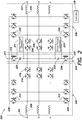
- FIG. 1 illustrates a conventional three-level inverter 100.
- the inverter 100 may be implemented in an Uninterruptible Power Supply (UPS), for example.
- the inverter 100 includes a first DC capacitor 102, a second DC capacitor 104, a first semiconductor 106, a second semiconductor 108, a third semiconductor 110, a fourth semiconductor 112, an inverter choke 114, and an output current sensor 116.
- UPS Uninterruptible Power Supply
- an advanced gate driver in combination with a voltage sensor is implemented to detect and mitigate shoot-through.
- the advanced gate driver may measure the voltage across the first semiconductor 106 and, if the voltage exceeds a preset threshold value (for example, approximately 7 V), the advanced gate driver may turn off the first semiconductor 106 to prevent or limit a current through the first semiconductor 106, thereby terminating the shoot-through condition.
- a preset threshold value for example, approximately 7 V
- advanced gate drivers may be costly, complex, and physically large, particularly as a number of semiconductors that need to be driven increases.
- a system is provided to detect and mitigate shoot-through without prohibitively increasing cost, complexity, and physical footprint.
- a relatively simple circuit is implemented to measure a capacitor voltage value, hold the measured voltage value, and compare the measured voltage value to a subsequently measured capacitor voltage value after a delay. Responsive to detecting a shoot-through condition based on the comparison of the delayed voltage value to the newly-measured voltage value, the circuit may be configured to turn off one or more semiconductors to prevent or mitigate the shoot-through condition.
- the first switch 210 and the second switch 212 are 1200V Insulated-Gate Bipolar Transistors (IGBT); however, in other embodiments, the switches 210, 212 may be rated differently or different types of switches may be utilized (for example, the switches 210, 212 can be replaced with diodes if uni-directional power conversion in the PFC portion 202 is sufficient).
- the ninth switch 230 and the tenth switch 232 are 1200V IGBTs; however, in other embodiments, the switches 230, 232 may be rated differently or different types of switches may be utilized.
- the third switch 214, fourth switch 216, seventh switch 226, and eighth switch 228 are 600V IGBTs; however, in other embodiments, the switches 214, 216, 226, 228 may be rated differently or different types of switches may be utilized.
- Each of the switches 210-216, 226-232 may include an internal diode coupled between its collector and emitter.
- the fifth switch 218 and sixth switch 224 are 600V Metal-Oxide-Semiconductor Field-Effect Transistors (MOSFETs); however, in other embodiments, the switches 218, 224 may be rated differently or different types of switches (for example, IGBTs) may be utilized. Where the switches 218, 224 are implemented as MOSFETs, each of the switches 218, 224 may include an internal diode coupled between its drain and source.
- the source of the fifth switch 218 is coupled to the first DC bus 238.
- the drain of the fifth switch 218 is coupled to the first capacitor 220.
- the first capacitor 220 is coupled to the drain of the fifth switch 218 at a first connection, and is coupled to the collector of the fourth switch 216, the second capacitor 222, and the collector of the seventh switch 226 at a second connection.
- the first capacitor 220 is further coupled in parallel with the first shoot-through detector 221.
- the second capacitor 222 is coupled to the first capacitor 220, the collector of the fourth switch 216, and the collector of the seventh switch 226 at a first connection, and is coupled to the source of the sixth switch 224 at a second connection.
- the second capacitor 222 is further configured to be coupled in parallel with the second shoot-through detector 223.
- the source of the sixth switch 224 is coupled to the second capacitor 222, and the drain of the sixth switch 224 is coupled to the second DC bus 240.
- the collector of the seventh switch 226 is coupled to the first capacitor 220, the collector of the fourth switch 216, and the second capacitor 222.
- the emitter of the seventh switch 226 is coupled to the emitter of the eighth switch 228.
- the emitter of the eighth switch 228 is coupled to the emitter of the seventh switch 226.
- the collector of the eighth switch 228 is coupled to the emitter of the ninth switch 230, the collector of the tenth switch 232, and the output inductor 234.
- the controller 236 is configured to be communicatively coupled to a respective control terminal of one or more of the switches 210, 212, 214, 216, 218, 224, 226, 228, 230, 232.
- the first DC bus 238 is coupled to the collector of the first switch 210, the source of the fifth switch 218, the collector of the ninth switch 230, and the first backup power supply node 217.
- the second DC bus 240 is coupled to the emitter of the second switch 212, the drain of the sixth switch 224, the emitter of the tenth switch 232, and the second backup power supply node 225.
- one phase of the three-phase input power may be received at the first input 201.
- the controller 236 operates the first switch 210 and the third switch 214 as a boost converter to convert the one phase of the three-phase input power into converted DC power.
- the controller 236 also operates the first switch 210 and the third switch 214 to provide power factor correction at the first input 201.
- the converted DC power is provided to the first DC bus 238.
- the ninth switch 230 is operated by the controller 236 to convert DC power from the first DC bus 238 into regulated AC power.
- the regulated AC power is provided to the first output 207 via the output inductor 234.
- the first shoot-through detector 221 may determine if the instantaneous voltage has continuously exceeded the delayed peak voltage measurement by more than a threshold amount for a threshold period of time.
- the threshold amount of time may be approximately 500 ns. If the instantaneous voltage has not continuously exceeded the delayed peak voltage measurement for a threshold amount of time (408 NO), then no shoot-through condition is detected (306 NO) and the process 400 ends by returning to 306 NO of the process 300. Otherwise (408 YES), the process 400 continues to act 410.
- a shoot-through detection signal is generated.
- the first shoot-through detector 221 may generate a signal indicating that the first capacitor 220 is experiencing a shoot-through condition (306 YES). The process 400 ends by returning to 306 YES of the process 300.
- the second input signal 538 may be implemented to provide a buffer value indicative of an amount by which the instantaneous voltage must exceed the delayed peak voltage for the shoot-through condition to be detected.
- the comparator 518 will output a signal indicating that a shoot-through condition is detected if, Vinstantaneous > Vpeak + Vbuffer where V instantaneous is a voltage measured at the non-inverting connection of the comparator 518, V peak is a most-recently-held peak voltage across the capacitor 502 held by the capacitor 532, and V buffer is a buffer voltage derived from the second input signal 538.
- one or more controllers may perform one or more of the operations discussed herein.
- the first shoot-through detector 221, the second shoot-through detector 223, the shoot-through detector 504, the controller 236, and the controller 612 are illustrated as discrete components, in some embodiments, a single controller may be configured to execute the functionality of each of the foregoing components.
- the controller 236 may be configured to execute the functionality of the shoot-through detectors 221, 223, 504, including detecting shoot-through in one or more capacitors.
- an embodiment of at least one of the shoot-through detectors 221, 223, 504 may be a component of the controller 236.
Landscapes
- Engineering & Computer Science (AREA)
- Power Engineering (AREA)
- Physics & Mathematics (AREA)
- General Physics & Mathematics (AREA)
- Business, Economics & Management (AREA)
- Emergency Management (AREA)
- Inverter Devices (AREA)
- Rectifiers (AREA)
Abstract
Description
- At least one example in accordance with the present invention relates generally to detecting and correcting semiconductor shoot-through in power converters.
- The use of power devices, such as Uninterruptible Power Supplies (UPSs), to provide regulated, uninterrupted power for sensitive and/or critical loads, such as computer systems and other data processing systems, is known. Known UPSs include online UPSs, offline UPSs, line-interactive UPSs, as well as others. Online UPSs provide conditioned AC power as well as back-up AC power upon interruption of a primary source of AC power. Offline UPSs typically do not provide conditioning of input AC power, but do provide back-up AC power upon interruption of the primary AC power source. Line-interactive UPSs are similar to offline UPSs in that they switch to battery power when a blackout occurs but also typically include a multi-tap transformer for regulating the output voltage provided by the UPS.
- According to at least one aspect of the present invention, an Uninterruptible Power Supply (UPS) system is provided including an input configured to receive input power, an interface configured to be coupled to a backup power supply and to receive backup power from the backup power supply, an output configured to provide output power derived from at least one of the input power and the backup power to a load, a power converter coupled to the input, at least one capacitor, and a shoot-through detector coupled to the at least one capacitor and being configured to: obtain a first voltage value indicative of a first voltage across the at least one capacitor, obtain a second voltage value indicative of a second voltage across the at least one capacitor, compare the first voltage value to the second voltage value, determine, based on the comparison, that the at least one capacitor is experiencing a shoot-through condition, and provide an output signal indicative of the shoot-through condition.
- In one embodiment, the shoot-through detector comprises a delay circuit configured to delay the first voltage value by a delay period to generate a delayed first voltage value. In some embodiments, the delay period is within a range of approximately 1-2 microseconds. In at least one embodiment, the shoot-through detector further comprises a comparator having: a first input configured to receive the delayed first voltage value, a second input configured to receive the second voltage value, and an output configured to output a signal indicative of a shoot-through condition responsive to determining that the second voltage value is greater than the first voltage value.
- In one embodiment, the shoot-through detector further comprises a logic circuit configured to: receive, from the output of the comparator, the output signal indicative of the shoot-through condition, and output, responsive to receiving the output signal for at least a threshold amount of time, a shoot-through signal indicative of the shoot-through condition. In an embodiment, the logic circuit is further configured to receive a parameter configuration value to set the threshold amount of time. In some embodiments, the threshold amount of time is approximately 500 nanoseconds.
- In at least one embodiment, the shoot-through detector further comprises a peak detection and hold circuit configured to receive the first voltage, detect a peak of the first voltage, and hold the peak of the first voltage, the peak of the first voltage corresponding to the first voltage value. In some embodiments, the UPS system further includes a controller coupled to the shoot-through detector, wherein the shoot-through detector is further configured to provide the output signal to the controller, and wherein the controller is configured to control at least one switching device coupled to the at least one capacitor to be in an open and non-conducting position in response to receiving the output signal.
- A method of detecting a shoot-through condition in a capacitor is provided, the method comprising acts of obtaining a first voltage value, the first voltage value being indicative of a first voltage across the capacitor, obtaining a second voltage value, the second voltage value being indicative of a second voltage across the capacitor, comparing the first voltage value to the second voltage value, determining, based on the comparison, that the capacitor is experiencing a shoot-through condition, and outputting an output signal indicative of the shoot-through condition.
- In an embodiment, obtaining the second voltage value includes obtaining the second voltage value after a delay period from a time at which the first voltage value is obtained. In at least one embodiment, the method further includes mitigating, responsive to outputting the output signal, the shoot-through condition. In some embodiments, mitigating the shoot-through condition includes controlling at least one switching device coupled with the capacitor to be in an open and non-conducting state. In at least one embodiment, determining that the capacitor is experiencing a shoot-through condition includes determining that the second voltage value exceeds the first voltage value by at least a threshold amount for a threshold period of time.
- In one embodiment, the method includes receiving, from a user, a configuration parameter corresponding to the threshold amount. In some embodiments, the method includes receiving, from a user, a configuration parameter corresponding to the threshold period of time. In at least one embodiment, the threshold period of time is approximately 500 nanoseconds. In an embodiment, obtaining the first voltage value includes detecting a peak of the first voltage and holding the peak of the first voltage.
- According to one aspect, an Uninterruptible Power Supply (UPS) system is provided comprising an input configured to receive input power, an output configured to provide output power to at least one load, at least one capacitor coupled to at least one switching device, and means for identifying, based on a first voltage across the at least one capacitor and a second voltage across the at least one capacitor, a shoot-through condition in the at least one capacitor. In one embodiment, the UPS system further includes means for operating the at least one switching device to mitigate the shoot-through condition.
- Various aspects of at least one embodiment are discussed below with reference to the accompanying figures, which are not intended to be drawn to scale. The figures are included to provide an illustration and a further understanding of the various aspects and embodiments, and are incorporated in and constitute a part of this specification, but are not intended as a definition of the limits of any particular embodiment. The drawings, together with the remainder of the specification, serve to explain principles and operations of the described and claimed aspects and embodiments. In the figures, each identical or nearly identical component that is illustrated in various figures is represented by a like numeral. For purposes of clarity, not every component may be labeled in every figure. In the figures:
-
FIG. 1 illustrates a conventional three-level inverter; -
FIG. 2 illustrates a three-level converter according to one embodiment; -
FIG. 3 illustrates a process of eliminating or mitigating capacitor shoot-through according to one embodiment; -
FIG. 4 illustrates a process of detecting capacitor shoot-through according to one embodiment; -
FIG. 5 illustrates a shoot-through detection circuit according to one embodiment; and -
FIG. 6 illustrates a block diagram of an uninterruptible power supply. - Examples of the methods and systems discussed herein are not limited in application to the details of construction and the arrangement of components set forth in the following description or illustrated in the accompanying drawings. The methods and systems are capable of implementation in other embodiments and of being practiced or of being carried out in various ways. Examples of specific implementations are provided herein for illustrative purposes only and are not intended to be limiting. In particular, acts, components, elements and features discussed in connection with any one or more examples are not intended to be excluded from a similar role in any other examples.
- Also, the phraseology and terminology used herein is for the purpose of description and should not be regarded as limiting. Any references to examples, embodiments, components, elements or acts of the systems and methods herein referred to in the singular may also embrace embodiments including a plurality, and any references in plural to any embodiment, component, element or act herein may also embrace embodiments including only a singularity. References in the singular or plural form are no intended to limit the presently disclosed systems or methods, their components, acts, or elements. The use herein of "including," "comprising," "having," "containing," "involving," and variations thereof is meant to encompass the items listed thereafter and equivalents thereof as well as additional items.
- References to "or" may be construed as inclusive so that any terms described using "or" may indicate any of a single, more than one, and all of the described terms. In addition, in the event of inconsistent usages of terms between this document and documents incorporated herein by reference, the term usage in the incorporated features is supplementary to that of this document; for irreconcilable differences, the term usage in this document controls.
- Certain power devices, such as Uninterruptible Power Supplies (UPSs), may include power conditioning circuitry. The power conditioning circuitry may include two or more semiconductor switching devices coupled in series with a capacitor. If the semiconductors are simultaneously turned on or if a conductive path through the semiconductors is otherwise available, the capacitor may rapidly discharge through the semiconductors in a phenomenon known in the art as "shoot-through." Shoot-through may be considered disadvantageous in certain situations as it can damage one or more components in the UPS.
- Shoot-through may occur intentionally or unintentionally. For example, unintentional shoot-through may be caused by a faulty semiconductor device, gate driver, or control signal. Although many semiconductors are rated to withstand shoot-through for several microseconds, during which time the current through the semiconductor is limited by the saturation of the semiconductors, inadvertent shoot-through may nonetheless be considered disadvantageous at least in part because of voltage stress placed on various components. Accordingly, it may be advantageous to be able to detect and mitigate shoot-through without substantially increasing the size and cost of the power device in which the at least one capacitor is implemented.
-
FIG. 1 illustrates a conventional three-level inverter 100. Theinverter 100 may be implemented in an Uninterruptible Power Supply (UPS), for example. Theinverter 100 includes afirst DC capacitor 102, asecond DC capacitor 104, afirst semiconductor 106, asecond semiconductor 108, athird semiconductor 110, afourth semiconductor 112, aninverter choke 114, and an outputcurrent sensor 116. - Shoot-through may occur in the
inverter 100 if thefirst DC capacitor 102 or thesecond DC capacitor 104 is short circuited. For example, if thefirst semiconductor 106 and thefourth semiconductor 112 are simultaneously turned on and conducting, thefirst DC capacitor 102 may discharge through a path including thefirst DC capacitor 102, thefirst semiconductor 106, thefourth semiconductor 112, and a diode coupled in parallel with thethird semiconductor 110. - In some conventional solutions, an advanced gate driver in combination with a voltage sensor is implemented to detect and mitigate shoot-through. For example, the advanced gate driver may measure the voltage across the
first semiconductor 106 and, if the voltage exceeds a preset threshold value (for example, approximately 7 V), the advanced gate driver may turn off thefirst semiconductor 106 to prevent or limit a current through thefirst semiconductor 106, thereby terminating the shoot-through condition. However, advanced gate drivers may be costly, complex, and physically large, particularly as a number of semiconductors that need to be driven increases. - In light of the foregoing, a system is provided to detect and mitigate shoot-through without prohibitively increasing cost, complexity, and physical footprint. A relatively simple circuit is implemented to measure a capacitor voltage value, hold the measured voltage value, and compare the measured voltage value to a subsequently measured capacitor voltage value after a delay. Responsive to detecting a shoot-through condition based on the comparison of the delayed voltage value to the newly-measured voltage value, the circuit may be configured to turn off one or more semiconductors to prevent or mitigate the shoot-through condition.
- At least one embodiment described herein is directed to a three-level Uninterruptible Power Supply (UPS) topology, the details of which are described in greater detail, for example, in
U.S. Patent Application No. 15/320,622 -
FIG. 2 is a schematic diagram of a three-level power converter 200 according to one embodiment described herein. The three-level inverter 200 includes three power conversion branches, each of which operates similarly in certain embodiments. For example, the three-level power converter 200 may be configured to receive three-phase power, and provide each phase of the three-phase power to a respective branch of the three branches. For clarity of illustration, certain components of a first branch of the three branches will be specifically identified. Other branches may include similar components which operate similarly. - The three-
level power converter 200 includes afirst input 201, a Power Factor Correction (PFC)portion 202, a Direct Current (DC) linkportion 204, aninverter portion 206, and afirst output 207. ThePFC portion 202 includes aninput inductor 208, afirst switch 210, asecond switch 212, athird switch 214, and afourth switch 216. TheDC link portion 204 includes a first backuppower supply node 217, afifth switch 218, afirst capacitor 220, a first shoot-throughdetector 221, asecond capacitor 222, a second shoot-throughdetector 223, asixth switch 224, and a second backuppower supply node 225. Theinverter portion 206 includes aseventh switch 226, aneighth switch 228, aninth switch 230, atenth switch 232, and anoutput inductor 234. ThePFC portion 202, theDC link portion 204, and theinverter portion 206 collectively include afirst DC bus 238 and asecond DC bus 240. - According to one embodiment, the
first switch 210 and thesecond switch 212 are 1200V Insulated-Gate Bipolar Transistors (IGBT); however, in other embodiments, theswitches switches PFC portion 202 is sufficient). In one embodiment, theninth switch 230 and thetenth switch 232 are 1200V IGBTs; however, in other embodiments, theswitches - In one embodiment, the
third switch 214,fourth switch 216,seventh switch 226, andeighth switch 228 are 600V IGBTs; however, in other embodiments, theswitches fifth switch 218 andsixth switch 224 are 600V Metal-Oxide-Semiconductor Field-Effect Transistors (MOSFETs); however, in other embodiments, theswitches switches switches - The
first input 201 is configured to be coupled to a 3-phase power source (for example, a mains power supply) and is coupled to theinput inductor 208. A first terminal of theinput inductor 208 is coupled to thefirst input 201, and a second terminal of theinput inductor 208 is coupled to the emitter of thefirst switch 210, the collector of thesecond switch 212, and the collector of thethird switch 214. The collector of thefirst switch 210 is coupled to thefirst DC bus 238. The emitter of thefirst switch 210 is coupled to theinput inductor 208, the collector of thesecond switch 212, and the collector of thethird switch 214. - The collector of the
second switch 212 is coupled to theinput inductor 208, the emitter of thefirst switch 210, and the collector of thethird switch 214. The emitter of thesecond switch 212 is coupled to thesecond DC bus 240. The collector of thethird switch 214 is coupled to theinput inductor 208, the emitter of thefirst switch 210, and the collector of thesecond switch 212. The emitter of thethird switch 214 is coupled to the emitter of thefourth switch 216. The emitter of thefourth switch 216 is coupled to the emitter of thethird switch 214. The collector of thefourth switch 216 is coupled to thefirst capacitor 220, thesecond capacitor 222, and the collector of theseventh switch 226. - The source of the
fifth switch 218 is coupled to thefirst DC bus 238. The drain of thefifth switch 218 is coupled to thefirst capacitor 220. Thefirst capacitor 220 is coupled to the drain of thefifth switch 218 at a first connection, and is coupled to the collector of thefourth switch 216, thesecond capacitor 222, and the collector of theseventh switch 226 at a second connection. Thefirst capacitor 220 is further coupled in parallel with the first shoot-throughdetector 221. Thesecond capacitor 222 is coupled to thefirst capacitor 220, the collector of thefourth switch 216, and the collector of theseventh switch 226 at a first connection, and is coupled to the source of thesixth switch 224 at a second connection. - The
second capacitor 222 is further configured to be coupled in parallel with the second shoot-throughdetector 223. The source of thesixth switch 224 is coupled to thesecond capacitor 222, and the drain of thesixth switch 224 is coupled to thesecond DC bus 240. The collector of theseventh switch 226 is coupled to thefirst capacitor 220, the collector of thefourth switch 216, and thesecond capacitor 222. The emitter of theseventh switch 226 is coupled to the emitter of theeighth switch 228. The emitter of theeighth switch 228 is coupled to the emitter of theseventh switch 226. The collector of theeighth switch 228 is coupled to the emitter of theninth switch 230, the collector of thetenth switch 232, and theoutput inductor 234. - The collector of the
ninth switch 230 is coupled to thefirst DC bus 238, and the emitter of theninth switch 230 is coupled to the collector of theeighth switch 228, the collector of thetenth switch 232, and theoutput inductor 234. The collector of thetenth switch 232 is coupled to the collector of theeighth switch 228, the emitter of theninth switch 230, and theoutput inductor 234. The emitter of thetenth switch 232 is coupled to thesecond DC bus 240. Theoutput inductor 234 is coupled to the collector of theeighth switch 228, the emitter of theninth switch 230, and the collector of thetenth switch 232 at a first connection, and is coupled to thefirst output 207 at a second connection. Thefirst output 207 is coupled to theoutput inductor 234, and is configured to be coupled to one or more loads. - The
controller 236 is configured to be communicatively coupled to a respective control terminal of one or more of theswitches first DC bus 238 is coupled to the collector of thefirst switch 210, the source of thefifth switch 218, the collector of theninth switch 230, and the first backuppower supply node 217. Thesecond DC bus 240 is coupled to the emitter of thesecond switch 212, the drain of thesixth switch 224, the emitter of thetenth switch 232, and the second backuppower supply node 225. - In some embodiments, the three-
level power converter 200 may be configured to receive input power, convert the input power, and provide the converted power to an output. For example, the three-level power converter 200 may receive three-phase input power from a power supply, such as a mains power supply. One phase of the three-phase power may be received at thefirst input 201, converted, and provided to thefirst output 207. Alternatively or in addition, the three-level power converter 200 may receive backup power from at least one backup power supply via the first backuppower supply node 217 and/or the second backuppower supply node 225. For example, the at least one backup power supply may be a DC battery configured to provide DC power. - Operation of the three-
level power converter 200 is described in greater detail below with respect to the normal mode of operation, and more particularly, with respect to a positive portion of an input waveform received at thefirst input 201. The positive portion of the input waveform is described for exemplary purposes only, and similar principles may apply with respect to the negative portion of the input waveform received at thefirst input 201. - Continuing with the example above, one phase of the three-phase input power may be received at the
first input 201. Thecontroller 236 operates thefirst switch 210 and thethird switch 214 as a boost converter to convert the one phase of the three-phase input power into converted DC power. Thecontroller 236 also operates thefirst switch 210 and thethird switch 214 to provide power factor correction at thefirst input 201. The converted DC power is provided to thefirst DC bus 238. Theninth switch 230 is operated by thecontroller 236 to convert DC power from thefirst DC bus 238 into regulated AC power. The regulated AC power is provided to thefirst output 207 via theoutput inductor 234. - In the backup mode of operation, the three-
level power converter 200 operates similarly to the normal mode of operation except that, in some embodiments, the three-level power converter 200 receives energy via one or both of the first backuppower supply node 217 and the second backuppower supply node 225 during the backup mode of operation. For example, the three-level power converter 200 may receive energy from at least one backup power supply coupled to the first backuppower supply node 217 and/or the second backuppower supply node 225. The energy received from the at least one backup power supply may be provided at least in part to theinverter portion 206 which may, in turn, process the energy to produce an inverted AC output. - In some embodiments, the at least one backup power supply coupled to the first backup
power supply node 217 and/or the second backuppower supply node 225 is charged by the three-level power converter 200 via the first backuppower supply node 217 and/or the second backuppower supply node 225. Accordingly, the first backuppower supply node 217 and the second backuppower supply node 225 may be referred to herein as power interfaces configured to exchange power between the three-level power converter 200 and the at least one backup power supply. - The
first capacitor 220 and thesecond capacitor 222 may be prone to a shoot-through condition. As discussed above, shoot-through may occur if a capacitor is inadvertently short circuited. For example, thefirst capacitor 220 or thesecond capacitor 222 may experience shoot-through if thefirst capacitor 220 or thesecond capacitor 222 is short circuited. Using thefirst capacitor 220 as an example, a shoot-through condition may occur if thefifth switch 218, theninth switch 230, and theeighth switch 228 are simultaneously in a closed and conducting position (i.e., a "turned on" position). As discussed above, shoot-through may occur unintentionally if, for example, thefifth switch 218, theninth switch 230, and theeighth switch 228 are simultaneously in a closed and conducting position due to a faulty semiconductor device, gate driver, or control signal. - The first shoot-through
detector 221 is configured to detect a shoot-through condition of thefirst capacitor 220, and the second shoot-throughdetector 223 is configured to detect a shoot-through condition of thesecond capacitor 222. If the first shoot-throughdetector 221 and/or the second shoot-throughdetector 223 detects a shoot-through condition, the first shoot-throughdetector 221 and/or the second shoot-throughdetector 223 may be configured to communicate one or more signals to terminate or mitigate the shoot-through condition. - For example, because the
fifth switch 218 is coupled in series with thefirst capacitor 220 and thesixth switch 224 is coupled in series with thesecond capacitor 222, thefirst capacitor 220 and thesecond capacitor 222 discharge through thefifth switch 218 and thesixth switch 224, respectively. In one embodiment, if the first shoot-throughdetector 221 and/or the second shoot-throughdetector 223 detects a shoot-through condition, the first shoot-throughdetector 221 and/or the second shoot-throughdetector 223 may communicate one or more signals to thecontroller 236. - The
controller 236 may be configured to control one or more switching devices in response to receiving the one or more signals from the shoot-throughdetectors fifth switch 218 and/or thesixth switch 224 to enter an open and non-conducting state (i.e., a "turned off' state) to prevent thefirst capacitor 220 and/or thesecond capacitor 222 from continuing to discharge. In alternate embodiments, the shoot-throughdetectors controller 236. -
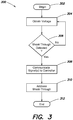
FIG. 3 illustrates aprocess 300 of mitigating or eliminating shoot-through in at least one capacitor. For example, theprocess 300 may be executed at least partially by one or more of the first shoot-throughdetector 221, the second shoot-throughdetector 223, and thecontroller 236. Theprocess 300 includes acts of obtaining a capacitor voltage value, determining if a shoot-through condition is detected, communicating control signals to a controller, and addressing the shoot-through condition. - At
act 302, theprocess 300 begins. Atact 304, a voltage value of a capacitor is obtained. For example, the first shoot-throughdetector 221 may sample a voltage level of thefirst capacitor 220 to obtain the voltage value. Atact 306, a determination is made as to whether a shoot-through condition is detected. One embodiment ofact 306 is discussed in greater detail below with respect toFIG. 4 . As shown inFIG. 4 , a shoot-through condition of a capacitor is detected where a voltage across the capacitor quickly decreases for an extended period of time. - If a shoot-through condition is not detected (306 NO), then the
process 300 returns to act 304. Otherwise, if a shoot-through condition is detected (306 YES), then theprocess 300 continues to act 308. Atact 308, responsive to determining that a shoot-through condition is detected, control signals are communicated to a controller. For example, if the first shoot-throughdetector 221 determines that thefirst capacitor 220 is experiencing a shoot-through condition, then the first shoot-throughdetector 221 may communicate a signal to thecontroller 236 indicating that thefirst capacitor 220 is experiencing a shoot-through condition. - At
act 310, a detected shoot-through condition is addressed. For example, addressing a shoot-through condition in thefirst capacitor 220 may include controlling, by thecontroller 236, thefifth switch 218 to enter an open and non-conducting position. In alternate embodiments, the first shoot-throughdetector 221 may control thefifth switch 218 directly, without interacting with thecontroller 236. As discussed above, controlling thefifth switch 218 to enter an open and non-conducting position may mitigate or eliminate shoot-through by open-circuiting thefirst capacitor 220, because thefirst capacitor 220 is coupled in series with thefifth switch 218. - Addressing the shoot-through condition at
act 310 may include additional actions. For example, thecontroller 236 may trigger an alarm indicative of the shoot-through condition. Triggering the alarm may include one or more actions which alert a human operator to the shoot-through condition. For example, triggering the alarm may include sending a notification to the human operator, illuminating a Light-Emitting Diode (LED), sounding an audible alarm, and so forth. Atact 312, theprocess 300 ends. -
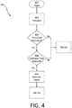
FIG. 4 illustrates aprocess 400 of detecting a shoot-through condition according to an embodiment. For example, theprocess 400 may illustrate an example ofact 306 of theprocess 300 in greater detail. Theprocess 400 may be executed by a shoot-through detector, such as the first shoot-throughdetector 221 or the second shoot-throughdetector 223. Theprocess 400 includes acts of comparing an instantaneous capacitor voltage to a previously obtained capacitor voltage, determining if a voltage threshold has been exceeded, determining if a sufficient amount of time has elapsed, and generating a detection signal. - At
act 402, theprocess 400 begins. Atact 404, an instantaneous capacitor voltage is compared to a previously-sampled capacitor voltage. For example, the previously sampled capacitor voltage may be a peak voltage acquired by a capture-and-hold circuit which has been delayed by a period of time. In some embodiments, the previously sampled peak voltage may be held and delayed for approximately 1-2 µs before being compared to an instantaneous voltage. - At
act 406, a determination is made as to whether a criterion is satisfied. For example, the first shoot-throughdetector 221 may determine if an instantaneous voltage exceeds the delayed peak voltage measurement by more than a threshold amount. The threshold amount may be expressed relative to the delayed peak voltage measurement (for example, expressed as a percentage of the delayed peak voltage measurement) or otherwise (for example, expressed as a fixed voltage value). If the criterion has not been satisfied (406 NO), then no shoot-through condition is detected (306 NO) and theprocess 400 ends by returning to 306 NO of theprocess 300. Otherwise (406 YES), theprocess 400 continues to act 408. - At
act 408, a determination is made as to whether a sufficient amount of time has elapsed. For example, the first shoot-throughdetector 221 may determine if the instantaneous voltage has continuously exceeded the delayed peak voltage measurement by more than a threshold amount for a threshold period of time. In one example, the threshold amount of time may be approximately 500 ns. If the instantaneous voltage has not continuously exceeded the delayed peak voltage measurement for a threshold amount of time (408 NO), then no shoot-through condition is detected (306 NO) and theprocess 400 ends by returning to 306 NO of theprocess 300. Otherwise (408 YES), theprocess 400 continues to act 410. Atact 410, a shoot-through detection signal is generated. For example, the first shoot-throughdetector 221 may generate a signal indicating that thefirst capacitor 220 is experiencing a shoot-through condition (306 YES). Theprocess 400 ends by returning to 306 YES of theprocess 300. -
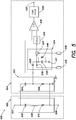
FIG. 5 illustrates a schematic diagram of a shoot-throughdetection circuit 500 according to at least one embodiment. The shoot-throughdetection circuit 500 includes acapacitor 502 and a shoot-throughdetector 504. In some embodiments, thecapacitor 502 may illustrate an embodiment of thefirst capacitor 220 or thesecond capacitor 222, and the shoot-throughdetector 504 may illustrate an embodiment of the first shoot-throughdetector 221 or the second shoot-throughdetector 223. As discussed in greater detail below, the shoot-throughdetector 504 may be configured to detect a shoot-through condition across thecapacitor 502 based at least in part on a voltage across thecapacitor 502. - The
capacitor 502 is illustrated as an equivalent circuit including anideal capacitor 506, anideal inductor 508, and anequivalent series resistor 510. As will be appreciated by one of ordinary skill in the art, theideal capacitor 506, theideal inductor 508, and theequivalent series resistor 510 are not physical, discrete components, and are illustrated as separate components for clarity of explanation only. Thecapacitor 502 further includes afirst connection 507 and asecond connection 509 configured to be coupled to one or more external components (not illustrated). - The shoot-through
detector 504 includes a blocking andsensing circuit 512, a peak detection and holdcircuit 514, adelay circuit 516, acomparator 518, alogic circuit 520, and anoutput 522. The blocking andsensing circuit 512 includes aDC blocking capacitor 524 and aresistor 526. The peak detection and holdcircuit 514 includes afirst diode 528, asecond diode 530, acapacitor 532, anadder 534, and aresistor 540, and is configured to receive afirst input signal 536 and asecond input signal 538. - The
ideal capacitor 506 is coupled to thefirst connection 507 and theDC blocking capacitor 524 at a first connection, and theideal inductor 508 at a second connection. Theideal inductor 508 is coupled to theideal capacitor 506 at a first connection, and theequivalent series resistor 510 at a second connection. Theequivalent series resistor 510 is coupled to theideal inductor 508 at a first connection, and is coupled to a reference node 511 (for example, a neutral node), thesecond connection 509, and theresistor 526 at a second connection. - The
first connection 507 is coupled to theideal capacitor 506 and theDC blocking capacitor 524 and is configured to be coupled to at least one external component. Similarly, thesecond connection 509 is coupled to theequivalent series resistor 510, thereference node 511, and theresistor 526, and is configured to be coupled to at least one external component. For example, where thecapacitor 502 illustrates an embodiment of thefirst capacitor 220, thefirst connection 507 may be configured to be coupled to thefifth switch 218, and thesecond connection 509 may be configured to be couple to thefourth switch 216, thesecond capacitor 222, and theseventh switch 226. - The
DC blocking capacitor 524 is coupled to theideal capacitor 506 and thefirst connection 507 at a first connection, and is coupled to theresistor 526, thefirst diode 528, and a non-inverting connection of thecomparator 518 at a second connection. Theresistor 526 is coupled to theDC blocking capacitor 524, thefirst diode 528, and the non-inverting connection of thecomparator 518 at a first connection, and is coupled to thesecond connection 509, theequivalent series resistor 510, and thereference node 511 at a second connection. - The
first diode 528 is coupled to theDC blocking capacitor 524, theresistor 526, and the non-inverting connection of thecomparator 518 at an anode connection, and is coupled to a cathode connection of thesecond diode 530, thecapacitor 532, theresistor 540, and a first input of theadder 534 at a cathode connection. Thesecond diode 530 is configured to receive thefirst input signal 536 at an anode connection, and is coupled to the cathode connection of thefirst diode 528, thecapacitor 532, theresistor 540, and the first input of theadder 534 at a cathode connection. Thecapacitor 532 is coupled to the cathode connection of thefirst diode 528, the cathode connection of thesecond diode 530, and the first input of theadder 534 at a first connection, is coupled to thereference node 511 at a second connection, and is coupled in parallel with theresistor 540. Theresistor 540 is coupled to the cathode connection of thefirst diode 528, the cathode connection of thesecond diode 530, and the first input of theadder 534 at a first connection, is coupled to thereference node 511 at a second connection, and is coupled in parallel with thecapacitor 532. - The
adder 534 is coupled to thefirst diode 528, thesecond diode 530, thecapacitor 532, and theresistor 540 at a first input, is configured to receive thesecond input signal 538 at a second input, and is configured to be coupled to thedelay circuit 516 at an output. Thedelay circuit 516 is coupled to theadder 534 at an input connection, and is coupled to an inverting connection of thecomparator 518 at an output connection. - The
comparator 518 is coupled to theDC blocking capacitor 524, theresistor 526, and thefirst diode 528 at the non-inverting connection, is coupled to thedelay circuit 516 at an inverting connection, and is configured to be coupled to thelogic circuit 520 at an output connection. Thelogic circuit 520 is configured to be coupled to the output of thecomparator 518 at a first connection, and is configured to be coupled to theoutput 522 at a second connection. - As discussed above, the shoot-through
detector 504 may be configured to detect a shoot-through condition of thecapacitor 502 based on a voltage across thecapacitor 502. Generally speaking, the shoot-throughdetector 504 is configured to measure a voltage across the capacitor 502 (i.e., a voltage difference between thefirst connection 507 and the second connection 509), detect a peak value of the measured voltage, and hold the peak value for a delay period. After the delay period, the shoot-throughdetector 504 may measure the voltage across thecapacitor 502 again to obtain an instantaneous voltage, and compare the instantaneous voltage to the delayed peak voltage. If the instantaneous voltage continuously exceeds the delayed peak voltage by a threshold amount for a threshold amount of time, it may be determined that a shoot-through condition is occurring, and appropriate corrective action may be taken in response thereto. - The determination of the occurrence of the shoot-through condition may be based on a condition where the voltage across the
capacitor 502 decreases rapidly during a shoot-through condition. Because the comparison is executed between twocapacitor 502 voltage samples collected within a short period of time, the determination of the occurrence of the shoot-through condition can be relatively immune to long-term changes to properties (for example, impedance properties) of thecapacitor 502. Accordingly, the shoot-throughdetector 504 may be more reliable than a shoot-through detector configured to determine whether a capacitor voltage decreases by more than a fixed value (for example, a fixed value determined at a time of manufacture of the capacitor) independent of a previous voltage measurement of the capacitor. - In one example, the shoot-through
detector 504 may receive an input voltage at the blocking andsensing circuit 512 indicative of a voltage between thefirst connection 507 and thesecond connection 509. The shoot-throughdetector 504 is configured to filter the input voltage by blocking a DC component of the input voltage (for example, using theDC blocking capacitor 524 of the blocking and sensing circuit 512), and to provide the filtered input voltage to the non-inverting connection of thecomparator 518 and the peak detection and holdcircuit 514. - The peak detection and hold
circuit 514 is configured to detect a peak of the received input voltage, hold the peak voltage for a period of time, and provide an output signal indicative of the peak voltage to thedelay circuit 516. Thedelay circuit 516 holds the output signal for a period of time (for example, 1-2 µs) and, once the period of time has elapsed, provides the output signal to the inverting connection of thecomparator 518. In some embodiments, thedelay circuit 516 may also include an analog low-pass filter which can be used to generate a signal delay. Thecomparator 518 compares an instantaneous voltage received at the non-inverting terminal with a delayed output signal received at the inverting connection, and provides an output signal indicative of the comparison. - The output signal is indicative of a relationship between the inputs received at the inverting connection and the non-inverting connection. For example, if the input received at the non-inverting terminal (i.e., the instantaneous voltage) is greater than the input received at the inverting terminal (i.e., a voltage signal derived from the delayed peak voltage), then the
comparator 518 will output a signal indicative thereof (for example, a logical HIGH or logical LOW value). Otherwise, if the input voltage received at the non-inverting terminal is less than the input voltage received at the inverting terminal, then thecomparator 518 will output a signal having an opposite value (for example, a logical LOW or logical HIGH value). - The
logic circuit 520 determines whether the output signal of thecomparator 518 has continuously indicated that the instantaneous voltage is greater than the output of thedelay circuit 516 for more than a threshold period of time (for example, 500 ns). If so, then thelogic circuit 520 may determine that a shoot-through condition is occurring and output a signal to theoutput 522 indicative of the shoot-through condition. For example, thelogic circuit 520 may communicate the signal, via theoutput 522, to a controller (for example, the controller 236) to automatically address the shoot-through condition. As discussed above, addressing the shoot-through condition may include opening a switching device coupled to the capacitor exhibiting the shoot-through condition. - The peak detection and hold
circuit 514 will now be described in greater detail. In some embodiments, the peak detection and holdcircuit 514 outputs at least a minimum base value where an input received from thecapacitor 502 is less than the minimum base value. The minimum base value is set by thefirst input signal 536 and may be implemented to avoid false positive detection of a shoot-through condition. - For purposes of explanation only, operation of the peak detection and hold
circuit 514 may be regarded as having an idle state and a normal state. Generally speaking, the states may be defined by whether thesecond diode 530 is reverse-biased (for example, in the normal state) or forward-biased (for example, in the idle state). - In the idle state, the
capacitor 532 is substantially discharged and is not being charged by thecapacitor 502. In one example, thefirst input signal 536 is configured to have a sufficiently-large value to forward-bias thesecond diode 530 at least when thecapacitor 532 is substantially discharged. In other examples, thefirst input signal 536 may be configured to forward-bias thesecond diode 530 when thecapacitor 532 is charged to various partial levels of charge. When thesecond diode 530 is forward-biased, thefirst input signal 536 is provided to the first input of theadder 534. - In the normal state, the
capacitor 532 is being charged by, or remains at least partially charged from, thecapacitor 502. As will be appreciated by one or ordinary skill in the art, thefirst diode 528 and thecapacitor 532 may act as a peak hold circuit configured to hold a peak of a voltage signal received at the anode of thefirst diode 528. Thesecond diode 530 remains in a reverse-biased state. The first input of theadder 534 receives an input signal from thecapacitor 532 indicative of a most-recently-received peak voltage value across thecapacitor 502. - The
adder 534 is configured to receive at least one of thefirst input signal 536 and the signal indicative of the most-recently-received peak voltage value across thecapacitor 502 at a first input, and thesecond input signal 538 at a second input. Theadder 534 sums the signals received at the first input and the second input, and outputs the sum to thedelay circuit 516. - The
second input signal 538 may be implemented to provide a buffer value indicative of an amount by which the instantaneous voltage must exceed the delayed peak voltage for the shoot-through condition to be detected. Stated mathematically, while the peak detection and holdcircuit 514 is in the normal state, thecomparator 518 will output a signal indicating that a shoot-through condition is detected if,
comparator 518, Vpeak is a most-recently-held peak voltage across thecapacitor 502 held by thecapacitor 532, and Vbuffer is a buffer voltage derived from thesecond input signal 538. Accordingly, thesecond input signal 538 prevents thecomparator 518 from providing a false positive output where Vinstantaneous exceeds Vpeak by a negligible amount (i.e., an amount less than Vbuffer), which may occur even where no shoot-through condition is present. - Embodiments of a shoot-through detector described herein can provide shoot-through detection with minimized cost, complexity, and physical footprint relative to the prior art. Moreover, the embodiments described herein are highly configurable. For example, the
first input signal 536 and thesecond input signal 538 may be configured to determine an appropriate balance between shoot-through detection false positives and misses. In one example, a current value corresponding to each of thefirst input signal 536 and thesecond input signal 538 is approximately 200 A. In this example, the shoot-through current must be at least 200 A larger than the largest current previously detected during normal operation for a threshold period of time to determine that a shoot-through condition is occurring. - The delay period introduced by the
delay circuit 516 may also be configurable. For example, in one embodiment, the delay period introduced by thedelay circuit 516 is within a range of 1-2 µs. Similarly, the minimum amount of time during which thecomparator 518 must output a signal indicative of the shoot-through condition may be configured via thelogic circuit 520. - Furthermore, components of the shoot-through detector 503 may be selected according to various design preferences. For example, in one embodiment, it may be preferable for the
capacitor 532 to be selected to have a fast charging time and a slow discharging time. In one example, thecapacitor 532 is a 10 nF capacitor having a charging time constant of approximately 0.2 µs and a discharging time constant of approximately 1 ms. Similarly, thecomparator 518 may be selected according to various design preferences. In some embodiments, for example, it may be desirable to select a comparator having a minimal propagation delay such that a time between shoot-through detection and shoot-through mitigation or elimination is reduced. - As discussed above, at least some of the embodiments described herein may be implemented in Uninterruptible Power Supplies (UPSs). For example,
FIG. 6 is a block diagram of aUPS 600. TheUPS 600 includes aninput 602, an AC/DC converter 604, aDC link 606, a DC/DC converter 608, abattery 610, acontroller 612, a DC/AC inverter 614, and anoutput 616. Theinput 602 is coupled to the AC/DC converter 604 and an AC power source (not pictured), such as an AC mains power supply. The AC/DC converter 604 is coupled to theinput 602 and to the DC link 606, and is communicatively coupled to thecontroller 612. - The DC link 606 is coupled to the AC/
DC converter 604, the DC/DC converter 608, and to the DC/AC inverter 614. The DC/DC converter 608 is coupled to the DC link 606 and to thebattery 610, and is communicatively coupled to thecontroller 612. Thebattery 610 is coupled to the DC/DC converter 608. The DC/AC inverter 614 is coupled to the DC link 606 and to theoutput 616, and is communicatively coupled to thecontroller 612. Theoutput 616 is coupled to the DC/AC inverter 614, and to an external load (not pictured). - The
input 602 is configured to be coupled to an AC mains power source and to receive input AC power having an input voltage level. For example, theinput 602 may be configured to receive one-phase AC mains power, three-phase AC mains power, or input power having a different number of phases. TheUPS 600 is configured to operate in different modes of operation based on the input voltage level of the AC power provided to theinput 602. When AC power provided to theinput 602 is acceptable (i.e., by having parameters that meet specified values), theUPS 600 operates in a normal mode of operation. - In the normal mode of operation, AC power received at the
input 602 is provided to the AC/DC converter 604. The AC/DC converter 604 converts the AC power into DC power and provides the DC power to theDC link 606. The DC link 606 may include one or more energy storage devices (for example, one or more capacitors) configured to store received energy. In some examples, the AC/DC converter 604 may include therectifier 200, therectifier 300, and/or therectifier 400. The DC link 606 distributes the DC power to the DC/DC converter 608 and to the DC/AC inverter 614. The DC/DC converter 608 converts the received DC power and provides the converted DC power to thebattery 610 to charge thebattery 610. The DC/AC inverter 614 receives DC power from the DC link 606, converts the DC power into regulated AC power, and provides the regulated AC power to theoutput 616 to be delivered to a load. - When AC power provided to the
input 602 from the AC mains power source is not acceptable (i.e., by having parameters that do not meet specified values), theUPS 600 operates in a backup mode of operation. In the backup mode of operation, DC power is discharged from thebattery 610 to the DC/DC converter 608. The DC/DC converter 608 converts the received DC power and provides the DC power to theDC link 606. The DC link 606 provides the received power to the DC/AC inverter 614. The DC/AC inverter 614 receives the DC power from the DC link 606, converts the DC power into regulated AC power, and provides the regulated AC power to theoutput 616. - During the backup mode of operation, power provided to the DC link 606 is provided by the
battery 610, and during the normal mode of operation, power provided to the DC link 606 is provided by a power source connected to theinput 602. Power provided to the DC link 606 is subsequently drawn by the DC/AC inverter 614 to generate AC power, and to supply the AC power to an external load connected to theoutput 616. In alternate embodiments, thebattery 610 may be replaced by an alternate energy storage device, such as a capacitor or flywheel. - In some embodiments, a shoot-through detection circuit, such as the shoot-through
detector 504, may be implemented in connection with one or more components of theUPS 600. For example, a shoot-through detector may be implemented in connection with one or more of the AC/DC converter 604, the DC link 606, or the DC/AC inverter 614. - As discussed above, the shoot-through detector may be implemented in connection with at least one controller, such as the
controller 236, thecontroller 612, or a combination thereof. Using data stored in associated memory, the controller also executes one or more instructions stored on one or more non-transitory computer-readable media that may result in manipulated data. In some examples, the controller may include one or more processors or other types of controllers. In one example, the controller is a commercially available, general purpose processor. In another example, the controller is a Field-Programmable Gate Array (FPGA) controller. - In yet another example, the controller performs a portion of the functions disclosed herein on a processor and performs another portion using an Application-Specific Integrated Circuit (ASIC) tailored to perform particular operations. As illustrated by these examples, examples in accordance with the present invention may perform the operations described herein using many specific combinations of hardware and software and the invention is not limited to any particular combination of hardware and software components.
- In some embodiments, one or more controllers may perform one or more of the operations discussed herein. For example, although the first shoot-through
detector 221, the second shoot-throughdetector 223, the shoot-throughdetector 504, thecontroller 236, and thecontroller 612 are illustrated as discrete components, in some embodiments, a single controller may be configured to execute the functionality of each of the foregoing components. For example, thecontroller 236 may be configured to execute the functionality of the shoot-throughdetectors detectors controller 236. - Having thus described several aspects of at least one embodiment, it is to be appreciated various alterations, modifications, and improvements will readily occur to those skilled in the art. Such alterations, modifications, and improvements are intended to be part of this disclosure, and are intended to be within the scope of the disclosure. Accordingly, the foregoing description and drawings are by way of example only.
Claims (15)
- An Uninterruptible Power Supply (UPS) system comprising:an input configured to receive input power;an interface configured to be coupled to a backup power supply and to receive backup power from the backup power supply;an output configured to provide output power derived from at least one of the input power and the backup power to a load;a power converter coupled to the input;at least one capacitor; anda shoot-through detector coupled to the at least one capacitor and being configured to:obtain a first voltage value indicative of a first voltage across the at least one capacitor;obtain a second voltage value indicative of a second voltage across the at least one capacitor;compare the first voltage value to the second voltage value;determine, based on the comparison, that the at least one capacitor is experiencing a shoot-through condition; andprovide an output signal indicative of the shoot-through condition.
- The UPS system of claim 1, wherein the shoot-through detector comprises a delay circuit configured to delay the first voltage value by a delay period to generate a delayed first voltage value.
- The UPS system of claim 2, wherein the shoot-through detector further comprises a comparator having:a first input configured to receive the delayed first voltage value;a second input configured to receive the second voltage value; andan output configured to output a signal indicative of a shoot-through condition responsive to determining that the second voltage value is greater than the first voltage value.
- The UPS system of claim 3, wherein the shoot-through detector further comprises a logic circuit configured to:receive, from the output of the comparator, the output signal indicative of the shoot-through condition; andoutput, responsive to receiving the output signal for at least a threshold amount of time, a shoot-through signal indicative of the shoot-through condition.
- The UPS system of claim 4, wherein the logic circuit is further configured to receive a parameter configuration value to set the threshold amount of time.
- The UPS system of claim 1, wherein the shoot-through detector further comprises a peak detection and hold circuit configured to receive the first voltage, detect a peak of the first voltage, and hold the peak of the first voltage, the peak of the first voltage corresponding to the first voltage value.
- The UPS system of claim 1, further comprising a controller coupled to the shoot-through detector,
wherein the shoot-through detector is further configured to provide the output signal to the controller, and
wherein the controller is configured to control at least one switching device coupled to the at least one capacitor to be in an open and non-conducting position in response to receiving the output signal. - A method of detecting a shoot-through condition in a capacitor, the method comprising:obtaining a first voltage value, the first voltage value being indicative of a first voltage across the capacitor;obtaining a second voltage value, the second voltage value being indicative of a second voltage across the capacitor;comparing the first voltage value to the second voltage value;determining, based on the comparison, that the capacitor is experiencing a shoot-through condition; andoutputting an output signal indicative of the shoot-through condition.
- The method of claim 8, wherein obtaining the second voltage value includes obtaining the second voltage value after a delay period from a time at which the first voltage value is obtained.
- The method of claim 8, further comprising mitigating, responsive to outputting the output signal, the shoot-through condition.
- The method of claim 10, wherein mitigating the shoot-through condition includes controlling at least one switching device coupled with the capacitor to be in an open and non-conducting state.
- The method of claim 8, wherein determining that the capacitor is experiencing a shoot-through condition includes determining that the second voltage value exceeds the first voltage value by at least a threshold amount for a threshold period of time.
- The method of claim 12, further comprising receiving, from a user, a configuration parameter corresponding to the threshold amount.
- The method of claim 12, further comprising receiving, from a user, a configuration parameter corresponding to the threshold period of time.
- The method of claim 8, wherein obtaining the first voltage value includes detecting a peak of the first voltage and holding the peak of the first voltage.
Priority Applications (1)
| Application Number | Priority Date | Filing Date | Title |
|---|---|---|---|
| EP22177372.4A EP4071952A1 (en) | 2018-11-30 | 2019-11-12 | Detection of shoot-through in power converters |
Applications Claiming Priority (1)
| Application Number | Priority Date | Filing Date | Title |
|---|---|---|---|
| US16/205,684 US11050338B2 (en) | 2018-11-30 | 2018-11-30 | Detection of shoot-through in power converters |
Related Child Applications (1)
| Application Number | Title | Priority Date | Filing Date |
|---|---|---|---|
| EP22177372.4A Division EP4071952A1 (en) | 2018-11-30 | 2019-11-12 | Detection of shoot-through in power converters |
Publications (2)
| Publication Number | Publication Date |
|---|---|
| EP3661009A1 true EP3661009A1 (en) | 2020-06-03 |
| EP3661009B1 EP3661009B1 (en) | 2022-07-06 |
Family
ID=68581315
Family Applications (2)
| Application Number | Title | Priority Date | Filing Date |
|---|---|---|---|
| EP19208691.6A Active EP3661009B1 (en) | 2018-11-30 | 2019-11-12 | Detection of shoot-through in power converters |
| EP22177372.4A Pending EP4071952A1 (en) | 2018-11-30 | 2019-11-12 | Detection of shoot-through in power converters |
Family Applications After (1)
| Application Number | Title | Priority Date | Filing Date |
|---|---|---|---|
| EP22177372.4A Pending EP4071952A1 (en) | 2018-11-30 | 2019-11-12 | Detection of shoot-through in power converters |
Country Status (3)
| Country | Link |
|---|---|
| US (1) | US11050338B2 (en) |
| EP (2) | EP3661009B1 (en) |
| CN (1) | CN111257703A (en) |
Citations (2)
| Publication number | Priority date | Publication date | Assignee | Title |
|---|---|---|---|---|
| US20130003429A1 (en) * | 2010-02-25 | 2013-01-03 | Mitsubishi Electric Corporation | Power conversion device |
| US20170149346A1 (en) * | 2014-06-27 | 2017-05-25 | Schneider Electric It Corporation | 3-level power topology |
Family Cites Families (5)
| Publication number | Priority date | Publication date | Assignee | Title |
|---|---|---|---|---|
| US8830637B2 (en) * | 2010-08-31 | 2014-09-09 | Texas Instruments Incorporated | Methods and apparatus to clamp overvoltages for alternating current systems |
| US10148188B2 (en) * | 2016-09-06 | 2018-12-04 | Fairchild Semiconductor Corporation | Clamp voltage detection and over-voltage protection for power supply topologies |
| US10164531B2 (en) * | 2017-02-15 | 2018-12-25 | Dialog Semiconductor (Uk) Limited | Adaptive control method for generating non overlapping time in output devices |
| US11152780B2 (en) * | 2017-08-31 | 2021-10-19 | Eaton Intelligent Power Limited | Adjustable speed drive with integrated solid-state circuit breaker and method of operation thereof |
| DE102018129909B4 (en) * | 2018-11-27 | 2020-12-31 | Danfoss Power Electronics A/S | Power electronics device |
-
2018
- 2018-11-30 US US16/205,684 patent/US11050338B2/en active Active
-
2019
- 2019-11-12 EP EP19208691.6A patent/EP3661009B1/en active Active
- 2019-11-12 EP EP22177372.4A patent/EP4071952A1/en active Pending
- 2019-11-29 CN CN201911203553.6A patent/CN111257703A/en active Pending
Patent Citations (2)
| Publication number | Priority date | Publication date | Assignee | Title |
|---|---|---|---|---|
| US20130003429A1 (en) * | 2010-02-25 | 2013-01-03 | Mitsubishi Electric Corporation | Power conversion device |
| US20170149346A1 (en) * | 2014-06-27 | 2017-05-25 | Schneider Electric It Corporation | 3-level power topology |
Also Published As
| Publication number | Publication date |
|---|---|
| EP4071952A1 (en) | 2022-10-12 |
| EP3661009B1 (en) | 2022-07-06 |
| CN111257703A (en) | 2020-06-09 |
| US20200177069A1 (en) | 2020-06-04 |
| US11050338B2 (en) | 2021-06-29 |
Similar Documents
| Publication | Publication Date | Title |
|---|---|---|
| US10756567B2 (en) | Uninterruptible power supply device | |
| US9154000B2 (en) | Uninterruptible power supply apparatus including a control circuit that executes a first mode when supply of a first AC electric power from a commercial AC power supply is resumed at a time of discharge end | |
| US9787193B2 (en) | Switching power supply and method for controlling voltage of bulk capacitor in the switching power supply | |
| US9705397B2 (en) | AC-DC converter with output power suppression | |
| US9024609B2 (en) | Circuit and method for providing hold-up time in a DC-DC converter | |
| CN107155383B (en) | Uninterruptible power supply device | |
| US11088528B2 (en) | Arc detection circuit, switch system, power conditioner system and arc detection method | |
| US10340730B2 (en) | Uninterruptible power supply apparatus | |
| US20210057997A1 (en) | Power supply device | |
| US9979309B1 (en) | Synchronous rectification controller | |
| US20190165604A1 (en) | Emergency dimming apparatus | |
| CN108226839B (en) | Converter, and abnormality detection method and device of Hall sensor | |
| US10069438B2 (en) | Power converter with capacitor voltage balancing | |
| JP2008228494A (en) | Inverter for coordinating system | |
| EP3661009B1 (en) | Detection of shoot-through in power converters | |
| US11271419B2 (en) | Uninterruptible power supply device | |
| JP6994673B2 (en) | Power conversion system | |
| EP3879656A1 (en) | Fault condition detection system and method | |
| US11831249B2 (en) | Power conversion apparatus | |
| US10666130B2 (en) | Electric power conversion system | |
| KR20130042196A (en) | Protection circuit for pulse power generator and protection method thereof | |
| US20230318594A1 (en) | Power Supply Device | |
| US10958158B2 (en) | Controlling discharge of x-capacitance | |
| CN219477947U (en) | Pulse stretching circuit and household appliance power module | |
| CN116365482A (en) | Overvoltage protection system |
Legal Events
| Date | Code | Title | Description |
|---|---|---|---|
| PUAI | Public reference made under article 153(3) epc to a published international application that has entered the european phase |
Free format text: ORIGINAL CODE: 0009012 |
|
| STAA | Information on the status of an ep patent application or granted ep patent |
Free format text: STATUS: THE APPLICATION HAS BEEN PUBLISHED |
|
| AK | Designated contracting states |
Kind code of ref document: A1 Designated state(s): AL AT BE BG CH CY CZ DE DK EE ES FI FR GB GR HR HU IE IS IT LI LT LU LV MC MK MT NL NO PL PT RO RS SE SI SK SM TR |
|
| AX | Request for extension of the european patent |
Extension state: BA ME |
|
| STAA | Information on the status of an ep patent application or granted ep patent |
Free format text: STATUS: REQUEST FOR EXAMINATION WAS MADE |
|
| 17P | Request for examination filed |
Effective date: 20201203 |
|
| RBV | Designated contracting states (corrected) |
Designated state(s): AL AT BE BG CH CY CZ DE DK EE ES FI FR GB GR HR HU IE IS IT LI LT LU LV MC MK MT NL NO PL PT RO RS SE SI SK SM TR |
|
| STAA | Information on the status of an ep patent application or granted ep patent |
Free format text: STATUS: EXAMINATION IS IN PROGRESS |
|
| 17Q | First examination report despatched |
Effective date: 20210803 |
|
| RIC1 | Information provided on ipc code assigned before grant |
Ipc: H02M 7/487 20070101ALI20211221BHEP Ipc: H02M 5/458 20060101ALI20211221BHEP Ipc: H02M 1/38 20070101ALI20211221BHEP Ipc: H02M 1/32 20070101ALI20211221BHEP Ipc: H02H 7/122 20060101ALI20211221BHEP Ipc: H02H 7/10 20060101ALI20211221BHEP Ipc: H02J 9/06 20060101AFI20211221BHEP |
|
| GRAP | Despatch of communication of intention to grant a patent |
Free format text: ORIGINAL CODE: EPIDOSNIGR1 |
|
| STAA | Information on the status of an ep patent application or granted ep patent |
Free format text: STATUS: GRANT OF PATENT IS INTENDED |
|
| INTG | Intention to grant announced |
Effective date: 20220214 |
|
| GRAS | Grant fee paid |
Free format text: ORIGINAL CODE: EPIDOSNIGR3 |
|
| GRAA | (expected) grant |
Free format text: ORIGINAL CODE: 0009210 |
|
| STAA | Information on the status of an ep patent application or granted ep patent |
Free format text: STATUS: THE PATENT HAS BEEN GRANTED |
|
| AK | Designated contracting states |
Kind code of ref document: B1 Designated state(s): AL AT BE BG CH CY CZ DE DK EE ES FI FR GB GR HR HU IE IS IT LI LT LU LV MC MK MT NL NO PL PT RO RS SE SI SK SM TR |
|
| RAP3 | Party data changed (applicant data changed or rights of an application transferred) |
Owner name: SCHNEIDER ELECTRIC IT CORPORATION |
|
| REG | Reference to a national code |
Ref country code: AT Ref legal event code: REF Ref document number: 1503579 Country of ref document: AT Kind code of ref document: T Effective date: 20220715 Ref country code: CH Ref legal event code: EP |
|
| REG | Reference to a national code |
Ref country code: DE Ref legal event code: R096 Ref document number: 602019016647 Country of ref document: DE |
|
| REG | Reference to a national code |
Ref country code: IE Ref legal event code: FG4D |
|
| REG | Reference to a national code |
Ref country code: LT Ref legal event code: MG9D |
|
| REG | Reference to a national code |
Ref country code: NL Ref legal event code: MP Effective date: 20220706 |
|
| PG25 | Lapsed in a contracting state [announced via postgrant information from national office to epo] |
Ref country code: SE Free format text: LAPSE BECAUSE OF FAILURE TO SUBMIT A TRANSLATION OF THE DESCRIPTION OR TO PAY THE FEE WITHIN THE PRESCRIBED TIME-LIMIT Effective date: 20220706 Ref country code: RS Free format text: LAPSE BECAUSE OF FAILURE TO SUBMIT A TRANSLATION OF THE DESCRIPTION OR TO PAY THE FEE WITHIN THE PRESCRIBED TIME-LIMIT Effective date: 20220706 Ref country code: PT Free format text: LAPSE BECAUSE OF FAILURE TO SUBMIT A TRANSLATION OF THE DESCRIPTION OR TO PAY THE FEE WITHIN THE PRESCRIBED TIME-LIMIT Effective date: 20221107 Ref country code: NO Free format text: LAPSE BECAUSE OF FAILURE TO SUBMIT A TRANSLATION OF THE DESCRIPTION OR TO PAY THE FEE WITHIN THE PRESCRIBED TIME-LIMIT Effective date: 20221006 Ref country code: NL Free format text: LAPSE BECAUSE OF FAILURE TO SUBMIT A TRANSLATION OF THE DESCRIPTION OR TO PAY THE FEE WITHIN THE PRESCRIBED TIME-LIMIT Effective date: 20220706 Ref country code: LV Free format text: LAPSE BECAUSE OF FAILURE TO SUBMIT A TRANSLATION OF THE DESCRIPTION OR TO PAY THE FEE WITHIN THE PRESCRIBED TIME-LIMIT Effective date: 20220706 Ref country code: LT Free format text: LAPSE BECAUSE OF FAILURE TO SUBMIT A TRANSLATION OF THE DESCRIPTION OR TO PAY THE FEE WITHIN THE PRESCRIBED TIME-LIMIT Effective date: 20220706 Ref country code: FI Free format text: LAPSE BECAUSE OF FAILURE TO SUBMIT A TRANSLATION OF THE DESCRIPTION OR TO PAY THE FEE WITHIN THE PRESCRIBED TIME-LIMIT Effective date: 20220706 Ref country code: ES Free format text: LAPSE BECAUSE OF FAILURE TO SUBMIT A TRANSLATION OF THE DESCRIPTION OR TO PAY THE FEE WITHIN THE PRESCRIBED TIME-LIMIT Effective date: 20220706 |
|
| REG | Reference to a national code |
Ref country code: AT Ref legal event code: MK05 Ref document number: 1503579 Country of ref document: AT Kind code of ref document: T Effective date: 20220706 |
|
| PG25 | Lapsed in a contracting state [announced via postgrant information from national office to epo] |
Ref country code: PL Free format text: LAPSE BECAUSE OF FAILURE TO SUBMIT A TRANSLATION OF THE DESCRIPTION OR TO PAY THE FEE WITHIN THE PRESCRIBED TIME-LIMIT Effective date: 20220706 Ref country code: IS Free format text: LAPSE BECAUSE OF FAILURE TO SUBMIT A TRANSLATION OF THE DESCRIPTION OR TO PAY THE FEE WITHIN THE PRESCRIBED TIME-LIMIT Effective date: 20221106 Ref country code: HR Free format text: LAPSE BECAUSE OF FAILURE TO SUBMIT A TRANSLATION OF THE DESCRIPTION OR TO PAY THE FEE WITHIN THE PRESCRIBED TIME-LIMIT Effective date: 20220706 Ref country code: GR Free format text: LAPSE BECAUSE OF FAILURE TO SUBMIT A TRANSLATION OF THE DESCRIPTION OR TO PAY THE FEE WITHIN THE PRESCRIBED TIME-LIMIT Effective date: 20221007 |
|
| REG | Reference to a national code |
Ref country code: DE Ref legal event code: R097 Ref document number: 602019016647 Country of ref document: DE |
|
| PG25 | Lapsed in a contracting state [announced via postgrant information from national office to epo] |
Ref country code: SM Free format text: LAPSE BECAUSE OF FAILURE TO SUBMIT A TRANSLATION OF THE DESCRIPTION OR TO PAY THE FEE WITHIN THE PRESCRIBED TIME-LIMIT Effective date: 20220706 Ref country code: RO Free format text: LAPSE BECAUSE OF FAILURE TO SUBMIT A TRANSLATION OF THE DESCRIPTION OR TO PAY THE FEE WITHIN THE PRESCRIBED TIME-LIMIT Effective date: 20220706 Ref country code: DK Free format text: LAPSE BECAUSE OF FAILURE TO SUBMIT A TRANSLATION OF THE DESCRIPTION OR TO PAY THE FEE WITHIN THE PRESCRIBED TIME-LIMIT Effective date: 20220706 Ref country code: CZ Free format text: LAPSE BECAUSE OF FAILURE TO SUBMIT A TRANSLATION OF THE DESCRIPTION OR TO PAY THE FEE WITHIN THE PRESCRIBED TIME-LIMIT Effective date: 20220706 Ref country code: AT Free format text: LAPSE BECAUSE OF FAILURE TO SUBMIT A TRANSLATION OF THE DESCRIPTION OR TO PAY THE FEE WITHIN THE PRESCRIBED TIME-LIMIT Effective date: 20220706 |
|
| PLBE | No opposition filed within time limit |
Free format text: ORIGINAL CODE: 0009261 |
|
| STAA | Information on the status of an ep patent application or granted ep patent |
Free format text: STATUS: NO OPPOSITION FILED WITHIN TIME LIMIT |
|
| PG25 | Lapsed in a contracting state [announced via postgrant information from national office to epo] |
Ref country code: SK Free format text: LAPSE BECAUSE OF FAILURE TO SUBMIT A TRANSLATION OF THE DESCRIPTION OR TO PAY THE FEE WITHIN THE PRESCRIBED TIME-LIMIT Effective date: 20220706 Ref country code: EE Free format text: LAPSE BECAUSE OF FAILURE TO SUBMIT A TRANSLATION OF THE DESCRIPTION OR TO PAY THE FEE WITHIN THE PRESCRIBED TIME-LIMIT Effective date: 20220706 |
|
| 26N | No opposition filed |
Effective date: 20230411 |
|
| PG25 | Lapsed in a contracting state [announced via postgrant information from national office to epo] |
Ref country code: MC Free format text: LAPSE BECAUSE OF FAILURE TO SUBMIT A TRANSLATION OF THE DESCRIPTION OR TO PAY THE FEE WITHIN THE PRESCRIBED TIME-LIMIT Effective date: 20220706 Ref country code: AL Free format text: LAPSE BECAUSE OF FAILURE TO SUBMIT A TRANSLATION OF THE DESCRIPTION OR TO PAY THE FEE WITHIN THE PRESCRIBED TIME-LIMIT Effective date: 20220706 |
|
| REG | Reference to a national code |
Ref country code: CH Ref legal event code: PL |
|
| REG | Reference to a national code |
Ref country code: BE Ref legal event code: MM Effective date: 20221130 |
|
| PG25 | Lapsed in a contracting state [announced via postgrant information from national office to epo] |
Ref country code: LI Free format text: LAPSE BECAUSE OF NON-PAYMENT OF DUE FEES Effective date: 20221130 Ref country code: CH Free format text: LAPSE BECAUSE OF NON-PAYMENT OF DUE FEES Effective date: 20221130 |
|
| PG25 | Lapsed in a contracting state [announced via postgrant information from national office to epo] |
Ref country code: SI Free format text: LAPSE BECAUSE OF FAILURE TO SUBMIT A TRANSLATION OF THE DESCRIPTION OR TO PAY THE FEE WITHIN THE PRESCRIBED TIME-LIMIT Effective date: 20220706 Ref country code: LU Free format text: LAPSE BECAUSE OF NON-PAYMENT OF DUE FEES Effective date: 20221112 |
|
| PG25 | Lapsed in a contracting state [announced via postgrant information from national office to epo] |
Ref country code: IE Free format text: LAPSE BECAUSE OF NON-PAYMENT OF DUE FEES Effective date: 20221112 |
|
| PG25 | Lapsed in a contracting state [announced via postgrant information from national office to epo] |
Ref country code: BE Free format text: LAPSE BECAUSE OF NON-PAYMENT OF DUE FEES Effective date: 20221130 |
|
| PGFP | Annual fee paid to national office [announced via postgrant information from national office to epo] |
Ref country code: GB Payment date: 20231121 Year of fee payment: 5 |
|
| PG25 | Lapsed in a contracting state [announced via postgrant information from national office to epo] |
Ref country code: IT Free format text: LAPSE BECAUSE OF FAILURE TO SUBMIT A TRANSLATION OF THE DESCRIPTION OR TO PAY THE FEE WITHIN THE PRESCRIBED TIME-LIMIT Effective date: 20220706 |
|
| PGFP | Annual fee paid to national office [announced via postgrant information from national office to epo] |
Ref country code: FR Payment date: 20231123 Year of fee payment: 5 Ref country code: DE Payment date: 20231127 Year of fee payment: 5 |
|
| PG25 | Lapsed in a contracting state [announced via postgrant information from national office to epo] |
Ref country code: HU Free format text: LAPSE BECAUSE OF FAILURE TO SUBMIT A TRANSLATION OF THE DESCRIPTION OR TO PAY THE FEE WITHIN THE PRESCRIBED TIME-LIMIT; INVALID AB INITIO Effective date: 20191112 |
|
| PG25 | Lapsed in a contracting state [announced via postgrant information from national office to epo] |
Ref country code: CY Free format text: LAPSE BECAUSE OF FAILURE TO SUBMIT A TRANSLATION OF THE DESCRIPTION OR TO PAY THE FEE WITHIN THE PRESCRIBED TIME-LIMIT Effective date: 20220706 |