EP3660497A1 - Nanoparticle-based semiconductor structural element comprising a pn-junction - Google Patents
Nanoparticle-based semiconductor structural element comprising a pn-junction Download PDFInfo
- Publication number
- EP3660497A1 EP3660497A1 EP18208574.6A EP18208574A EP3660497A1 EP 3660497 A1 EP3660497 A1 EP 3660497A1 EP 18208574 A EP18208574 A EP 18208574A EP 3660497 A1 EP3660497 A1 EP 3660497A1
- Authority
- EP
- European Patent Office
- Prior art keywords
- nanoparticle
- nanoparticles
- based semiconductor
- sub
- structural element
- Prior art date
- Legal status (The legal status is an assumption and is not a legal conclusion. Google has not performed a legal analysis and makes no representation as to the accuracy of the status listed.)
- Withdrawn
Links
- 239000002105 nanoparticle Substances 0.000 title claims abstract description 397
- 239000004065 semiconductor Substances 0.000 title claims abstract description 126
- 239000000463 material Substances 0.000 claims description 67
- 150000001875 compounds Chemical class 0.000 claims description 21
- 125000003636 chemical group Chemical group 0.000 claims description 17
- 150000004770 chalcogenides Chemical class 0.000 claims description 14
- 230000008859 change Effects 0.000 claims description 13
- 229910052723 transition metal Inorganic materials 0.000 claims description 13
- 150000003624 transition metals Chemical class 0.000 claims description 13
- 239000012491 analyte Substances 0.000 claims description 12
- 230000003321 amplification Effects 0.000 claims description 11
- 238000003199 nucleic acid amplification method Methods 0.000 claims description 11
- 229910052798 chalcogen Inorganic materials 0.000 claims description 10
- 150000001787 chalcogens Chemical class 0.000 claims description 10
- 229910052760 oxygen Inorganic materials 0.000 claims description 10
- QVGXLLKOCUKJST-UHFFFAOYSA-N atomic oxygen Chemical compound [O] QVGXLLKOCUKJST-UHFFFAOYSA-N 0.000 claims description 9
- 238000011156 evaluation Methods 0.000 claims description 9
- 239000001301 oxygen Substances 0.000 claims description 9
- 229910052717 sulfur Inorganic materials 0.000 claims description 9
- NINIDFKCEFEMDL-UHFFFAOYSA-N Sulfur Chemical compound [S] NINIDFKCEFEMDL-UHFFFAOYSA-N 0.000 claims description 8
- 239000011593 sulfur Substances 0.000 claims description 8
- 239000010410 layer Substances 0.000 description 59
- 229910010413 TiO 2 Inorganic materials 0.000 description 17
- -1 chalcogenide compound Chemical class 0.000 description 14
- XEEYBQQBJWHFJM-UHFFFAOYSA-N iron Substances [Fe] XEEYBQQBJWHFJM-UHFFFAOYSA-N 0.000 description 10
- 239000000126 substance Substances 0.000 description 10
- 239000000758 substrate Substances 0.000 description 10
- 239000012799 electrically-conductive coating Substances 0.000 description 9
- 239000011669 selenium Substances 0.000 description 9
- 230000007704 transition Effects 0.000 description 9
- 238000000576 coating method Methods 0.000 description 7
- 238000009792 diffusion process Methods 0.000 description 7
- 229910052711 selenium Inorganic materials 0.000 description 7
- 229910052714 tellurium Inorganic materials 0.000 description 7
- BUGBHKTXTAQXES-UHFFFAOYSA-N Selenium Chemical compound [Se] BUGBHKTXTAQXES-UHFFFAOYSA-N 0.000 description 6
- 239000002800 charge carrier Substances 0.000 description 6
- 239000011248 coating agent Substances 0.000 description 6
- 238000005516 engineering process Methods 0.000 description 6
- 238000004519 manufacturing process Methods 0.000 description 6
- 230000003647 oxidation Effects 0.000 description 6
- 238000007254 oxidation reaction Methods 0.000 description 6
- PORWMNRCUJJQNO-UHFFFAOYSA-N tellurium atom Chemical compound [Te] PORWMNRCUJJQNO-UHFFFAOYSA-N 0.000 description 6
- XUIMIQQOPSSXEZ-UHFFFAOYSA-N Silicon Chemical compound [Si] XUIMIQQOPSSXEZ-UHFFFAOYSA-N 0.000 description 5
- 229910052732 germanium Inorganic materials 0.000 description 5
- GNPVGFCGXDBREM-UHFFFAOYSA-N germanium atom Chemical compound [Ge] GNPVGFCGXDBREM-UHFFFAOYSA-N 0.000 description 5
- 229910052751 metal Inorganic materials 0.000 description 5
- 239000002184 metal Substances 0.000 description 5
- 229910052710 silicon Inorganic materials 0.000 description 5
- GWEVSGVZZGPLCZ-UHFFFAOYSA-N Titan oxide Chemical compound O=[Ti]=O GWEVSGVZZGPLCZ-UHFFFAOYSA-N 0.000 description 4
- 230000008901 benefit Effects 0.000 description 4
- 239000000470 constituent Substances 0.000 description 4
- 238000000034 method Methods 0.000 description 4
- 230000008569 process Effects 0.000 description 4
- 238000012545 processing Methods 0.000 description 4
- 230000035945 sensitivity Effects 0.000 description 4
- 239000010703 silicon Substances 0.000 description 4
- CURLTUGMZLYLDI-UHFFFAOYSA-N Carbon dioxide Chemical compound O=C=O CURLTUGMZLYLDI-UHFFFAOYSA-N 0.000 description 3
- 238000010276 construction Methods 0.000 description 3
- 230000000694 effects Effects 0.000 description 3
- 230000005274 electronic transitions Effects 0.000 description 3
- 150000002739 metals Chemical class 0.000 description 3
- VNWKTOKETHGBQD-UHFFFAOYSA-N methane Chemical compound C VNWKTOKETHGBQD-UHFFFAOYSA-N 0.000 description 3
- 239000000203 mixture Substances 0.000 description 3
- 229910052961 molybdenite Inorganic materials 0.000 description 3
- CWQXQMHSOZUFJS-UHFFFAOYSA-N molybdenum disulfide Chemical compound S=[Mo]=S CWQXQMHSOZUFJS-UHFFFAOYSA-N 0.000 description 3
- 229910052982 molybdenum disulfide Inorganic materials 0.000 description 3
- 231100000331 toxic Toxicity 0.000 description 3
- 230000002588 toxic effect Effects 0.000 description 3
- ITRNXVSDJBHYNJ-UHFFFAOYSA-N tungsten disulfide Chemical compound S=[W]=S ITRNXVSDJBHYNJ-UHFFFAOYSA-N 0.000 description 3
- ZOXJGFHDIHLPTG-UHFFFAOYSA-N Boron Chemical compound [B] ZOXJGFHDIHLPTG-UHFFFAOYSA-N 0.000 description 2
- OKTJSMMVPCPJKN-UHFFFAOYSA-N Carbon Chemical compound [C] OKTJSMMVPCPJKN-UHFFFAOYSA-N 0.000 description 2
- WSFSSNUMVMOOMR-UHFFFAOYSA-N Formaldehyde Chemical compound O=C WSFSSNUMVMOOMR-UHFFFAOYSA-N 0.000 description 2
- NHNBFGGVMKEFGY-UHFFFAOYSA-N Nitrate Chemical compound [O-][N+]([O-])=O NHNBFGGVMKEFGY-UHFFFAOYSA-N 0.000 description 2
- 229910019142 PO4 Inorganic materials 0.000 description 2
- 229910052796 boron Inorganic materials 0.000 description 2
- 229910052799 carbon Inorganic materials 0.000 description 2
- 229910002092 carbon dioxide Inorganic materials 0.000 description 2
- 238000013461 design Methods 0.000 description 2
- 150000002222 fluorine compounds Chemical class 0.000 description 2
- AMGQUBHHOARCQH-UHFFFAOYSA-N indium;oxotin Chemical compound [In].[Sn]=O AMGQUBHHOARCQH-UHFFFAOYSA-N 0.000 description 2
- JEIPFZHSYJVQDO-UHFFFAOYSA-N iron(III) oxide Inorganic materials O=[Fe]O[Fe]=O JEIPFZHSYJVQDO-UHFFFAOYSA-N 0.000 description 2
- 239000002082 metal nanoparticle Substances 0.000 description 2
- JKQOBWVOAYFWKG-UHFFFAOYSA-N molybdenum trioxide Chemical compound O=[Mo](=O)=O JKQOBWVOAYFWKG-UHFFFAOYSA-N 0.000 description 2
- 239000002071 nanotube Substances 0.000 description 2
- 210000002569 neuron Anatomy 0.000 description 2
- 230000007935 neutral effect Effects 0.000 description 2
- 230000001590 oxidative effect Effects 0.000 description 2
- 239000002245 particle Substances 0.000 description 2
- 235000021317 phosphate Nutrition 0.000 description 2
- 229910052699 polonium Inorganic materials 0.000 description 2
- HZEBHPIOVYHPMT-UHFFFAOYSA-N polonium atom Chemical compound [Po] HZEBHPIOVYHPMT-UHFFFAOYSA-N 0.000 description 2
- 229920000642 polymer Polymers 0.000 description 2
- NIFIFKQPDTWWGU-UHFFFAOYSA-N pyrite Chemical compound [Fe+2].[S-][S-] NIFIFKQPDTWWGU-UHFFFAOYSA-N 0.000 description 2
- 229910052683 pyrite Inorganic materials 0.000 description 2
- 239000002356 single layer Substances 0.000 description 2
- XOLBLPGZBRYERU-UHFFFAOYSA-N tin dioxide Chemical compound O=[Sn]=O XOLBLPGZBRYERU-UHFFFAOYSA-N 0.000 description 2
- 229910001887 tin oxide Inorganic materials 0.000 description 2
- XLYOFNOQVPJJNP-UHFFFAOYSA-N water Chemical compound O XLYOFNOQVPJJNP-UHFFFAOYSA-N 0.000 description 2
- QGZKDVFQNNGYKY-UHFFFAOYSA-N Ammonia Chemical compound N QGZKDVFQNNGYKY-UHFFFAOYSA-N 0.000 description 1
- RWSOTUBLDIXVET-UHFFFAOYSA-N Dihydrogen sulfide Chemical compound S RWSOTUBLDIXVET-UHFFFAOYSA-N 0.000 description 1
- GYHNNYVSQQEPJS-UHFFFAOYSA-N Gallium Chemical compound [Ga] GYHNNYVSQQEPJS-UHFFFAOYSA-N 0.000 description 1
- DGAQECJNVWCQMB-PUAWFVPOSA-M Ilexoside XXIX Chemical compound C[C@@H]1CC[C@@]2(CC[C@@]3(C(=CC[C@H]4[C@]3(CC[C@@H]5[C@@]4(CC[C@@H](C5(C)C)OS(=O)(=O)[O-])C)C)[C@@H]2[C@]1(C)O)C)C(=O)O[C@H]6[C@@H]([C@H]([C@@H]([C@H](O6)CO)O)O)O.[Na+] DGAQECJNVWCQMB-PUAWFVPOSA-M 0.000 description 1
- 229910002651 NO3 Inorganic materials 0.000 description 1
- ISWSIDIOOBJBQZ-UHFFFAOYSA-N Phenol Chemical compound OC1=CC=CC=C1 ISWSIDIOOBJBQZ-UHFFFAOYSA-N 0.000 description 1
- OAICVXFJPJFONN-UHFFFAOYSA-N Phosphorus Chemical compound [P] OAICVXFJPJFONN-UHFFFAOYSA-N 0.000 description 1
- UCKMPCXJQFINFW-UHFFFAOYSA-N Sulphide Chemical compound [S-2] UCKMPCXJQFINFW-UHFFFAOYSA-N 0.000 description 1
- RTAQQCXQSZGOHL-UHFFFAOYSA-N Titanium Chemical compound [Ti] RTAQQCXQSZGOHL-UHFFFAOYSA-N 0.000 description 1
- XLOMVQKBTHCTTD-UHFFFAOYSA-N Zinc monoxide Chemical compound [Zn]=O XLOMVQKBTHCTTD-UHFFFAOYSA-N 0.000 description 1
- YUWBVKYVJWNVLE-UHFFFAOYSA-N [N].[P] Chemical group [N].[P] YUWBVKYVJWNVLE-UHFFFAOYSA-N 0.000 description 1
- 230000001133 acceleration Effects 0.000 description 1
- 230000006978 adaptation Effects 0.000 description 1
- 229910052782 aluminium Inorganic materials 0.000 description 1
- XAGFODPZIPBFFR-UHFFFAOYSA-N aluminium Chemical compound [Al] XAGFODPZIPBFFR-UHFFFAOYSA-N 0.000 description 1
- 150000001450 anions Chemical class 0.000 description 1
- 229910052787 antimony Inorganic materials 0.000 description 1
- WATWJIUSRGPENY-UHFFFAOYSA-N antimony atom Chemical compound [Sb] WATWJIUSRGPENY-UHFFFAOYSA-N 0.000 description 1
- 229910052785 arsenic Inorganic materials 0.000 description 1
- RQNWIZPPADIBDY-UHFFFAOYSA-N arsenic atom Chemical compound [As] RQNWIZPPADIBDY-UHFFFAOYSA-N 0.000 description 1
- NFMAZVUSKIJEIH-UHFFFAOYSA-N bis(sulfanylidene)iron Chemical compound S=[Fe]=S NFMAZVUSKIJEIH-UHFFFAOYSA-N 0.000 description 1
- 239000001569 carbon dioxide Substances 0.000 description 1
- 150000001768 cations Chemical class 0.000 description 1
- 229910052729 chemical element Inorganic materials 0.000 description 1
- 238000011109 contamination Methods 0.000 description 1
- 238000007796 conventional method Methods 0.000 description 1
- 230000001419 dependent effect Effects 0.000 description 1
- 230000023077 detection of light stimulus Effects 0.000 description 1
- 238000010586 diagram Methods 0.000 description 1
- 239000002019 doping agent Substances 0.000 description 1
- 238000003487 electrochemical reaction Methods 0.000 description 1
- 229910052733 gallium Inorganic materials 0.000 description 1
- 239000007789 gas Substances 0.000 description 1
- 239000011521 glass Substances 0.000 description 1
- 229910021476 group 6 element Inorganic materials 0.000 description 1
- 239000012535 impurity Substances 0.000 description 1
- 229910052738 indium Inorganic materials 0.000 description 1
- APFVFJFRJDLVQX-UHFFFAOYSA-N indium atom Chemical compound [In] APFVFJFRJDLVQX-UHFFFAOYSA-N 0.000 description 1
- 229910000339 iron disulfide Inorganic materials 0.000 description 1
- 238000011031 large-scale manufacturing process Methods 0.000 description 1
- 238000001459 lithography Methods 0.000 description 1
- 229910052960 marcasite Inorganic materials 0.000 description 1
- WSFSSNUMVMOOMR-NJFSPNSNSA-N methanone Chemical compound O=[14CH2] WSFSSNUMVMOOMR-NJFSPNSNSA-N 0.000 description 1
- 238000012986 modification Methods 0.000 description 1
- 230000004048 modification Effects 0.000 description 1
- 150000002989 phenols Chemical class 0.000 description 1
- NBIIXXVUZAFLBC-UHFFFAOYSA-K phosphate Chemical compound [O-]P([O-])([O-])=O NBIIXXVUZAFLBC-UHFFFAOYSA-K 0.000 description 1
- 239000010452 phosphate Substances 0.000 description 1
- 150000003013 phosphoric acid derivatives Chemical class 0.000 description 1
- 229910052698 phosphorus Inorganic materials 0.000 description 1
- 239000011574 phosphorus Substances 0.000 description 1
- 239000011028 pyrite Substances 0.000 description 1
- 239000010453 quartz Substances 0.000 description 1
- 239000000376 reactant Substances 0.000 description 1
- 150000004771 selenides Chemical class 0.000 description 1
- 238000011896 sensitive detection Methods 0.000 description 1
- VYPSYNLAJGMNEJ-UHFFFAOYSA-N silicon dioxide Inorganic materials O=[Si]=O VYPSYNLAJGMNEJ-UHFFFAOYSA-N 0.000 description 1
- 238000004088 simulation Methods 0.000 description 1
- 229910052708 sodium Inorganic materials 0.000 description 1
- 239000011734 sodium Substances 0.000 description 1
- 239000007787 solid Substances 0.000 description 1
- 238000013517 stratification Methods 0.000 description 1
- 150000004763 sulfides Chemical class 0.000 description 1
- 150000004772 tellurides Chemical class 0.000 description 1
- 239000010936 titanium Substances 0.000 description 1
- 229910052719 titanium Inorganic materials 0.000 description 1
- OGIDPMRJRNCKJF-UHFFFAOYSA-N titanium oxide Inorganic materials [Ti]=O OGIDPMRJRNCKJF-UHFFFAOYSA-N 0.000 description 1
- ZNOKGRXACCSDPY-UHFFFAOYSA-N tungsten(VI) oxide Inorganic materials O=[W](=O)=O ZNOKGRXACCSDPY-UHFFFAOYSA-N 0.000 description 1
Images


Classifications
-
- G—PHYSICS
- G01—MEASURING; TESTING
- G01N—INVESTIGATING OR ANALYSING MATERIALS BY DETERMINING THEIR CHEMICAL OR PHYSICAL PROPERTIES
- G01N27/00—Investigating or analysing materials by the use of electric, electrochemical, or magnetic means
- G01N27/02—Investigating or analysing materials by the use of electric, electrochemical, or magnetic means by investigating impedance
- G01N27/04—Investigating or analysing materials by the use of electric, electrochemical, or magnetic means by investigating impedance by investigating resistance
- G01N27/12—Investigating or analysing materials by the use of electric, electrochemical, or magnetic means by investigating impedance by investigating resistance of a solid body in dependence upon absorption of a fluid; of a solid body in dependence upon reaction with a fluid, for detecting components in the fluid
- G01N27/125—Composition of the body, e.g. the composition of its sensitive layer
- G01N27/127—Composition of the body, e.g. the composition of its sensitive layer comprising nanoparticles
-
- B—PERFORMING OPERATIONS; TRANSPORTING
- B82—NANOTECHNOLOGY
- B82Y—SPECIFIC USES OR APPLICATIONS OF NANOSTRUCTURES; MEASUREMENT OR ANALYSIS OF NANOSTRUCTURES; MANUFACTURE OR TREATMENT OF NANOSTRUCTURES
- B82Y10/00—Nanotechnology for information processing, storage or transmission, e.g. quantum computing or single electron logic
-
- G—PHYSICS
- G01—MEASURING; TESTING
- G01N—INVESTIGATING OR ANALYSING MATERIALS BY DETERMINING THEIR CHEMICAL OR PHYSICAL PROPERTIES
- G01N27/00—Investigating or analysing materials by the use of electric, electrochemical, or magnetic means
- G01N27/02—Investigating or analysing materials by the use of electric, electrochemical, or magnetic means by investigating impedance
- G01N27/04—Investigating or analysing materials by the use of electric, electrochemical, or magnetic means by investigating impedance by investigating resistance
- G01N27/12—Investigating or analysing materials by the use of electric, electrochemical, or magnetic means by investigating impedance by investigating resistance of a solid body in dependence upon absorption of a fluid; of a solid body in dependence upon reaction with a fluid, for detecting components in the fluid
- G01N27/129—Diode type sensors, e.g. gas sensitive Schottky diodes
-
- H—ELECTRICITY
- H01—ELECTRIC ELEMENTS
- H01L—SEMICONDUCTOR DEVICES NOT COVERED BY CLASS H10
- H01L29/00—Semiconductor devices specially adapted for rectifying, amplifying, oscillating or switching and having potential barriers; Capacitors or resistors having potential barriers, e.g. a PN-junction depletion layer or carrier concentration layer; Details of semiconductor bodies or of electrodes thereof ; Multistep manufacturing processes therefor
- H01L29/02—Semiconductor bodies ; Multistep manufacturing processes therefor
- H01L29/06—Semiconductor bodies ; Multistep manufacturing processes therefor characterised by their shape; characterised by the shapes, relative sizes, or dispositions of the semiconductor regions ; characterised by the concentration or distribution of impurities within semiconductor regions
- H01L29/0657—Semiconductor bodies ; Multistep manufacturing processes therefor characterised by their shape; characterised by the shapes, relative sizes, or dispositions of the semiconductor regions ; characterised by the concentration or distribution of impurities within semiconductor regions characterised by the shape of the body
- H01L29/0665—Semiconductor bodies ; Multistep manufacturing processes therefor characterised by their shape; characterised by the shapes, relative sizes, or dispositions of the semiconductor regions ; characterised by the concentration or distribution of impurities within semiconductor regions characterised by the shape of the body the shape of the body defining a nanostructure
- H01L29/0669—Nanowires or nanotubes
-
- H—ELECTRICITY
- H01—ELECTRIC ELEMENTS
- H01L—SEMICONDUCTOR DEVICES NOT COVERED BY CLASS H10
- H01L29/00—Semiconductor devices specially adapted for rectifying, amplifying, oscillating or switching and having potential barriers; Capacitors or resistors having potential barriers, e.g. a PN-junction depletion layer or carrier concentration layer; Details of semiconductor bodies or of electrodes thereof ; Multistep manufacturing processes therefor
- H01L29/02—Semiconductor bodies ; Multistep manufacturing processes therefor
- H01L29/12—Semiconductor bodies ; Multistep manufacturing processes therefor characterised by the materials of which they are formed
- H01L29/24—Semiconductor bodies ; Multistep manufacturing processes therefor characterised by the materials of which they are formed including, apart from doping materials or other impurities, only semiconductor materials not provided for in groups H01L29/16, H01L29/18, H01L29/20, H01L29/22
-
- H—ELECTRICITY
- H01—ELECTRIC ELEMENTS
- H01L—SEMICONDUCTOR DEVICES NOT COVERED BY CLASS H10
- H01L29/00—Semiconductor devices specially adapted for rectifying, amplifying, oscillating or switching and having potential barriers; Capacitors or resistors having potential barriers, e.g. a PN-junction depletion layer or carrier concentration layer; Details of semiconductor bodies or of electrodes thereof ; Multistep manufacturing processes therefor
- H01L29/66—Types of semiconductor device ; Multistep manufacturing processes therefor
- H01L29/66007—Multistep manufacturing processes
- H01L29/66969—Multistep manufacturing processes of devices having semiconductor bodies not comprising group 14 or group 13/15 materials
-
- H—ELECTRICITY
- H01—ELECTRIC ELEMENTS
- H01L—SEMICONDUCTOR DEVICES NOT COVERED BY CLASS H10
- H01L29/00—Semiconductor devices specially adapted for rectifying, amplifying, oscillating or switching and having potential barriers; Capacitors or resistors having potential barriers, e.g. a PN-junction depletion layer or carrier concentration layer; Details of semiconductor bodies or of electrodes thereof ; Multistep manufacturing processes therefor
- H01L29/66—Types of semiconductor device ; Multistep manufacturing processes therefor
- H01L29/68—Types of semiconductor device ; Multistep manufacturing processes therefor controllable by only the electric current supplied, or only the electric potential applied, to an electrode which does not carry the current to be rectified, amplified or switched
- H01L29/70—Bipolar devices
- H01L29/72—Transistor-type devices, i.e. able to continuously respond to applied control signals
- H01L29/73—Bipolar junction transistors
- H01L29/737—Hetero-junction transistors
- H01L29/7371—Vertical transistors
-
- H—ELECTRICITY
- H01—ELECTRIC ELEMENTS
- H01L—SEMICONDUCTOR DEVICES NOT COVERED BY CLASS H10
- H01L29/00—Semiconductor devices specially adapted for rectifying, amplifying, oscillating or switching and having potential barriers; Capacitors or resistors having potential barriers, e.g. a PN-junction depletion layer or carrier concentration layer; Details of semiconductor bodies or of electrodes thereof ; Multistep manufacturing processes therefor
- H01L29/66—Types of semiconductor device ; Multistep manufacturing processes therefor
- H01L29/86—Types of semiconductor device ; Multistep manufacturing processes therefor controllable only by variation of the electric current supplied, or only the electric potential applied, to one or more of the electrodes carrying the current to be rectified, amplified, oscillated or switched
- H01L29/861—Diodes
-
- B—PERFORMING OPERATIONS; TRANSPORTING
- B82—NANOTECHNOLOGY
- B82Y—SPECIFIC USES OR APPLICATIONS OF NANOSTRUCTURES; MEASUREMENT OR ANALYSIS OF NANOSTRUCTURES; MANUFACTURE OR TREATMENT OF NANOSTRUCTURES
- B82Y15/00—Nanotechnology for interacting, sensing or actuating, e.g. quantum dots as markers in protein assays or molecular motors
-
- G—PHYSICS
- G01—MEASURING; TESTING
- G01N—INVESTIGATING OR ANALYSING MATERIALS BY DETERMINING THEIR CHEMICAL OR PHYSICAL PROPERTIES
- G01N27/00—Investigating or analysing materials by the use of electric, electrochemical, or magnetic means
- G01N27/26—Investigating or analysing materials by the use of electric, electrochemical, or magnetic means by investigating electrochemical variables; by using electrolysis or electrophoresis
- G01N27/403—Cells and electrode assemblies
- G01N27/414—Ion-sensitive or chemical field-effect transistors, i.e. ISFETS or CHEMFETS
- G01N27/4146—Ion-sensitive or chemical field-effect transistors, i.e. ISFETS or CHEMFETS involving nanosized elements, e.g. nanotubes, nanowires
Definitions
- the invention relates to a semiconductor structure element, and in particular to a nanoparticle-based semiconductor structure element.
- Semiconductor circuits are well known and have at least one semiconducting material and at least one p-n junction.
- One or more such semiconductor circuits can be integrated in semiconductor structures.
- These semiconductor structures can have one-dimensional, two-dimensional or three-dimensional shapes and can therefore also be referred to as semiconductor structure elements. These are usually used to manufacture electronic components, for example.
- semiconductor structural elements are used today in the field of sensors. Due to the small and sometimes microscopic dimensions of semiconductor-based sensors, the signal levels that can be generated are relatively low. Therefore, such semiconductor structural elements have to be manufactured with high precision, but this is associated with high manufacturing costs.
- the very low signal levels usually have to be amplified before the signals can be evaluated.
- an intrinsic amplification by avalanche multiplication of electrical charge carriers is used.
- a semiconductor structural element having the features of claim 1 is therefore proposed. Embodiments and further advantageous aspects of this semiconductor structural element are mentioned in the respective dependent claims.
- the semiconductor structural element according to the invention is based on nanoparticles.
- Nanoparticles which can also be called nanoparticles, are defined by their size, which is typically between 1 and 100 nanometers.
- the semiconductor structural element has a one-dimensional, two-dimensional or three-dimensional shape and has a large number of such nanoparticles. More precisely, the semiconductor structure element has a first nanoparticle structure with a multiplicity of first nanoparticles, and also a second nanoparticle structure with a multiplicity of second nanoparticles.
- the nanoparticles can be loosely present within the respective nanoparticle structure or be firmly connected to one another.
- the nanoparticle structures can, for example, be in the form of a layer, a flake body or other structures.
- the nanoparticle structures themselves can generally have a one-dimensional, two-dimensional or three-dimensional shape. It is essential to the invention, however, that the first nanoparticle structure and the second nanoparticle structure are arranged directly adjacent to one another, in such a way that at least some of the first nanoparticles and at least some of the second nanoparticles are in direct contact with one another. As a result, a pn junction with a predetermined space charge zone is formed at the respective contact points of first and second nanoparticles. Synonymous with a pn transition is of course also an np transition, which is thus also included in the sense of the present disclosure.
- the predetermined space charge zone between the two nanoparticle structures requires one corresponding to the predetermined conductance of the semiconductor structure element.
- the nanoparticles within the nanoparticle structures result in the respective nanoparticle structure having a relatively large surface-to-volume ratio. Accordingly, the nanoparticle structures offer a significantly larger active surface compared to conventional semiconductor structures with the same volume. Due to the increased active surface, the nanoparticle-based semiconductor structure element according to the invention has a significantly higher sensitivity compared to conventional semiconductor structures of the same size. Another advantage of the nanoparticle structures is that a simple physical contact between the first and the second nanoparticle structure is already sufficient to form a pn junction at the contact point.
- the first nanoparticle structure and / or the second nanoparticle structure can have a diffusion-open (inner) structure, into which molecules can diffuse from the environment.
- the nanoparticles can be attached to one another within the respective nanoparticle structure in such a way that a porous structure is formed. Accordingly, the entire nanoparticle structure can have a porous structure inside and outside. This in turn increases the surface-volume ratio of the active, inner surface of the respective nanoparticle structure.
- the nanoparticle-based semiconductor structure element can be configured such that the predetermined space charge zone and thus a predetermined conductance of the nanoparticle-based semiconductor structure element change when molecules which have diffused accumulate on the surface of nanoparticles contained in the respective nanoparticle structure.
- the attached molecules thus directly influence the pn junction between mutually contacting nanoparticles of the first and second nanoparticle structures. That is, the space charge zone of the pn junction becomes larger or smaller. This accordingly leads to a change in the conductance of the semiconductor structure element, ie the conductance also becomes larger or smaller.
- nanoparticle structures Due to the large surface-volume ratio of the nanoparticle structures (compared to conventional, non-nanoparticle-based semiconductor structures), a relatively large number of molecules can accumulate on the active surface. The more molecules that accumulate on the active surface, the greater the change in the conductance. This can be used advantageously for electrochemical sensors.
- the semiconductor structure element can have or be connected to an evaluation circuit, the first and / or the second nanoparticle structure providing an electrochemical sensor structure, molecules of an analyte diffusing into this electrochemical sensor structure and being located on the surface thereof Nanoparticles can accumulate in order to change the predetermined space charge zone and thus a predetermined conductivity of the nanoparticle-based semiconductor structure element, and the evaluation device is designed to determine the analyte based on the change in the conductivity.
- an electrochemical sensor can therefore be implemented by means of the semiconductor structural element according to the invention.
- the first and / or second nanoparticle structure can provide an electrochemical sensor layer on which molecules of an analyte can accumulate.
- analyte Depending on the type of analyte, a different conductance arises, based on which the analyte can be determined. Since a relatively large number of molecules can accumulate on the active surface due to the porous structure of the nanoparticle structures, different types of analytes can also be determined and distinguished from one another with high accuracy or sensitivity.
- the nanoparticle-based semiconductor structure element can be designed to generate a signal with intrinsically non-linear amplification.
- the semiconductor structural element according to the invention does not require any extrinsic signal amplification in comparison to conventional semiconductors which are not based on nanoparticles.
- the large number of p-n junctions that form on the individual nanoparticles can ensure that non-linear signal amplification occurs. For example, a self-amplifying signal amplification effect can occur, comparable to the avalanche effect in photodiodes.
- the first nanoparticles of the first nanoparticle structure and the second nanoparticles of the second nanoparticle structure can each have different materials which differ from one another in the height of the work functions for electrons and / or in the height of the respective band gap.
- the semiconductor structure element has a heterogeneous structure, wherein the first nanoparticles of the first nanoparticle structure and the second nanoparticles of the second nanoparticle structure can have different materials.
- These different materials are preferably different semiconductor materials, so that electronic transitions with pn or np characteristics occur at the contact points between the nanoparticles of different materials.
- the first nanoparticles of the first nanoparticle structure and the second nanoparticles of the second nanoparticle structure can each have different materials from the main chemical group VI, which are also referred to as chalcogens. These include oxygen (O), sulfur (S), selenium (Se), tellurium (Te), as well as polonium (Po) and livermorium (Lv).
- chalcogens include oxygen (O), sulfur (S), selenium (Se), tellurium (Te), as well as polonium (Po) and livermorium (Lv).
- the first nanoparticles of the first nanoparticle structure and the second nanoparticles of the second nanoparticle structure can each have different material connections, each with at least one element from main chemical group VI and at least one transition metal, these material connections also being called chalcogenides and the electrical conductivity of semiconductors exhibit.
- Chalcogenides are chemical compounds of one or more chalcogen elements (especially oxygen, sulfur, selenium and tellurium) as formal anions with metals or more electropositive elements (arsenic, germanium, phosphorus, antimony, lead, boron, aluminum, gallium, indium, titanium , Sodium) as formal cations.
- transition metals are preferably used as reactants with the chalcogen elements, since these have an electron configuration, so that a semi-conductive property of the material connection is established.
- the chemical elements with the atomic numbers from 21 to 30, 39 to 48, 57 to 80 and 89 to 112 are usually referred to as transition elements. Since these elements are all metals, the term transition metals is also used.
- the first nanoparticles of the first nanoparticle structure and / or the second nanoparticles of the second nanoparticle structure can have an oxidic material compound composed of oxygen and a transition metal.
- a chalcogenide compound with oxygen is advantageous compared to chalcogenide compounds with selenium or tellurium for some applications, since the latter chalcogenide compounds are toxic.
- the first nanoparticles of the first nanoparticle structure and / or the second nanoparticles of the second nanoparticle structure can have at least one oxidic material compound from the group of ZnO, TiO 2 , MoO 3 , WO 3 and Fe 2 O 3 .
- the first nanoparticles of the first nanoparticle structure and / or the second nanoparticles of the second nanoparticle structure can have a sulfidic material compound composed of sulfur and a transition metal.
- a chalcogenide compound with sulfur is advantageous compared to chalcogenide compounds with selenium or tellurium for some applications, since the latter chalcogenide compounds are toxic.
- the first nanoparticles of the first nanoparticle structure and / or the second nanoparticles of the second nanoparticle structure can have at least one sulfidic material compound from the group of MoS 2 , WS 2 and FeS 2 (iron disulfide, pyrite).
- the first nanoparticles of the first nanoparticle structure can have a material from the main chemical group III
- the second nanoparticles of the second nanoparticle structure can have a material from the main chemical group V.
- the first nanoparticles of the first nanoparticle structure can have a material from the main chemical group V and for the second nanoparticles of the second nanoparticle structure to have a material from the main chemical group III.
- the first nanoparticles of the first nanoparticle structure and the second nanoparticles of the second nanoparticle structure can each have the same material, but with a different doping.
- the semiconductor structure element has a homogeneous structure, wherein the first nanoparticles of the first nanoparticle structure and the second nanoparticles of the second nanoparticle structure can have the same materials, these materials preferably being the same semiconductor materials.
- These can have different doping, for example, so that p-n junctions are formed at the contact points between the nanoparticles with different doping.
- first nanoparticles of the first nanoparticle structure and the second nanoparticles of the second nanoparticle structure can each have the same material which is an element of the main chemical group IV contains. These include carbon (C), silicon (Si) or germanium (Ge).
- the first nanoparticle structure and the second nanoparticle structure can each be embodied as a nanoparticle layer, these nanoparticle layers being arranged one above the other in a layer stack.
- This offers a simple way of contacting the individual nanoparticle structures with one another.
- the creation of layer stacks with layers containing nanoparticles can also be adopted from conventional methods for producing conventional, non-nanoparticle-based semiconductor structures. This offers a cost-effective adaptation of existing technology, applied to another technical area.
- the semiconductor structural element can have a third nanoparticle layer with a multiplicity of third nanoparticles, the second nanoparticle layer being arranged between the first and the third nanoparticle layer, and wherein a second pn- Transition forms with a predetermined space charge zone.
- this second p-n transition it also applies that this naturally also includes an n-p transition.
- a layer stack is thus provided which has three nanoparticle structures in the form of three nanoparticle layers stacked on top of one another. It may be conceivable that the second and third nanoparticle structures have a homogeneous or a heterogeneous structure, as was described above with reference to the first and second nanoparticle structures.
- the first and the third nanoparticle structure can have the same material or different materials, wherein the material of the third nanoparticle structure is preferably a semiconductor material.
- At least one of the first, second and third nanoparticle layers can be exposed by means of appropriate structuring, so that molecules located in the environment can attach to the respectively exposed nanoparticle layer.
- exposed means that the respective nanoparticle layer has a structuring, for example a hole, a trench, etc., this structuring having lateral side walls which can be brought into contact with the surroundings. This enables lateral diffusion of molecules in the environment through these lateral sidewalls. That means it is a multi-sided diffusion enables. In comparison, no lateral diffusion is possible without such a structuring, but only a diffusion from one side (eg an unstructured upper side).
- the nanoparticle-based semiconductor structure element can form a diode structure with a p-n junction, or a transistor structure with two p-n junctions, or a thyristor structure with three p-n junctions.
- the nanoparticle-based semiconductor structural element can be an electrochemical sensor structure, the first nanoparticle structure and the second nanoparticle structure directly adjacent to it forming a sensor layer.
- Another exemplary embodiment provides a sensor arrangement with a previously described nanoparticle-based semiconductor structural element.
- a sensor arrangement and in some explicit examples an electrochemical sensor, is described as a non-limiting example of a semiconductor structural element according to the invention.
- the semiconductor structural element according to the invention is not limited to such a sensor system, which is only mentioned as an example.
- Figure 1 shows an inventive nanoparticle-based semiconductor structural element 10.
- the nanoparticle-based semiconductor structural element 10 has a first nanoparticle structure 11 with a multiplicity of first nanoparticles 11 1 , 11 2 , 11 3 .
- the nanoparticle-based semiconductor structural element 10 also has a second nanoparticle structure 12 with a multiplicity of second nanoparticles 12 1 , 12 2 , 12 3 .
- the first nanoparticle structure 11 and the second nanoparticle structure 12 are designed as single-layer two-dimensional structures which are roughly comparable with single-layer layers.
- the nanoparticle structures 11, 12 are not limited to two-dimensional geometric shapes.
- the nanoparticle structures 11, 12 can also have one-dimensional and three-dimensional geometric shapes, for example in the form of cubes, cuboids, nanotubes and the like.
- the nanoparticle structures 11, 12 can have different geometric shapes, or else the same geometric shape as in FIG Figure 1 pictured, have.
- the first nanoparticle structure 11 and the second nanoparticle structure 12 are arranged directly adjacent to one another, so that at least some of the first nanoparticles 11 1 , 11 2 , 11 3 and at least some of the second nanoparticles 12 1 , 12 2 , 12 3 are in direct contact with one another .
- a pn junction with a predetermined space charge zone is formed at the respective contact points of first and second nanoparticles 11 1 , 11 2 , 11 3 , 12 1 , 12 2 , 12 3 . More specifically may be located at each point of contact, at which a first nanoparticles 11 1, 11 2, 11 3, a second nanoparticle 12 1, 12 2, 12 3 physically contacts each form a pn junction.
- the TiO 2 nanoparticle has a compared to the Fe 2 O 3 nanoparticles higher conduction band E C, whereby 2 nanoparticles yields a compared to the Fe 2 O 3 nanoparticles larger bandgap E G in the TiO.
- the Fermi level E F is higher for the TiO 2 nanoparticle than for the Fe 2 O 3 nanoparticle.
- Figures 4A , 4B and 4C show purely by way of example which component characteristics can be realized in this way with the semiconductor structural element 10 according to the invention.
- Figure 4A shows a just described pn junction between a TiO 2 and a WS 2 nanoparticles, which leads to a diode characteristic.
- Figure 4B shows two pn junctions at the respective contact points of two TiO 2 nanoparticles to a WS 2 nanoparticle arranged between them. This leads to a transistor characteristic of an npn transistor.
- Figure 4B shows two pn junctions at the respective contact points from two WS 2 nanoparticles to a TiO 2 nanoparticle arranged between them. This leads to a transistor characteristic of a pnp transistor.
- This predetermined space charge zone means that the semiconductor structure element 10 according to the invention has a predetermined conductance.
- the predetermined space charge zone and thus the predetermined conductance of the semiconductor structure element 10 are shifted.
- nanoparticle structures 11, 12 Due to the structure of the nanoparticle structures 11, 12, they have a diffusion-open outer and inner structure, so that the aforementioned molecules can diffuse from the environment into the respective nanoparticle structure 11, 12.
- the nanoparticle-based semiconductor structure element 10 is designed in such a way that the predetermined space charge zone and thus the predetermined conductivity of the nanoparticle-based semiconductor structure element 10 change when molecules diffused into the surface of nanoparticles 11 1 , 112 contained in the respective nanoparticle structure 11, 12 , 113, 12 1 , 12 2 , 123.
- the predetermined space charge zone and thus the predetermined conductance of the semiconductor structure element 10 change to different degrees.
- This in turn is a characteristic indicator for the respective substance of the attached molecule, so that this substance can be determined as an analyte. This can be carried out with a corresponding evaluation device.
- the nanoparticle-based semiconductor structure element 10 can have or at least an evaluation device Such an evaluation device can be connected, the first and / or the second nanoparticle structure 11, 12 (jointly or in each case individually) providing an electrochemical sensor structure, molecules of an analyte diffusing into this electrochemical sensor structure and being on the surface of nanoparticles 11 1 located therein.
- 11 2 , 11 3 , 12 1 , 12 2 , 12 3 can accumulate in order to change the predetermined space charge zone and thus the predetermined conductivity of the nanoparticle-based semiconductor structure element 10.
- the evaluation device can accordingly be designed to determine the analyte based on the change in the conductance.
- a corresponding signal is generated by the semiconductor structure element 10 based on the respective analyte.
- An advantage of the nanoparticle-based semiconductor structure element 10 according to the invention is that it can be designed in such a way that it generates a signal with intrinsically non-linear amplification.
- Figure 5A shows an embodiment of a semiconductor structure element 10 according to the invention, which can be used for example as an electrochemical sensor arrangement 60.
- the semiconductor structure element 10 has a layer stack 50 which has a first, a second and a third nanoparticle layer 11, 12, 13.
- the semiconductor structure element 10 has a first nanoparticle structure 11 with a multiplicity of first nanoparticles (11 1 , 11 2 , 11 3 ), a second nanoparticle structure 12 with a multiplicity of second nanoparticles (12 1 , 12 2 , 12 3 ) and a third Nanoparticle structure 13 with a plurality of third nanoparticles (13 1 , 13 2 , 13 3 ).
- the second nanoparticle structure 12 is arranged between the first and the second nanoparticle structure 11, 13.
- the respective nanoparticle structures 11, 12, 13 are shown here purely by way of example as layers with a plurality of nanoparticles, which together form a nanoparticle layer stack 50.
- a pn junction can in each case form between the individual nanoparticles of the respective nanoparticle structures (or nanoparticle layers) 11, 12, 13.
- the illustrated semiconductor structure element 10 can optionally have further elements or layers.
- a substrate 51 can be provided, on which the aforementioned nanoparticle structure layer stack 50 can be arranged.
- the substrate 51 can be, for example, a transparent substrate and, for example have one or more constituents from the group of glass, quartz, polymer or silicon.
- an electrically conductive coating 52 can optionally be provided between the substrate 51 and the layer stack 50. This can serve, for example, for contacting the semiconductor structure element 10.
- the electrically conductive coating 52 can comprise, for example, one or more constituents from the group consisting of indium tin oxide (ITO), fluorine-doped tin oxide (FTO) and metal.
- ITO indium tin oxide
- FTO fluorine-doped tin oxide
- metal metal.
- the electrically conductive coating 52 can also be transparent.
- a further electrically conductive coating 56 can optionally be provided. This can be arranged, for example, on the side of the layer stack 50 opposite the substrate 51 and can be used for contacting the semiconductor structure element 10.
- the further electrically conductive coating 56 can, for example, have one or more constituents from the group consisting of indium tin oxide (ITO), fluorine-doped tin oxide (FTO) and metal.
- the further electrically conductive coating 52 can also be transparent.
- the layer stack 50 itself can have a transistor characteristic, as described above.
- the second nanoparticle layer 12 lying in the middle can serve as an electrical basis.
- the first nanoparticle layer 11 and the third nanoparticle layer 13 can each serve either as an electrical source or drain (or vice versa).
- Figure 6A shows a top view of the semiconductor structure element 10 Figure 5A .
- the electrically conductive layers 52, 56 can be seen, each of which provides a contact area 57, 58 for electrically contacting the semiconductor structure element 10, and in particular the electrical drain or source.
- the further or upper, electrically conductive coating 56 is porous, molecules located in the environment can diffuse through this porous coating 56 and reach the third nanoparticle structure 13 underneath in order to accumulate there on the surface of the nanoparticles contained therein .
- the further electrically conductive coating 56 can also be designed, for example, as a porous nanoparticle structure.
- Embodiments including metal nanoparticles, ITO nanoparticles or FTO nanoparticles would be conceivable.
- exemplary embodiments provide for structuring the semiconductor structure element 10 accordingly. This can be done, for example, using processes established in semiconductor technology, such as, for example, lithography. Some non-limiting exemplary embodiments of such structured semiconductor structure elements 10 are described below with reference to FIGS Figures 6B to 6D are described in more detail.
- FIGS. 6A to 6D all show top views of a semiconductor structural element 10 as previously with reference to FIG Figure 5A was described by way of example, and sectional views along the respective section lines AA, BB, CC, DD.
- the further or upper, electrically conductive layer 56 has been structured.
- square cutouts were structured in the electrically conductive layer 56 as an example. These cutouts make it possible for molecules located in the environment to reach the third nanoparticle structure 13 in order to accumulate there on the surface of the respective nanoparticles.
- the exemplary embodiment shown has also been structured for the third nanoparticle structure 13 underneath.
- square cutouts were structured in the electrically conductive layer 56 and in the third nanoparticle structure 13. These cutouts make it possible for molecules located in the environment to reach the third nanoparticle structure 13 and also the second nanoparticle structure 12 underneath, in order to accumulate there on the surface of the respective nanoparticles.
- the second nanoparticle structure 12 has also been structured.
- square cutouts were structured in the electrically conductive layer 56 and in the second and third nanoparticle structures 12, 13. These cutouts make it possible for molecules in the environment to reach the third nanoparticle structure 13, the second nanoparticle structure 12 underneath, and also the first nanoparticle structure 11, which is located underneath, in order to accumulate there on the surface of the respective nanoparticles.
- An advantage for those in the Figures 6C and 6D lie in the fact that the molecules can also diffuse into the respective nanoparticle structure 11, 12, 13 along lateral side walls 61. These lateral side walls result from the structuring process and extend, so to speak, in a direction perpendicular to the substrate plane, that is to say vertically upward from the substrate 51 or away from the substrate 51.
- the exemplary embodiments just described therefore all provide that at least one of the first, second and third nanoparticle layers 11, 12, 13 is exposed by means of appropriate structuring, so that molecules located in the environment can attach to the respectively exposed nanoparticle layer 11, 12, 13.
- this does not only apply to nanoparticle layers, but generally also to any nanoparticle structures within the meaning of the present disclosure, i.e. regardless of their geometric shape and design.
- the nanoparticle-based semiconductor structural element 10 can have different nanoparticle structures 11, 12, 13, which can be subdivided according to their respective phenotype.
- the nanoparticle structures 11, 12, 13 are conceivable.
- 3D particles, 2D flakes, 1D nanotubes, but also other shapes can be possible.
- spherical nanoparticles it is conceivable for spherical nanoparticles to be coated with a coating, so that a pn junction is formed between the nanoparticle and the coating. This could be achieved, for example, by oxidizing WS 2 flakes so that WO 3 is formed. WO 3 could then in turn be used as a coating for spherical TiO 2 nanoparticles. For example, a large number of spherical TiO 2 nanoparticles would form a first nanoparticle structure, and the WO 3 coating would form a second nanoparticle structure, a pn junction being formed at the contact points.
- the semiconductor structural elements 10 described herein can further be distinguished with regard to the structure of the respective nanoparticle structures 11, 12, 13.
- the at least two nanoparticle structures 11, 12 have the same materials, but with different doping.
- the at least two nanoparticle structures 11, 12 have different materials that differ from one another in the height of the work functions for electrons and / or in the height of the respective band gap
- the first nanoparticles 11 1 , 11 2 , 11 3 of the first nanoparticle structure 11 and the second nanoparticles 12 1 , 122, 123 of the second nanoparticle structure 12 can each have different materials from the main chemical group VI, which are also referred to as chalcogens. These include oxygen (O), sulfur (S), selenium (Se), tellurium (Te), as well as polonium (Po) and livermorium (Lv).
- the first nanoparticle structure 11 could thus have a multiplicity of nanoparticles 11 1 , 11 2 , 11 3 which have at least one first chalcogen element.
- the second nanoparticle structure 12 could have a multiplicity of nanoparticles 12 1 , 12 2 , 12 3 which have at least one second chalcogen element which is different from the first chalcogen element.
- Chalcogens can form compounds with other elements. These compounds are also called chalcogenides. For example, transition metals can be bound to chalcogen elements. These chalcogenides have semiconductor properties.
- the first nanoparticles 11 1 , 11 2 , 11 3 of the first nanoparticle structure 11 and the second nanoparticles 12 1 , 12 2 , 12 3 of the second nanoparticle structure 12 can each have different material compounds, each with at least one element from main chemical group VI and have at least one transition metal.
- Chalcogenides in turn can be divided into oxides, sulfides, selenides and tellurides and, depending on the binding partner, form gaseous (such as carbon dioxide) or mostly solid substances.
- the first nanoparticles 11 1 , 11 2 , 11 3 of the first nanoparticle structure 11 and the second nanoparticles 12 1 , 12 2 , 12 3 of the second nanoparticle structure 12 could each have different material compounds, each with an oxidic material compound composed of oxygen and a transition metal exhibit.
- the heterogeneous structure mentioned at the beginning provides that the first and second nanoparticle structures 11, 12 can each have different oxidic chalcogenides.
- the first and the second nanoparticle structure 11, 12 could each have different oxidic chalcogenides from the group of ZnO, TiO 2 , MoO 3 , WO 3 and Fe 2 O 3 .
- the first nanoparticles 11 1 , 11 2 , 11 3 of the first nanoparticle structure 11 and / or the second nanoparticles 12 1 , 12 2 , 12 3 of the second nanoparticle structure 12 could have a sulfidic material compound of sulfur and a transition metal.
- Both sulfidic chalcogenide compounds with sulfur and oxidic chalcogenide compounds with oxygen are advantageous compared to chalcogenide compounds with selenium or tellurium for some applications, since the latter chalcogenide compounds are toxic.
- the first and second nanoparticle structures 11, 12 can be designed as a III-V compound semiconductor.
- the first nanoparticles 11 1 , 112, 113 of the first nanoparticle structure 11 could have a material from the main chemical group III
- the second nanoparticles 12 1 , 12 2 , 12 3 of the second nanoparticle structure 12 could have a material from the chemical Main group V have, or vice versa. This would also correspond to a heterogeneous structure.
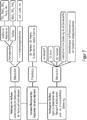
- the first nanoparticles 11 1 , 11 2 , 113 of the first nanoparticle structure 11 and the second nanoparticles 12 1 , 12 2 , 12 3 of the second nanoparticle structure 12 each have the same material, however with a different doping. This is in the lower branch of Figure 7 shown.
- the first nanoparticles 11 1 , 11 2 , 11 3 of the first nanoparticle structure 11 and the second nanoparticles 12 1 , 12 2 , 12 3 of the second nanoparticle structure 12 each have the same material which is an element of the main chemical group IV contains. These include carbon (C), silicon (Si) or germanium (Ge). In principle, different doping with dopants can be provided. In addition, it would be conceivable to additionally provide the nanoparticle structures 11, 12 with coatings, for example made of polymers, in order to protect them from external influences (for example oxidation).
- Nanoparticle structures are to be realized which are characterized by the generation of intrinsically non-linearly amplified electrical signals as soon as the corresponding molecules are attached to the surface of the nanoparticles (NP).
- the non-linear amplification should make it possible to achieve a signal even when the concentration of the molecules is very low, although there is no need to be proportional to the concentration.
- a signal cascade should start and end in a defined maximum signal peak. This would be advantageously used in sensor technology. With this characteristic, the structures would also be able to simulate the behavior of biological nerve cells.
- the structure with nanoparticles results in layers that are open to diffusion and into which molecules can diffuse.
- One form of implementation are horizontally layered nanoparticles with pn junctions in the contact area of the different materials ( Figure 5A ).
- a diode characteristic is achieved with two layers. However, more than two layers can also be layered. With triple layering, a transistor structure is possible (npn, pnp).
- Quadruple stratification basically provides the structure of thyristors.
- Chalcogenides are the compounds of transition metals with Group VI elements (O, S, Se, Te).
- Compounds that can be envisaged for this invention are, for example: TiO 2 , WO 3 , MoO 3 , ZnO, Fe 2 O 3 , WS 2 , MoS 2 . These connections have the electrical conductivity of semiconductors.
- a III-V compound semiconductor is a combination of materials from main chemical group III (earth metals / boron group) and V (nitrogen-phosphorus group), the combination of which also has the electrical conductivity of semiconductors.
- the invention creates self-organized pn junctions with direct contact to the media to be examined. This enables an inexpensive construction with high sensitivity, as well as a large active, inner surface by using nanoparticles. In addition, a large-scale construction on any substrates is possible. Furthermore, the generally high processing temperatures (600 ° C) can be used for stoichiometric compounds. A simple combination of generally incompatible connections due to incompatible manufacturing processes (for example oxidic source / drain layers with a sulfidic base of for example MoS 2 placed in between) is possible.
Landscapes
- Engineering & Computer Science (AREA)
- Microelectronics & Electronic Packaging (AREA)
- Power Engineering (AREA)
- Chemical & Material Sciences (AREA)
- Physics & Mathematics (AREA)
- General Physics & Mathematics (AREA)
- Ceramic Engineering (AREA)
- Condensed Matter Physics & Semiconductors (AREA)
- Computer Hardware Design (AREA)
- Nanotechnology (AREA)
- Crystallography & Structural Chemistry (AREA)
- Electrochemistry (AREA)
- Immunology (AREA)
- Health & Medical Sciences (AREA)
- Life Sciences & Earth Sciences (AREA)
- Analytical Chemistry (AREA)
- Biochemistry (AREA)
- General Health & Medical Sciences (AREA)
- Chemical Kinetics & Catalysis (AREA)
- Pathology (AREA)
- Manufacturing & Machinery (AREA)
- Materials Engineering (AREA)
- Mathematical Physics (AREA)
- Theoretical Computer Science (AREA)
- Light Receiving Elements (AREA)
Abstract
Die vorliegende Erfindung betrifft ein nanopartikelbasiertes Halbleiter-Strukturelement (10) mit einer ersten Nanopartikelstruktur (11) mit einer Vielzahl von ersten Nanopartikeln (11<sub>1</sub>, 11<sub>2</sub>, 11<sub>3</sub>) und einer zweiten Nanopartikelstruktur (12) mit einer Vielzahl von zweiten Nanopartikeln (12<sub>1</sub>, 12<sub>2</sub>, 12<sub>3</sub>). Die erste Nanopartikelstruktur (11) und die zweite Nanopartikelstruktur (12) sind direkt aneinander angrenzend angeordnet, sodass zumindest ein Teil der ersten Nanopartikel (11<sub>1</sub>, 11<sub>2</sub>, 11<sub>3</sub>) und zumindest ein Teil der zweiten Nanopartikel (12<sub>1</sub>, 12<sub>2</sub>, 12<sub>3</sub>) in direktem Kontakt miteinander sind, wobei sich an den jeweiligen Kontaktpunkten von ersten und zweiten Nanopartikeln (11<sub>1</sub>, 11<sub>2</sub>, 11<sub>3</sub>, 12<sub>1</sub>, 12<sub>2</sub>, 12<sub>3</sub>) ein p-n-Übergang mit einer vorbestimmten Raumladungszone ausbildet.The present invention relates to a nanoparticle-based semiconductor structural element (10) with a first nanoparticle structure (11) with a large number of first nanoparticles (11 <sub> 1 </sub>, 11 <sub> 2 </sub>, 11 <sub> 3 </sub>) and a second nanoparticle structure (12) with a multiplicity of second nanoparticles (12 <sub> 1 </sub>, 12 <sub> 2 </sub>, 12 <sub> 3 </sub>) . The first nanoparticle structure (11) and the second nanoparticle structure (12) are arranged directly adjacent to one another, so that at least some of the first nanoparticles (11 <sub> 1 </sub>, 11 <sub> 2 </sub>, 11 <sub > 3 </sub>) and at least some of the second nanoparticles (12 <sub> 1 </sub>, 12 <sub> 2 </sub>, 12 <sub> 3 </sub>) are in direct contact with each other , where at the respective contact points of first and second nanoparticles (11 <sub> 1 </sub>, 11 <sub> 2 </sub>, 11 <sub> 3 </sub>, 12 <sub> 1 </ sub>, 12 <sub> 2 </sub>, 12 <sub> 3 </sub>) forms a pn junction with a predetermined space charge zone.
Description
Die Erfindung betrifft ein Halbleiter-Strukturelement, und insbesondere ein nanopartikelbasiertes Halbleiter-Strukturelement.The invention relates to a semiconductor structure element, and in particular to a nanoparticle-based semiconductor structure element.
Halbleiterschaltungen sind hinlänglich bekannt und weisen mindestens ein halbleitendes Material und mindestens einen p-n-Übergang auf. Eine oder mehrere derartige Halbleiterschaltungen können in Halbleiterstrukturen integriert sein. Diese Halbleiterstrukturen können eindimensionale, zweidimensionale oder dreidimensionale Formen aufweisen und daher auch als Halbleiter-Strukturelemente bezeichnet werden. Diese werden für gewöhnlich eingesetzt, um beispielsweise elektronische Bauteile herzustellen. Beispielsweise werden derartige Halbleiter-Strukturelemente heutzutage im Bereich der Sensorik genutzt. Aufgrund der geringen, und teilweise mikroskopisch kleinen Abmessungen halbleiterbasierter Sensoren sind die erzeugbaren Signalpegel verhältnismäßig gering. Daher müssen derartige Halbleiter-Strukturelemente hochpräzise gefertigt werden, was jedoch mit hohen Herstellungskosten verbunden ist.Semiconductor circuits are well known and have at least one semiconducting material and at least one p-n junction. One or more such semiconductor circuits can be integrated in semiconductor structures. These semiconductor structures can have one-dimensional, two-dimensional or three-dimensional shapes and can therefore also be referred to as semiconductor structure elements. These are usually used to manufacture electronic components, for example. For example, such semiconductor structural elements are used today in the field of sensors. Due to the small and sometimes microscopic dimensions of semiconductor-based sensors, the signal levels that can be generated are relatively low. Therefore, such semiconductor structural elements have to be manufactured with high precision, but this is associated with high manufacturing costs.
Außerdem müssen die sehr geringen Signalpegel in der Regel verstärkt werden, bevor die Signale ausgewertet werden können. Bei der auf Halbleitertechnik basierenden Detektion von Licht wird beispielsweise eine intrinsische Verstärkung durch Avalanche-Vervielfältigung von elektrischen Ladungsträgern verwendet. Dort liegt eine Beschleunigungsspannung über einem Bauelementbereich, in dem durch Licht die elektrischen Ladungsträger erzeugt und durch nachfolgende ionisierende Stöße vervielfältigt werden. Dies lässt sich allerdings so nicht auf die elektrochemische Sensorstruktur übertragen.In addition, the very low signal levels usually have to be amplified before the signals can be evaluated. In the detection of light based on semiconductor technology, for example, an intrinsic amplification by avalanche multiplication of electrical charge carriers is used. There is an acceleration voltage over a component area in which the electrical charge carriers are generated by light and multiplied by subsequent ionizing impacts. However, this cannot be transferred to the electrochemical sensor structure.
Bei der chemischen Sensorik kann das Prinzip der intrinsischen Verstärkung hingegen nicht ohne weiteres adaptiert werden. Je nachdem auf welchen chemischen Bestandteil die halbleiterbasierte Sensorik responsiv sein soll, müssen bei der Herstellung eines konventionellen chemischen Halbleiter-Sensors teilweise sehr hohe Prozessierungstemperaturen (> 600°C) angewendet werden, um geeignete stöchiometrische Verbindungen zu schaffen. Bei diesen hohen Prozessierungstemperaturen besteht jedoch die Gefahr, dass die halbleiterbasierte Sensorschicht irreparabel geschädigt wird. Außerdem würden, je nachdem welcher chemische Bestandteil gemessen werden soll, Materialverbindungen benötigt, die jedoch aufgrund inkompatibler konventioneller Herstellungsprozesse nicht miteinander kombinierbar sind, wie z.B. oxidische Schichten mit einer dazwischen angeordneten Sulfidschicht. Aus diesem Grund wird im Bereich der halbleiterbasierten chemischen Sensorik heutzutage nicht mit intrinsischer Verstärkung sondern mit einer nachgeschalteten Verstärkung des Sensorsignals gearbeitet, z.B. unter Verwendung von geeigneten Verstärkerschaltungen und mit einer möglichst rauscharmen proportionalen Signalvervielfachung.In the chemical sensor technology, however, the principle of intrinsic amplification cannot be easily adapted. Depending on the chemical constituent to which the semiconductor-based sensor system should be responsive, very high processing temperatures (> 600 ° C) must be used in some cases in order to create suitable stoichiometric connections when producing a conventional chemical semiconductor sensor. At these high processing temperatures, however, there is a risk that the semiconductor-based sensor layer will be irreparably damaged. In addition, depending on which chemical component is to be measured, material compounds would become required, which, however, cannot be combined with one another due to incompatible conventional manufacturing processes, such as, for example, oxide layers with a sulfide layer arranged between them. For this reason, in the field of semiconductor-based chemical sensor technology, it is nowadays not with intrinsic amplification but with a downstream amplification of the sensor signal, for example using suitable amplifier circuits and with a signal multiplication that is as low-noise as possible.
Es wäre demnach wünschenswert, ein Halbleiter-Strukturelement bereitzustellen, das diverse Materialkombinationen ermöglicht, um einen breiten Einsatzbereich abzudecken, und dabei trotzdem kostengünstig herstellbar ist und gleichzeitig eine hohe Signalqualität liefert.Accordingly, it would be desirable to provide a semiconductor structure element that enables various material combinations to cover a wide range of uses, and yet is inexpensive to produce and at the same time delivers high signal quality.
Daher wird ein Halbleiter-Strukturelement mit den Merkmalen von Anspruch 1 vorgeschlagen. Ausführungsformen und weitere vorteilhafte Aspekte dieses Halbleiter-Strukturelements sind in den jeweils abhängigen Patentansprüchen genannt.A semiconductor structural element having the features of claim 1 is therefore proposed. Embodiments and further advantageous aspects of this semiconductor structural element are mentioned in the respective dependent claims.
Das erfindungsgemäße Halbleiter-Strukturelement basiert auf Nanopartikeln. Nanopartikel, die auch als Nanoteilchen bezeichnet werden können, definieren sich durch ihre Größe, die typischerweise zwischen 1 bis 100 Nanometern liegt. Das Halbleiter-Strukturelement hat eine eindimensionale, zweidimensionale oder dreidimensionale Form und weist eine Vielzahl derartiger Nanopartikeln auf. Genauer gesagt weist das Halbleiter-Strukturelement eine erste Nanopartikelstruktur mit einer Vielzahl von ersten Nanopartikeln, sowie eine zweite Nanopartikelstruktur mit einer Vielzahl von zweiten Nanopartikeln auf. Die Nanopartikel können innerhalb der jeweiligen Nanopartikelstruktur lose vorliegen oder fest miteinander verbunden sein. Die Nanopartikelstrukturen können beispielsweise in Form einer Schicht, eines Flake-Körpers oder anderer Strukturen vorliegen. Die Nanopartikelstrukturen können demnach ihrerseits ganz allgemein eine eindimensionale, zweidimensionale oder dreidimensionale Form aufweisen. Erfindungswesentlich ist jedoch, dass die erste Nanopartikelstruktur und die zweite Nanopartikelstruktur direkt aneinander angrenzend angeordnet sind, und zwar so, dass zumindest ein Teil der ersten Nanopartikel und zumindest ein Teil der zweiten Nanopartikel in direktem Kontakt miteinander sind. Dies führt dazu, dass sich an den jeweiligen Kontaktpunkten von ersten und zweiten Nanopartikeln ein p-n-Übergang mit einer vorbestimmten Raumladungszone ausbildet. Gleichbedeutend mit einem p-n-Übergang ist selbstverständlich auch ein n-p-Übergang, der somit ebenfalls im Sinne der vorliegenden Offenbarung eingeschlossen ist. Die vorbestimmte Raumladungszone zwischen den beiden Nanopartikelstrukturen bedingt einen entsprechend vorbestimmten Leitwert des Halbleiter-Strukturelements. Die Nanopartikel innerhalb der Nanopartikelstrukturen führen dazu, dass die jeweilige Nanopartikelstruktur ein verhältnismäßig großes Oberflächen-Volumen-Verhältnis aufweist. Demnach bieten die Nanopartikelstrukturen eine deutliche größere aktive Oberfläche im Vergleich zu konventionellen Halbleiterstrukturen bei gleichem Volumen. Aufgrund der erhöhten aktiven Oberfläche weist das erfindungsgemäße nanopartikelbasierte Halbleiter-Strukturelement eine deutlich höhere Empfindlichkeit im Vergleich zu konventionellen, gleich großen, Halbleiterstrukturen auf. Ein weiterer Vorteil der Nanopartikelstrukturen besteht darin, dass ein einfacher physischer Kontakt zwischen der ersten und der zweiten Nanopartikelstruktur bereits ausreichend ist, um an der Kontaktstelle einen p-n-Übergang auszubilden. Das heißt, die im Stand der Technik üblichen hohen Prozessierungstemperaturen (> 600°C), die zum Herstellen von stöchiometrischen Verbindungen zwischen zwei konventionellen (nicht nanopartikelbasierten) Halbleitermaterialien benötigt werden, können vermieden werden. Zudem können mit der vorliegenden Erfindung auch Verbindungen von Materialien, die ansonsten aufgrund nicht-kompatibler Herstellungsprozesse nicht oder nur unter erschwerten Bedingungen miteinander kombinierbar wären, realisiert werden.The semiconductor structural element according to the invention is based on nanoparticles. Nanoparticles, which can also be called nanoparticles, are defined by their size, which is typically between 1 and 100 nanometers. The semiconductor structural element has a one-dimensional, two-dimensional or three-dimensional shape and has a large number of such nanoparticles. More precisely, the semiconductor structure element has a first nanoparticle structure with a multiplicity of first nanoparticles, and also a second nanoparticle structure with a multiplicity of second nanoparticles. The nanoparticles can be loosely present within the respective nanoparticle structure or be firmly connected to one another. The nanoparticle structures can, for example, be in the form of a layer, a flake body or other structures. Accordingly, the nanoparticle structures themselves can generally have a one-dimensional, two-dimensional or three-dimensional shape. It is essential to the invention, however, that the first nanoparticle structure and the second nanoparticle structure are arranged directly adjacent to one another, in such a way that at least some of the first nanoparticles and at least some of the second nanoparticles are in direct contact with one another. As a result, a pn junction with a predetermined space charge zone is formed at the respective contact points of first and second nanoparticles. Synonymous with a pn transition is of course also an np transition, which is thus also included in the sense of the present disclosure. The predetermined space charge zone between the two nanoparticle structures requires one corresponding to the predetermined conductance of the semiconductor structure element. The nanoparticles within the nanoparticle structures result in the respective nanoparticle structure having a relatively large surface-to-volume ratio. Accordingly, the nanoparticle structures offer a significantly larger active surface compared to conventional semiconductor structures with the same volume. Due to the increased active surface, the nanoparticle-based semiconductor structure element according to the invention has a significantly higher sensitivity compared to conventional semiconductor structures of the same size. Another advantage of the nanoparticle structures is that a simple physical contact between the first and the second nanoparticle structure is already sufficient to form a pn junction at the contact point. This means that the high processing temperatures (> 600 ° C.) customary in the prior art, which are required for producing stoichiometric connections between two conventional (non-nanoparticle-based) semiconductor materials, can be avoided. In addition, the present invention can also be used to connect materials that would otherwise not be combinable with one another due to incompatible manufacturing processes, or that could only be combined under difficult conditions.
Gemäß einem Ausführungsbeispiel kann die erste Nanopartikelstruktur und/oder die zweite Nanopartikelstruktur eine diffusionsoffene (innere) Struktur aufweisen, in welche Moleküle aus der Umgebung eindiffundieren können. Wie eingangs erwähnt, können die Nanopartikel innerhalb der jeweiligen Nanopartikelstruktur derart aneinander angelagert sein, dass sich eine poröse Struktur ausbildet. Demnach kann die gesamte Nanopartikelstruktur innen sowie außen eine poröse Struktur aufweisen. Dies wiederum erhöht das Oberflächen-Volumen-Verhältnis der aktiven, inneren Oberfläche der jeweiligen Nanopartikelstruktur.According to one exemplary embodiment, the first nanoparticle structure and / or the second nanoparticle structure can have a diffusion-open (inner) structure, into which molecules can diffuse from the environment. As mentioned at the beginning, the nanoparticles can be attached to one another within the respective nanoparticle structure in such a way that a porous structure is formed. Accordingly, the entire nanoparticle structure can have a porous structure inside and outside. This in turn increases the surface-volume ratio of the active, inner surface of the respective nanoparticle structure.
Gemäß einem weiteren Ausführungsbeispiel kann das nanopartikelbasierte Halbleiter-Strukturelement derart ausgestaltet sein, dass sich die vorbestimmte Raumladungszone und somit ein vorbestimmter Leitwert des nanopartikelbasierten Halbleiter-Strukturelements verändert, wenn sich eindiffundierte Moleküle an der Oberfläche von in der jeweiligen Nanopartikelstruktur enthaltenen Nanopartikeln anlagern. Die sich anlagernden Moleküle beeinflussen somit direkt den p-n-Übergang zwischen sich gegenseitig kontaktierenden Nanopartikeln der ersten und zweiten Nanopartikelstrukturen. Das heißt, die Raumladungszone des p-n-Übergangs wird größer oder kleiner. Dies führt dementsprechend zu einer Änderung des Leitwerts des Halbleiter-Strukturelements, d.h. der Leitwert wird ebenfalls größer oder kleiner. Aufgrund des großen Oberflächen-Volumen-Verhältnisses der Nanopartikelstrukturen können sich (im Vergleich zu konventionellen, nicht nanopartikelbasierten Halbleiterstrukturen) relativ viele Moleküle an der aktiven Oberfläche anlagern. Je mehr Moleküle sich an der aktiven Oberfläche anlagern, desto stärker fällt die Änderung des Leitwerts aus. Dies kann vorteilhaft für elektrochemische Sensorik verwendet werden.According to a further exemplary embodiment, the nanoparticle-based semiconductor structure element can be configured such that the predetermined space charge zone and thus a predetermined conductance of the nanoparticle-based semiconductor structure element change when molecules which have diffused accumulate on the surface of nanoparticles contained in the respective nanoparticle structure. The attached molecules thus directly influence the pn junction between mutually contacting nanoparticles of the first and second nanoparticle structures. That is, the space charge zone of the pn junction becomes larger or smaller. This accordingly leads to a change in the conductance of the semiconductor structure element, ie the conductance also becomes larger or smaller. Due to the large surface-volume ratio of the nanoparticle structures (compared to conventional, non-nanoparticle-based semiconductor structures), a relatively large number of molecules can accumulate on the active surface. The more molecules that accumulate on the active surface, the greater the change in the conductance. This can be used advantageously for electrochemical sensors.
Gemäß einem weiteren Ausführungsbeispiel kann das Halbleiter-Strukturelement eine Auswerteschaltung aufweisen oder mit einer solchen verbunden werden, wobei die erste und/oder die zweite Nanopartikelstruktur eine elektrochemische Sensorstruktur bereitstellt, wobei Moleküle eines Analyten in diese elektrochemische Sensorstruktur eindiffundieren und sich an der Oberfläche von darin befindlichen Nanopartikeln anlagern können, um die vorbestimmte Raumladungszone und somit einen vorbestimmten Leitwert des nanopartikelbasierten Halbleiter-Strukturelements zu verändern, und wobei die Auswertevorrichtung ausgestaltet ist, um basierend auf der Änderung des Leitwerts den Analyten zu bestimmen. Wie eingangs erwähnt, kann also mittels des erfindungsgemäßen Halbleiter-Strukturelements ein elektrochemischer Sensor realisiert werden. Die erste und/oder zweite Nanopartikelstruktur können dabei eine elektrochemische Sensorschicht bereitstellen, an der sich Moleküle eines Analyten anlagern können. Je nach Typ des Analyten stellt sich ein anderer Leitwert ein, anhand dessen der Analyt bestimmt werden kann. Da sich aufgrund der porösen Struktur der Nanopartikelstrukturen verhältnismäßig viele Moleküle an der aktiven Oberfläche anlagern können, können auch unterschiedliche Typen von Analyten mit hoher Genauigkeit bzw. Empfindlichkeit bestimmt und voneinander unterschieden werden.According to a further exemplary embodiment, the semiconductor structure element can have or be connected to an evaluation circuit, the first and / or the second nanoparticle structure providing an electrochemical sensor structure, molecules of an analyte diffusing into this electrochemical sensor structure and being located on the surface thereof Nanoparticles can accumulate in order to change the predetermined space charge zone and thus a predetermined conductivity of the nanoparticle-based semiconductor structure element, and the evaluation device is designed to determine the analyte based on the change in the conductivity. As mentioned at the beginning, an electrochemical sensor can therefore be implemented by means of the semiconductor structural element according to the invention. The first and / or second nanoparticle structure can provide an electrochemical sensor layer on which molecules of an analyte can accumulate. Depending on the type of analyte, a different conductance arises, based on which the analyte can be determined. Since a relatively large number of molecules can accumulate on the active surface due to the porous structure of the nanoparticle structures, different types of analytes can also be determined and distinguished from one another with high accuracy or sensitivity.
Gemäß einem weiteren Ausführungsbeispiel kann das nanopartikelbasierte Halbleiter-Strukturelement ausgestaltet sein, um ein Signal mit intrinsisch nicht-linearer Verstärkung zu erzeugen. Das heißt, das erfindungsgemäße Halbleiter-Strukturelement benötigt im Vergleich zu konventionellen, nicht nanopartikelbasierten, Halbleitern keine extrinsische Signalverstärkung. Zudem kann die sich an den einzelnen Nanopartikeln ausbildende Vielzahl von p-n-Übergängen dafür sorgen, dass es zu einer nicht-linearen Signalverstärkung kommt. Beispielsweise kann eine sich selbst verstärkende Signalverstärkungswirkung eintreten, vergleichbar mit dem Avalanche-Effekt bei Photodioden.According to a further exemplary embodiment, the nanoparticle-based semiconductor structure element can be designed to generate a signal with intrinsically non-linear amplification. This means that the semiconductor structural element according to the invention does not require any extrinsic signal amplification in comparison to conventional semiconductors which are not based on nanoparticles. In addition, the large number of p-n junctions that form on the individual nanoparticles can ensure that non-linear signal amplification occurs. For example, a self-amplifying signal amplification effect can occur, comparable to the avalanche effect in photodiodes.
Gemäß einem weiteren Ausführungsbeispiel können die ersten Nanopartikel der ersten Nanopartikelstruktur und die zweiten Nanopartikel der zweiten Nanopartikelstruktur jeweils unterschiedliche Materialien aufweisen, die sich in der Höhe der Austrittsarbeiten für Elektronen und/oder in der Höhe der jeweiligen Bandlücke voneinander unterscheiden. Das heißt, das Halbleiter-Strukturelement weist einen heterogenen Aufbau auf, wobei die ersten Nanopartikel der ersten Nanopartikelstruktur und die zweiten Nanopartikel der zweiten Nanopartikelstruktur unterschiedliche Materialien aufweisen können. Diese unterschiedlichen Materialien sind vorzugsweise unterschiedliche Halbleitermaterialien, sodass es an den Kontaktstellen zwischen den Nanopartikeln unterschiedlicher Materialien zu elektronischen Übergängen mit p-n-Charakteristik bzw. n-p-Charakteristik kommt.According to a further exemplary embodiment, the first nanoparticles of the first nanoparticle structure and the second nanoparticles of the second nanoparticle structure can each have different materials which differ from one another in the height of the work functions for electrons and / or in the height of the respective band gap. This means that the semiconductor structure element has a heterogeneous structure, wherein the first nanoparticles of the first nanoparticle structure and the second nanoparticles of the second nanoparticle structure can have different materials. These different materials are preferably different semiconductor materials, so that electronic transitions with pn or np characteristics occur at the contact points between the nanoparticles of different materials.
Gemäß einem weiteren Ausführungsbeispiel können die ersten Nanopartikel der ersten Nanopartikelstruktur und die zweiten Nanopartikel der zweiten Nanopartikelstruktur jeweils unterschiedliche Materialien aus der chemischen Hauptgruppe VI, die auch als Chalkogene bezeichnet werden, aufweisen. Hierzu zählen Sauerstoff (O), Schwefel (S), Selen (Se), Tellur (Te), sowie Polonium (Po) und Livermorium (Lv).According to a further exemplary embodiment, the first nanoparticles of the first nanoparticle structure and the second nanoparticles of the second nanoparticle structure can each have different materials from the main chemical group VI, which are also referred to as chalcogens. These include oxygen (O), sulfur (S), selenium (Se), tellurium (Te), as well as polonium (Po) and livermorium (Lv).
Gemäß einem weiteren Ausführungsbeispiel können die ersten Nanopartikel der ersten Nanopartikelstruktur und die zweiten Nanopartikel der zweiten Nanopartikelstruktur jeweils unterschiedliche Materialverbindungen mit jeweils mindestens einem Element der chemischen Hauptgruppe VI und mindestens einem Übergangsmetall aufweisen, wobei diese Materialverbindungen auch als Chalkogenide bezeichnet werden und die elektrische Leitfähigkeit von Halbleitern aufweisen. Chalkogenide sind chemische Verbindungen aus einem oder mehreren Chalkogen-Elementen (insbesondere Sauerstoff, Schwefel, Selen und Tellur) als formale Anionen mit Metallen oder stärker elektropositiven Elementen (Arsen, Germanium, Phosphor, Antimon, Blei, Bor, Aluminium, Gallium, Indium, Titan, Natrium) als formale Kationen. Für die erfindungsgemäßen Nanopartikelstrukturen werden vorzugsweise Übergangsmetalle als Reaktionspartner mit den Chalkogen-Elementen verwendet, da diese eine Elektronenkonfiguration besitzen, so dass sich eine halb-leitende Eigenschaft der Materialverbindung einstellt. Die chemischen Elemente mit den Ordnungszahlen von 21 bis 30, 39 bis 48, 57 bis 80 und 89 bis 112 werden üblicherweise als Übergangselemente bezeichnet. Da diese Elemente alle Metalle sind, wird auch der Ausdruck Übergangsmetalle benutzt.According to a further exemplary embodiment, the first nanoparticles of the first nanoparticle structure and the second nanoparticles of the second nanoparticle structure can each have different material connections, each with at least one element from main chemical group VI and at least one transition metal, these material connections also being called chalcogenides and the electrical conductivity of semiconductors exhibit. Chalcogenides are chemical compounds of one or more chalcogen elements (especially oxygen, sulfur, selenium and tellurium) as formal anions with metals or more electropositive elements (arsenic, germanium, phosphorus, antimony, lead, boron, aluminum, gallium, indium, titanium , Sodium) as formal cations. For the nanoparticle structures according to the invention, transition metals are preferably used as reactants with the chalcogen elements, since these have an electron configuration, so that a semi-conductive property of the material connection is established. The chemical elements with the atomic numbers from 21 to 30, 39 to 48, 57 to 80 and 89 to 112 are usually referred to as transition elements. Since these elements are all metals, the term transition metals is also used.
Gemäß einem weiteren Ausführungsbeispiel können die ersten Nanopartikel der ersten Nanopartikelstruktur und/oder die zweiten Nanopartikel der zweiten Nanopartikelstruktur eine oxidische Materialverbindung aus Sauerstoff und einem Übergangsmetall aufweisen. Eine solche Chalkogenid-Verbindung mit Sauerstoff ist im Vergleich zu Chalkogenid-Verbindungen mit Selen oder Tellur für manche Anwendungen vorteilhaft, da letztere Chalkogenid-Verbindungen giftig sind.According to a further exemplary embodiment, the first nanoparticles of the first nanoparticle structure and / or the second nanoparticles of the second nanoparticle structure can have an oxidic material compound composed of oxygen and a transition metal. Such a chalcogenide compound with oxygen is advantageous compared to chalcogenide compounds with selenium or tellurium for some applications, since the latter chalcogenide compounds are toxic.
Gemäß einem weiteren Ausführungsbeispiel können die ersten Nanopartikel der ersten Nanopartikelstruktur und/oder die zweiten Nanopartikel der zweiten Nanopartikelstruktur zumindest eine oxidische Materialverbindung aus der Gruppe von ZnO, TiO2, MoO3, WO3 und Fe2O3 aufweisen.According to a further exemplary embodiment, the first nanoparticles of the first nanoparticle structure and / or the second nanoparticles of the second nanoparticle structure can have at least one oxidic material compound from the group of ZnO, TiO 2 , MoO 3 , WO 3 and Fe 2 O 3 .
Gemäß einem weiteren Ausführungsbeispiel können die ersten Nanopartikel der ersten Nanopartikelstruktur und/oder die zweiten Nanopartikel der zweiten Nanopartikelstruktur eine sulfidische Materialverbindung aus Schwefel und einem Übergangsmetall aufweisen. Eine solche Chalkogenid-Verbindung mit Schwefel ist im Vergleich zu Chalkogenid-Verbindungen mit Selen oder Tellur für manche Anwendungen vorteilhaft, da letztere Chalkogenid-Verbindungen giftig sind.According to a further exemplary embodiment, the first nanoparticles of the first nanoparticle structure and / or the second nanoparticles of the second nanoparticle structure can have a sulfidic material compound composed of sulfur and a transition metal. Such a chalcogenide compound with sulfur is advantageous compared to chalcogenide compounds with selenium or tellurium for some applications, since the latter chalcogenide compounds are toxic.
Gemäß einem weiteren Ausführungsbeispiel können die ersten Nanopartikel der ersten Nanopartikelstruktur und/oder die zweiten Nanopartikel der zweiten Nanopartikelstruktur zumindest eine sulfidische Materialverbindung aus der Gruppe von MoS2, WS2 und FeS2 (Eisendisulfid, Pyrith) aufweisen.According to a further exemplary embodiment, the first nanoparticles of the first nanoparticle structure and / or the second nanoparticles of the second nanoparticle structure can have at least one sulfidic material compound from the group of MoS 2 , WS 2 and FeS 2 (iron disulfide, pyrite).
Gemäß einem weiteren Ausführungsbeispiel können die ersten Nanopartikel der ersten Nanopartikelstruktur ein Material aus der chemischen Hauptgruppe III aufweisen, und die zweiten Nanopartikel der zweiten Nanopartikelstruktur können ein Material aus der chemischen Hauptgruppe V aufweisen. Natürlich ist es ebenfalls möglich, dass die ersten Nanopartikel der ersten Nanopartikelstruktur ein Material aus der chemischen Hauptgruppe V aufweisen, und die zweiten Nanopartikel der zweiten Nanopartikelstruktur ein Material aus der chemischen Hauptgruppe III aufweisen.According to a further exemplary embodiment, the first nanoparticles of the first nanoparticle structure can have a material from the main chemical group III, and the second nanoparticles of the second nanoparticle structure can have a material from the main chemical group V. Of course, it is also possible for the first nanoparticles of the first nanoparticle structure to have a material from the main chemical group V and for the second nanoparticles of the second nanoparticle structure to have a material from the main chemical group III.
Gemäß einem weiteren Ausführungsbeispiel können die ersten Nanopartikel der ersten Nanopartikelstruktur und die zweiten Nanopartikel der zweiten Nanopartikelstruktur jeweils das gleiche Material, jedoch mit einer unterschiedlichen Dotierung, aufweisen. Das heißt, das Halbleiter-Strukturelement weist einen homogenen Aufbau auf, wobei die ersten Nanopartikel der ersten Nanopartikelstruktur und die zweiten Nanopartikel der zweiten Nanopartikelstruktur die gleichen Materialien aufweisen können, wobei diese Materialien vorzugsweise die gleichen Halbleitermaterialien sind. Diese können beispielsweise eine unterschiedliche Dotierung aufweisen, sodass es an den Kontaktstellen zwischen den Nanopartikeln mit unterschiedlicher Dotierung zur Ausbildung von p-n-Übergängen kommt.According to a further exemplary embodiment, the first nanoparticles of the first nanoparticle structure and the second nanoparticles of the second nanoparticle structure can each have the same material, but with a different doping. This means that the semiconductor structure element has a homogeneous structure, wherein the first nanoparticles of the first nanoparticle structure and the second nanoparticles of the second nanoparticle structure can have the same materials, these materials preferably being the same semiconductor materials. These can have different doping, for example, so that p-n junctions are formed at the contact points between the nanoparticles with different doping.
Gemäß einem weiteren Ausführungsbeispiel können die ersten Nanopartikel der ersten Nanopartikelstruktur und die zweiten Nanopartikel der zweiten Nanopartikelstruktur jeweils das gleiche Material aufweisen, welches ein Element der chemischen Hauptgruppe IV enthält. Hierzu zählen unter anderem Kohlenstoff (C), Silizium (Si) oder Germanium (Ge).According to a further exemplary embodiment, the first nanoparticles of the first nanoparticle structure and the second nanoparticles of the second nanoparticle structure can each have the same material which is an element of the main chemical group IV contains. These include carbon (C), silicon (Si) or germanium (Ge).
Gemäß einem weiteren Ausführungsbeispiel können die erste Nanopartikelstruktur und die zweite Nanopartikelstruktur jeweils als eine Nanopartikelschicht ausgeführt sein, wobei diese Nanopartikelschichten in einem Schichtstapel übereinander angeordnet sind. Dies bietet eine einfache Art und Weise, die einzelnen Nanopartikelstrukturen miteinander zu kontaktieren. Das Erstellen von Schichtstapeln mit Nanopartikel beinhaltenden Schichten kann außerdem aus konventionellen Verfahren zum Herstellen von konventionellen, nicht nanopartikelbasierten, Halbleiterstrukturen übernommen werden. Dies bietet eine kostengünstige Adaption bestehender Technik, angewendet auf ein anderes technisches Gebiet.According to a further exemplary embodiment, the first nanoparticle structure and the second nanoparticle structure can each be embodied as a nanoparticle layer, these nanoparticle layers being arranged one above the other in a layer stack. This offers a simple way of contacting the individual nanoparticle structures with one another. The creation of layer stacks with layers containing nanoparticles can also be adopted from conventional methods for producing conventional, non-nanoparticle-based semiconductor structures. This offers a cost-effective adaptation of existing technology, applied to another technical area.
Gemäß einem weiteren Ausführungsbeispiel kann das Halbleiter-Strukturelement eine dritte Nanopartikelschicht mit einer Vielzahl von dritten Nanopartikeln aufweisen, wobei die zweite Nanopartikelschicht zwischen der ersten und der dritten Nanopartikelschicht angeordnet ist, und wobei sich an den jeweiligen Kontaktpunkten von zweiten und dritten Nanopartikeln ein zweiter p-n-Übergang mit einer vorbestimmten Raumladungszone ausbildet. Auch bei diesem zweiten p-n-Übergang gilt sinngemäß, dass dieser natürlich auch einen n-p-Übergang einschließt. Es wird also ein Schichtstapel bereitgestellt, der drei Nanopartikelstrukturen in Form von drei aufeinander gestapelten Nanopartikelschichten aufweist. Dabei kann es denkbar sein, dass die zweite und die dritte Nanopartikelstruktur einen homogenen oder einen heterogenen Aufbau aufweisen, wie dies zuvor mit Bezug auf die erste und zweite Nanopartikelstrukturen beschrieben wurde. Die erste und die dritte Nanopartikelstruktur können das gleiche Material oder unterschiedliche Materialien aufweisen, wobei das Material der dritten Nanopartikelstruktur vorzugsweise ein Halbleitermaterial ist.According to a further exemplary embodiment, the semiconductor structural element can have a third nanoparticle layer with a multiplicity of third nanoparticles, the second nanoparticle layer being arranged between the first and the third nanoparticle layer, and wherein a second pn- Transition forms with a predetermined space charge zone. In the case of this second p-n transition, it also applies that this naturally also includes an n-p transition. A layer stack is thus provided which has three nanoparticle structures in the form of three nanoparticle layers stacked on top of one another. It may be conceivable that the second and third nanoparticle structures have a homogeneous or a heterogeneous structure, as was described above with reference to the first and second nanoparticle structures. The first and the third nanoparticle structure can have the same material or different materials, wherein the material of the third nanoparticle structure is preferably a semiconductor material.
Gemäß einem weiteren Ausführungsbeispiel kann zumindest eine der ersten, zweiten und dritten Nanopartikelschichten mittels entsprechender Strukturierung freigelegt sein, sodass sich in der Umgebung befindliche Moleküle an die jeweils freigelegte Nanopartikelschicht anlagern können. Freigelegt bedeutet in diesem Zusammenhang, dass die jeweilige Nanopartikelschicht eine Strukturierung, z.B. Loch, Graben, etc. aufweist, wobei diese Strukturierung laterale Seitenwände aufweist, die mit der Umgebung in Kontakt bringbar sind. Dies ermöglicht eine laterale Eindiffusion von in der Umgebung befindlichen Molekülen durch ebendiese lateralen Seitenwände. Das heißt, es wird eine mehrseitige Eindiffusion ermöglicht. Im Vergleich dazu ist ohne eine solche Strukturierung keine laterale Diffusion möglich, sondern lediglich eine Eindiffusion von einer Seite (z.B. einer unstrukturierten Oberseite).According to a further exemplary embodiment, at least one of the first, second and third nanoparticle layers can be exposed by means of appropriate structuring, so that molecules located in the environment can attach to the respectively exposed nanoparticle layer. In this context, exposed means that the respective nanoparticle layer has a structuring, for example a hole, a trench, etc., this structuring having lateral side walls which can be brought into contact with the surroundings. This enables lateral diffusion of molecules in the environment through these lateral sidewalls. That means it is a multi-sided diffusion enables. In comparison, no lateral diffusion is possible without such a structuring, but only a diffusion from one side (eg an unstructured upper side).
Gemäß einem weiteren Ausführungsbeispiel kann das nanopartikelbasierte Halbleiter-Strukturelement eine Diodenstruktur mit einem p-n-Übergang, oder eine Transistorstruktur mit zwei p-n-Übergängen, oder eine Thyristorstruktur mit drei p-n-Übergängen bilden.According to a further exemplary embodiment, the nanoparticle-based semiconductor structure element can form a diode structure with a p-n junction, or a transistor structure with two p-n junctions, or a thyristor structure with three p-n junctions.
Gemäß einem weiteren Ausführungsbeispiel kann das nanopartikelbasierte Halbleiter-Strukturelement eine elektrochemische Sensorstruktur sein, wobei die erste Nanopartikelstruktur und die direkt daran angrenzende zweite Nanopartikelstruktur zusammen eine Sensorschicht bilden.According to a further exemplary embodiment, the nanoparticle-based semiconductor structural element can be an electrochemical sensor structure, the first nanoparticle structure and the second nanoparticle structure directly adjacent to it forming a sensor layer.
Ein weiteres Ausführungsbeispiel sieht eine Sensoranordnung mit einem zuvor beschriebenen nanopartikelbasierten Halbleiter-Strukturelement vor.Another exemplary embodiment provides a sensor arrangement with a previously described nanoparticle-based semiconductor structural element.
Einige Ausführungsbeispiele sind exemplarisch in der Zeichnung dargestellt und werden nachstehend erläutert. Es zeigen:
- Fig. 1
- eine schematische Ansicht eines nanopartikelbasierten Halbleiter-Strukturelements mit zwei Nanopartikelstrukturen gemäß einem Ausführungsbeispiel,
- Figs. 2A, 2B
- eine schematische Skizze zur Erläuterung eines nanopartikelbasierten p-n-Übergangs,
- Figs. 3A, 3B
- eine weitere schematische Skizze zur Erläuterung eines weiteren nanopartikelbasierten p-n-Übergangs,
- Figs. 4A-4C
- eine schematische Skizze zur Erläuterung unterschiedlicher elektronischer Charakteristiken, die mittels nanopartikelbasierter p-n-Übergange realisierbar sind,
- Fig. 5A
- ein als Sensoranordnung ausgestaltetes Halbleiter-Strukturelement aufweisend einen Schichtstapel mit drei Nanopartikelstrukturen,
- Fig. 5B
- eine schematische Ansicht eines nanopartikelbasierten Halbleiter-Strukturelements mit drei Nanopartikelstrukturen gemäß einem Ausführungsbeispiel,
- Figs. 6A-6D
- schematische Draufsichten und Schnittansichten von unterschiedlich strukturierten Halbleiter-Strukturelementen gemäß verschiedenen Ausführungsbeispielen, und
- Fig. 7
- ein schematisches Blockdiagramm zur Kategorisierung unterschiedlicher nanopartikelbasierter Halbleiter-Strukturelemente.
- Fig. 1
- 2 shows a schematic view of a nanoparticle-based semiconductor structural element with two nanoparticle structures according to one exemplary embodiment,
- Figs. 2A, 2B
- 1 shows a schematic sketch to explain a nanoparticle-based pn junction,
- Figs. 3A, 3B
- another schematic sketch to explain another nanoparticle-based pn junction,
- Figs. 4A-4C
- 1 shows a schematic sketch to explain different electronic characteristics that can be implemented using nanoparticle-based pn junctions,
- Figure 5A
- a semiconductor structure element configured as a sensor arrangement, comprising a layer stack with three nanoparticle structures,
- Figure 5B
- 2 shows a schematic view of a nanoparticle-based semiconductor structural element with three nanoparticle structures according to one exemplary embodiment,
- Figs. 6A-6D
- schematic plan views and sectional views of differently structured semiconductor structure elements according to different embodiments, and
- Fig. 7
- a schematic block diagram for categorizing different nanoparticle-based semiconductor structural elements.
Im Folgenden werden Ausführungsbeispiele mit Bezug auf die Figuren näher beschrieben, wobei Elemente mit derselben oder ähnlichen Funktion mit denselben Bezugszeichen versehen sind.Exemplary embodiments are described in more detail below with reference to the figures, elements with the same or similar function being provided with the same reference symbols.
Außerdem wird hierin eine Sensoranordnung, und in einigen expliziten Beispielen ein elektrochemischer Sensor, als ein nicht-limitierendes Beispiel für ein erfindungsgemäßes Halbleiter-Strukturelement beschrieben. Selbstverständlich ist das erfindungsgemäße Halbleiter-Strukturelement nicht auf eine solche, lediglich beispielhaft genannte, Sensorik beschränkt.In addition, a sensor arrangement, and in some explicit examples an electrochemical sensor, is described as a non-limiting example of a semiconductor structural element according to the invention. Of course, the semiconductor structural element according to the invention is not limited to such a sensor system, which is only mentioned as an example.
Die erste Nanopartikelstruktur 11 und die zweite Nanopartikelstruktur 12 sind in diesem nicht-limitierenden Ausführungsbeispiel als einlagige zweidimensionale Strukturen ausgeführt, die in etwa vergleichbar sind mit einlagigen Schichten. Die Nanopartikelstrukturen 11, 12 sind jedoch nicht auf zweidimensionale geometrische Formen beschränkt. Die Nanopartikelstrukturen 11, 12 können auch eindimensionale sowie dreidimensionale geometrische Formen aufweisen, beispielsweise in Form von Würfeln, Quadern, Nanotubes und dergleichen. Außerdem können die Nanopartikelstrukturen 11, 12 unterschiedliche geometrische Formen, oder aber jeweils die gleiche geometrische Form, wie in
Die erste Nanopartikelstruktur 11 und die zweite Nanopartikelstruktur 12 sind direkt aneinander angrenzend angeordnet, sodass zumindest ein Teil der ersten Nanopartikel 111, 112, 113 und zumindest ein Teil der zweiten Nanopartikel 121, 122, 123 in direktem Kontakt miteinander sind.The
Dabei bilden sich an den jeweiligen Kontaktpunkten von ersten und zweiten Nanopartikeln 111, 112, 113, 121, 122, 123 ein p-n-Übergang mit einer vorbestimmten Raumladungszone aus. Genauer gesagt kann sich an jedem Kontaktpunkt, an dem ein erstes Nanopartikel 111, 112, 113 ein zweites Nanopartikel 121, 122, 123 physisch kontaktiert, jeweils ein p-n-Übergang ausbilden.A pn junction with a predetermined space charge zone is formed at the respective contact points of first and
Dies soll beispielhaft unter Bezugnahme auf die
Wie in
Wie in
In den
Die
In allen Beispielen kommt es beim Kontakt der jeweiligen Nanopartikel zur Einstellung eines Energie-Gleichgewichts, sodass sich eine vorbestimmte Raumladungszone ausbildet. Diese vorbestimmte Raumladungszone führt dazu, dass das erfindungsgemäße Halbleiter-Strukturelement 10 einen vorbestimmten Leitwert aufweist.In all examples, an energy balance is established when the respective nanoparticles come into contact, so that a predetermined space charge zone is formed. This predetermined space charge zone means that the
Durch Anlagerung von beispielsweise in der Umgebung befindlichen Molekülen an den jeweiligen Nanopartikelstrukturen 11, 12 verschiebt sich die vorbestimmte Raumladungszone und damit der vorbestimmte Leitwert des Halbleiter-Strukturelements 10.Due to the addition of, for example, molecules located in the environment to the
Bedingt durch den Aufbau der Nanopartikelstrukturen 11, 12 weisen diese eine diffusionsoffene äußere sowie innere Struktur auf, sodass die zuvor genannten Moleküle aus der Umgebung in die jeweilige Nanopartikelstruktur 11, 12 eindiffundieren können.Due to the structure of the
Dabei ist das nanopartikelbasierte Halbleiter-Strukturelement 10 derart ausgestaltet, dass sich die vorbestimmte Raumladungszone und somit der vorbestimmte Leitwert des nanopartikelbasierten Halbleiter-Strukturelements 10 verändert, wenn sich eindiffundierte Moleküle an der Oberfläche von in der jeweiligen Nanopartikelstruktur 11, 12 enthaltenen Nanopartikeln 111, 112, 113, 121, 122, 123 anlagern.The nanoparticle-based
Dies kann vorteilhaft für beispielsweise elektrochemische Sensorik-Anwendungen genutzt werden, um beispielsweise einen bestimmten Analyten zu bestimmen. Je nachdem, welche Stoff-Moleküle sich an den jeweiligen Nanopartikeln 111, 112, 113, 121, 122, 123 anlagern, verändert sich die vorbestimmte Raumladungszone und somit der vorbestimmte Leitwert des Halbleiter-Strukturelements 10 in unterschiedlichem Maße. Dies wiederum ist ein charakteristisches Indiz für den jeweiligen Stoff des angelagerten Moleküls, sodass dieser Stoff als Analyt bestimmt werden kann. Dies kann mit einer entsprechenden Auswertevorrichtung durchführbar sein.This can be used advantageously, for example, for electrochemical sensor applications, for example to determine a specific analyte. Depending on which substance molecules accumulate on the
Dementsprechend sehen Ausführungsbeispiele vor, dass das nanopartikelbasierte Halbleiter-Strukturelement 10 eine Auswertevorrichtung aufweisen kann, oder zumindest an eine solche Auswertevorrichtung anschließbar ist, wobei die erste und/oder die zweite Nanopartikelstruktur 11, 12 (gemeinsam oder jeweils einzeln) eine elektrochemische Sensorstruktur bereitstellen, wobei Moleküle eines Analyten in diese elektrochemische Sensorstruktur eindiffundieren und sich an der Oberfläche von darin befindlichen Nanopartikeln 111, 112, 113, 121, 122, 123 anlagern können, um die vorbestimmte Raumladungszone und somit den vorbestimmten Leitwert des nanopartikelbasierten Halbleiter-Strukturelements 10 zu verändern. Die Auswertevorrichtung kann dementsprechend dazu ausgestaltet sein, um basierend auf der Änderung des Leitwerts den Analyten zu bestimmen.Accordingly, exemplary embodiments provide that the nanoparticle-based
Basierend auf dem jeweiligen Analyten wird ein dementsprechendes Signal von dem Halbleiter-Strukturelement 10 erzeugt. Ein Vorteil des erfindungsgemäßen nanopartikelbasierten Halbleiter-Strukturelements 10 besteht dabei darin, dass dieses derart ausgestaltet sein kann, um ein Signal mit intrinsisch nicht-linearer Verstärkung zu erzeugen.A corresponding signal is generated by the
Dies ist etwas genauer in
Das in
Ferner optional kann zwischen dem Substrat 51 und dem Schichtstapel 50 eine elektrisch leitfähige Beschichtung 52 vorgesehen sein. Diese kann beispielsweise zur Ankontaktierung des Halbleiter-Strukturelements 10 dienen. Die elektrisch leitfähige Beschichtung 52 kann beispielsweise einen oder mehrere Bestandteile aus der Gruppe von Indium-Zinnoxid (ITO), Fluor-dotiertem-Zinnoxid (FTO) und Metall aufweisen. Außerdem kann die elektrisch leitfähige Beschichtung 52 ebenfalls transparent sein.Furthermore, an electrically
Ferner optional kann eine weitere elektrisch leitfähige Beschichtung 56 vorgesehen sein. Diese kann beispielsweise auf der dem Substrat 51 gegenüberliegenden Seite des Schichtstapels 50 angeordnet sein und zur Ankontaktierung des Halbleiter-Strukturelements 10 dienen. Die weitere elektrisch leitfähige Beschichtung 56 kann beispielsweise einen oder mehrere Bestandteile aus der Gruppe von Indium-Zinnoxid (ITO), Fluor-dotiertem-Zinnoxid (FTO) und Metall aufweisen. Außerdem kann die weitere elektrisch leitfähige Beschichtung 52 ebenfalls transparent sein.Furthermore, a further electrically
Der Schichtstapel 50 selbst kann in diesem Falle, wie zuvor beschrieben, eine Transistorcharakteristik aufweisen. Dabei kann die in der Mitte liegende zweite Nanopartikelschicht 12 als elektrische Basis dienen. Die erste Nanopartikelschicht 11 und die dritte Nanopartikelschicht 13 können jeweils entweder als elektrische Source oder Drain (bzw. anders herum) dienen.In this case, the
Sofern die weitere, bzw. obere, elektrisch leitfähige Beschichtung 56 porös ist, so können in der Umgebung befindliche Moleküle durch diese poröse Beschichtung 56 hindurch diffundieren und an die darunter liegende dritte Nanopartikelstruktur 13 gelangen, um sich dort an der Oberfläche der darin enthaltenen Nanopartikel anzulagern. Hierfür kann die weitere elektrisch leitfähige Beschichtung 56 beispielsweise ebenfalls als eine poröse Nanopartikelstruktur ausgeführt sein. Denkbar wären Ausgestaltungen beinhaltend Metall-Nanopartikel, ITO-Nanopartikel oder FTO-Nanopartikel.If the further or upper, electrically
Falls die weitere, bzw. obere, elektrisch leitfähige Beschichtung 56 nicht porös sein sollte, so können in der Umgebung befindliche Moleküle nicht bzw. nur erschwert durch diese poröse Beschichtung 56 hindurch diffundieren. Aus diesem Grund sehen Ausführungsbeispiele vor, das Halbleiter-Strukturelement 10 entsprechend zu strukturieren. Dies kann beispielsweise mittels in der Halbleitertechnik etablierter Prozesse, wie beispielsweise Lithografie, erfolgen. Einige nicht-limitierende Ausführungsbeispiele solcher strukturierter Halbleiter-Strukturelemente 10 sollen nachfolgend unter Bezugnahme auf die
Die
In dem in
In dem in
In dem in
Die soeben beschriebenen Ausführungsbeispiele sehen also allesamt vor, dass zumindest eine der ersten, zweiten und dritten Nanopartikelschichten 11, 12, 13 mittels entsprechender Strukturierung freigelegt ist, sodass sich in der Umgebung befindliche Moleküle an die jeweils freigelegte Nanopartikelschicht 11, 12, 13 anlagern können. Dies gilt natürlich nicht nur für Nanopartikelschichten, sondern generell auch für jegliche Nanopartikelstrukturen im Sinne der vorliegenden Offenbarung, d.h. unabhängig von deren geometrischen Form und Ausgestaltung.The exemplary embodiments just described therefore all provide that at least one of the first, second and third nanoparticle layers 11, 12, 13 is exposed by means of appropriate structuring, so that molecules located in the environment can attach to the respectively exposed
Ein wichtiges Kriterium zur Realisierung des hierin beschriebenen Halbleiter-Strukturelements 10 ist die Materialwahl, insbesondere für die Nanopartikelstrukturen 11, 12, 13. Nachfolgend sollen daher unterschiedliche Materialkompositionen beschrieben werden, wobei diese als nicht abschließende Beispiele zu verstehen sind.
Zunächst kann das nanopartikelbasierte Halbleiter-Strukturelement 10 unterschiedliche Nanopartikelstrukturen 11, 12, 13 aufweisen, die entsprechend ihrem jeweiligen Phänotypus untergliedert werden können. Wie eingangs erwähnt, sind eindimensionale, zweidimensionale oder auch dreidimensionale Ausgestaltungen der jeweiligen Nanopartikelstrukturen 11, 12, 13 denkbar. So können beispielsweise 3D-Partikel, 2D-Flakes, 1D-Nanotubes, aber auch andere Formen möglich sein.First, the nanoparticle-based semiconductor
Es ist zum Beispiel denkbar, dass kugelige Nanopartikel mit einer Beschichtung überzogen werden, sodass sich zwischen dem Nanopartikel und der Beschichtung ein p-n-Übergang ausbildet. Dies wäre beispielsweise realisierbar, indem man WS2-Flakes oxidiert, sodass WO3 entsteht. Das WO3 könnte dann wiederum als Beschichtung von kugeligen TiO2 Nanopartikeln verwendet werden. Dabei würden beispielsweise eine Vielzahl von kugeligen TiO2 Nanopartikel eine erste Nanopartikelstruktur bilden, und die WO3-Beschichtung würde eine zweite Nanopartikelstruktur bilden, wobei sich an den Kontaktpunkten jeweils ein p-n-Übergang ausbildet.For example, it is conceivable for spherical nanoparticles to be coated with a coating, so that a pn junction is formed between the nanoparticle and the coating. This could be achieved, for example, by oxidizing WS 2 flakes so that WO 3 is formed. WO 3 could then in turn be used as a coating for spherical TiO 2 nanoparticles. For example, a large number of spherical TiO 2 nanoparticles would form a first nanoparticle structure, and the WO 3 coating would form a second nanoparticle structure, a pn junction being formed at the contact points.
Wie in
Zunächst soll der heterogene Aufbau diskutiert werden. Gemäß Ausführungsbeispielen können die ersten Nanopartikel 111, 112, 113 der ersten Nanopartikelstruktur 11 und die zweiten Nanopartikel 121, 122, 123 der zweiten Nanopartikelstruktur 12 jeweils unterschiedliche Materialien aus der chemischen Hauptgruppe VI, die auch als Chalkogene bezeichnet werden, aufweisen. Hierzu zählen Sauerstoff (O), Schwefel (S), Selen (Se), Tellur (Te), sowie Polonium (Po) und Livermorium (Lv). Beispielsweise könnte also die erste Nanopartikelstruktur 11 eine Vielzahl von Nanopartikeln 111, 112, 113 aufweisen, die mindestens ein erstes Chalkogen-Element aufweisen. Die zweite Nanopartikelstruktur 12 könnte eine Vielzahl von Nanopartikeln 121, 122, 123 aufweisen, die mindestens ein zweites, von dem ersten Chalkogen-Element unterschiedliches, Chalkogen-Element aufweisen.First, the heterogeneous structure will be discussed. According to exemplary embodiments, the
Chalkogene können Verbindungen mit weiteren Elementen eingehen. Diese Verbindungen werden auch als Chalkogenide bezeichnet. Beispielsweise können Übergangsmetalle an Chalkogen-Elemente gebunden werden. Diese Chalkogenide weisen Halbleitereigenschaften auf.Chalcogens can form compounds with other elements. These compounds are also called chalcogenides. For example, transition metals can be bound to chalcogen elements. These chalcogenides have semiconductor properties.
Gemäß einem solchen Ausführungsbeispiel können also beispielsweise die ersten Nanopartikel 111, 112, 113 der ersten Nanopartikelstruktur 11 und die zweiten Nanopartikel 121, 122, 123 der zweiten Nanopartikelstruktur 12 jeweils unterschiedliche Materialverbindungen mit jeweils mindestens einem Element der chemischen Hauptgruppe VI und mindestens einem Übergangsmetall aufweisen.According to such an exemplary embodiment, the
Chalkogenide wiederum können unterteilt werden in Oxide, Sulfide, Selenide und Telluride und bilden je nach Bindungspartner gasförmige (wie zum Beispiel Kohlenstoffdioxid) oder meist feste Stoffe.Chalcogenides in turn can be divided into oxides, sulfides, selenides and tellurides and, depending on the binding partner, form gaseous (such as carbon dioxide) or mostly solid substances.
Gemäß einem solchen Ausführungsbeispiel könnten beispielsweise die ersten Nanopartikel 111, 112, 113 der ersten Nanopartikelstruktur 11 und die zweiten Nanopartikel 121, 122, 123 der zweiten Nanopartikelstruktur 12 jeweils unterschiedliche Materialverbindungen mit jeweils einer oxidischen Materialverbindung aus Sauerstoff und einem Übergangsmetall aufweisen. Der eingangs erwähnte heterogene Aufbau sieht dabei vor, dass die erste und die zweite Nanopartikelstruktur 11, 12 jeweils unterschiedliche oxidische Chalkogenide aufweisen kann. Beispielsweise könnten die erste und die zweite Nanopartikelstruktur 11, 12 jeweils unterschiedliche oxidische Chalkogenide aus der Gruppe von ZnO, TiO2, MoO3, WO3 und Fe2O3 aufweisen.According to such an exemplary embodiment, the
Alternativ zu den oxidischen Chalkogeniden könnten sulfidische Chalkogenide vorgesehen sein. Gemäß einem derartigen Ausführungsbeispiel könnten beispielsweise die ersten Nanopartikel 111, 112, 113 der ersten Nanopartikelstruktur 11 und/oder die zweiten Nanopartikel 121, 122, 123 der zweiten Nanopartikelstruktur 12 eine sulfidische Materialverbindung aus Schwefel und einem Übergangsmetall aufweisen.As an alternative to the oxidic chalcogenides, sulfidic chalcogenides could be provided. According to such an exemplary embodiment, the
Sowohl sulfidische Chalkogenid-Verbindungen mit Schwefel als auch oxidische Chalkogenid-Verbindungen mit Sauerstoff sind im Vergleich zu Chalkogenid-Verbindungen mit Selen oder Tellur für manche Anwendungen vorteilhaft, da letztere Chalkogenid-Verbindungen giftig sind.Both sulfidic chalcogenide compounds with sulfur and oxidic chalcogenide compounds with oxygen are advantageous compared to chalcogenide compounds with selenium or tellurium for some applications, since the latter chalcogenide compounds are toxic.
Alternativ zu den beschriebenen Chalkogeniden können die erste und zweite Nanopartikelstruktur 11, 12 als ein III-V Verbindungshalbleiter ausgestaltet sein. Gemäß einem derartigen Ausführungsbeispiel könnten beispielsweise die ersten Nanopartikel 111, 112, 113 der ersten Nanopartikelstruktur 11 ein Material aus der chemischen Hauptgruppe III aufweisen, und die zweiten Nanopartikel 121, 122, 123 der zweiten Nanopartikelstruktur 12 könnten ein Material aus der chemischen Hauptgruppe V aufweisen, oder anders herum. Auch dies entspräche einem heterogenen Aufbau.As an alternative to the chalcogenides described, the first and
Davon zu unterscheiden ist der homogene Aufbau der Nanopartikelstrukturen 11, 12. Hierbei weisen die ersten Nanopartikel 111, 112, 113 der ersten Nanopartikelstruktur 11 und die zweiten Nanopartikel 121, 122, 123 der zweiten Nanopartikelstruktur 12 jeweils das gleiche Material, jedoch mit einer unterschiedlichen Dotierung, auf. Dies ist im unteren Zweig von
Beispielsweise können die ersten Nanopartikel 111, 112, 113 der ersten Nanopartikelstruktur 11 und die zweiten Nanopartikel 121, 122, 123 der zweiten Nanopartikelstruktur 12 jeweils das gleiche Material aufweisen, welches ein Element der chemischen Hauptgruppe IV enthält. Hierzu zählen unter anderem Kohlenstoff (C), Silizium (Si) oder Germanium (Ge). Prinzipiell können hierbei unterschiedliche Dotierungen durch Dotierstoffe vorgesehen sein. Darüber hinaus wäre es denkbar, die Nanopartikelstrukturen 11, 12 zusätzlich mit Umhüllungen, beispielsweise aus Polymeren, zu versehen, um diese vor äußeren Einflüssen (z.B. Oxidation) zu schützen.For example, the
Nachfolgend soll das erfindungsgemäße Halbleiter-Strukturelement 10 nochmals in anderen Worten beschrieben und das erfinderische Konzept nochmals zusammengefasst werden:
Es sollen Nanopartikelstrukturen realisiert werden, die sich durch die Generierung von intrinsisch nichtlinear verstärkten elektrischen Signalen auszeichnen, sobald entsprechenden Moleküle an der Oberfläche der Nanopartikel (NP) angelagert sind. Die nichtlineare Verstärkung soll es ermöglichen auch bei sehr geringer Konzentration der Moleküle ein Signal zu erzielen, wobei keine Proportionalität zur Konzentration vorliegen muss. Idealerweise soll bei Erreichen eines (sehr niedrigen) Schwellenwertes eine Signalkaskade starten und in einen definierten maximalen Signalpeak enden. Dies wäre vorteilhaft verwendbar in der Sensorik. Mit dieser Charakteristik würden die Strukturen aber auch das Verhalten von biologischen Nervenzellen nachbilden können.In the following, the
Nanoparticle structures are to be realized which are characterized by the generation of intrinsically non-linearly amplified electrical signals as soon as the corresponding molecules are attached to the surface of the nanoparticles (NP). The non-linear amplification should make it possible to achieve a signal even when the concentration of the molecules is very low, although there is no need to be proportional to the concentration. Ideally, when a (very low) threshold value is reached, a signal cascade should start and end in a defined maximum signal peak. This would be advantageously used in sensor technology. With this characteristic, the structures would also be able to simulate the behavior of biological nerve cells.
Die Erfindung bezieht sich unter anderem auf den Aufbau von dreidimensionalen Nanopartikelstrukturen, beispielsweise unter Verwendung von Nanopartikeln gemäß der in
- a) Heterogene Elemente: unterschiedliche Halbleitermaterialien z.B. aus der Verbindungsgruppe Chalcogenide (inklusive der oxidischen Verbindungen) oder z.B. der III-V-Verbindungshalbleiter. Die halbleitenden Materialien unterscheiden sich in der Höhe der Austrittsarbeiten für Elektronen und der Höhe der Bandlücken. Ohne Beeinflussung der grundlegenden Material-Dotierung erhält man im Kontaktbereich der Nanopartikel elektronische Übergänge mit pn- oder np-Charakteristik. Dies ist die Basis für elektronische Bauelemente wie z.B. Dioden und Transistoren.
oder - b) Homogene Elemente: Gleiche Halbleiter-Elemente aber unterschiedliche Dotierung z.B. Silizium oder Germanium. Im Kontaktbereich der Nanopartikel erhält man elektronische Übergänge mit pn- oder np-Charakteristik. Dies ist die Basis für elektronische Bauelement wie z.B. Dioden und Transistoren.
- a) Heterogeneous elements: different semiconductor materials, for example from the chalcogenide compound group (including the oxidic compounds) or, for example, the III-V compound semiconductor. The semiconducting materials differ in the height of the work functions for electrons and the height of the band gaps. Without influencing the basic material doping, electronic transitions with pn or np characteristics are obtained in the contact area of the nanoparticles. This is the basis for electronic components such as diodes and transistors.
or - b) Homogeneous elements: Same semiconductor elements but different doping, eg silicon or germanium. In the contact area of the nanoparticles, electronic transitions with pn or np characteristics are obtained. This is the basis for electronic components such as diodes and transistors.
Durch den Aufbau mit Nanopartikeln erhält man diffusionsoffene Schichten, in die Moleküle eindiffundieren können.The structure with nanoparticles results in layers that are open to diffusion and into which molecules can diffuse.
Eine Form der Realisierung sind horizontal geschichtete Nanopartikel mit pn-Übergängen im Kontaktbereich der unterschiedlichen Materialien (
Chalcogenide sind die Verbindungen von Übergangsmetallen mit Elementen der Gruppe VI (O, S, Se, Te). Verbindungen, welche für diese Erfindung ins Auge gefasst werden können sind z.B.: TiO2, WO3, MoO3, ZnO, Fe2O3, WS2, MoS2. Diese Verbindungen besitzen die elektrische Leitfähigkeit von Halbleitern.Chalcogenides are the compounds of transition metals with Group VI elements (O, S, Se, Te). Compounds that can be envisaged for this invention are, for example: TiO 2 , WO 3 , MoO 3 , ZnO, Fe 2 O 3 , WS 2 , MoS 2 . These connections have the electrical conductivity of semiconductors.
Bei einem III-V-Verbindungshalbleiter handelt es sich um Verbindungen von Materialien der chemischen Hauptgruppe III (Erdmetalle/Borgruppe) und V (Stickstoff-Phosphor-Gruppe), deren Kombination ebenfalls die elektrische Leitfähigkeit von Halbleitern besitzen.A III-V compound semiconductor is a combination of materials from main chemical group III (earth metals / boron group) and V (nitrogen-phosphorus group), the combination of which also has the electrical conductivity of semiconductors.
- Angelagerte Moleküle beeinflussen lokal die Raumladungszone und somit die Dioden- oder Transistor-CharakteristikAccumulated molecules locally influence the space charge zone and thus the diode or transistor characteristics
- Raumladungszone erstreckt sich, je nach Ladungsträgerdichte, über/durch gesamtes Nanopartikel und beschränkt sich nicht nur auf die Randzonen der PartikelDepending on the charge carrier density, the space charge zone extends over / through the entire nanoparticle and is not limited to the edge zones of the particles
-
Kombination von Materialien mit unterschiedlichen Austrittsarbeiten und Bandlücken
- ∘ pn-Übergang unter Nutzung der grundlegenden Material-Dotierung
- ∘ Generierung eines elektrisches Signals zur direkten Auswertung
- ∘ Zwischen Nanopartikeln elektrische Übergänge mit Dioden-Charakteristik
- ∘ Angelagerte Moleküle beeinflussen lokal Raumladungszone und somit Dioden-Charakteristik
- ∘ Raumladungszone erstreckt sich, je nach Ladungsträgerdichte, über/durch gesamtes Nanopartikel
- ∘ pn junction using the basic material doping
- ∘ Generation of an electrical signal for direct evaluation
- ∘ Electrical transitions with diode characteristics between nanoparticles
- ∘ Molecules attached locally influence the space charge zone and thus the diode characteristics
- ∘ Depending on the charge carrier density, the space charge zone extends over / through the entire nanoparticle
- a) Horizontal geschichtete Nanopartikel mit pn-Übergängen in Kontaktebenea) Horizontal layered nanoparticles with pn junctions in the contact plane
-
b) Kombination von nur oxidischen Materialien, um Ausheizprozesse in sauerstoffhaltiger Atmosphäre nutzen zu können
- Halbleiterschicht mit Nanopartikeln aus z.B. TiO2, WO3, MoO3, Fe2O3
- Semiconductor layer with nanoparticles made of, for example, TiO 2 , WO 3 , MoO 3 , Fe 2 O 3
-
c) Erzeugung von WO3 aus WS2-Flakes mit nachfolgender Oxidation
- Dadurch flache WO3-Bedeckung von kugeligen TiO2-Nanopartikeln
- This results in a flat WO 3 covering of spherical TiO 2 nanoparticles
- d) Nicht-oxidische Kombination mit Halbleiterschicht WS2, MoS2, FeS2 d) Non-oxide combination with semiconductor layer WS 2 , MoS 2 , FeS 2
- e) Kombination aus oxidischen und nicht-oxidischen Materialiene) combination of oxidic and non-oxidic materials
Entsprechend den
-
Fig. 6A . Unstrukturierte Flächen im Sensorbereich; Kontakt (56) sollte als poröse Fläche ausgeführt sein (z.B. Metall-Nanopartikel, ITO-NP oder FTO-NP) -
Fig. 6B . Strukturierte Ankontaktierung (56) auf geschlossenen Schichten 13, 14, 15; Kontakt (56) muss nun nicht mehr nanoporös ausgeführt sein -
Fig. 6C . Strukturierung Topelektrode (56) und strukturierte oberste Halbleiterschicht (S); Halbleiter-Schicht 15 muss nun nicht mehr nanoporös ausgeführt sein -
Fig. 6D . Komplette Strukturierung bis auf den unteren Kontakt (52); Halbleiter-Schichten 15 und 13 müssen nun nicht mehr nanoporös ausgeführt sein
-
Figure 6A . Unstructured areas in the sensor area; Contact (56) should be designed as a porous surface (e.g. metal nanoparticles, ITO-NP or FTO-NP) -
Figure 6B . Structured contacting (56) onclosed layers -
Figure 6C . Structuring top electrode (56) and structured top semiconductor layer (S);Semiconductor layer 15 no longer has to be nanoporous -
Figure 6D . Complete structuring except for the lower contact (52); Semiconductor layers 15 and 13 no longer have to be nanoporous
Die Erfindung schafft selbstorganisierte pn-Übergänge mit direktem Kontakt zu den zu untersuchenden Medien. Dies ermöglicht einen kostengünstigen Aufbau bei hoher Empfindlichkeit, sowie eine große aktive, innere Oberfläche durch Verwendung von Nanopartikeln. Zudem wird ein großflächiger Aufbau auf beliebigen Substraten möglich. Ferner können die im allgemeinen hohen Prozessierungstemperaturen (600 °C) für stöchiometrische Verbindungen werden. Einfache Kombination von im Allgemeinen nicht kompatiblen Verbindungen aufgrund nicht-kompatibler Herstellungsprozesse (z.B. oxidische Source/Drainschichten mit dazwischen platzierter sulfidischer Basis aus z.B. MoS2) werden möglich.The invention creates self-organized pn junctions with direct contact to the media to be examined. This enables an inexpensive construction with high sensitivity, as well as a large active, inner surface by using nanoparticles. In addition, a large-scale construction on any substrates is possible. Furthermore, the generally high processing temperatures (600 ° C) can be used for stoichiometric compounds. A simple combination of generally incompatible connections due to incompatible manufacturing processes (for example oxidic source / drain layers with a sulfidic base of for example MoS 2 placed in between) is possible.
Wichtige Anwendungen können unter anderem sein:
- a) Sensorik zum empfindlichen Nachweis von Verunreinigungen in Luft und Wasser; Überprüfung von Einhaltung von Grenzwerten.
- b) Basiselement einer neuromorphen Schaltung. Durch An- oder Abreicherung von Molekülen kann eine permanente Änderung des pn-Überganges bewirkt werden. Die dazu notwendige elektrochemische Reaktion wird durch das Anlegen einer Spannung gesteuert.
- a) sensors for sensitive detection of impurities in air and water; Checking compliance with limit values.
- b) basic element of a neuromorphic circuit. A permanent change in the pn junction can be brought about by enrichment or depletion of molecules. The electrochemical reaction required for this is controlled by applying a voltage.
Die folgenden beispielhaften Aufzählungen können denkbare Ausführungsformen sein:
- 1. 3-dimensional angeordnete Nanopartikelstrukturen
- 2. Ziel: nichtlinear verstärkte elektrische Signale
- 3. Realisierung von elektronische Bauelement wie z.B. Dioden und Transistoren
- 4. Aufbau der Strukturen unter Verwendung von
- 4.1. Heterogenen Elementen
- 4.2. Homogenen Elementen
- 5. diffusionsoffene Schichten
- 6. Horizontal geschichtete Nanopartikel mit pn-Übergängen in Kontaktebene
- 6.1. Großflächige Herstellung möglich auf beliebigen Substraten
- 6.2. Verwendung von stöchiometrischen Verbindungen auch bei niedriger Herstellungstemperatur(≤ 450°C)
- 7. Mögliche Anwendungen:
- 7.1. Verwendung als Sensor
- 7.2. Nachbildung der Charakteristik von biologischer Nervenzelle
- 1. 3-dimensionally arranged nanoparticle structures
- 2nd goal: non-linear amplified electrical signals
- 3. Realization of electronic components such as diodes and transistors
- 4. Building the structures using
- 4.1. Heterogeneous elements
- 4.2. Homogeneous elements
- 5. Permeable layers
- 6. Horizontal layered nanoparticles with pn junctions in the contact plane
- 6.1. Large-scale production possible on any substrate
- 6.2. Use of stoichiometric compounds even at low manufacturing temperatures (≤ 450 ° C)
- 7. Possible applications:
- 7.1. Use as a sensor
- 7.2. Simulation of the characteristics of biological nerve cells
Beispielhafte Ziel-Anwendungen können u.a. sein:
- Verunreinigung von wss. Medien
- ∘ Nitrat, Phenole, Phosphate
- ∘ Organische Bestandteile
- ∘ Fluorverbindungen
- Gase von Interesse;
- ∘ oxidierend: SO2, O3
- ∘ reduzierend: Formaldehyd, NH3, H2S, Methan
- ∘ neutral: CO2
- Contamination of wss. media
- ∘ nitrate, phenols, phosphates
- ∘ Organic components
- ∘ fluorine compounds
- Gases of interest;
- ∘ oxidizing: SO 2 , O 3
- ∘ reducing: formaldehyde, NH 3 , H 2 S, methane
- ∘ neutral: CO 2
Eine weitere beispielhafte Umsetzung kann u.a. vorsehen:
- Nichtlineare Änderung der Leitfähigkeit unter Beaufschlagung mit Analyten
- ∘ Horizontal geschichtete Nanopartikel mit Heteroübergängen in Kontaktebene
- ▪ Zunächst nur Kombination von oxidischen Materialien, um Ausheizprozesse in Atmosphäre nutzen zu können
- ▪ Sensorschicht mit Nanopartikeln aus TiO2, WO3, MoO3, Fe2O3
- ▪ Erzeugung von WO3 aus WS2-Flakes mit nachfolgender Oxidation
- ▪ Erzeugung von WO3 aus WS2-Flakes mit nachfolgender Oxidation
- ▪ Dadurch eventuell flache WO3-Bedeckung von kugeligen TiO2-NP
- ▪ Nicht-oxidische Kombination mit Sensorschicht WS2, MoS2, FeS2
- ∘ Sensorschicht aus Abscheidung von MoS2 und WS2
- ∘ Horizontal geschichtete Nanopartikel mit Heteroübergängen in Kontaktebene
- Nonlinear change in conductivity when exposed to analytes
- ∘ Horizontal layered nanoparticles with heterojunctions in the contact plane
- ▪ Initially only a combination of oxidic materials in order to be able to use baking processes in the atmosphere
- ▪ Sensor layer with nanoparticles made of TiO 2 , WO 3 , MoO 3 , Fe 2 O 3
- ▪ Generation of WO 3 from WS 2 flakes with subsequent oxidation
- ▪ Generation of WO 3 from WS 2 flakes with subsequent oxidation
- ▪ This may result in a flat WO 3 covering of spherical TiO 2 NP
- ▪ Non-oxide combination with sensor layer WS 2 , MoS 2 , FeS 2
- ∘ Sensor layer made of MoS 2 and WS 2
- ∘ Horizontal layered nanoparticles with heterojunctions in the contact plane
Einige Ausführungsbeispiele des erfindungsgemäßen Halbleiter-Strukturelements 10 führen zu folgenden Vorteilen:
- Größere Empfindlichkeit durch nicht-lineares Sensorsignal
- Selbstorganisierende Materialkompositionen mit Dioden- und Transistoreigenschaften
- Basierend auf Chalcogenid-Halbleiter-Nanopartikeln (z.B. WO3, TiO2, ZnO, WS2, MoS2, Fe2O3)
- Diffusionsoffene Elektroden durch Nanopartikel
- Greater sensitivity due to non-linear sensor signal
- Self-organizing material compositions with diode and transistor properties
- Based on chalcogenide semiconductor nanoparticles (e.g. WO 3 , TiO 2 , ZnO, WS 2 , MoS 2 , Fe 2 O 3 )
- Diffusion-open electrodes through nanoparticles
Die oben beschriebenen Ausführungsbeispiele stellen lediglich eine Veranschaulichung der Prinzipien der vorliegenden Erfindung dar. Es versteht sich, dass Modifikationen und Variationen der hierin beschriebenen Anordnungen und Einzelheiten anderen Fachleuten einleuchten werden. Deshalb ist beabsichtigt, dass die Erfindung lediglich durch den Schutzumfang der nachstehenden Patentansprüche und nicht durch die spezifischen Einzelheiten, die anhand der Beschreibung und der Erläuterung der Ausführungsbeispiele hierin präsentiert wurden, beschränkt sei.The above-described embodiments are merely illustrative of the principles of the present invention. It is to be understood that modifications and variations in the arrangements and details described herein will be apparent to those skilled in the art. Therefore, it is intended that the invention be limited only by the scope of the following claims and not by the specific details presented with the description and explanation of the embodiments herein.
Claims (18)
Priority Applications (2)
| Application Number | Priority Date | Filing Date | Title |
|---|---|---|---|
| EP18208574.6A EP3660497A1 (en) | 2018-11-27 | 2018-11-27 | Nanoparticle-based semiconductor structural element comprising a pn-junction |
| PCT/EP2019/081357 WO2020109019A1 (en) | 2018-11-27 | 2019-11-14 | Sensor arrangement containing a nanoparticle-based semiconductor structural element having a pn junction |
Applications Claiming Priority (1)
| Application Number | Priority Date | Filing Date | Title |
|---|---|---|---|
| EP18208574.6A EP3660497A1 (en) | 2018-11-27 | 2018-11-27 | Nanoparticle-based semiconductor structural element comprising a pn-junction |
Publications (1)
| Publication Number | Publication Date |
|---|---|
| EP3660497A1 true EP3660497A1 (en) | 2020-06-03 |
Family
ID=64556664
Family Applications (1)
| Application Number | Title | Priority Date | Filing Date |
|---|---|---|---|
| EP18208574.6A Withdrawn EP3660497A1 (en) | 2018-11-27 | 2018-11-27 | Nanoparticle-based semiconductor structural element comprising a pn-junction |
Country Status (2)
| Country | Link |
|---|---|
| EP (1) | EP3660497A1 (en) |
| WO (1) | WO2020109019A1 (en) |
Citations (3)
| Publication number | Priority date | Publication date | Assignee | Title |
|---|---|---|---|---|
| US20120043124A1 (en) * | 2009-04-22 | 2012-02-23 | Eth Zurich | Electrical device |
| WO2017095475A1 (en) * | 2015-12-02 | 2017-06-08 | Ohio State Innovation Foundation | Sensors employing a p-n semiconducting oxide heterostructure and methods of using thereof |
| US20170370865A1 (en) * | 2014-12-15 | 2017-12-28 | Gary O'Brien | Nanolaminate Gas Sensor and Method of Fabricating a Nanolaminate Gas Sensor Using Atomic Layer Deposition |
Family Cites Families (3)
| Publication number | Priority date | Publication date | Assignee | Title |
|---|---|---|---|---|
| EP1278061B1 (en) * | 2001-07-19 | 2011-02-09 | Sony Deutschland GmbH | Chemical sensors from nanoparticle/dendrimer composite materials |
| US9349888B2 (en) * | 2012-04-09 | 2016-05-24 | Fundacio Institut De Ciencies Fotoniques | Photovoltaic nanocomposite comprising solution processed inorganic bulk nano-heterojunctions, solar cell and photodiode devices comprising the nanocomposite |
| EP2801819A1 (en) * | 2013-05-08 | 2014-11-12 | Sensirion AG | Metal oxide chemical sensor for portable device |
-
2018
- 2018-11-27 EP EP18208574.6A patent/EP3660497A1/en not_active Withdrawn
-
2019
- 2019-11-14 WO PCT/EP2019/081357 patent/WO2020109019A1/en active Application Filing
Patent Citations (3)
| Publication number | Priority date | Publication date | Assignee | Title |
|---|---|---|---|---|
| US20120043124A1 (en) * | 2009-04-22 | 2012-02-23 | Eth Zurich | Electrical device |
| US20170370865A1 (en) * | 2014-12-15 | 2017-12-28 | Gary O'Brien | Nanolaminate Gas Sensor and Method of Fabricating a Nanolaminate Gas Sensor Using Atomic Layer Deposition |
| WO2017095475A1 (en) * | 2015-12-02 | 2017-06-08 | Ohio State Innovation Foundation | Sensors employing a p-n semiconducting oxide heterostructure and methods of using thereof |
Non-Patent Citations (4)
| Title |
|---|
| A. BECKER ET AL: "A sintered nanoparticle p-n junction observed by a Seebeck microscan", JOURNAL OF APPLIED PHYSICS, vol. 111, no. 5, 15 March 2012 (2012-03-15), US, pages 054320, XP055564434, ISSN: 0021-8979, DOI: 10.1063/1.3693609 * |
| BANG LIN LI ET AL: "Low-Dimensional Transition Metal Dichalcogenide Nanostructures Based Sensors", ADVANCED FUNCTIONAL MATERIALS, vol. 26, no. 39, 31 August 2016 (2016-08-31), DE, pages 7034 - 7056, XP055564461, ISSN: 1616-301X, DOI: 10.1002/adfm.201602136 * |
| CHANDAN BISWAS ET AL: "Chemically Doped Random Network Carbon Nanotube p-n Junction Diode for Rectifier", ACS NANO, vol. 5, no. 12, 31 October 2011 (2011-10-31), US, pages 9817 - 9823, XP055564431, ISSN: 1936-0851, DOI: 10.1021/nn203391h * |
| DAIKI ITOHARA ET AL: "p-Channel and n-Channel Thin-Film-Transistor Operation on Sprayed ZnO Nanoparticle Layers", JOURNAL OF NANOMATERIALS, vol. 2016, 1 August 2016 (2016-08-01), US, pages 1 - 6, XP055564007, ISSN: 1687-4110, DOI: 10.1155/2016/8219326 * |
Also Published As
| Publication number | Publication date |
|---|---|
| WO2020109019A1 (en) | 2020-06-04 |
Similar Documents
| Publication | Publication Date | Title |
|---|---|---|
| EP1629270A2 (en) | Parameterised semiconductor structure comprising integrated doping channels, method for producing said structure and use thereof | |
| DE2214935C2 (en) | Integrated MOS circuit | |
| DE69434745T2 (en) | Method for producing an aggregate of micro-needles made of semiconductor material and method for producing a semiconductor component with such an aggregate | |
| DE4434725C1 (en) | Fixed value memory cell arrangement and method for the production thereof | |
| DE2756855A1 (en) | PROCESS FOR PRODUCING A MATRIX FROM MEMORY CELLS WITH HIGH CAPACITY | |
| DE2654482C2 (en) | ||
| DE19919955A1 (en) | Semiconductor component with high voltage strength | |
| DE2546232A1 (en) | MULTI-LAYER SEMICONDUCTOR COMPONENT HIGH PHOTOELECTRIC EFFICIENCY | |
| DE102008038552A1 (en) | Vertical diode using silicon formed by selective epitaxial growth | |
| DE1464390B2 (en) | Field effect transistor | |
| DE2347424A1 (en) | METHOD FOR MANUFACTURING SEMICONDUCTOR DEVICES | |
| DE2913068A1 (en) | HETEROSTRUCTURE SEMICONDUCTOR BODY AND USE THEREFOR | |
| DE1080696B (en) | Transistor, in particular unipolar transistor, with a flat semiconductor body and semiconducting, cylindrical teeth on its surface and method for its manufacture | |
| EP0002486A1 (en) | Static storage cell consisting of two field effect transistors and its usage in a programmable logic circuit | |
| DE3116268C2 (en) | Method for manufacturing a semiconductor device | |
| DE102020104561A1 (en) | Optoelectronic component with three connections and improved adaptation of the electric field and the photocurrent density | |
| DE2926334C2 (en) | ||
| DE1514374B1 (en) | Field effect transistor with isolated control electrode | |
| DE1808928A1 (en) | Semiconductor component and method for its manufacture | |
| DE1941279A1 (en) | Field effect transistor and process for its manufacture | |
| DE1514018B2 (en) | Process for applying protective and passivation layers to semiconductor wafers | |
| DE3637817C2 (en) | ||
| DE2059072B2 (en) | Semiconductor component | |
| EP3660497A1 (en) | Nanoparticle-based semiconductor structural element comprising a pn-junction | |
| DE112018000488T5 (en) | Biosensor electrode with three-dimensionally structured sensor surfaces |
Legal Events
| Date | Code | Title | Description |
|---|---|---|---|
| PUAI | Public reference made under article 153(3) epc to a published international application that has entered the european phase |
Free format text: ORIGINAL CODE: 0009012 |
|
| STAA | Information on the status of an ep patent application or granted ep patent |
Free format text: STATUS: THE APPLICATION HAS BEEN PUBLISHED |
|
| AK | Designated contracting states |
Kind code of ref document: A1 Designated state(s): AL AT BE BG CH CY CZ DE DK EE ES FI FR GB GR HR HU IE IS IT LI LT LU LV MC MK MT NL NO PL PT RO RS SE SI SK SM TR |
|
| AX | Request for extension of the european patent |
Extension state: BA ME |
|
| STAA | Information on the status of an ep patent application or granted ep patent |
Free format text: STATUS: THE APPLICATION IS DEEMED TO BE WITHDRAWN |
|
| 18D | Application deemed to be withdrawn |
Effective date: 20201204 |