EP3660473A1 - Apparatus & method for controlling the voltage applied to a single photon avalanche photodiode (spad) - Google Patents
Apparatus & method for controlling the voltage applied to a single photon avalanche photodiode (spad) Download PDFInfo
- Publication number
- EP3660473A1 EP3660473A1 EP18209521.6A EP18209521A EP3660473A1 EP 3660473 A1 EP3660473 A1 EP 3660473A1 EP 18209521 A EP18209521 A EP 18209521A EP 3660473 A1 EP3660473 A1 EP 3660473A1
- Authority
- EP
- European Patent Office
- Prior art keywords
- voltage
- spad
- single photon
- photon avalanche
- avalanche diode
- Prior art date
- Legal status (The legal status is an assumption and is not a legal conclusion. Google has not performed a legal analysis and makes no representation as to the accuracy of the status listed.)
- Granted
Links
Images



Classifications
-
- G—PHYSICS
- G05—CONTROLLING; REGULATING
- G05F—SYSTEMS FOR REGULATING ELECTRIC OR MAGNETIC VARIABLES
- G05F3/00—Non-retroactive systems for regulating electric variables by using an uncontrolled element, or an uncontrolled combination of elements, such element or such combination having self-regulating properties
- G05F3/02—Regulating voltage or current
- G05F3/08—Regulating voltage or current wherein the variable is DC
- G05F3/10—Regulating voltage or current wherein the variable is DC using uncontrolled devices with non-linear characteristics
- G05F3/16—Regulating voltage or current wherein the variable is DC using uncontrolled devices with non-linear characteristics being semiconductor devices
- G05F3/20—Regulating voltage or current wherein the variable is DC using uncontrolled devices with non-linear characteristics being semiconductor devices using diode- transistor combinations
- G05F3/26—Current mirrors
- G05F3/262—Current mirrors using field-effect transistors only
-
- G—PHYSICS
- G01—MEASURING; TESTING
- G01J—MEASUREMENT OF INTENSITY, VELOCITY, SPECTRAL CONTENT, POLARISATION, PHASE OR PULSE CHARACTERISTICS OF INFRARED, VISIBLE OR ULTRAVIOLET LIGHT; COLORIMETRY; RADIATION PYROMETRY
- G01J1/00—Photometry, e.g. photographic exposure meter
- G01J1/42—Photometry, e.g. photographic exposure meter using electric radiation detectors
- G01J1/44—Electric circuits
-
- G—PHYSICS
- G01—MEASURING; TESTING
- G01S—RADIO DIRECTION-FINDING; RADIO NAVIGATION; DETERMINING DISTANCE OR VELOCITY BY USE OF RADIO WAVES; LOCATING OR PRESENCE-DETECTING BY USE OF THE REFLECTION OR RERADIATION OF RADIO WAVES; ANALOGOUS ARRANGEMENTS USING OTHER WAVES
- G01S17/00—Systems using the reflection or reradiation of electromagnetic waves other than radio waves, e.g. lidar systems
- G01S17/02—Systems using the reflection of electromagnetic waves other than radio waves
- G01S17/06—Systems determining position data of a target
- G01S17/08—Systems determining position data of a target for measuring distance only
-
- G—PHYSICS
- G01—MEASURING; TESTING
- G01S—RADIO DIRECTION-FINDING; RADIO NAVIGATION; DETERMINING DISTANCE OR VELOCITY BY USE OF RADIO WAVES; LOCATING OR PRESENCE-DETECTING BY USE OF THE REFLECTION OR RERADIATION OF RADIO WAVES; ANALOGOUS ARRANGEMENTS USING OTHER WAVES
- G01S7/00—Details of systems according to groups G01S13/00, G01S15/00, G01S17/00
- G01S7/48—Details of systems according to groups G01S13/00, G01S15/00, G01S17/00 of systems according to group G01S17/00
- G01S7/481—Constructional features, e.g. arrangements of optical elements
- G01S7/4811—Constructional features, e.g. arrangements of optical elements common to transmitter and receiver
- G01S7/4813—Housing arrangements
-
- G—PHYSICS
- G01—MEASURING; TESTING
- G01S—RADIO DIRECTION-FINDING; RADIO NAVIGATION; DETERMINING DISTANCE OR VELOCITY BY USE OF RADIO WAVES; LOCATING OR PRESENCE-DETECTING BY USE OF THE REFLECTION OR RERADIATION OF RADIO WAVES; ANALOGOUS ARRANGEMENTS USING OTHER WAVES
- G01S7/00—Details of systems according to groups G01S13/00, G01S15/00, G01S17/00
- G01S7/48—Details of systems according to groups G01S13/00, G01S15/00, G01S17/00 of systems according to group G01S17/00
- G01S7/483—Details of pulse systems
- G01S7/486—Receivers
- G01S7/4861—Circuits for detection, sampling, integration or read-out
-
- G—PHYSICS
- G01—MEASURING; TESTING
- G01S—RADIO DIRECTION-FINDING; RADIO NAVIGATION; DETERMINING DISTANCE OR VELOCITY BY USE OF RADIO WAVES; LOCATING OR PRESENCE-DETECTING BY USE OF THE REFLECTION OR RERADIATION OF RADIO WAVES; ANALOGOUS ARRANGEMENTS USING OTHER WAVES
- G01S7/00—Details of systems according to groups G01S13/00, G01S15/00, G01S17/00
- G01S7/48—Details of systems according to groups G01S13/00, G01S15/00, G01S17/00 of systems according to group G01S17/00
- G01S7/491—Details of non-pulse systems
- G01S7/4912—Receivers
- G01S7/4913—Circuits for detection, sampling, integration or read-out
-
- G—PHYSICS
- G01—MEASURING; TESTING
- G01S—RADIO DIRECTION-FINDING; RADIO NAVIGATION; DETERMINING DISTANCE OR VELOCITY BY USE OF RADIO WAVES; LOCATING OR PRESENCE-DETECTING BY USE OF THE REFLECTION OR RERADIATION OF RADIO WAVES; ANALOGOUS ARRANGEMENTS USING OTHER WAVES
- G01S7/00—Details of systems according to groups G01S13/00, G01S15/00, G01S17/00
- G01S7/48—Details of systems according to groups G01S13/00, G01S15/00, G01S17/00 of systems according to group G01S17/00
- G01S7/497—Means for monitoring or calibrating
-
- H—ELECTRICITY
- H03—ELECTRONIC CIRCUITRY
- H03F—AMPLIFIERS
- H03F3/00—Amplifiers with only discharge tubes or only semiconductor devices as amplifying elements
- H03F3/04—Amplifiers with only discharge tubes or only semiconductor devices as amplifying elements with semiconductor devices only
- H03F3/08—Amplifiers with only discharge tubes or only semiconductor devices as amplifying elements with semiconductor devices only controlled by light
-
- H—ELECTRICITY
- H03—ELECTRONIC CIRCUITRY
- H03K—PULSE TECHNIQUE
- H03K5/00—Manipulating of pulses not covered by one of the other main groups of this subclass
- H03K5/13—Arrangements having a single output and transforming input signals into pulses delivered at desired time intervals
- H03K5/133—Arrangements having a single output and transforming input signals into pulses delivered at desired time intervals using a chain of active delay devices
- H03K5/134—Arrangements having a single output and transforming input signals into pulses delivered at desired time intervals using a chain of active delay devices with field-effect transistors
-
- H—ELECTRICITY
- H10—SEMICONDUCTOR DEVICES; ELECTRIC SOLID-STATE DEVICES NOT OTHERWISE PROVIDED FOR
- H10F—INORGANIC SEMICONDUCTOR DEVICES SENSITIVE TO INFRARED RADIATION, LIGHT, ELECTROMAGNETIC RADIATION OF SHORTER WAVELENGTH OR CORPUSCULAR RADIATION
- H10F30/00—Individual radiation-sensitive semiconductor devices in which radiation controls the flow of current through the devices, e.g. photodetectors
- H10F30/20—Individual radiation-sensitive semiconductor devices in which radiation controls the flow of current through the devices, e.g. photodetectors the devices having potential barriers, e.g. phototransistors
- H10F30/21—Individual radiation-sensitive semiconductor devices in which radiation controls the flow of current through the devices, e.g. photodetectors the devices having potential barriers, e.g. phototransistors the devices being sensitive to infrared, visible or ultraviolet radiation
- H10F30/22—Individual radiation-sensitive semiconductor devices in which radiation controls the flow of current through the devices, e.g. photodetectors the devices having potential barriers, e.g. phototransistors the devices being sensitive to infrared, visible or ultraviolet radiation the devices having only one potential barrier, e.g. photodiodes
- H10F30/225—Individual radiation-sensitive semiconductor devices in which radiation controls the flow of current through the devices, e.g. photodetectors the devices having potential barriers, e.g. phototransistors the devices being sensitive to infrared, visible or ultraviolet radiation the devices having only one potential barrier, e.g. photodiodes the potential barrier working in avalanche mode, e.g. avalanche photodiodes
-
- G—PHYSICS
- G01—MEASURING; TESTING
- G01J—MEASUREMENT OF INTENSITY, VELOCITY, SPECTRAL CONTENT, POLARISATION, PHASE OR PULSE CHARACTERISTICS OF INFRARED, VISIBLE OR ULTRAVIOLET LIGHT; COLORIMETRY; RADIATION PYROMETRY
- G01J1/00—Photometry, e.g. photographic exposure meter
- G01J1/42—Photometry, e.g. photographic exposure meter using electric radiation detectors
- G01J1/44—Electric circuits
- G01J2001/4413—Type
- G01J2001/442—Single-photon detection or photon counting
-
- G—PHYSICS
- G01—MEASURING; TESTING
- G01J—MEASUREMENT OF INTENSITY, VELOCITY, SPECTRAL CONTENT, POLARISATION, PHASE OR PULSE CHARACTERISTICS OF INFRARED, VISIBLE OR ULTRAVIOLET LIGHT; COLORIMETRY; RADIATION PYROMETRY
- G01J1/00—Photometry, e.g. photographic exposure meter
- G01J1/42—Photometry, e.g. photographic exposure meter using electric radiation detectors
- G01J1/44—Electric circuits
- G01J2001/4446—Type of detector
- G01J2001/446—Photodiode
- G01J2001/4466—Avalanche
Definitions
- Some embodiments relate to a method and apparatus for controlling the voltage applied to a single photon avalanche diode.
- Single photon avalanche diodes are semiconductor devices capable of detecting light.
- a photon impinging on a detection region of a SPAD generates an electron and hole pair via the photoelectric effect.
- the SPAD is reverse-biased with a high voltage magnitude such that when the electron/hole carriers are generated, the electric field applied across the detection region causes the carriers to be accelerated to a relatively high velocity according to the strength and direction of the applied field. If the kinetic energy of the accelerated carriers is sufficient, additional carriers will be generated from the semiconductor lattice, which are in turn accelerated by the field, and may liberate further carriers in an exponentially increasing fashion.
- a single impinging photon may generate an avalanche of carriers, resulting in an output current 'pulse', where the current output is proportional to the number of photons detected.
- a method for controlling a voltage across a single photon avalanche diode comprising: providing an output dependent on a current flowing through the single photon avalanche diode; and controlling the voltage applied across the single photon avalanche diode in dependence on the provided output.
- the provided output may comprise a current.
- the method may comprise determining when said provided output satisfies a condition and in response thereto to adjusting a current voltage applied across the single photon avalanche diode by a set voltage value.
- the steps of providing said output and controlling said voltage may be repeated until said output satisfies said condition.
- the method may comprise comparing said output to a threshold to control the voltage applied to said single photon avalanche diode.
- the method may comprise controlling an initial voltage across said single photon avalanche diode such that said initial voltage is one of greater and smaller than a voltage used in normal operation of said single photon avalanche diode; and adjusting said voltage in response to said provided output.
- the method may comprise adjusting an initial voltage such that said voltage is closer to a voltage used in normal operation of the single photon avalanche diode.
- Controlling the voltage applied across the single photon avalanche diode may comprise controlling at least one of: the cathode voltage applied to the single photon avalanche diode; and the anode voltage applied to the single photon avalanche diode.
- an apparatus for controlling a voltage applied across a single photon avalanche diode comprising: measurement circuitry configured to provide an output dependent on a current flowing through the single photon avalanche diode; and voltage setting circuitry configured to control the voltage applied across the single photon avalanche diode in dependence on the provided output.
- the provided output may comprise a current.
- the voltage setting circuitry may be configured to adjust a current voltage applied across the single photon avalanche diode by a set voltage in response to the provided output satisfying a condition.
- the voltage setting circuitry may be configured to control the voltage applied across said single photon avalanche diode in response to a comparison of said output to a threshold.
- the voltage setting circuitry may be configured to: control a voltage across said single photon avalanche diode such that said voltage is one of greater and smaller than a voltage user in normal operation of said single photon avalanche diode; and adjust said voltage in response to said provided output.
- the apparatus may comprise a current comparator configured to compare the provided output to a threshold current.
- the voltage setting circuitry may be configured to control at least one of the cathode voltage and the control voltage in dependence on the provided output.
- a device comprising an apparatus configured to provide an output dependent on a current flowing through a single photon avalanche diode; and control the voltage applied across the single photon avalanche diode in dependence on the provided output.
- Some embodiments may provide circuitry for controlling the voltage applied across a SPAD.
- circuitry for controlling the voltage applied across a SPAD.
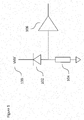
- Figure 1 a representation of a typical SPAD circuit is shown in Figure 1 .
- a voltage VHV 100 may be applied to the cathode of the SPAD 102.
- the anode is connected via a resistor 104 to ground, and to an input terminal of a comparator 106.
- a photon impinges on the detection region of the SPAD 102, a current is generated in the SPAD, and electrons collected at the anode of the SPAD.
- the current may be output to the comparator 106. If the current generated is above a threshold value, then an output pulse is produced by the comparator, indicating the detection of a photon.
- the circuit may also comprise reset circuitry (not shown) for resetting the SPAD ready for the next detection event.
- the anode may be discharged to ground via a resistor.
- the resistor may be replaced by a MOS device with a fixed gate bias. With either resistor or MOS with fixed bias, the SPAD is said to operate in active recharge mode.
- the SPAD circuit may also comprise a switch to a positive voltage on the anode, allowing the voltage across the SPAD to be reduced, thereby taking the SPAD out of the avalanche region.
- Figure 2 shows a representation of the current flowing through the SPAD as a function of the voltage applied across the SPAD. Initially, when there is a zero voltage difference, there is no current flowing, as denoted by the flat line region 200 in Figure 2 .
- VBD breakdown voltage
- the voltage applied As the voltage applied is made more negative, the voltage reaches a value which represents the minimum voltage required to cause an output pulse to be generated when a photon impinges upon the SPAD. This is the voltage difference required to accelerate the photo-generated carriers to sufficiently cause an avalanche within the SPAD. This is the minimum operation voltage 204, VHV 0 .
- the voltage difference may then be made more negative with respect to value 206, which represents an operating voltage of the SPAD which is of a sufficient magnitude so as to generate a current which is easily detectable by the SPAD and trigger an output pulse.
- the electric field applied may reach a value at which electron-hole pairs are generated spontaneously (i.e. without the device receiving a photon), resulting in dark current.
- a device comprises both a light emitter and a SPAD detector.
- the light emitter may for example be a vertical cavity surface emitting laser (VCSEL).
- VCSEL vertical cavity surface emitting laser
- Other embodiments may use other suitable light sources.
- light may be emitted by a VCSEL.
- a portion of the light may be reflected back to the SPAD detector. If the voltage applied to the SPAD is too low, then it is not possible to determine whether no light is being received is a result of the SPAD being improperly biased, or if there is no target within the field of view.
- FIG. 6 An example LIDAR system incorporating a reference light path is shown in Figure 6 .
- the system comprises a VCSEL 600, a reference SPAD 602 detector and a main SPAD detector 604.
- the VCSEL 600 may emit light across a wide angle, or field of view of the system, denoted by the dotted lines in Figure 6 . A portion of the light generated by the VCSEL 600 may be blocked by the device housing 610, while the remainder of the light is emitted.
- part of the light may be reflected back to the main SPAD detector 604, which receives the reflected light and counts the number of photons received.
- the number of counts, and timing information may be used to determine and locate objects within the field of view of the device.
- a solid partition 606 is located between the VCSEL 600 and the main SPAD detector 604 to ensure no stray light emitted from the VCSEL 600 is detected by the main SPAD detector 604 without it being reflected from the target 608.
- the reference light path 612 is formed by a portion of light emitted from the VCSEL 600 being reflected off the interior of the device housing 610, which is detected by the reference SPAD detector 602. Thus the reference light path 612 is engineered to always receive a portion of the light emitted by the VCSEL 600.
- the applied voltage may be gradually changed until a certain count threshold within a set integration period is achieved. This voltage is considered to be the minimum voltage required to cause the SPAD to emit an output pulse indicating a photon detection.
- the voltage applied to the main SPAD detector 604 may then be set to a value comprising the minimum threshold determined using the reference SPAD detector 602 plus an amount to enter into an assumed robust region of operation of the main SPAD detector 604.
- the time taken to perform the detection and calibration may not be insignificant - for example, it may be of the order of 1 ms, which is time in which data could be gathered.
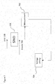
- FIG. 7 A representation of an apparatus according to some embodiments is shown in Figure 7 .
- the apparatus comprises a SPAD 102, measurement circuitry 702, and voltage setting circuitry 704.
- the SPAD 102 is supplied with a cathode voltage VHV 100 and an anode voltage 706.
- the anode of the SPAD 102 outputs a current to the measurement circuitry 702.
- the measurement circuitry 702 comprises circuitry suitable for measuring the current output from the SPAD 102.
- the measurement circuitry 702 is connected to the voltage setting circuitry 704.
- the voltage setting circuitry 704 comprises circuitry suitable for receiving an input from the measurement block 702, and controlling at least one of the cathode voltage VHV 100 and the anode voltage 706 applied to the SPAD based on the received input.
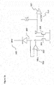
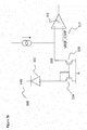
- FIG. 3a and 3b Some example circuits according to some embodiments are shown in Figures 3a and 3b . It should be understood that the circuits shown in Figure 3 are non-limiting example implementations of the apparatus described above with reference to Figure 7 . It should be understood that in some embodiments, different circuitry to that provided in Figure 3 may be used.
- the circuit shown in Figure 3a comprises a SPAD 102, first n-type FET transistor 304, a second n-type FET transistor 308, and an op-amp 302.
- the SPAD is biased by applying voltage VHV 100 to the SPAD cathode.
- the anode of the SPAD 102 is connected to source of the first transistor 304.
- the anode of the SPAD 102 is also connected to the non-inverting input terminal of op-amp 302.
- the inverting input terminal of the op-amp receives a biasing voltage VBG 306.
- the output of the op-amp 302 is connected to the gate of the first transistor 304 and the gate of the second transistor 308.
- the drain of the first transistor 304 and the second transistor 308 are connected together.
- the bias voltage VBG 306 determines the anode voltage of the SPAD 102.
- the arrangement of the circuit shown in Figure 3 results in the first transistor 304 and the second transistor 308 forming a current mirror.
- the current flowing through the SPAD 102 is input into the source of the first transistor 304 and is mirrored by the second transistor 308 and output at 310 to a current comparator 312.
- the current comparator 312 may compare the current 310 to a threshold value VREF_ICMP 314.
- At least one of the cathode voltage 100 and the bias voltage 306 may be dependent on the output of the current comparator 312.
- the measurement circuitry may comprise a current mirror.
- the current mirror may be connected to a current comparator.
- the current mirror may comprise a first transistor 304 and a second transistor 310, wherein a source terminal of the first transistor 304 is connected to an anode 102 of the single photon avalanche diode, and a drain terminal of the first transistor 304 is connected to a drain terminal of the second transistor 308.
- the drains of the first and second transistors may be held at a ground voltage.
- the source terminal of the second transistor 308 may be connected to a current comparator 310.
- the voltage setting circuitry may comprise an op-amp.
- the op-amp may receive a bias voltage VBG 306 at the inverting input terminal, and the output of the SPAD 102 at the non-inverting input terminal.
- the output of the op-amp may be connected to the gate of the first transistor 304 and the gate of the second transistor 308.
- the source of the first transistor may be connected to the anode of the SPAD 102.
- the bias voltage VBG 306 may be dependent on the output of the current comparator.
- the circuit shown in Figure 3b may be used.
- the circuit in Figure 3b is substantially the same as the circuit shown in Figure 3a , except that the op-amp 302 has been removed, and the gate of the first transistor 304 and the second transistor 306 may be connected to the output of the SPAD 102.
- the cathode voltage VHV 100 may be dependent on the output of the current comparator.
- n-type FETs in the circuits shown in Figure 3 and described above is only one such example. It would be understood by those skilled in the art that any other suitable transistor may be used. For example, a p-type FET may be used. It should be appreciated that alternatively or additionally, different types of transistor may be used such as bipolar transistors or MOSFETs.
- the circuit of Figure 3a may provide a more accurate control of the voltage across the SPAD 102.
- the circuit of Figure 3b may be smaller, and thus easier and cheaper to manufacture.
- the voltage VHV applied to the SPAD is fixed at a first value such that the voltage is well above the breakdown voltage VBD.
- the operation of setting the SPAD voltage to above VBD is shown in Figure 4 by step 400.
- the voltage applied across the SPAD may then be reduced.
- the operation of reducing the voltage applied across the SPAD is shown in Figure 4 by step 402.
- the current flowing through the SPAD may then be compared to a threshold value.
- the operation of comparing the current flowing through the SPAD to a threshold value is shown in Figure 4 by step 404.
- step 402 the voltage applied across the SPAD may be reduced, and the current flowing through the SPAD again determined and compared to the threshold value in step 404.
- the voltage applied across the SPAD may be increased by a fixed amount VEB.
- the subsequently applied voltage is determined to be the operating threshold voltage of the SPAD.
- the applied excess bias voltage VEB may be large enough to ensure that a current output from the SPAD exceeds a threshold current of the SPAD readout circuitry for all SPAD pixels.
- Increasing the excess bias voltage above this value may result in increasing the sensitivity of the SPAD - that is to say, an incident photon may be likely to trigger an avalanche in the SPAD when a large excess bias is applied.
- Increasing the excess bias may, however, also result in increased dark count rate (the dark count rate being outputs from the SPAD pixel which occur without the presence of a photon due to defects within the silicon).
- the applied excess bias voltage VEB may be determined by a trade-off between the achieved sensitivity and dark count rate. Additionally or alternatively, a further factor which may be considered is based on the ability to turn off the SPADs when they are not in operation.
- the SPAD may be disabled by pulling the anode voltage to a higher voltage.
- the anode voltage may be set by the supply voltage.
- the anode voltage being increased may cause the voltage across the SPAD to be lower than the breakdown voltage VBD, moving the SPAD out of its avalanche region.
- the applied excess bias voltage may be smaller than the voltage used to disable the SPAD to enable the SPAD to be disabled.
- the increase in the voltage may be dependent on the one or more other factors.
- the one or more other factors may be any other suitable factors such as temperature, operating conditions, application and/or the like. Employing an increased voltage may result in increased probability of detecting a photon at the expense of increased Dark Count Rate.
- the voltage VHV applied to the SPAD is fixed at a second value well below the breakdown voltage VBD.
- the operation of setting the voltage applied across the SPAD to above VBD is shown in Figure 5 by step 500.
- the voltage applied across the SPAD may then be increased.
- the operation of increasing the voltage applied across the SPAD is shown in Figure 5 by step 502.
- the current flowing through the SPAD may then be compared to a threshold value.
- the operation of comparing the current flowing through the SPAD to a threshold value is shown in Figure 5 by step 504.
- step 502 the voltage applied across the SPAD may be increased, and the current flowing through the SPAD again compared to the threshold value in step 504.
- the voltage applied across the SPAD may be increased by a fixed amount VEB.
- the subsequently applied voltage is determined to be the operating threshold voltage of the SPAD.
- the increase in the voltage may be dependent on the current voltage being used.
- the increase in the voltage may be dependent on the one or more other factors.
- the one or more other factors may be any other suitable factors such as temperature, operating conditions, application and/or the like.
- some embodiments may carry out steps 400 to 404 of Figure 4 and steps 500 to 504 of Figure 5 .
- the voltage which triggers the current to be below the threshold in Figure 4 and the voltage which triggers the current to be above the threshold in Figure 5 are both used to determine an operating bias voltage for the SPAD.
- Some embodiments may provide a method comprising determining a current flowing through a single photon avalanche diode, and controlling the voltage applied to the single photon avalanche diode in dependence on the determined current.
- determining the current flowing through the SPAD may comprise setting the voltage applied to the SPAD with respect to a threshold voltage, adjusting the voltage applied to the SPAD, and comparing the current flowing through the SPAD to a threshold current.
- setting the voltage applied to the SPAD with respect to a threshold voltage comprises setting the voltage applied to the SPAD above the threshold value. In some embodiments, setting the voltage applied to the SPAD with respect to a threshold voltage comprises setting the voltage applied to the SPAD below the threshold value.
- adjusting the voltage applied to the SPAD comprises reducing the voltage applied to the SPAD. In some embodiments, adjusting the voltage applied to the SPAD comprises increasing the voltage applied to the SPAD.
- the comparison is successful if the current flowing through the single photon avalanche diode is below a threshold current. In some embodiments, the comparison is successful if the current flowing through the single photon avalanche diode is above a threshold current.
- controlling the voltage applied to the SPAD in dependence on the determined current may comprise increasing the voltage applied to the SPAD by a set value in response to the comparison being successful.
- each SPAD may have its voltage individually controlled such as described previously.
- one or more SPADs may act as reference SPADs for the determining of a voltage. The determined voltage for these one or more SPADs may be used to control the voltage applied to one or more other SPADs. It should be appreciated that these so-called reference SPADs may be configured to be a detecting SPAD.
- the apparatus and method described above may be implemented in any device or apparatus which utilises single photon avalanche detectors.
- the apparatus and method described above may be implemented in automotive LIDAR, medical systems (fluorescence lifetime imaging microscopy for example), industrial ranging, light sensing and in communications. It should be understood that these non-limiting implementations are only exemplary, and the apparatus and method may be implemented in any manner of other light-detecting applications.
Landscapes
- Engineering & Computer Science (AREA)
- Physics & Mathematics (AREA)
- General Physics & Mathematics (AREA)
- Radar, Positioning & Navigation (AREA)
- Remote Sensing (AREA)
- Computer Networks & Wireless Communication (AREA)
- Electromagnetism (AREA)
- Nonlinear Science (AREA)
- Spectroscopy & Molecular Physics (AREA)
- Microelectronics & Electronic Packaging (AREA)
- Power Engineering (AREA)
- Automation & Control Theory (AREA)
- Light Receiving Elements (AREA)
- Photometry And Measurement Of Optical Pulse Characteristics (AREA)
Abstract
Description
- Some embodiments relate to a method and apparatus for controlling the voltage applied to a single photon avalanche diode.
- Single photon avalanche diodes (SPADs) are semiconductor devices capable of detecting light. A photon impinging on a detection region of a SPAD generates an electron and hole pair via the photoelectric effect. The SPAD is reverse-biased with a high voltage magnitude such that when the electron/hole carriers are generated, the electric field applied across the detection region causes the carriers to be accelerated to a relatively high velocity according to the strength and direction of the applied field. If the kinetic energy of the accelerated carriers is sufficient, additional carriers will be generated from the semiconductor lattice, which are in turn accelerated by the field, and may liberate further carriers in an exponentially increasing fashion. Thus, when a sufficiently high electric field is applied across the detection region, a single impinging photon may generate an avalanche of carriers, resulting in an output current 'pulse', where the current output is proportional to the number of photons detected.
- The minimum voltage required to cause an avalanche of carriers, and thus allow the device to operate as a SPAD, is known as the breakdown voltage. If the voltage applied across the SPAD is too low, i.e. below the breakdown voltage, then the device does not produce any output. However if the voltage applied across the SPAD is too high, then it is possible that the electric field generated may be sufficient to cause a carrier avalanche even when there are no photons impinging on the SPAD, resulting in a false output current. This false output is known as a "dark current".
- According to a first aspect, there is provided a method for controlling a voltage across a single photon avalanche diode, the method comprising: providing an output dependent on a current flowing through the single photon avalanche diode; and controlling the voltage applied across the single photon avalanche diode in dependence on the provided output.
- The provided output may comprise a current.
- The method may comprise determining when said provided output satisfies a condition and in response thereto to adjusting a current voltage applied across the single photon avalanche diode by a set voltage value.
- The steps of providing said output and controlling said voltage may be repeated until said output satisfies said condition.
- The method may comprise comparing said output to a threshold to control the voltage applied to said single photon avalanche diode.
- The method may comprise controlling an initial voltage across said single photon avalanche diode such that said initial voltage is one of greater and smaller than a voltage used in normal operation of said single photon avalanche diode; and adjusting said voltage in response to said provided output.
- The method may comprise adjusting an initial voltage such that said voltage is closer to a voltage used in normal operation of the single photon avalanche diode.
- Controlling the voltage applied across the single photon avalanche diode may comprise controlling at least one of: the cathode voltage applied to the single photon avalanche diode; and the anode voltage applied to the single photon avalanche diode.
- According to a second aspect, there is provided an apparatus for controlling a voltage applied across a single photon avalanche diode, the apparatus comprising: measurement circuitry configured to provide an output dependent on a current flowing through the single photon avalanche diode; and voltage setting circuitry configured to control the voltage applied across the single photon avalanche diode in dependence on the provided output.
- The provided output may comprise a current.
- The voltage setting circuitry may be configured to adjust a current voltage applied across the single photon avalanche diode by a set voltage in response to the provided output satisfying a condition.
- The voltage setting circuitry may be configured to control the voltage applied across said single photon avalanche diode in response to a comparison of said output to a threshold.
- The voltage setting circuitry may be configured to: control a voltage across said single photon avalanche diode such that said voltage is one of greater and smaller than a voltage user in normal operation of said single photon avalanche diode; and adjust said voltage in response to said provided output.
- The apparatus may comprise a current comparator configured to compare the provided output to a threshold current.
- The voltage setting circuitry may be configured to control at least one of the cathode voltage and the control voltage in dependence on the provided output.
- According to a third aspect, there is provided a device comprising an apparatus configured to provide an output dependent on a current flowing through a single photon avalanche diode; and control the voltage applied across the single photon avalanche diode in dependence on the provided output.
-
-
Figure 1 shows an example of a typical SPAD circuit; -
Figure 2 shows a graph of current flowing through a SPAD as a function of voltage bias applied to the SPAD; -
Figures 3a and3b show example circuits of some embodiments for measuring a current from the SPAD and controlling the voltage bias applied to a SPAD; -
Figures 4 and 5 show flow diagrams for the operation of setting the SPAD voltage according to some embodiments; -
Figure 6 shows a representation of an example LIDAR system incorporating a reference light path. - Some embodiments may provide circuitry for controlling the voltage applied across a SPAD. In order to aid understanding of some of the embodiments described herein, a representation of a typical SPAD circuit is shown in
Figure 1 . - In operation, a
voltage VHV 100 may be applied to the cathode of theSPAD 102. The anode is connected via aresistor 104 to ground, and to an input terminal of acomparator 106. When a photon impinges on the detection region of theSPAD 102, a current is generated in the SPAD, and electrons collected at the anode of the SPAD. The current may be output to thecomparator 106. If the current generated is above a threshold value, then an output pulse is produced by the comparator, indicating the detection of a photon. The circuit may also comprise reset circuitry (not shown) for resetting the SPAD ready for the next detection event. After a SPAD detection event, where the anode voltage increases to reduce the current flowing through the SPAD, the anode may be discharged to ground via a resistor. The resistor may be replaced by a MOS device with a fixed gate bias. With either resistor or MOS with fixed bias, the SPAD is said to operate in active recharge mode. - The SPAD circuit may also comprise a switch to a positive voltage on the anode, allowing the voltage across the SPAD to be reduced, thereby taking the SPAD out of the avalanche region.
- In order to better illustrate the operation of a SPAD, reference is now made to
Figure 2 . -
Figure 2 shows a representation of the current flowing through the SPAD as a function of the voltage applied across the SPAD. Initially, when there is a zero voltage difference, there is no current flowing, as denoted by theflat line region 200 inFigure 2 . - As the magnitude of the voltage difference between the cathode and the anode increases (i.e. the voltage is made more negative), the voltage difference reaches an
initial value 202 where the diode will start to conduct and current will begin to flow. This is known as the breakdown voltage, VBD. - As the voltage applied is made more negative, the voltage reaches a value which represents the minimum voltage required to cause an output pulse to be generated when a photon impinges upon the SPAD. This is the voltage difference required to accelerate the photo-generated carriers to sufficiently cause an avalanche within the SPAD. This is the
minimum operation voltage 204, VHV0. - The voltage difference may then be made more negative with respect to
value 206, which represents an operating voltage of the SPAD which is of a sufficient magnitude so as to generate a current which is easily detectable by the SPAD and trigger an output pulse. - However, if the voltage becomes too negative, i.e. the voltage magnitude becomes too high, then the electric field applied may reach a value at which electron-hole pairs are generated spontaneously (i.e. without the device receiving a photon), resulting in dark current.
- In some applications, such as optical communications or light detection and ranging (LIDAR), a device comprises both a light emitter and a SPAD detector. The light emitter may for example be a vertical cavity surface emitting laser (VCSEL). Other embodiments may use other suitable light sources.
- In the example of a LIDAR system, light may be emitted by a VCSEL. When the emitted light reaches a target within the field of view of the device, a portion of the light may be reflected back to the SPAD detector. If the voltage applied to the SPAD is too low, then it is not possible to determine whether no light is being received is a result of the SPAD being improperly biased, or if there is no target within the field of view.
- Equally, if the voltage difference applied to the SPAD is too high, it is not possible to determine if the current output is a result of a target being present, or if the current output is dark current generated by a high electric field.
- It has been proposed, in some devices, to provide a reference light path in the device. An example LIDAR system incorporating a reference light path is shown in
Figure 6 . The system comprises aVCSEL 600, areference SPAD 602 detector and a main SPAD detector 604. TheVCSEL 600 may emit light across a wide angle, or field of view of the system, denoted by the dotted lines inFigure 6 . A portion of the light generated by theVCSEL 600 may be blocked by thedevice housing 610, while the remainder of the light is emitted. - When a portion of the emitted light strikes a
target 608, part of the light may be reflected back to the main SPAD detector 604, which receives the reflected light and counts the number of photons received. The number of counts, and timing information may be used to determine and locate objects within the field of view of the device. - A
solid partition 606 is located between theVCSEL 600 and the main SPAD detector 604 to ensure no stray light emitted from theVCSEL 600 is detected by the main SPAD detector 604 without it being reflected from thetarget 608. - The
reference light path 612 is formed by a portion of light emitted from theVCSEL 600 being reflected off the interior of thedevice housing 610, which is detected by thereference SPAD detector 602. Thus thereference light path 612 is engineered to always receive a portion of the light emitted by theVCSEL 600. - With the
reference SPAD detector 602, the applied voltage may be gradually changed until a certain count threshold within a set integration period is achieved. This voltage is considered to be the minimum voltage required to cause the SPAD to emit an output pulse indicating a photon detection. - The voltage applied to the main SPAD detector 604 may then be set to a value comprising the minimum threshold determined using the
reference SPAD detector 602 plus an amount to enter into an assumed robust region of operation of the main SPAD detector 604. - This requires a reference light path to be built into the device, which requires additional space and results in an increased cost to manufacture. The time taken to perform the detection and calibration may not be insignificant - for example, it may be of the order of 1 ms, which is time in which data could be gathered.
- For some applications, it is desirable to control the voltage applied to a SPAD automatically and/or continuously, without the need for a reference light path.
- A representation of an apparatus according to some embodiments is shown in
Figure 7 . - In
Figure 7 , the apparatus comprises aSPAD 102,measurement circuitry 702, andvoltage setting circuitry 704. - The
SPAD 102 is supplied with acathode voltage VHV 100 and ananode voltage 706. The anode of theSPAD 102 outputs a current to themeasurement circuitry 702. Themeasurement circuitry 702 comprises circuitry suitable for measuring the current output from theSPAD 102. - The
measurement circuitry 702 is connected to thevoltage setting circuitry 704. Thevoltage setting circuitry 704 comprises circuitry suitable for receiving an input from themeasurement block 702, and controlling at least one of thecathode voltage VHV 100 and theanode voltage 706 applied to the SPAD based on the received input. - Some example circuits according to some embodiments are shown in
Figures 3a and3b . It should be understood that the circuits shown inFigure 3 are non-limiting example implementations of the apparatus described above with reference toFigure 7 . It should be understood that in some embodiments, different circuitry to that provided inFigure 3 may be used. - The circuit shown in
Figure 3a comprises aSPAD 102, first n-type FET transistor 304, a second n-type FET transistor 308, and an op-amp 302. The SPAD is biased by applyingvoltage VHV 100 to the SPAD cathode. The anode of theSPAD 102 is connected to source of thefirst transistor 304. The anode of theSPAD 102 is also connected to the non-inverting input terminal of op-amp 302. The inverting input terminal of the op-amp receives a biasing voltage VBG 306. The output of the op-amp 302 is connected to the gate of thefirst transistor 304 and the gate of thesecond transistor 308. The drain of thefirst transistor 304 and thesecond transistor 308 are connected together. - By varying the bias voltage VBG 306, the current passing through the first n-
type FET transistor 304 may be varied. Thus the bias voltage VBG 306 determines the anode voltage of theSPAD 102. - The arrangement of the circuit shown in
Figure 3 results in thefirst transistor 304 and thesecond transistor 308 forming a current mirror. Thus the current flowing through theSPAD 102, is input into the source of thefirst transistor 304 and is mirrored by thesecond transistor 308 and output at 310 to acurrent comparator 312. Thecurrent comparator 312 may compare the current 310 to athreshold value VREF_ICMP 314. - In some embodiments, at least one of the
cathode voltage 100 and the bias voltage 306 may be dependent on the output of thecurrent comparator 312. - That is to say, the measurement circuitry may comprise a current mirror. The current mirror may be connected to a current comparator. The current mirror may comprise a
first transistor 304 and asecond transistor 310, wherein a source terminal of thefirst transistor 304 is connected to ananode 102 of the single photon avalanche diode, and a drain terminal of thefirst transistor 304 is connected to a drain terminal of thesecond transistor 308. The drains of the first and second transistors may be held at a ground voltage. The source terminal of thesecond transistor 308 may be connected to acurrent comparator 310. - The voltage setting circuitry may comprise an op-amp. The op-amp may receive a bias voltage VBG 306 at the inverting input terminal, and the output of the
SPAD 102 at the non-inverting input terminal. The output of the op-amp may be connected to the gate of thefirst transistor 304 and the gate of thesecond transistor 308. The source of the first transistor may be connected to the anode of theSPAD 102. The bias voltage VBG 306 may be dependent on the output of the current comparator. - In some embodiments, the circuit shown in
Figure 3b may be used. The circuit inFigure 3b is substantially the same as the circuit shown inFigure 3a , except that the op-amp 302 has been removed, and the gate of thefirst transistor 304 and the second transistor 306 may be connected to the output of theSPAD 102. - In some embodiments, alternatively or additionally, the
cathode voltage VHV 100 may be dependent on the output of the current comparator. - It should be understood that the use of n-type FETs in the circuits shown in
Figure 3 and described above is only one such example. It would be understood by those skilled in the art that any other suitable transistor may be used. For example, a p-type FET may be used. It should be appreciated that alternatively or additionally, different types of transistor may be used such as bipolar transistors or MOSFETs. - With reference to
Figures 3a and3b , the circuit ofFigure 3a may provide a more accurate control of the voltage across theSPAD 102. The circuit ofFigure 3b may be smaller, and thus easier and cheaper to manufacture. - It should be appreciated that the examples shown in
Figure 3 are only two ways in which some embodiments may be implemented. Other embodiments may be implemented using different circuitry. - Some methods of some embodiments of controlling the voltage applied to a SPAD will now be described with reference to
Figures 4 and 5 . - According to some embodiments, the voltage VHV applied to the SPAD is fixed at a first value such that the voltage is well above the breakdown voltage VBD. The operation of setting the SPAD voltage to above VBD is shown in
Figure 4 bystep 400. - The voltage applied across the SPAD may then be reduced. The operation of reducing the voltage applied across the SPAD is shown in
Figure 4 bystep 402. - The current flowing through the SPAD may then be compared to a threshold value. The operation of comparing the current flowing through the SPAD to a threshold value is shown in
Figure 4 bystep 404. - If the current flowing through the SPAD is above the threshold value, the method repeats
step 402, where the voltage applied across the SPAD may be reduced, and the current flowing through the SPAD again determined and compared to the threshold value instep 404. - When the comparison in
step 404 results in the current flowing through the SPAD being below the threshold value, the voltage applied across the SPAD may be increased by a fixed amount VEB. The subsequently applied voltage is determined to be the operating threshold voltage of the SPAD. - The applied excess bias voltage VEB may be large enough to ensure that a current output from the SPAD exceeds a threshold current of the SPAD readout circuitry for all SPAD pixels. Increasing the excess bias voltage above this value may result in increasing the sensitivity of the SPAD - that is to say, an incident photon may be likely to trigger an avalanche in the SPAD when a large excess bias is applied. Increasing the excess bias may, however, also result in increased dark count rate (the dark count rate being outputs from the SPAD pixel which occur without the presence of a photon due to defects within the silicon).
- In some embodiments the applied excess bias voltage VEB may be determined by a trade-off between the achieved sensitivity and dark count rate. Additionally or alternatively, a further factor which may be considered is based on the ability to turn off the SPADs when they are not in operation.
- In some embodiments it may be possible to have some SPADs within an array enabled while others are disabled. For a SPAD configured with a high voltage VHV on the cathode and zero volts on the anode during normal operation, the SPAD may be disabled by pulling the anode voltage to a higher voltage. The anode voltage may be set by the supply voltage. The anode voltage being increased may cause the voltage across the SPAD to be lower than the breakdown voltage VBD, moving the SPAD out of its avalanche region. In some embodiments, the applied excess bias voltage may be smaller than the voltage used to disable the SPAD to enable the SPAD to be disabled.
- In some embodiments, the increase in the voltage may be dependent on the one or more other factors. The one or more other factors may be any other suitable factors such as temperature, operating conditions, application and/or the like. Employing an increased voltage may result in increased probability of detecting a photon at the expense of increased Dark Count Rate.
- The operation of increasing the voltage applied across the SPAD by VEB is shown in
Figure 4 bystep 406. - According to another embodiment, the voltage VHV applied to the SPAD is fixed at a second value well below the breakdown voltage VBD. The operation of setting the voltage applied across the SPAD to above VBD is shown in
Figure 5 bystep 500. - The voltage applied across the SPAD may then be increased. The operation of increasing the voltage applied across the SPAD is shown in
Figure 5 bystep 502. - The current flowing through the SPAD may then be compared to a threshold value. The operation of comparing the current flowing through the SPAD to a threshold value is shown in
Figure 5 bystep 504. - If the current flowing through the SPAD is below the threshold value, the method repeats
step 502, where the voltage applied across the SPAD may be increased, and the current flowing through the SPAD again compared to the threshold value instep 504. - When the comparison in
step 504 results in the current flowing through the SPAD being above the threshold value, the voltage applied across the SPAD may be increased by a fixed amount VEB. The subsequently applied voltage is determined to be the operating threshold voltage of the SPAD. - The operation of increasing the voltage applied across the SPAD by VEB is shown in
Figure 5 bystep 506. - In some embodiments, the increase in the voltage may be dependent on the current voltage being used.
- In some embodiments, the increase in the voltage may be dependent on the one or more other factors. The one or more other factors may be any other suitable factors such as temperature, operating conditions, application and/or the like.
- In one modification, some embodiments may carry out
steps 400 to 404 ofFigure 4 andsteps 500 to 504 ofFigure 5 . The voltage which triggers the current to be below the threshold inFigure 4 and the voltage which triggers the current to be above the threshold inFigure 5 are both used to determine an operating bias voltage for the SPAD. - Some embodiments may provide a method comprising determining a current flowing through a single photon avalanche diode, and controlling the voltage applied to the single photon avalanche diode in dependence on the determined current.
- In some embodiments, determining the current flowing through the SPAD may comprise setting the voltage applied to the SPAD with respect to a threshold voltage, adjusting the voltage applied to the SPAD, and comparing the current flowing through the SPAD to a threshold current.
- In some embodiments, setting the voltage applied to the SPAD with respect to a threshold voltage comprises setting the voltage applied to the SPAD above the threshold value. In some embodiments, setting the voltage applied to the SPAD with respect to a threshold voltage comprises setting the voltage applied to the SPAD below the threshold value.
- In some embodiments, adjusting the voltage applied to the SPAD comprises reducing the voltage applied to the SPAD. In some embodiments, adjusting the voltage applied to the SPAD comprises increasing the voltage applied to the SPAD.
- In some embodiments, the comparison is successful if the current flowing through the single photon avalanche diode is below a threshold current. In some embodiments, the comparison is successful if the current flowing through the single photon avalanche diode is above a threshold current.
- In some embodiments, controlling the voltage applied to the SPAD in dependence on the determined current may comprise increasing the voltage applied to the SPAD by a set value in response to the comparison being successful.
- In some embodiments there may be a single SPAD. In other embodiments, there may be an array of SPADs. Where there is more than one SPAD, each SPAD may have its voltage individually controlled such as described previously. In some embodiments, where there is more than one SPAD, one or more SPADs may act as reference SPADs for the determining of a voltage. The determined voltage for these one or more SPADs may be used to control the voltage applied to one or more other SPADs. It should be appreciated that these so-called reference SPADs may be configured to be a detecting SPAD.
- The apparatus and method described above may be implemented in any device or apparatus which utilises single photon avalanche detectors. For example, the apparatus and method described above may be implemented in automotive LIDAR, medical systems (fluorescence lifetime imaging microscopy for example), industrial ranging, light sensing and in communications. It should be understood that these non-limiting implementations are only exemplary, and the apparatus and method may be implemented in any manner of other light-detecting applications.
- It should be appreciated that the above described arrangements may be implemented at least partially by an integrated circuit, a chip set, one or more dies packaged together or in different packages, discrete circuitry or any combination of these options.
- Various embodiments with different variations have been described here above. It should be noted that those skilled in the art may combine various elements of these various embodiments and variations.
- Such alterations, modifications, and improvements are intended to be part of this disclosure, and are intended to be within the scope of the present invention. Accordingly, the foregoing description is by way of example only and is not intended to be limiting. The present invention is limited only as defined in the following claims and the equivalents thereto.
Claims (15)
- A method for controlling a voltage across a single photon avalanche diode, the method comprising:providing an output dependent on a current flowing through the single photon avalanche diode; andcontrolling the voltage applied across the single photon avalanche diode in dependence on the provided output.
- The method of claim 1, wherein said provided output comprises a current.
- The method of claim 1 or 2, comprising determining when said provided output satisfies a condition and in response thereto to adjusting a current voltage applied across the single photon avalanche diode by a set voltage value.
- The method as claimed in claim 3, wherein said steps of providing said output and controlling said voltage are repeated until said output satisfies said condition.
- The method of any preceding claim, wherein said method further comprises comparing said output to a threshold to control the voltage applied across said single photon avalanche diode.
- The method of any preceding claim, comprising:controlling an initial voltage across said single photon avalanche diode such that said initial voltage is one of greater and smaller than a voltage used in normal operation of said single photon avalanche diode; andadjusting said voltage in response to said provided output.
- The method as claimed in claim 5, comprising adjusting an initial voltage such that said voltage is closer to a voltage used in normal operation of the single photon avalanche diode.
- The method of any preceding claim, wherein controlling the voltage applied to the single photon avalanche diode comprises controlling at least one of:the cathode voltage applied to the single photon avalanche diode; andthe anode voltage applied to the single photon avalanche diode.
- An apparatus for controlling a voltage applied across a single photon avalanche diode, the apparatus comprising:measurement circuitry configured to provide an output dependent on a current flowing through the single photon avalanche diode; andvoltage setting circuitry configured to control the voltage applied across the single photon avalanche diode in dependence on the provided output.
- The apparatus of claim 9, wherein said provided output comprises a current.
- The apparatus of any of claims 9 and 10, wherein the voltage setting circuitry is configured to adjust a current voltage applied across the single photon avalanche diode by a set voltage in response to the provided output satisfying a condition.
- The apparatus of any of claims 9 to 11, wherein the voltage setting circuitry is configured to control the voltage applied across said single photon avalanche diode in response to a comparison of said output to a threshold.
- The apparatus of any of claims 9 to 12, wherein the voltage setting circuitry is configured to:control a voltage across said single photon avalanche diode such that said voltage is one of greater and smaller than a voltage user in normal operation of said single photon avalanche diode; andadjust said voltage in response to said provided output.
- The apparatus of any of claims 9 to 13, comprising a current comparator configured to compare the provided output to a threshold current.
- The apparatus of any of claims 9 to 14, wherein the voltage setting circuitry is configured to control at least one of the cathode voltage and the control voltage in dependence on the provided output.
Priority Applications (4)
| Application Number | Priority Date | Filing Date | Title |
|---|---|---|---|
| EP18209521.6A EP3660473B1 (en) | 2018-11-30 | 2018-11-30 | Apparatus and method for controlling the voltage applied to a single photon avalanche photodiode (spad) |
| US16/681,569 US11274964B2 (en) | 2018-11-30 | 2019-11-12 | Apparatus and method for controlling the voltage applied to a SPAD |
| CN201922103202.XU CN211044058U (en) | 2018-11-30 | 2019-11-29 | Apparatus and electronics for controlling voltage applied across a single-photon avalanche diode |
| CN201911199598.0A CN111258367A (en) | 2018-11-30 | 2019-11-29 | Apparatus and method for controlling voltage applied to SPAD |
Applications Claiming Priority (1)
| Application Number | Priority Date | Filing Date | Title |
|---|---|---|---|
| EP18209521.6A EP3660473B1 (en) | 2018-11-30 | 2018-11-30 | Apparatus and method for controlling the voltage applied to a single photon avalanche photodiode (spad) |
Publications (2)
| Publication Number | Publication Date |
|---|---|
| EP3660473A1 true EP3660473A1 (en) | 2020-06-03 |
| EP3660473B1 EP3660473B1 (en) | 2024-09-18 |
Family
ID=64564678
Family Applications (1)
| Application Number | Title | Priority Date | Filing Date |
|---|---|---|---|
| EP18209521.6A Active EP3660473B1 (en) | 2018-11-30 | 2018-11-30 | Apparatus and method for controlling the voltage applied to a single photon avalanche photodiode (spad) |
Country Status (3)
| Country | Link |
|---|---|
| US (1) | US11274964B2 (en) |
| EP (1) | EP3660473B1 (en) |
| CN (2) | CN211044058U (en) |
Families Citing this family (6)
| Publication number | Priority date | Publication date | Assignee | Title |
|---|---|---|---|---|
| EP3660473B1 (en) | 2018-11-30 | 2024-09-18 | STMicroelectronics (Research & Development) Limited | Apparatus and method for controlling the voltage applied to a single photon avalanche photodiode (spad) |
| US11579290B2 (en) * | 2019-06-05 | 2023-02-14 | Stmicroelectronics (Research & Development) Limited | LIDAR system utilizing multiple networked LIDAR integrated circuits |
| US11728621B2 (en) | 2019-06-05 | 2023-08-15 | Stmicroelectronics (Research & Development) Limited | Voltage controlled steered VCSEL driver |
| US11131781B2 (en) * | 2019-09-20 | 2021-09-28 | Waymo Llc | Programmable SiPM arrays |
| US11221253B2 (en) * | 2020-01-21 | 2022-01-11 | Semiconductor Components Industries, Llc | System with a SPAD-based semiconductor device having dark pixels for monitoring sensor parameters |
| CN115963374A (en) * | 2022-10-08 | 2023-04-14 | 深圳市灵明光子科技有限公司 | Self-adaptive adjusting circuit and laser ranging chip |
Citations (3)
| Publication number | Priority date | Publication date | Assignee | Title |
|---|---|---|---|---|
| US20080017785A1 (en) * | 2006-07-19 | 2008-01-24 | Raytheon Company | Automatic avalanche photodiode bias setting system based on unity-gain noise measurement |
| US20130009266A1 (en) * | 2011-07-04 | 2013-01-10 | Hamamatsu Photonics K.K. | Photodiode array, method for determining reference voltage, and method for determining recommended operating voltage |
| JP2018179732A (en) * | 2017-04-12 | 2018-11-15 | 株式会社デンソー | Light detector |
Family Cites Families (16)
| Publication number | Priority date | Publication date | Assignee | Title |
|---|---|---|---|---|
| EP0924823A1 (en) * | 1997-12-17 | 1999-06-23 | Hewlett-Packard Company | Driver circuit for a solid state optical emitter device |
| US7087882B1 (en) * | 2002-10-31 | 2006-08-08 | Finisar Corporation | Controlling the dynamic range of an avalanche photodiode |
| JP4670496B2 (en) * | 2005-06-14 | 2011-04-13 | 住友電気工業株式会社 | Optical receiver |
| CN2921917Y (en) * | 2006-06-16 | 2007-07-11 | 普诚科技股份有限公司 | Electric current mirror and illuminating device using the same current mirror |
| CN101464700A (en) * | 2007-12-18 | 2009-06-24 | 原景科技股份有限公司 | Current mirror circuit |
| CN101562323B (en) * | 2008-12-30 | 2012-04-18 | 天津南大强芯半导体芯片设计有限公司 | Short-circuit protection circuit |
| JP5580608B2 (en) * | 2009-02-23 | 2014-08-27 | セイコーインスツル株式会社 | Voltage regulator |
| CN101762736A (en) * | 2009-11-09 | 2010-06-30 | 天津南大强芯半导体芯片设计有限公司 | Image current detecting circuit |
| JP5691158B2 (en) * | 2009-11-13 | 2015-04-01 | ミツミ電機株式会社 | Output current detection circuit and transmission circuit |
| JP2011252716A (en) * | 2010-05-31 | 2011-12-15 | Sumitomo Electric Device Innovations Inc | Light intensity measurement method |
| CN102360236B (en) * | 2011-07-07 | 2013-12-18 | 上海如韵电子有限公司 | High-voltage end current detection circuit |
| CN102591392B (en) * | 2012-02-01 | 2013-11-27 | 深圳创维-Rgb电子有限公司 | A low dropout linear regulator and chip |
| CN102735351B (en) | 2012-06-27 | 2014-05-07 | 华南师范大学 | Single-photon detector circuit and detection method thereof |
| EP3540390B1 (en) * | 2016-11-11 | 2021-09-22 | Hamamatsu Photonics K.K. | Light detection device |
| JP6924085B2 (en) * | 2017-06-27 | 2021-08-25 | キヤノン株式会社 | Photodetector and imaging system |
| EP3660473B1 (en) | 2018-11-30 | 2024-09-18 | STMicroelectronics (Research & Development) Limited | Apparatus and method for controlling the voltage applied to a single photon avalanche photodiode (spad) |
-
2018
- 2018-11-30 EP EP18209521.6A patent/EP3660473B1/en active Active
-
2019
- 2019-11-12 US US16/681,569 patent/US11274964B2/en active Active
- 2019-11-29 CN CN201922103202.XU patent/CN211044058U/en active Active
- 2019-11-29 CN CN201911199598.0A patent/CN111258367A/en active Pending
Patent Citations (3)
| Publication number | Priority date | Publication date | Assignee | Title |
|---|---|---|---|---|
| US20080017785A1 (en) * | 2006-07-19 | 2008-01-24 | Raytheon Company | Automatic avalanche photodiode bias setting system based on unity-gain noise measurement |
| US20130009266A1 (en) * | 2011-07-04 | 2013-01-10 | Hamamatsu Photonics K.K. | Photodiode array, method for determining reference voltage, and method for determining recommended operating voltage |
| JP2018179732A (en) * | 2017-04-12 | 2018-11-15 | 株式会社デンソー | Light detector |
Also Published As
| Publication number | Publication date |
|---|---|
| CN111258367A (en) | 2020-06-09 |
| US20200173846A1 (en) | 2020-06-04 |
| EP3660473B1 (en) | 2024-09-18 |
| CN211044058U (en) | 2020-07-17 |
| US11274964B2 (en) | 2022-03-15 |
Similar Documents
| Publication | Publication Date | Title |
|---|---|---|
| US11274964B2 (en) | Apparatus and method for controlling the voltage applied to a SPAD | |
| US10585174B2 (en) | LiDAR readout circuit | |
| CN113224090A (en) | Imaging system | |
| US9190552B2 (en) | Method and device for adjusting the bias voltage of a SPAD photodiode | |
| JP6225411B2 (en) | Optical distance measuring device | |
| US20150364635A1 (en) | Single photon counting | |
| US11913831B2 (en) | Optical sensor and method of operating an optical sensor | |
| CN112098973B (en) | Light receiving device for laser radar and dynamic adjustment method of light receiving device | |
| US20140103196A1 (en) | Light detector | |
| US11614519B2 (en) | Arrangements of light-receiving elements with different sensitivities and methods for receiving light signals | |
| CN113218504A (en) | Imaging system with single photon avalanche diode and ambient light level detection | |
| US12007481B2 (en) | Sensor and distance measuring device | |
| EP3709053A1 (en) | Sensor and distance measuring device | |
| US20220082668A1 (en) | Light detector and distance measurement device | |
| US20160282451A1 (en) | Lidar system | |
| JP7434128B2 (en) | distance measuring device | |
| US12326503B2 (en) | Distance measuring apparatus | |
| US11139326B2 (en) | Photodetector, photodetection device, laser imaging detection and ranging apparatus | |
| JP6847878B2 (en) | Photodetector, photodetector and lidar device | |
| CN112154546A (en) | Photodetector and optical distance measuring device using the same | |
| US20260039977A1 (en) | Image sensing device and method of operating the same | |
| JP5273606B2 (en) | Optical feedback photodetector | |
| US20220163642A1 (en) | Current generation circuit and ranging system | |
| US12439182B2 (en) | Photodetector, electronic device, and method of photodetection | |
| US20240192328A1 (en) | Photodetection device and distance measurement device |
Legal Events
| Date | Code | Title | Description |
|---|---|---|---|
| PUAI | Public reference made under article 153(3) epc to a published international application that has entered the european phase |
Free format text: ORIGINAL CODE: 0009012 |
|
| STAA | Information on the status of an ep patent application or granted ep patent |
Free format text: STATUS: THE APPLICATION HAS BEEN PUBLISHED |
|
| AK | Designated contracting states |
Kind code of ref document: A1 Designated state(s): AL AT BE BG CH CY CZ DE DK EE ES FI FR GB GR HR HU IE IS IT LI LT LU LV MC MK MT NL NO PL PT RO RS SE SI SK SM TR |
|
| AX | Request for extension of the european patent |
Extension state: BA ME |
|
| STAA | Information on the status of an ep patent application or granted ep patent |
Free format text: STATUS: REQUEST FOR EXAMINATION WAS MADE |
|
| 17P | Request for examination filed |
Effective date: 20201127 |
|
| RBV | Designated contracting states (corrected) |
Designated state(s): AL AT BE BG CH CY CZ DE DK EE ES FI FR GB GR HR HU IE IS IT LI LT LU LV MC MK MT NL NO PL PT RO RS SE SI SK SM TR |
|
| STAA | Information on the status of an ep patent application or granted ep patent |
Free format text: STATUS: EXAMINATION IS IN PROGRESS |
|
| 17Q | First examination report despatched |
Effective date: 20221124 |
|
| GRAP | Despatch of communication of intention to grant a patent |
Free format text: ORIGINAL CODE: EPIDOSNIGR1 |
|
| STAA | Information on the status of an ep patent application or granted ep patent |
Free format text: STATUS: GRANT OF PATENT IS INTENDED |
|
| RIC1 | Information provided on ipc code assigned before grant |
Ipc: G01S 17/08 20060101ALI20240321BHEP Ipc: G01S 7/497 20060101ALI20240321BHEP Ipc: G01S 7/4913 20200101ALI20240321BHEP Ipc: G01S 7/4861 20200101ALI20240321BHEP Ipc: G01S 7/481 20060101ALI20240321BHEP Ipc: G01J 1/44 20060101AFI20240321BHEP |
|
| INTG | Intention to grant announced |
Effective date: 20240415 |
|
| GRAS | Grant fee paid |
Free format text: ORIGINAL CODE: EPIDOSNIGR3 |
|
| GRAA | (expected) grant |
Free format text: ORIGINAL CODE: 0009210 |
|
| STAA | Information on the status of an ep patent application or granted ep patent |
Free format text: STATUS: THE PATENT HAS BEEN GRANTED |
|
| AK | Designated contracting states |
Kind code of ref document: B1 Designated state(s): AL AT BE BG CH CY CZ DE DK EE ES FI FR GB GR HR HU IE IS IT LI LT LU LV MC MK MT NL NO PL PT RO RS SE SI SK SM TR |
|
| REG | Reference to a national code |
Ref country code: GB Ref legal event code: FG4D |
|
| REG | Reference to a national code |
Ref country code: CH Ref legal event code: EP |
|
| REG | Reference to a national code |
Ref country code: IE Ref legal event code: FG4D |
|
| REG | Reference to a national code |
Ref country code: DE Ref legal event code: R096 Ref document number: 602018074451 Country of ref document: DE |
|
| REG | Reference to a national code |
Ref country code: LT Ref legal event code: MG9D |
|
| PG25 | Lapsed in a contracting state [announced via postgrant information from national office to epo] |
Ref country code: NO Free format text: LAPSE BECAUSE OF FAILURE TO SUBMIT A TRANSLATION OF THE DESCRIPTION OR TO PAY THE FEE WITHIN THE PRESCRIBED TIME-LIMIT Effective date: 20241218 |
|
| PG25 | Lapsed in a contracting state [announced via postgrant information from national office to epo] |
Ref country code: GR Free format text: LAPSE BECAUSE OF FAILURE TO SUBMIT A TRANSLATION OF THE DESCRIPTION OR TO PAY THE FEE WITHIN THE PRESCRIBED TIME-LIMIT Effective date: 20241219 Ref country code: FI Free format text: LAPSE BECAUSE OF FAILURE TO SUBMIT A TRANSLATION OF THE DESCRIPTION OR TO PAY THE FEE WITHIN THE PRESCRIBED TIME-LIMIT Effective date: 20240918 |
|
| PG25 | Lapsed in a contracting state [announced via postgrant information from national office to epo] |
Ref country code: BG Free format text: LAPSE BECAUSE OF FAILURE TO SUBMIT A TRANSLATION OF THE DESCRIPTION OR TO PAY THE FEE WITHIN THE PRESCRIBED TIME-LIMIT Effective date: 20240918 |
|
| PG25 | Lapsed in a contracting state [announced via postgrant information from national office to epo] |
Ref country code: LV Free format text: LAPSE BECAUSE OF FAILURE TO SUBMIT A TRANSLATION OF THE DESCRIPTION OR TO PAY THE FEE WITHIN THE PRESCRIBED TIME-LIMIT Effective date: 20240918 |
|
| PG25 | Lapsed in a contracting state [announced via postgrant information from national office to epo] |
Ref country code: HR Free format text: LAPSE BECAUSE OF FAILURE TO SUBMIT A TRANSLATION OF THE DESCRIPTION OR TO PAY THE FEE WITHIN THE PRESCRIBED TIME-LIMIT Effective date: 20240918 |
|
| REG | Reference to a national code |
Ref country code: NL Ref legal event code: MP Effective date: 20240918 |
|
| PG25 | Lapsed in a contracting state [announced via postgrant information from national office to epo] |
Ref country code: RS Free format text: LAPSE BECAUSE OF FAILURE TO SUBMIT A TRANSLATION OF THE DESCRIPTION OR TO PAY THE FEE WITHIN THE PRESCRIBED TIME-LIMIT Effective date: 20241218 |
|
| PG25 | Lapsed in a contracting state [announced via postgrant information from national office to epo] |
Ref country code: RS Free format text: LAPSE BECAUSE OF FAILURE TO SUBMIT A TRANSLATION OF THE DESCRIPTION OR TO PAY THE FEE WITHIN THE PRESCRIBED TIME-LIMIT Effective date: 20241218 Ref country code: NO Free format text: LAPSE BECAUSE OF FAILURE TO SUBMIT A TRANSLATION OF THE DESCRIPTION OR TO PAY THE FEE WITHIN THE PRESCRIBED TIME-LIMIT Effective date: 20241218 Ref country code: LV Free format text: LAPSE BECAUSE OF FAILURE TO SUBMIT A TRANSLATION OF THE DESCRIPTION OR TO PAY THE FEE WITHIN THE PRESCRIBED TIME-LIMIT Effective date: 20240918 Ref country code: HR Free format text: LAPSE BECAUSE OF FAILURE TO SUBMIT A TRANSLATION OF THE DESCRIPTION OR TO PAY THE FEE WITHIN THE PRESCRIBED TIME-LIMIT Effective date: 20240918 Ref country code: GR Free format text: LAPSE BECAUSE OF FAILURE TO SUBMIT A TRANSLATION OF THE DESCRIPTION OR TO PAY THE FEE WITHIN THE PRESCRIBED TIME-LIMIT Effective date: 20241219 Ref country code: FI Free format text: LAPSE BECAUSE OF FAILURE TO SUBMIT A TRANSLATION OF THE DESCRIPTION OR TO PAY THE FEE WITHIN THE PRESCRIBED TIME-LIMIT Effective date: 20240918 Ref country code: BG Free format text: LAPSE BECAUSE OF FAILURE TO SUBMIT A TRANSLATION OF THE DESCRIPTION OR TO PAY THE FEE WITHIN THE PRESCRIBED TIME-LIMIT Effective date: 20240918 |
|
| REG | Reference to a national code |
Ref country code: AT Ref legal event code: MK05 Ref document number: 1725070 Country of ref document: AT Kind code of ref document: T Effective date: 20240918 |
|
| PG25 | Lapsed in a contracting state [announced via postgrant information from national office to epo] |
Ref country code: NL Free format text: LAPSE BECAUSE OF FAILURE TO SUBMIT A TRANSLATION OF THE DESCRIPTION OR TO PAY THE FEE WITHIN THE PRESCRIBED TIME-LIMIT Effective date: 20240918 |
|
| PG25 | Lapsed in a contracting state [announced via postgrant information from national office to epo] |
Ref country code: PT Free format text: LAPSE BECAUSE OF FAILURE TO SUBMIT A TRANSLATION OF THE DESCRIPTION OR TO PAY THE FEE WITHIN THE PRESCRIBED TIME-LIMIT Effective date: 20250120 Ref country code: IS Free format text: LAPSE BECAUSE OF FAILURE TO SUBMIT A TRANSLATION OF THE DESCRIPTION OR TO PAY THE FEE WITHIN THE PRESCRIBED TIME-LIMIT Effective date: 20250118 |
|
| PG25 | Lapsed in a contracting state [announced via postgrant information from national office to epo] |
Ref country code: RO Free format text: LAPSE BECAUSE OF FAILURE TO SUBMIT A TRANSLATION OF THE DESCRIPTION OR TO PAY THE FEE WITHIN THE PRESCRIBED TIME-LIMIT Effective date: 20240918 Ref country code: SM Free format text: LAPSE BECAUSE OF FAILURE TO SUBMIT A TRANSLATION OF THE DESCRIPTION OR TO PAY THE FEE WITHIN THE PRESCRIBED TIME-LIMIT Effective date: 20240918 |
|
| PG25 | Lapsed in a contracting state [announced via postgrant information from national office to epo] |
Ref country code: ES Free format text: LAPSE BECAUSE OF FAILURE TO SUBMIT A TRANSLATION OF THE DESCRIPTION OR TO PAY THE FEE WITHIN THE PRESCRIBED TIME-LIMIT Effective date: 20240918 |
|
| PG25 | Lapsed in a contracting state [announced via postgrant information from national office to epo] |
Ref country code: AT Free format text: LAPSE BECAUSE OF FAILURE TO SUBMIT A TRANSLATION OF THE DESCRIPTION OR TO PAY THE FEE WITHIN THE PRESCRIBED TIME-LIMIT Effective date: 20240918 Ref country code: EE Free format text: LAPSE BECAUSE OF FAILURE TO SUBMIT A TRANSLATION OF THE DESCRIPTION OR TO PAY THE FEE WITHIN THE PRESCRIBED TIME-LIMIT Effective date: 20240918 |
|
| PG25 | Lapsed in a contracting state [announced via postgrant information from national office to epo] |
Ref country code: CZ Free format text: LAPSE BECAUSE OF FAILURE TO SUBMIT A TRANSLATION OF THE DESCRIPTION OR TO PAY THE FEE WITHIN THE PRESCRIBED TIME-LIMIT Effective date: 20240918 Ref country code: PL Free format text: LAPSE BECAUSE OF FAILURE TO SUBMIT A TRANSLATION OF THE DESCRIPTION OR TO PAY THE FEE WITHIN THE PRESCRIBED TIME-LIMIT Effective date: 20240918 |
|
| PG25 | Lapsed in a contracting state [announced via postgrant information from national office to epo] |
Ref country code: SK Free format text: LAPSE BECAUSE OF FAILURE TO SUBMIT A TRANSLATION OF THE DESCRIPTION OR TO PAY THE FEE WITHIN THE PRESCRIBED TIME-LIMIT Effective date: 20240918 Ref country code: IT Free format text: LAPSE BECAUSE OF FAILURE TO SUBMIT A TRANSLATION OF THE DESCRIPTION OR TO PAY THE FEE WITHIN THE PRESCRIBED TIME-LIMIT Effective date: 20240918 |
|
| REG | Reference to a national code |
Ref country code: DE Ref legal event code: R097 Ref document number: 602018074451 Country of ref document: DE |
|
| REG | Reference to a national code |
Ref country code: CH Ref legal event code: PL |
|
| PG25 | Lapsed in a contracting state [announced via postgrant information from national office to epo] |
Ref country code: MC Free format text: LAPSE BECAUSE OF FAILURE TO SUBMIT A TRANSLATION OF THE DESCRIPTION OR TO PAY THE FEE WITHIN THE PRESCRIBED TIME-LIMIT Effective date: 20240918 |
|
| PG25 | Lapsed in a contracting state [announced via postgrant information from national office to epo] |
Ref country code: DK Free format text: LAPSE BECAUSE OF FAILURE TO SUBMIT A TRANSLATION OF THE DESCRIPTION OR TO PAY THE FEE WITHIN THE PRESCRIBED TIME-LIMIT Effective date: 20240918 |
|
| PG25 | Lapsed in a contracting state [announced via postgrant information from national office to epo] |
Ref country code: LU Free format text: LAPSE BECAUSE OF NON-PAYMENT OF DUE FEES Effective date: 20241130 |
|
| REG | Reference to a national code |
Ref country code: CH Ref legal event code: PL |
|
| PG25 | Lapsed in a contracting state [announced via postgrant information from national office to epo] |
Ref country code: CH Free format text: LAPSE BECAUSE OF NON-PAYMENT OF DUE FEES Effective date: 20241130 |
|
| PLBE | No opposition filed within time limit |
Free format text: ORIGINAL CODE: 0009261 |
|
| STAA | Information on the status of an ep patent application or granted ep patent |
Free format text: STATUS: NO OPPOSITION FILED WITHIN TIME LIMIT |
|
| 26N | No opposition filed |
Effective date: 20250619 |
|
| GBPC | Gb: european patent ceased through non-payment of renewal fee |
Effective date: 20241218 |
|
| REG | Reference to a national code |
Ref country code: BE Ref legal event code: MM Effective date: 20241130 |
|
| PG25 | Lapsed in a contracting state [announced via postgrant information from national office to epo] |
Ref country code: SE Free format text: LAPSE BECAUSE OF FAILURE TO SUBMIT A TRANSLATION OF THE DESCRIPTION OR TO PAY THE FEE WITHIN THE PRESCRIBED TIME-LIMIT Effective date: 20240918 |
|
| PG25 | Lapsed in a contracting state [announced via postgrant information from national office to epo] |
Ref country code: GB Free format text: LAPSE BECAUSE OF NON-PAYMENT OF DUE FEES Effective date: 20241218 Ref country code: BE Free format text: LAPSE BECAUSE OF NON-PAYMENT OF DUE FEES Effective date: 20241130 |
|
| PG25 | Lapsed in a contracting state [announced via postgrant information from national office to epo] |
Ref country code: FR Free format text: LAPSE BECAUSE OF NON-PAYMENT OF DUE FEES Effective date: 20241130 |
|
| PG25 | Lapsed in a contracting state [announced via postgrant information from national office to epo] |
Ref country code: IE Free format text: LAPSE BECAUSE OF NON-PAYMENT OF DUE FEES Effective date: 20241130 |
|
| REG | Reference to a national code |
Ref country code: DE Ref legal event code: R082 Ref document number: 602018074451 Country of ref document: DE Representative=s name: WESTPHAL, MUSSGNUG & PARTNER PATENTANWAELTE MI, DE |
|
| PGFP | Annual fee paid to national office [announced via postgrant information from national office to epo] |
Ref country code: DE Payment date: 20251022 Year of fee payment: 8 |
|
| PG25 | Lapsed in a contracting state [announced via postgrant information from national office to epo] |
Ref country code: CY Free format text: LAPSE BECAUSE OF FAILURE TO SUBMIT A TRANSLATION OF THE DESCRIPTION OR TO PAY THE FEE WITHIN THE PRESCRIBED TIME-LIMIT; INVALID AB INITIO Effective date: 20181130 |