EP3659507A1 - Radiation image capturing device - Google Patents
Radiation image capturing device Download PDFInfo
- Publication number
- EP3659507A1 EP3659507A1 EP18838805.2A EP18838805A EP3659507A1 EP 3659507 A1 EP3659507 A1 EP 3659507A1 EP 18838805 A EP18838805 A EP 18838805A EP 3659507 A1 EP3659507 A1 EP 3659507A1
- Authority
- EP
- European Patent Office
- Prior art keywords
- radiation
- sample
- signal
- hold
- irradiation
- Prior art date
- Legal status (The legal status is an assumption and is not a legal conclusion. Google has not performed a legal analysis and makes no representation as to the accuracy of the status listed.)
- Granted
Links
Images






Classifications
-
- G—PHYSICS
- G01—MEASURING; TESTING
- G01T—MEASUREMENT OF NUCLEAR OR X-RADIATION
- G01T1/00—Measuring X-radiation, gamma radiation, corpuscular radiation, or cosmic radiation
- G01T1/16—Measuring radiation intensity
- G01T1/17—Circuit arrangements not adapted to a particular type of detector
-
- H—ELECTRICITY
- H04—ELECTRIC COMMUNICATION TECHNIQUE
- H04N—PICTORIAL COMMUNICATION, e.g. TELEVISION
- H04N5/00—Details of television systems
- H04N5/30—Transforming light or analogous information into electric information
- H04N5/32—Transforming X-rays
- H04N5/3205—Transforming X-rays using subtraction imaging techniques
-
- A—HUMAN NECESSITIES
- A61—MEDICAL OR VETERINARY SCIENCE; HYGIENE
- A61B—DIAGNOSIS; SURGERY; IDENTIFICATION
- A61B6/00—Apparatus or devices for radiation diagnosis; Apparatus or devices for radiation diagnosis combined with radiation therapy equipment
- A61B6/42—Arrangements for detecting radiation specially adapted for radiation diagnosis
- A61B6/4208—Arrangements for detecting radiation specially adapted for radiation diagnosis characterised by using a particular type of detector
- A61B6/4233—Arrangements for detecting radiation specially adapted for radiation diagnosis characterised by using a particular type of detector using matrix detectors
-
- A—HUMAN NECESSITIES
- A61—MEDICAL OR VETERINARY SCIENCE; HYGIENE
- A61B—DIAGNOSIS; SURGERY; IDENTIFICATION
- A61B6/00—Apparatus or devices for radiation diagnosis; Apparatus or devices for radiation diagnosis combined with radiation therapy equipment
- A61B6/54—Control of apparatus or devices for radiation diagnosis
-
- G—PHYSICS
- G01—MEASURING; TESTING
- G01T—MEASUREMENT OF NUCLEAR OR X-RADIATION
- G01T1/00—Measuring X-radiation, gamma radiation, corpuscular radiation, or cosmic radiation
- G01T1/29—Measurement performed on radiation beams, e.g. position or section of the beam; Measurement of spatial distribution of radiation
- G01T1/2914—Measurement of spatial distribution of radiation
- G01T1/2921—Static instruments for imaging the distribution of radioactivity in one or two dimensions; Radio-isotope cameras
- G01T1/2928—Static instruments for imaging the distribution of radioactivity in one or two dimensions; Radio-isotope cameras using solid state detectors
-
- H—ELECTRICITY
- H04—ELECTRIC COMMUNICATION TECHNIQUE
- H04N—PICTORIAL COMMUNICATION, e.g. TELEVISION
- H04N25/00—Circuitry of solid-state image sensors [SSIS]; Control thereof
- H04N25/40—Extracting pixel data from image sensors by controlling scanning circuits, e.g. by modifying the number of pixels sampled or to be sampled
-
- H—ELECTRICITY
- H04—ELECTRIC COMMUNICATION TECHNIQUE
- H04N—PICTORIAL COMMUNICATION, e.g. TELEVISION
- H04N25/00—Circuitry of solid-state image sensors [SSIS]; Control thereof
- H04N25/70—SSIS architectures; Circuits associated therewith
- H04N25/76—Addressed sensors, e.g. MOS or CMOS sensors
- H04N25/77—Pixel circuitry, e.g. memories, A/D converters, pixel amplifiers, shared circuits or shared components
-
- H—ELECTRICITY
- H04—ELECTRIC COMMUNICATION TECHNIQUE
- H04N—PICTORIAL COMMUNICATION, e.g. TELEVISION
- H04N25/00—Circuitry of solid-state image sensors [SSIS]; Control thereof
- H04N25/70—SSIS architectures; Circuits associated therewith
- H04N25/76—Addressed sensors, e.g. MOS or CMOS sensors
- H04N25/77—Pixel circuitry, e.g. memories, A/D converters, pixel amplifiers, shared circuits or shared components
- H04N25/771—Pixel circuitry, e.g. memories, A/D converters, pixel amplifiers, shared circuits or shared components comprising storage means other than floating diffusion
-
- H—ELECTRICITY
- H04—ELECTRIC COMMUNICATION TECHNIQUE
- H04N—PICTORIAL COMMUNICATION, e.g. TELEVISION
- H04N25/00—Circuitry of solid-state image sensors [SSIS]; Control thereof
- H04N25/70—SSIS architectures; Circuits associated therewith
- H04N25/76—Addressed sensors, e.g. MOS or CMOS sensors
- H04N25/78—Readout circuits for addressed sensors, e.g. output amplifiers or A/D converters
-
- A—HUMAN NECESSITIES
- A61—MEDICAL OR VETERINARY SCIENCE; HYGIENE
- A61B—DIAGNOSIS; SURGERY; IDENTIFICATION
- A61B6/00—Apparatus or devices for radiation diagnosis; Apparatus or devices for radiation diagnosis combined with radiation therapy equipment
- A61B6/48—Diagnostic techniques
- A61B6/482—Diagnostic techniques involving multiple energy imaging
-
- A—HUMAN NECESSITIES
- A61—MEDICAL OR VETERINARY SCIENCE; HYGIENE
- A61B—DIAGNOSIS; SURGERY; IDENTIFICATION
- A61B6/00—Apparatus or devices for radiation diagnosis; Apparatus or devices for radiation diagnosis combined with radiation therapy equipment
- A61B6/52—Devices using data or image processing specially adapted for radiation diagnosis
- A61B6/5258—Devices using data or image processing specially adapted for radiation diagnosis involving detection or reduction of artifacts or noise
- A61B6/5264—Devices using data or image processing specially adapted for radiation diagnosis involving detection or reduction of artifacts or noise due to motion
-
- H—ELECTRICITY
- H10—SEMICONDUCTOR DEVICES; ELECTRIC SOLID-STATE DEVICES NOT OTHERWISE PROVIDED FOR
- H10F—INORGANIC SEMICONDUCTOR DEVICES SENSITIVE TO INFRARED RADIATION, LIGHT, ELECTROMAGNETIC RADIATION OF SHORTER WAVELENGTH OR CORPUSCULAR RADIATION
- H10F39/00—Integrated devices, or assemblies of multiple devices, comprising at least one element covered by group H10F30/00, e.g. radiation detectors comprising photodiode arrays
- H10F39/10—Integrated devices
- H10F39/12—Image sensors
- H10F39/18—Complementary metal-oxide-semiconductor [CMOS] image sensors; Photodiode array image sensors
- H10F39/189—X-ray, gamma-ray or corpuscular radiation imagers
- H10F39/1898—Indirect radiation image sensors, e.g. using luminescent members
Definitions
- the present invention relates to a radiation imaging apparatus.
- the energy subtraction method is a method of obtaining new images (for example, a bone image and a soft tissue image) by processing a plurality of images obtained by capturing an object a plurality of times while changing energy of radiation to irradiate the object.
- a time interval during which a plurality of radiation images are captured is, for example, several seconds or more in a radiation imaging apparatus to capture a still image, about 100 msec in a general radiation imaging apparatus for a moving image, and about 10 msec even in a radiation imaging apparatus for a high-speed moving image. If the object moves in this time interval, an artifact is caused by that movement. It is therefore difficult to obtain, by the energy subtraction method, a radiation image of an object such as a heart that moves fast.
- PTL 1 describes a system that performs dual energy imaging.
- the tube voltage of an X-ray source is set to the first kV value, and then changed to the second kV value in imaging.
- the first signal corresponding to the first sub-image is integrated when the tube voltage is the first kV value, and integration is reset after the integrated signal is transferred to a sample and hold node.
- the second signal corresponding to the second sub-image is integrated when the tube voltage is the second kV value. Consequently, readout of the integrated first signal and integration of the second signal are performed parallelly.
- the present invention provides a technique advantageous in reducing variation in time from the start of radiation irradiation to sampling and holding of a signal.
- An aspect of the present invention relates to a radiation imaging apparatus comprising a pixel array including a plurality of pixels, and a readout circuit configured to read out signals from the pixel array.
- the radiation imaging apparatus comprises a detection unit configured to detect, based on radiation emitted from a radiation source or information provided from the radiation source, a start of irradiation of radiation by the radiation source, and a control unit configured to determine a timing of each of a plurality of sample and hold operations in each of the plurality of pixels each time the start of irradiation of radiation is detected by the detection unit, wherein the timing of at least one sample and hold operation of the plurality of sample and hold operations is a timing in a radiation irradiation period, and each of the plurality of pixels includes a conversion element configured to convert radiation into an electrical signal, and a sample and hold circuit configured to sample and hold the signal from the conversion element over a plurality of times in accordance with the timing of each of the plurality of sample and hold operations determined by the control unit.
- Fig. 1 shows the arrangement of a radiation imaging apparatus 1 according to the first embodiment of the present invention.
- the radiation imaging apparatus 1 can include an imaging unit 100 including a pixel array 110 including a plurality of pixels and a signal processing unit 352 that processes a signal from the imaging unit 100.
- the imaging unit 100 can have, for example, a panel shape.
- the signal processing unit 352 may be arranged as part of a control apparatus 350, incorporated in the same housing as the imaging unit 100, or incorporated in a housing different from that of the imaging unit 100 and the control apparatus 350.
- the radiation imaging apparatus 1 is an apparatus for obtaining a radiation image by an energy subtraction method.
- the energy subtraction method is a method of obtaining new radiation images (for example, a bone image and a soft tissue image) by processing a plurality of images obtained by capturing an object a plurality of times while changing energy of radiation to irradiate the object.
- radiation can include, for example, ⁇ -rays, ⁇ -rays, ⁇ -rays, particle rays, and cosmic rays in addition to X-rays.
- the radiation imaging apparatus 1 can include a radiation source 400 that generates radiation, an exposure control apparatus 300 that controls the radiation source 400, and the control apparatus 350 that controls the exposure control apparatus 300 (the radiation source 400) and the imaging unit 100.
- the control apparatus 350 can include the signal processing unit 352 that processes a signal supplied from the imaging unit 100. All or some functions of the control apparatus 350 can be incorporated in the imaging unit 100. Alternatively, some functions of the imaging unit 100 can be incorporated in the control apparatus 350.
- the control apparatus 350 can be formed by a computer (processor) and a memory that stores programs provided for the computer.
- the signal processing unit 352 can be made of some of the programs.
- the signal processing unit 352 can be made of a computer (processor) and a memory that stores programs provided for the computer.
- the control apparatus 350 may be formed by a DSP (digital signal processor) or a PLA (programmable logic array) entirely or partially.
- the control apparatus 350 and the signal processing unit 352 may be designed and manufactured by a logic synthesis tool based on a file that describes their operations.
- the control apparatus 350 When permitting radiation irradiation (exposure) by the radiation source 400, the control apparatus 350 transmits an exposure permission signal to the exposure control apparatus 300.
- the exposure control apparatus 300 causes the radiation source 400 to perform radiation irradiation (exposure) in response to the reception of the exposure permission signal.
- the control apparatus 350 transmits an exposure permission signal to the exposure control apparatus 300 a plurality of times. In this case, the control apparatus 350 may transmit an exposure permission signal to the exposure control apparatus 300 a plurality of times at a predetermined cycle, or may transmit an exposure permission signal to the exposure control apparatus 300 each time the imaging unit 100 can capture the next frame.
- the radiation source 400 can emit radiation whose energy (wavelength) changes in a continuous radiation period (irradiation period) of the radiation.
- radiation images are obtained at a plurality of energies different from each other, and these radiation images are processed by the energy subtraction method, thereby obtaining a new radiation image.
- the radiation source 400 may have a function of changing radiation energy (wavelength).
- the radiation source 400 can have a function of changing the radiation energy by changing, for example, a tube voltage (a voltage applied between the cathode and anode of the radiation source 400).
- Each of the plurality of pixels forming the pixel array 110 of the imaging unit 100 includes a conversion element that converts radiation into an electrical signal (for example, charges) and a reset unit that resets the conversion element.
- Each pixel may be configured to convert the radiation into the electrical signal directly or may be configured to convert the radiation into light such as visible light, and then convert the light into the electrical signal. In the latter case, a scintillator for converting radiation into light can be used.
- the plurality of pixels that form the pixel array 110 can share the scintillator.
- Fig. 2 shows an example of the arrangement of the imaging unit 100.
- the imaging unit 100 includes the pixel array 110 including a plurality of pixels 112 and a readout circuit RC that reads out signals from the plurality of pixels 112 of the pixel array 110.
- the plurality of pixels 112 can be arrayed to form a plurality of rows and a plurality of columns.
- the readout circuit RC can include a row selection circuit 120, a control unit 130, a buffer circuit 140, a column selection circuit 150, an amplification unit 160, an AD converter 170, and a detection unit 190.
- the row selection circuit 120 selects a row of the pixel array 110.
- the row selection circuit 120 can be arranged to select a row by driving a row control signal 122.
- the buffer circuit 140 buffers signals from the pixels 112 of one of the plurality of rows of the pixel array 110, which is selected by the row selection circuit 120.
- the buffer circuit 140 buffers the signals of a plurality of columns output to a plurality of column signal transmission paths 114 of the pixel array 110.
- the column signal transmission path 114 in each column includes a first signal line and a second column signal line which form a column signal line pair.
- a noise level (at the time of a normal mode to be described later) of the pixel 112 or a radiation signal (at the time of an extension mode to be described later) corresponding to the radiation detected in the pixel 112 can be output to the first column signal line.
- a radiation signal corresponding to the radiation detected in the pixel 112 can be output to a second column signal line 322.
- the buffer circuit 140 can include an amplifier circuit.
- the column selection circuit 150 selects, in a predetermined order, signal pairs of one row buffered by the buffer circuit 140.
- the amplification unit 160 amplifies the signal pairs selected by the column selection circuit 150.
- the amplification unit 160 can be arranged as a differential amplifier that amplifies the difference of a signal pair (two signals).
- the AD converter 170 can include the AD converter 170 that A/D-converts a signal OUT output from the amplification unit 160 and outputs a digital signal DOUT (a radiation image signal).
- the detection unit 190 detects the start of radiation irradiation by the radiation source 400 based on the radiation emitted from the radiation source 400.
- the detection unit 190 can detect the start of radiation irradiation by the radiation source 400 by detecting, for example, the radiation emitted from the radiation source 400 toward the pixel array 110 based on a signal read out from the pixel array 110 by the readout circuit RC.
- the detection unit 190 can detect the start of radiation irradiation by the radiation source 400 based on a current flowing through a bias line that supplies a bias voltage to each pixel.
- the detection unit 190 When the start of radiation irradiation by the radiation source 400 is detected, the detection unit 190 generates a synchronization signal indicating the start and supplies it to the control unit 130.
- Fig. 3 shows an example of the arrangement of one pixel 112.
- the pixel 112 includes, for example, a conversion element 210, a reset switch 220 (reset unit), an amplifier circuit 230, a sensitivity changing unit 240, a clamp circuit 260, sample and hold circuits (holding portions) 270 and 280, and an output circuit 310.
- Each pixel 112 can have the normal mode and the extension mode as the modes concerning the imaging method.
- the extension mode is a mode for obtaining a radiation image in accordance with the energy subtraction method.
- the conversion element 210 converts radiation into an electrical signal.
- the conversion element 210 can be formed by, for example, a scintillator that can be shared by the plurality of pixels and a photoelectric conversion element.
- the conversion element 210 includes a charge accumulation portion that accumulates a converted electrical signal (charges), that is, an electrical signal corresponding to radiation. The charge accumulation portion is connected to the input terminal of the amplifier circuit 230.
- the amplifier circuit 230 can include MOS transistors 235 and 236, and a current source 237.
- the MOS transistor 235 is connected to the current source 237 via the MOS transistor 236.
- the MOS transistor 235 and the current source 237 form a source follower circuit.
- the MOS transistor 236 is an enable switch which is turned on by activating an enable signal EN, and sets the source follower circuit formed by the MOS transistor 235 and the current source 237 in an operation state.
- the charge/voltage conversion unit CVC is connected to a reset potential Vres via the reset switch 220. When a reset signal PRES is activated, the reset switch 220 is turned on, and the potential of the charge/voltage conversion unit is reset to the reset potential Vres.
- the reset switch 220 can include a transistor that has the first main electrode (drain) connected to the charge accumulation portion of the conversion element 210, the second main electrode (source) to which the reset potential Vres is applied, and a control electrode (gate). The transistor electrically connects the first main electrode and the second main electrode by receiving an ON voltage at the control electrode, and resets the charge accumulation portion of the conversion element 210.
- the clamp circuit 260 clamps, by a clamp capacitor 261, a reset noise level output from the amplifier circuit 230 in accordance with the potential of the reset charge/voltage conversion unit CVC.
- the clamp circuit 260 is a circuit configured to cancel the reset noise level from a signal (radiation signal) output from the amplifier circuit 230 in accordance with charges (electrical signal) converted by the conversion element 210.
- the reset noise level includes kTC noise at the time of reset of the charge/voltage conversion unit CVC.
- a clamp operation is performed by turning on a MOS transistor 262 by activating a clamp signal PCL, and then turning off the MOS transistor 262 by deactivating the clamp signal PCL.
- the output side of the clamp capacitor 261 is connected to the gate of a MOS transistor 263.
- the source of the MOS transistor 263 is connected to a current source 265 via a MOS transistor 264.
- the MOS transistor 263 and the current source 265 form a source follower circuit.
- the MOS transistor 264 is an enable switch which is turned on by activating an enable signal EN0 supplied to its gate, and sets the source follower circuit formed by the MOS transistor 263 and the current source 265 in an operation state.
- the output circuit 310 includes MOS transistors 311, 313, and 315 and row selection switches 312 and 314.
- the MOS transistors 311, 313, and 315 respectively, form source follower circuits with current sources (not shown) connected to column signal lines 321 and 322.
- the sample and hold circuit 280 can sample and hold (hold) a radiation signal as a signal output from the clamp circuit 260 in accordance with charges generated in the conversion element 210.
- the sample and hold circuit 280 can include a switch 281 and a capacitor 282. The switch 281 is turned on when a sample and hold signal TS is activated by the row selection circuit 120. The radiation signal output from the clamp circuit 260 is written in the capacitor 282 via the switch 281 by activating the sample and hold signal TS.
- the clamp circuit 260 In the normal mode, in the state in which the reset switch 220 resets the potential of the charge/voltage conversion unit CVC and the MOS transistor 262 is ON, the clamp circuit 260 outputs the noise level (offset component) of the clamp circuit 260.
- the sample and hold circuit 270 can sample and hold (hold) the noise level of the clamp circuit 260.
- the sample and hold circuit 270 can include a switch 271 and a capacitor 272. The switch 271 is turned on when a sample and hold signal TN is activated by the row selection circuit 120. A noise level output from the clamp circuit 260 is written in the capacitor 272 via the switch 271 by activating the sample and hold signal TN.
- the sample and hold circuit 270 In the extension mode, the sample and hold circuit 270 can also be used to hold a radiation signal as a signal output from the clamp circuit 260 in accordance with charges generated in the conversion element 210.
- signals corresponding to signals held by the sample and hold circuits 270 and 280 are output to the first column signal line 321 and the second column signal line 322 that form the column signal transmission paths 114. More specifically, a signal N corresponding to a signal (a noise level or a radiation signal) held by the sample and hold circuit 270 is output to the column signal line 321 via the MOS transistor 311 and the row selection switch 312. A signal S corresponding to a signal held by the sample and hold circuit 280 is output to the column signal line 322 via the MOS transistor 313 and the row selection switch 314.
- the pixel 112 may include addition switches 301 and 302 configured to add signals of the plurality of pixels 112.
- addition mode signals ADDN and ADDS are activated.
- the capacitors 272 of the plurality of pixels 112 are connected to each other by activating the addition mode signal ADDN, averaging the signals (noise level or radiation signal).
- the capacitors 282 of the plurality of pixels 112 are connected to each other by activating the addition mode signal ADDS, averaging the radiation signals.
- the pixel 112 can include the sensitivity changing unit 240.
- the sensitivity changing unit 240 can include switches 241 and 242, capacitors 243 and 244, and MOS transistors 245 and 246.
- a first change signal WIDE When a first change signal WIDE is activated, the switch 241 is turned on, and the capacitance value of the first additional capacitor 243 is added to the capacitance value of the charge/voltage conversion unit CVC. Consequently, the sensitivity of the pixel 112 is decreased.
- a second change signal WIDE2 is also activated, the switch 242 is also turned on, and the capacitance value of the second additional capacitor 244 is added to the capacitance value of the charge/voltage conversion unit CVC. Consequently, the sensitivity of the pixel 112 is further decreased.
- a dynamic range can be widened by adding a function of decreasing the sensitivity of the pixel 112.
- An enable signal ENW may be activated when the first change signal WIDE is activated.
- the MOS transistor 246 performs a source follower operation. Note that when the switch 241 of the sensitivity changing unit 240 is turned on, the potential of the charge accumulation portion of the conversion element 210 may be changed by charge redistribution. Consequently, some signals may be destructed.
- the above-described reset signal Pres, enable signal EN, clamp signal PCL, enable signal EN0, sample and hold signals TN and TS, and row selection signals VST are control signals controlled (driven) by the row selection circuit 120 and correspond to the row control signals 122 of Fig. 2 .
- the row selection circuit 120 generates the reset signal Pres, enable signal EN, clamp signal PCL, enable signal EN0, sample and hold signals TN and TS, and row selection signals VST in accordance with the timing signal supplied from the control unit 130.
- signals are not destructed in, for example, the charge accumulation portion of the conversion element 210 in a sample and hold operation. That is, in the pixel 112 having the arrangement as shown in Fig. 3 , the radiation signals can be nondestructively read out.
- Such an arrangement is advantageous to radiation imaging to which the energy subtraction method is applied to be described below.
- extension mode 1 is a comparative example
- extension modes 2, 3, and 4 are improved examples of comparative example 1.
- Fig. 4 shows the operation of the radiation imaging apparatus 1 in extension mode 1 (comparative example).
- the abscissa indicates a time.
- "Radiation energy” is energy of radiation which is emitted from the radiation source 400 and irradiates the imaging unit 100.
- "PRES” is the reset signal RPES.
- "TS” is the sample and hold signal TS.
- "DOUT” is an output of the AD converter 170.
- the control apparatus 350 that generates an exposure permission signal can control synchronization of radiation emission from the radiation source 400 and the operation of the imaging unit 100.
- the control unit 130 controls an operation in the imaging unit 100.
- the clamp signal PCL is also activated over a predetermined period in a period during which the reset signal PRES is activated, and the clamp circuit 260 clamps a noise level.
- the energy (wavelength) of radiation 800 emitted from the radiation source 400 changes in the radiation period of the radiation. This is caused by the blunt leading and trailing edges of the tube voltage of the radiation source 400. For this reason, assume that the radiation 800 is made from radiation 801 in a leading period, radiation 802 in a stable period, and radiation 803 in a trailing period. Energy E1 of the radiation 801, energy E2 of the radiation 802, and energy E3 of the radiation 803 can be different from each other. By using this, a radiation image according to the energy subtraction method can be obtained.
- the control unit 130 defines a first period T1, a second period T2, and a third period T3 such that the first period T1, second period T2, and third period T3 correspond to the leading period, stable period, and trailing period, respectively.
- Each pixel 112 executes an operation of outputting a first signal corresponding to an electrical signal generated by the conversion element 210 in the first period T1. Further, each pixel 112 executes an operation of outputting a second signal corresponding to an electrical signal generated by the conversion element 210 in the first period T1 and second period T2. Furthermore, each pixel 112 executes an operation of outputting a third signal corresponding to an electrical signal generated by the conversion element 210 in the first period T1, second period T2, and third period T3.
- the first period T1, second period T2, and third period T3 are periods different from each other. It is planned that radiation having the first energy E1 is emitted in the first period T1, radiation having the second energy E2 is emitted in the second period T2, and radiation having the second energy E3 is emitted in the third period T3.
- the conversion element 210 of each pixel 112 is not reset (the reset signal Pres is not activated) in an irradiation period TT of the radiation 800. Accordingly, in the irradiation period TT of the radiation 800, an electrical signal (charges) corresponding to the incident radiation is kept accumulated in the conversion element 210. In the irradiation period TT of the radiation 800, since the conversion element 210 of each pixel 112 is not reset, it is advantageous in reducing the irradiation of the radiation which does not contribute to the imaging and obtaining a radiation image for the energy subtraction method within a shorter time.
- the reset signal PRES is activated for a predetermined period and accordingly the conversion element 210 is reset.
- the clamp signal PCL is also activated for the predetermined period, and the clamp circuit 260 is clamped to the reset level (the noise level).
- an exposure permission signal is transmitted from the exposure control apparatus 300 to the radiation source 400, and the radiation is emitted from the radiation source 400 in response to the exposure permission signal.
- the sample and hold signal TN is activated for the predetermined period. Accordingly, upon reception of irradiation of the radiation 801 having the energy E1, a signal (E1) corresponding to an electrical signal generated by the conversion element 210 of the pixel 112 of the pixel array 110 is sampled and held by the sample and hold circuit 270.
- the sample and hold signal TS is activated for the predetermined period. Accordingly, upon reception of irradiation of the radiation 801 having the energy E1 and the radiation 802 having the energy E2, a signal (E1 + E2) corresponding to an electrical signal generated by the conversion element 210 of the pixel 112 of the pixel array 110 is sampled and held by the sample and hold circuit 280.
- a signal corresponding to the difference between the signal (E1) sampled and held by the sample and hold circuit 270 and the signal (E1 + E2) sampled and held by the sample and hold circuit 280 is output from the readout circuit RC as a first signal 805.
- "N” indicates a signal sampled and held by the sample and hold circuit 270 and output to the first column signal line 321
- "S” indicates a signal sampled and held by the sample and hold circuit 280 and output to the second column signal line 322.
- the sample and hold signal TS is activated for the predetermined period again. Accordingly, upon reception of irradiation of the radiation 801 having the energy E1, the radiation 802 having the energy E2, and the radiation 803 having the energy E3, a signal (E1 + E2 + E3) corresponding to an electrical signal generated by the conversion element 210 of the pixel 112 of the pixel array 110 is sampled and held by the sample and hold circuit 280.
- a signal corresponding to the difference between the signal (E1) sampled and held by the sample and hold circuit 270 and the signal (E1 + E2 + E3) sampled and held by the sample and hold circuit 280 is output from the readout circuit RC as a second signal 806.
- the reset signal PRES is activated for the predetermined period, and then the sample and hold signal TN is activated for the predetermined period. Accordingly, the reset level (0) is sampled and held by the sample and hold circuit 270. Next, a signal corresponding to the difference between the signal (0) sampled and held by the sample and hold circuit 270 and the signal (E1 + E2 + E3) sampled and held by the sample and hold circuit 280 is output from the readout circuit RC as a third signal 807.
- the signal processing unit 352 can obtain the first signal 805 (E2), the second signal 806 (E2 + E3), and the third signal 807 (E1 + E2 + E3) as described above.
- the signal processing unit 352 can obtain an irradiation amount e1 of the radiation 801 having the energy E1, an irradiation amount e2 of the radiation 802 having the energy E2, and an irradiation amount e3 of the radiation 803 having the energy E3 based on the first signal 805, the second signal 806, and the third signal 807.
- the signal processing unit 352 calculates a difference ((E2 + E3) - E2) between the first signal 805 (E2) and the second signal (E2 + E3) to obtain the irradiation amount e3 of the radiation 803 having the energy E3.
- the signal processing unit 352 calculates a difference ((E1 + E2 + E3) - (E2 + E3)) between the second signal 806 (E2 + E3) and the third signal (E1 + E2 + E3) to obtain the irradiation amount e1 of the radiation 801 having the energy E1.
- the first signal 805 (E2) indicates the irradiation amount e2 of the radiation 802 having the energy E2.
- the signal processing unit 352 can obtain the radiation image by the energy subtraction method based on the irradiation amount e1 of the radiation 801 having the energy E1, the irradiation amount e2 of the radiation 802 having the energy E2, and the irradiation amount e3 of the radiation 803 having the energy E3.
- the energy subtraction method can be selected from various methods. For example, it is possible, by calculating a difference between the radiation image of the first energy and the radiation image of the second energy, to obtain a bone image and a soft tissue image.
- the bone image and the soft tissue image may be generated by solving nonlinear simultaneous equations based on the radiation image of the first energy and the radiation image of the second energy.
- contrast medium image and the soft tissue image based on the radiation image of the first energy and the radiation image of the second energy. It is also possible to obtain an electron density image and an effective atomic number image based on the radiation image of the first energy and the radiation image of the second energy.
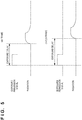
- extension mode 1 (comparative example) will be described with reference to Fig. 5 .
- the time (to be referred to as "exposure delay") from the transmission of an exposure permission signal to the exposure control apparatus 300 by the control apparatus 350 to the start of radiation irradiation (exposure) by the radiation source 400 can be different for each frame.
- the exposure delay in the (n+1)th frame is larger than the exposure delay in the nth frame.
- the fact that the exposure delay is different for each frame means that the periods T1 and T2 from the start of irradiation of the radiation 800 to the completion of the sampling and holding of the sample and hold circuits 270 and 280, respectively, vary. Therefore, the energy and irradiation amount (dose) of the radiation detected as each of the first signal 805, the second signal 806, and the third signal 807 can change between the frames.
- the energy and irradiation amount (dose) of the radiation detected as each of the irradiation amount e1, the irradiation amount e2, and the irradiation amount e3 change between the frames, so that the accuracy of energy subtraction based on the irradiation amount e1, the irradiation amount e2, and the irradiation amount e3 can be decreased. This can cause an artifact and/or blinking in the moving image.
- Fig. 6 shows the operation of the radiation imaging apparatus 1 in extension mode 2. Matters not mentioned as extension mode 2 can follow extension mode 1. In order to solve the problem in extension mode 1 (comparative example), it is required to cause the sample and hold circuits 270 and 280 of the pixel 112 to perform sampling and holding in synchronization with the radiation actually emitted from the radiation source 400 instead of the exposure permission signal.
- the control unit 130 determines the timing of each of a plurality of sample and hold operations SH1, SH2, and SH3 in each of the plurality of pixels 112 of the pixel array 110.
- the control unit 130 determines the timing of each of the plurality of sample and hold operations SH1, SH2, and SH3 in each of the plurality of pixels 112 of the pixel array 110. During the period between the first sample and hold operation SH1 of the plurality of sample and hold operations SH1, SH2, and SH3 and the last sample and hold operation of the plurality of sample and hold operations SH1, SH2, and SH3, the reset switch 220 does not reset the conversion element 210.
- the timing of at least one sample and hold operation of the plurality of sample and hold timings SH1, SH2, and SH3 is a timing in the radiation irradiation period TT.
- the timings of the two sample and hold timings SH1 and SH2 of the three sample and hold timings SH1, SH2, and SH3 are timings in the radiation irradiation period TT.
- the timings of the plurality of sample and hold operations SH1, SH2, and SH3 can be determined in accordance with elapsed times t1, t2, and t3 from the synchronization signal, respectively. Therefore, the period from the start of radiation irradiation to the end of the sample and hold operation SH1 is made constant between frames.
- the period from the start of radiation irradiation to the end of the sample and hold operation SH2 is made constant between frames. Furthermore, the period from the start of radiation irradiation to the end of the sample and hold operation SH3 is made constant between frames. This can suppress a decrease in accuracy of the energy subtraction, and reduce an artifact and/or blinking in a moving image.
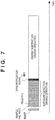
- Fig. 7 exemplarily shows a method of detecting, by the detection unit 190, the start of irradiation of radiation from the radiation source 400.
- the reset switch 220 is turned on by activating the reset signal PRES.
- an exposure detection driving operation is performed. If the start of radiation irradiation is detected in the exposure detection driving operation, the process transitions to an energy subtraction driving operation.
- the exposure detection driving operation includes repetition of "sampling and holding" by the sample and hold circuits 270 and 280 of the pixel 112 and “reading out” of the signal from the pixel 112 by the readout circuit RC.
- the exposure detection driving operation and the energy subtraction driving operation are controlled by the control unit 130.
- the detection unit 190 determines that radiation irradiation by the radiation source 400 has been started, and generates the synchronization signal 501.
- the control unit 130 starts the energy subtraction driving operation.
- the energy subtraction driving operation includes driving in response to the synchronization signal 501 shown in Fig. 5 , that is, the plurality of sample and hold operations SH1, SH2, and SH3 by the sample and hold circuits 270 and 280 of each of the plurality of pixels 112 and a readout operation by the readout circuit RC.
- the readout operation by the readout circuit RC includes an operation of outputting the first signal 805, the second signal 806, and the third signal 807.
- the repetition of "sampling and holding” and “reading out” in the exposure detection driving operation is preferably performed at a high speed (for example, ⁇ s order). This is because the timing at which the start of radiation irradiation is detected is delayed by the time required for "sampling and holding" and "reading out”.
- binning the number of pixels added during the reading out may be changed during the period of the exposure detection driving operation. As the number of pixels added increases as binning of 2 ⁇ 2, 4 ⁇ 4, 8 ⁇ 8,..., the readout time can be shortened.
- the resolution may be greatly reduced such as 32 ⁇ 32 binning to shorten the time required for reading out.
- the number of pixels 112 to be read out may be limited. For example, in order to read out the signals from the pixels in some rows, the other rows may be skipped.
- the process transitions from the exposure detection operation to the energy subtraction driving operation, so that settings for binning and the like are changed to those for the energy subtraction driving operation.
- the sample and hold circuit 270 may be or may not be reset.
- the synchronization signal 501 is generated in response to the signal read out from the pixel array 110 by the readout circuit RC exceeding a first threshold value, and the timing of the sample and hold operation SH1 can be determined accordingly. Thereafter, the timing of the sample and hold operation SH2 can be determined in response to the signal read out from the pixel array 110 by the readout circuit RC exceeding a second threshold value. Further, the timing of the sample and hold operation SH3 can be determined in response to the signal read out from the pixel array 110 by the readout circuit RC exceeding a third threshold value.
- extension mode 2 since the frame period is determined in accordance with the exposure delay, the frame period can be different between frames.
- the period from the activation of the reset signal PRES to the start of radiation irradiation depends on the exposure delay. This means that the noise level accumulated in the conversion element 210 from the activation of the reset signal PRES to the start of radiation irradiation depends on the exposure delay. Therefore, in extension mode 2, the noise level can be different between frames.
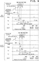
- Extension mode 3 is a mode in which the problem in extension mode 2, that is, the problem that the frame period can be different between frames has been solved.
- the frame rate is constant without depending on the exposure delay.
- the control unit 130 controls the readout circuit RC such that the timing at which the output of the third signal 807 is completed is common between frames.
- the control unit 130 controls the timing at which the readout circuit RC starts reading out the second signal 806, or controls the drive timing of the readout circuit RC so as to make the timing at which the readout circuit RC starts reading out the second signal 806 constant between frames. Accordingly, the timing at which the output of the third signal 807 is completed can be made constant between frames.
- control unit 130 may make the frame rate constant by adjusting the time from the completion of reading out of the third signal 807 to the timing at which the next frame starts (for example, the timing at which the reset signal PES is activated).
- the reset switch 220 does not reset the conversion element 210 during the period between the first sample and hold operation SH1 and the last sample and hold operation SH3 of the plurality of sample and hold operations SH1, SH2, and SH3.
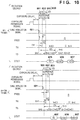
- Fig. 10 shows the operation of the radiation imaging apparatus 1 in extension mode 4. Matters not mentioned as extension mode 4 can follow extension mode 1.
- extension mode 4 the accumulation time from the activation of the reset signal PRES to the end of the sample and hold operation SH1 is constant between frames.
- extension mode 4 the accumulation time from the activation of the reset signal PRES to the end of the sample and hold operation SH2 is constant between frames.
- extension mode 4 the accumulation time from the activation of the reset signal PRES to the end of the sample and hold operation SH3 is constant between frames. Therefore, the noise level accumulated in the conversion element 210 is constant between frames without depending on the exposure delay.
- the frame rate is not constant in extension mode 4 described above, but the frame rate may be made constant in extension mode 4 as in extension mode 3.
- the reset switch 220 does not reset the conversion element 210 during the period between the first sample and hold operation SH1 and the last sample and hold operation SH3 of the plurality of sample and hold operations SH1, SH2, and SH3.
- the present invention is not limited to such an embodiment.
- four types of images having different energies may be obtained by increasing the number of sample and hold operations.
- two types of images having different energies may be obtained by decreasing the number of sample and hold operations.
- two types of images having different energies may be obtained from three types of images having different energies.
- a plurality of images having different energies are obtained by using the blunt leading and trailing edges of the tube voltage of the radiation source 400, and a new radiation image is formed based on the plurality of images.
- the plurality of images having different energies can be obtained by intentionally adjusting the waveform of the tube voltage of the radiation source 400.
- the plurality of images may be obtained by emitting radiation having a wide energy band (wavelength band) from the radiation source 400 and changing the energy of the radiation by changing a plurality of filters.
- the detection unit 190 detects the start of radiation irradiation by the radiation source 400 based on the radiation emitted from the radiation source 400.
- a detection unit 190 detects the start of radiation irradiation by a radiation source 400 based on information provided from the radiation source 400. That is, the detection unit 190 can be configured to detect the start of radiation irradiation by the radiation source 400 based on the radiation emitted from the radiation source 400 or information provided from the radiation source 400.
- Fig. 11 shows the arrangement of a radiation imaging apparatus 1 according to the second embodiment of the present invention. Matters not mentioned as the second embodiment can follow the first embodiment.
- the radiation source 400 provides driving current information indicating a driving current for generating radiation to a control apparatus 350 via a monitor line 410, for example.
- the radiation source 400 may be configured to provide the driving current information to the control apparatus 350 via an exposure control apparatus 300.
- the driving current is a current that flows between the cathode and the anode of the radiation source 400, and can be detected by an ammeter incorporated in the radiation source 400.
- the detection unit 190 may be provided in the control apparatus 350, provided in an imaging unit 100, or provided separately from the control apparatus 350 and the imaging unit 100.
- the driving current information can be provided from the radiation source 400 to the detection unit 190 via the control apparatus 350 or directly.
- the detection unit 190 can detect the start of radiation irradiation by the radiation source 400 and generate a synchronization signal 501 when a value indicated by information such as the driving current information provided from the radiation source 400 exceeds a threshold value.
- Fig. 12 shows the arrangement of a radiation imaging apparatus 1 according to the third embodiment of the present invention. Matters not mentioned as the third embodiment can follow the first embodiment.
- the radiation imaging apparatus 1 according to the third embodiment includes a radiation detection sensor 500 provided separately from a pixel array 110.
- the radiation detection sensor 500 may be arranged in an imaging unit 100 or may be arranged in a path between a radiation source 400 and the imaging unit 100.
- a detection unit 190 detects the start of radiation irradiation by the radiation source 400 based on the output from the radiation detection sensor 500, and generates a synchronization signal 501.
- the radiation detection sensor 500 may have energy resolution.
- the detection unit 190 can be configured to detect the start of radiation irradiation by the radiation source 400 based on the energy of the radiation detected by the radiation detection sensor 500. According to such an arrangement, a radiation image can be stably obtained even when the leading edge of the energy of the radiation emitted by the radiation source 400 varies or when the pulse width of the energy varies.
Landscapes
- Engineering & Computer Science (AREA)
- Health & Medical Sciences (AREA)
- Life Sciences & Earth Sciences (AREA)
- Multimedia (AREA)
- Signal Processing (AREA)
- Physics & Mathematics (AREA)
- High Energy & Nuclear Physics (AREA)
- Molecular Biology (AREA)
- Medical Informatics (AREA)
- General Physics & Mathematics (AREA)
- Spectroscopy & Molecular Physics (AREA)
- Nuclear Medicine, Radiotherapy & Molecular Imaging (AREA)
- Surgery (AREA)
- Optics & Photonics (AREA)
- Pathology (AREA)
- Radiology & Medical Imaging (AREA)
- Biomedical Technology (AREA)
- Heart & Thoracic Surgery (AREA)
- Biophysics (AREA)
- Animal Behavior & Ethology (AREA)
- General Health & Medical Sciences (AREA)
- Public Health (AREA)
- Veterinary Medicine (AREA)
- Mathematical Physics (AREA)
- Apparatus For Radiation Diagnosis (AREA)
- Transforming Light Signals Into Electric Signals (AREA)
- Measurement Of Radiation (AREA)
Abstract
Description
- The present invention relates to a radiation imaging apparatus.
- There is an energy subtraction method as an imaging method that applies a radiation imaging apparatus. The energy subtraction method is a method of obtaining new images (for example, a bone image and a soft tissue image) by processing a plurality of images obtained by capturing an object a plurality of times while changing energy of radiation to irradiate the object. A time interval during which a plurality of radiation images are captured is, for example, several seconds or more in a radiation imaging apparatus to capture a still image, about 100 msec in a general radiation imaging apparatus for a moving image, and about 10 msec even in a radiation imaging apparatus for a high-speed moving image. If the object moves in this time interval, an artifact is caused by that movement. It is therefore difficult to obtain, by the energy subtraction method, a radiation image of an object such as a heart that moves fast.
-
PTL 1 describes a system that performs dual energy imaging. In this system, the tube voltage of an X-ray source is set to the first kV value, and then changed to the second kV value in imaging. Then, the first signal corresponding to the first sub-image is integrated when the tube voltage is the first kV value, and integration is reset after the integrated signal is transferred to a sample and hold node. Subsequently, the second signal corresponding to the second sub-image is integrated when the tube voltage is the second kV value. Consequently, readout of the integrated first signal and integration of the second signal are performed parallelly. - When a plurality of frames of a moving image are captured by performing X-ray exposure a plurality of times using the method described in
PTL 1, the time from the X-ray exposure to the transfer of the signal to the sample and hold node can be different for each frame. Consequently, the energy and dose of the first sub-image differ between the frames, and the energy and dose of the second sub-image also differ between the frames. This can cause a decrease in accuracy of energy subtraction. - PTL 1: Japanese
PCT National Publication No. 2009-504221 - The present invention provides a technique advantageous in reducing variation in time from the start of radiation irradiation to sampling and holding of a signal.
- An aspect of the present invention relates to a radiation imaging apparatus comprising a pixel array including a plurality of pixels, and a readout circuit configured to read out signals from the pixel array. The radiation imaging apparatus comprises a detection unit configured to detect, based on radiation emitted from a radiation source or information provided from the radiation source, a start of irradiation of radiation by the radiation source, and a control unit configured to determine a timing of each of a plurality of sample and hold operations in each of the plurality of pixels each time the start of irradiation of radiation is detected by the detection unit, wherein the timing of at least one sample and hold operation of the plurality of sample and hold operations is a timing in a radiation irradiation period, and each of the plurality of pixels includes a conversion element configured to convert radiation into an electrical signal, and a sample and hold circuit configured to sample and hold the signal from the conversion element over a plurality of times in accordance with the timing of each of the plurality of sample and hold operations determined by the control unit.
-
-
Fig. 1 is a diagram showing the arrangement of a radiation imaging apparatus according to the first embodiment of the present invention; -
Fig. 2 is a view showing an example of the arrangement of an imaging unit; -
Fig. 3 is a circuit diagram showing an example of the arrangement of one pixel; -
Fig. 4 is a timing chart showing the operation of the radiation imaging apparatus in extension mode 1 (comparative example); -
Fig. 5 is a view for explaining a problem in extension mode 1 (comparative example); -
Fig. 6 is a timing chart showing the operation of the radiation imaging apparatus in extension mode 2; -
Fig. 7 is a view showing a method of detecting, by a detection unit, the start of irradiation of radiation from a radiation source; -
Fig. 8 is a timing chart for explaining a frame rate in extension mode 2; -
Fig. 9 is a timing chart showing the operation of the radiation imaging apparatus in extension mode 3; -
Fig. 10 is a timing chart showing the operation of the radiation imaging apparatus in extension mode 4; -
Fig. 11 is a diagram showing the arrangement of a radiation imaging apparatus according to the second embodiment of the present invention; and -
Fig. 12 is a diagram showing the arrangement of a radiation imaging apparatus according to the third embodiment of the present invention. - Exemplary embodiments of the present invention will be explained below with reference to the accompanying drawings.
-
Fig. 1 shows the arrangement of aradiation imaging apparatus 1 according to the first embodiment of the present invention. Theradiation imaging apparatus 1 can include animaging unit 100 including apixel array 110 including a plurality of pixels and asignal processing unit 352 that processes a signal from theimaging unit 100. Theimaging unit 100 can have, for example, a panel shape. As exemplified inFig. 1 , thesignal processing unit 352 may be arranged as part of acontrol apparatus 350, incorporated in the same housing as theimaging unit 100, or incorporated in a housing different from that of theimaging unit 100 and thecontrol apparatus 350. Theradiation imaging apparatus 1 is an apparatus for obtaining a radiation image by an energy subtraction method. The energy subtraction method is a method of obtaining new radiation images (for example, a bone image and a soft tissue image) by processing a plurality of images obtained by capturing an object a plurality of times while changing energy of radiation to irradiate the object. The term "radiation" can include, for example, α-rays, β-rays, γ-rays, particle rays, and cosmic rays in addition to X-rays. - The
radiation imaging apparatus 1 can include aradiation source 400 that generates radiation, anexposure control apparatus 300 that controls theradiation source 400, and thecontrol apparatus 350 that controls the exposure control apparatus 300 (the radiation source 400) and theimaging unit 100. As described above, thecontrol apparatus 350 can include thesignal processing unit 352 that processes a signal supplied from theimaging unit 100. All or some functions of thecontrol apparatus 350 can be incorporated in theimaging unit 100. Alternatively, some functions of theimaging unit 100 can be incorporated in thecontrol apparatus 350. Thecontrol apparatus 350 can be formed by a computer (processor) and a memory that stores programs provided for the computer. Thesignal processing unit 352 can be made of some of the programs. Alternatively, thesignal processing unit 352 can be made of a computer (processor) and a memory that stores programs provided for the computer. Thecontrol apparatus 350 may be formed by a DSP (digital signal processor) or a PLA (programmable logic array) entirely or partially. Thecontrol apparatus 350 and thesignal processing unit 352 may be designed and manufactured by a logic synthesis tool based on a file that describes their operations. - When permitting radiation irradiation (exposure) by the
radiation source 400, thecontrol apparatus 350 transmits an exposure permission signal to theexposure control apparatus 300. When the exposure permission signal is received from thecontrol apparatus 350, theexposure control apparatus 300 causes theradiation source 400 to perform radiation irradiation (exposure) in response to the reception of the exposure permission signal. When capturing a moving image, thecontrol apparatus 350 transmits an exposure permission signal to the exposure control apparatus 300 a plurality of times. In this case, thecontrol apparatus 350 may transmit an exposure permission signal to the exposure control apparatus 300 a plurality of times at a predetermined cycle, or may transmit an exposure permission signal to theexposure control apparatus 300 each time theimaging unit 100 can capture the next frame. - The
radiation source 400 can emit radiation whose energy (wavelength) changes in a continuous radiation period (irradiation period) of the radiation. By using such radiation, radiation images are obtained at a plurality of energies different from each other, and these radiation images are processed by the energy subtraction method, thereby obtaining a new radiation image. - Alternatively, the
radiation source 400 may have a function of changing radiation energy (wavelength). Theradiation source 400 can have a function of changing the radiation energy by changing, for example, a tube voltage (a voltage applied between the cathode and anode of the radiation source 400). - Each of the plurality of pixels forming the
pixel array 110 of theimaging unit 100 includes a conversion element that converts radiation into an electrical signal (for example, charges) and a reset unit that resets the conversion element. Each pixel may be configured to convert the radiation into the electrical signal directly or may be configured to convert the radiation into light such as visible light, and then convert the light into the electrical signal. In the latter case, a scintillator for converting radiation into light can be used. The plurality of pixels that form thepixel array 110 can share the scintillator. -
Fig. 2 shows an example of the arrangement of theimaging unit 100. Theimaging unit 100 includes thepixel array 110 including a plurality ofpixels 112 and a readout circuit RC that reads out signals from the plurality ofpixels 112 of thepixel array 110. The plurality ofpixels 112 can be arrayed to form a plurality of rows and a plurality of columns. The readout circuit RC can include arow selection circuit 120, acontrol unit 130, abuffer circuit 140, acolumn selection circuit 150, anamplification unit 160, anAD converter 170, and adetection unit 190. - The
row selection circuit 120 selects a row of thepixel array 110. Therow selection circuit 120 can be arranged to select a row by driving arow control signal 122. Thebuffer circuit 140 buffers signals from thepixels 112 of one of the plurality of rows of thepixel array 110, which is selected by therow selection circuit 120. Thebuffer circuit 140 buffers the signals of a plurality of columns output to a plurality of columnsignal transmission paths 114 of thepixel array 110. The columnsignal transmission path 114 in each column includes a first signal line and a second column signal line which form a column signal line pair. A noise level (at the time of a normal mode to be described later) of thepixel 112 or a radiation signal (at the time of an extension mode to be described later) corresponding to the radiation detected in thepixel 112 can be output to the first column signal line. A radiation signal corresponding to the radiation detected in thepixel 112 can be output to a secondcolumn signal line 322. Thebuffer circuit 140 can include an amplifier circuit. - The
column selection circuit 150 selects, in a predetermined order, signal pairs of one row buffered by thebuffer circuit 140. Theamplification unit 160 amplifies the signal pairs selected by thecolumn selection circuit 150. In this case, theamplification unit 160 can be arranged as a differential amplifier that amplifies the difference of a signal pair (two signals). TheAD converter 170 can include theAD converter 170 that A/D-converts a signal OUT output from theamplification unit 160 and outputs a digital signal DOUT (a radiation image signal). - The
detection unit 190 detects the start of radiation irradiation by theradiation source 400 based on the radiation emitted from theradiation source 400. Thedetection unit 190 can detect the start of radiation irradiation by theradiation source 400 by detecting, for example, the radiation emitted from theradiation source 400 toward thepixel array 110 based on a signal read out from thepixel array 110 by the readout circuit RC. Alternatively, thedetection unit 190 can detect the start of radiation irradiation by theradiation source 400 based on a current flowing through a bias line that supplies a bias voltage to each pixel. When the start of radiation irradiation by theradiation source 400 is detected, thedetection unit 190 generates a synchronization signal indicating the start and supplies it to thecontrol unit 130. -
Fig. 3 shows an example of the arrangement of onepixel 112. Thepixel 112 includes, for example, aconversion element 210, a reset switch 220 (reset unit), anamplifier circuit 230, asensitivity changing unit 240, aclamp circuit 260, sample and hold circuits (holding portions) 270 and 280, and anoutput circuit 310. Eachpixel 112 can have the normal mode and the extension mode as the modes concerning the imaging method. The extension mode is a mode for obtaining a radiation image in accordance with the energy subtraction method. - The
conversion element 210 converts radiation into an electrical signal. Theconversion element 210 can be formed by, for example, a scintillator that can be shared by the plurality of pixels and a photoelectric conversion element. Theconversion element 210 includes a charge accumulation portion that accumulates a converted electrical signal (charges), that is, an electrical signal corresponding to radiation. The charge accumulation portion is connected to the input terminal of theamplifier circuit 230. - The
amplifier circuit 230 can includeMOS transistors 235 and 236, and acurrent source 237. The MOS transistor 235 is connected to thecurrent source 237 via theMOS transistor 236. The MOS transistor 235 and thecurrent source 237 form a source follower circuit. TheMOS transistor 236 is an enable switch which is turned on by activating an enable signal EN, and sets the source follower circuit formed by the MOS transistor 235 and thecurrent source 237 in an operation state. - The charge accumulation portion of the
conversion element 210 and the gate of the MOS transistor 235 function as a charge/voltage conversion unit CVC that converts charges accumulated in the charge accumulation portion into a voltage. That is, a voltage V (= Q/C) determined by charges Q accumulated in the charge accumulation portion and a capacitance value C of the charge/voltage conversion unit appears in the charge/voltage conversion unit CVC. The charge/voltage conversion unit CVC is connected to a reset potential Vres via thereset switch 220. When a reset signal PRES is activated, thereset switch 220 is turned on, and the potential of the charge/voltage conversion unit is reset to the reset potential Vres. Thereset switch 220 can include a transistor that has the first main electrode (drain) connected to the charge accumulation portion of theconversion element 210, the second main electrode (source) to which the reset potential Vres is applied, and a control electrode (gate). The transistor electrically connects the first main electrode and the second main electrode by receiving an ON voltage at the control electrode, and resets the charge accumulation portion of theconversion element 210. - The
clamp circuit 260 clamps, by aclamp capacitor 261, a reset noise level output from theamplifier circuit 230 in accordance with the potential of the reset charge/voltage conversion unit CVC. Theclamp circuit 260 is a circuit configured to cancel the reset noise level from a signal (radiation signal) output from theamplifier circuit 230 in accordance with charges (electrical signal) converted by theconversion element 210. The reset noise level includes kTC noise at the time of reset of the charge/voltage conversion unit CVC. A clamp operation is performed by turning on aMOS transistor 262 by activating a clamp signal PCL, and then turning off theMOS transistor 262 by deactivating the clamp signal PCL. - The output side of the
clamp capacitor 261 is connected to the gate of aMOS transistor 263. The source of theMOS transistor 263 is connected to acurrent source 265 via aMOS transistor 264. TheMOS transistor 263 and thecurrent source 265 form a source follower circuit. TheMOS transistor 264 is an enable switch which is turned on by activating an enable signal EN0 supplied to its gate, and sets the source follower circuit formed by theMOS transistor 263 and thecurrent source 265 in an operation state. - The
output circuit 310 includesMOS transistors 311, 313, and 315 and row selection switches 312 and 314. TheMOS transistors 311, 313, and 315, respectively, form source follower circuits with current sources (not shown) connected tocolumn signal lines - The sample and hold
circuit 280 can sample and hold (hold) a radiation signal as a signal output from theclamp circuit 260 in accordance with charges generated in theconversion element 210. The sample and holdcircuit 280 can include aswitch 281 and acapacitor 282. Theswitch 281 is turned on when a sample and hold signal TS is activated by therow selection circuit 120. The radiation signal output from theclamp circuit 260 is written in thecapacitor 282 via theswitch 281 by activating the sample and hold signal TS. - In the normal mode, in the state in which the
reset switch 220 resets the potential of the charge/voltage conversion unit CVC and theMOS transistor 262 is ON, theclamp circuit 260 outputs the noise level (offset component) of theclamp circuit 260. The sample and holdcircuit 270 can sample and hold (hold) the noise level of theclamp circuit 260. The sample and holdcircuit 270 can include aswitch 271 and acapacitor 272. Theswitch 271 is turned on when a sample and hold signal TN is activated by therow selection circuit 120. A noise level output from theclamp circuit 260 is written in thecapacitor 272 via theswitch 271 by activating the sample and hold signal TN. In the extension mode, the sample and holdcircuit 270 can also be used to hold a radiation signal as a signal output from theclamp circuit 260 in accordance with charges generated in theconversion element 210. - When row selection signals VST are activated, signals corresponding to signals held by the sample and hold
circuits column signal line 321 and the secondcolumn signal line 322 that form the columnsignal transmission paths 114. More specifically, a signal N corresponding to a signal (a noise level or a radiation signal) held by the sample and holdcircuit 270 is output to thecolumn signal line 321 via theMOS transistor 311 and therow selection switch 312. A signal S corresponding to a signal held by the sample and holdcircuit 280 is output to thecolumn signal line 322 via the MOS transistor 313 and therow selection switch 314. - The
pixel 112 may include addition switches 301 and 302 configured to add signals of the plurality ofpixels 112. In an addition mode, addition mode signals ADDN and ADDS are activated. Thecapacitors 272 of the plurality ofpixels 112 are connected to each other by activating the addition mode signal ADDN, averaging the signals (noise level or radiation signal). Thecapacitors 282 of the plurality ofpixels 112 are connected to each other by activating the addition mode signal ADDS, averaging the radiation signals. - The
pixel 112 can include thesensitivity changing unit 240. Thesensitivity changing unit 240 can includeswitches capacitors MOS transistors switch 241 is turned on, and the capacitance value of the firstadditional capacitor 243 is added to the capacitance value of the charge/voltage conversion unit CVC. Consequently, the sensitivity of thepixel 112 is decreased. Further, when a second change signal WIDE2 is also activated, theswitch 242 is also turned on, and the capacitance value of the secondadditional capacitor 244 is added to the capacitance value of the charge/voltage conversion unit CVC. Consequently, the sensitivity of thepixel 112 is further decreased. A dynamic range can be widened by adding a function of decreasing the sensitivity of thepixel 112. An enable signal ENW may be activated when the first change signal WIDE is activated. In this case, theMOS transistor 246 performs a source follower operation. Note that when theswitch 241 of thesensitivity changing unit 240 is turned on, the potential of the charge accumulation portion of theconversion element 210 may be changed by charge redistribution. Consequently, some signals may be destructed. - The above-described reset signal Pres, enable signal EN, clamp signal PCL, enable signal EN0, sample and hold signals TN and TS, and row selection signals VST are control signals controlled (driven) by the
row selection circuit 120 and correspond to the row control signals 122 ofFig. 2 . Therow selection circuit 120 generates the reset signal Pres, enable signal EN, clamp signal PCL, enable signal EN0, sample and hold signals TN and TS, and row selection signals VST in accordance with the timing signal supplied from thecontrol unit 130. - In the
pixel 112 having the arrangement as shown inFig. 3 , signals are not destructed in, for example, the charge accumulation portion of theconversion element 210 in a sample and hold operation. That is, in thepixel 112 having the arrangement as shown inFig. 3 , the radiation signals can be nondestructively read out. Such an arrangement is advantageous to radiation imaging to which the energy subtraction method is applied to be described below. - The extension mode for obtaining a radiation image in accordance with the energy subtraction method will be described below. The extension mode can include the following four sub-modes (
extension modes 1, 2, 3, and 4). Here,extension mode 1 is a comparative example, and extension modes 2, 3, and 4 are improved examples of comparative example 1. -
Fig. 4 shows the operation of theradiation imaging apparatus 1 in extension mode 1 (comparative example). InFig. 4 , the abscissa indicates a time. "Radiation energy" is energy of radiation which is emitted from theradiation source 400 and irradiates theimaging unit 100. "PRES" is the reset signal RPES. "TS" is the sample and hold signal TS. "DOUT" is an output of theAD converter 170. Thecontrol apparatus 350 that generates an exposure permission signal can control synchronization of radiation emission from theradiation source 400 and the operation of theimaging unit 100. Thecontrol unit 130 controls an operation in theimaging unit 100. The clamp signal PCL is also activated over a predetermined period in a period during which the reset signal PRES is activated, and theclamp circuit 260 clamps a noise level. - As shown in the example of
Fig. 4 , the energy (wavelength) ofradiation 800 emitted from theradiation source 400 changes in the radiation period of the radiation. This is caused by the blunt leading and trailing edges of the tube voltage of theradiation source 400. For this reason, assume that theradiation 800 is made fromradiation 801 in a leading period,radiation 802 in a stable period, andradiation 803 in a trailing period. Energy E1 of theradiation 801, energy E2 of theradiation 802, and energy E3 of theradiation 803 can be different from each other. By using this, a radiation image according to the energy subtraction method can be obtained. - The
control unit 130 defines a first period T1, a second period T2, and a third period T3 such that the first period T1, second period T2, and third period T3 correspond to the leading period, stable period, and trailing period, respectively. Eachpixel 112 executes an operation of outputting a first signal corresponding to an electrical signal generated by theconversion element 210 in the first period T1. Further, eachpixel 112 executes an operation of outputting a second signal corresponding to an electrical signal generated by theconversion element 210 in the first period T1 and second period T2. Furthermore, eachpixel 112 executes an operation of outputting a third signal corresponding to an electrical signal generated by theconversion element 210 in the first period T1, second period T2, and third period T3. The first period T1, second period T2, and third period T3 are periods different from each other. It is planned that radiation having the first energy E1 is emitted in the first period T1, radiation having the second energy E2 is emitted in the second period T2, and radiation having the second energy E3 is emitted in the third period T3. - In
extension mode 1, theconversion element 210 of eachpixel 112 is not reset (the reset signal Pres is not activated) in an irradiation period TT of theradiation 800. Accordingly, in the irradiation period TT of theradiation 800, an electrical signal (charges) corresponding to the incident radiation is kept accumulated in theconversion element 210. In the irradiation period TT of theradiation 800, since theconversion element 210 of eachpixel 112 is not reset, it is advantageous in reducing the irradiation of the radiation which does not contribute to the imaging and obtaining a radiation image for the energy subtraction method within a shorter time. - Before emission (irradiation for the imaging unit 100) of the
radiation 800, the reset signal PRES is activated for a predetermined period and accordingly theconversion element 210 is reset. At this time, the clamp signal PCL is also activated for the predetermined period, and theclamp circuit 260 is clamped to the reset level (the noise level). - After the reset signal PRES is activated for the predetermined period, an exposure permission signal is transmitted from the
exposure control apparatus 300 to theradiation source 400, and the radiation is emitted from theradiation source 400 in response to the exposure permission signal. When the predetermined period has elapsed upon activation of the reset signal PRES for the predetermined period, the sample and hold signal TN is activated for the predetermined period. Accordingly, upon reception of irradiation of theradiation 801 having the energy E1, a signal (E1) corresponding to an electrical signal generated by theconversion element 210 of thepixel 112 of thepixel array 110 is sampled and held by the sample and holdcircuit 270. - When the predetermined period has elapsed upon activation of the sample and hold signal TN for the predetermined period, the sample and hold signal TS is activated for the predetermined period. Accordingly, upon reception of irradiation of the
radiation 801 having the energy E1 and theradiation 802 having the energy E2, a signal (E1 + E2) corresponding to an electrical signal generated by theconversion element 210 of thepixel 112 of thepixel array 110 is sampled and held by the sample and holdcircuit 280. - Next, a signal corresponding to the difference between the signal (E1) sampled and held by the sample and hold
circuit 270 and the signal (E1 + E2) sampled and held by the sample and holdcircuit 280 is output from the readout circuit RC as afirst signal 805. Referring toFig. 4 , "N" indicates a signal sampled and held by the sample and holdcircuit 270 and output to the firstcolumn signal line 321, and "S" indicates a signal sampled and held by the sample and holdcircuit 280 and output to the secondcolumn signal line 322. - When the predetermined period has elapsed upon activation of the sample and hold signal TS for the predetermined period (upon completion of irradiation (irradiation of the radiation 800) of the
radiation 803 having the energy E3), the sample and hold signal TS is activated for the predetermined period again. Accordingly, upon reception of irradiation of theradiation 801 having the energy E1, theradiation 802 having the energy E2, and theradiation 803 having the energy E3, a signal (E1 + E2 + E3) corresponding to an electrical signal generated by theconversion element 210 of thepixel 112 of thepixel array 110 is sampled and held by the sample and holdcircuit 280. - Next, a signal corresponding to the difference between the signal (E1) sampled and held by the sample and hold
circuit 270 and the signal (E1 + E2 + E3) sampled and held by the sample and holdcircuit 280 is output from the readout circuit RC as asecond signal 806. - Next, the reset signal PRES is activated for the predetermined period, and then the sample and hold signal TN is activated for the predetermined period. Accordingly, the reset level (0) is sampled and held by the sample and hold
circuit 270. Next, a signal corresponding to the difference between the signal (0) sampled and held by the sample and holdcircuit 270 and the signal (E1 + E2 + E3) sampled and held by the sample and holdcircuit 280 is output from the readout circuit RC as athird signal 807. - By repeating the above operation a plurality of times, radiation images of a plurality of frames (that is, a moving image) can be obtained.
- The
signal processing unit 352 can obtain the first signal 805 (E2), the second signal 806 (E2 + E3), and the third signal 807 (E1 + E2 + E3) as described above. Thesignal processing unit 352 can obtain an irradiation amount e1 of theradiation 801 having the energy E1, an irradiation amount e2 of theradiation 802 having the energy E2, and an irradiation amount e3 of theradiation 803 having the energy E3 based on thefirst signal 805, thesecond signal 806, and thethird signal 807. More specifically, thesignal processing unit 352 calculates a difference ((E2 + E3) - E2) between the first signal 805 (E2) and the second signal (E2 + E3) to obtain the irradiation amount e3 of theradiation 803 having the energy E3. Thesignal processing unit 352 calculates a difference ((E1 + E2 + E3) - (E2 + E3)) between the second signal 806 (E2 + E3) and the third signal (E1 + E2 + E3) to obtain the irradiation amount e1 of theradiation 801 having the energy E1. The first signal 805 (E2) indicates the irradiation amount e2 of theradiation 802 having the energy E2. - Therefore, the
signal processing unit 352 can obtain the radiation image by the energy subtraction method based on the irradiation amount e1 of theradiation 801 having the energy E1, the irradiation amount e2 of theradiation 802 having the energy E2, and the irradiation amount e3 of theradiation 803 having the energy E3. The energy subtraction method can be selected from various methods. For example, it is possible, by calculating a difference between the radiation image of the first energy and the radiation image of the second energy, to obtain a bone image and a soft tissue image. The bone image and the soft tissue image may be generated by solving nonlinear simultaneous equations based on the radiation image of the first energy and the radiation image of the second energy. It is also possible to obtain a contrast medium image and the soft tissue image based on the radiation image of the first energy and the radiation image of the second energy. It is also possible to obtain an electron density image and an effective atomic number image based on the radiation image of the first energy and the radiation image of the second energy. - The problem in extension mode 1 (comparative example) will be described with reference to
Fig. 5 . As shown in the example ofFig. 5 , the time (to be referred to as "exposure delay") from the transmission of an exposure permission signal to theexposure control apparatus 300 by thecontrol apparatus 350 to the start of radiation irradiation (exposure) by theradiation source 400 can be different for each frame. In the example shown inFig. 5 , the exposure delay in the (n+1)th frame is larger than the exposure delay in the nth frame. - When explained with reference to
Fig. 4 , the fact that the exposure delay is different for each frame means that the periods T1 and T2 from the start of irradiation of theradiation 800 to the completion of the sampling and holding of the sample and holdcircuits first signal 805, thesecond signal 806, and thethird signal 807 can change between the frames. This means that the energy and irradiation amount (dose) of the radiation detected as each of the irradiation amount e1, the irradiation amount e2, and the irradiation amount e3 change between the frames, so that the accuracy of energy subtraction based on the irradiation amount e1, the irradiation amount e2, and the irradiation amount e3 can be decreased. This can cause an artifact and/or blinking in the moving image. -
Fig. 6 shows the operation of theradiation imaging apparatus 1 in extension mode 2. Matters not mentioned as extension mode 2 can followextension mode 1. In order to solve the problem in extension mode 1 (comparative example), it is required to cause the sample and holdcircuits pixel 112 to perform sampling and holding in synchronization with the radiation actually emitted from theradiation source 400 instead of the exposure permission signal. Each time asynchronization signal 501 is supplied from thedetection unit 190, thecontrol unit 130 determines the timing of each of a plurality of sample and hold operations SH1, SH2, and SH3 in each of the plurality ofpixels 112 of thepixel array 110. In other words, each time the start of radiation irradiation is detected by thedetection unit 190, thecontrol unit 130 determines the timing of each of the plurality of sample and hold operations SH1, SH2, and SH3 in each of the plurality ofpixels 112 of thepixel array 110. During the period between the first sample and hold operation SH1 of the plurality of sample and hold operations SH1, SH2, and SH3 and the last sample and hold operation of the plurality of sample and hold operations SH1, SH2, and SH3, thereset switch 220 does not reset theconversion element 210. - Here, in order to obtain a radiation image by the energy subtraction method, the timing of at least one sample and hold operation of the plurality of sample and hold timings SH1, SH2, and SH3 is a timing in the radiation irradiation period TT. In the first embodiment, the timings of the two sample and hold timings SH1 and SH2 of the three sample and hold timings SH1, SH2, and SH3 are timings in the radiation irradiation period TT. The timings of the plurality of sample and hold operations SH1, SH2, and SH3 can be determined in accordance with elapsed times t1, t2, and t3 from the synchronization signal, respectively. Therefore, the period from the start of radiation irradiation to the end of the sample and hold operation SH1 is made constant between frames. Further, the period from the start of radiation irradiation to the end of the sample and hold operation SH2 is made constant between frames. Furthermore, the period from the start of radiation irradiation to the end of the sample and hold operation SH3 is made constant between frames. This can suppress a decrease in accuracy of the energy subtraction, and reduce an artifact and/or blinking in a moving image.
-
Fig. 7 exemplarily shows a method of detecting, by thedetection unit 190, the start of irradiation of radiation from theradiation source 400. Thereset switch 220 is turned on by activating the reset signal PRES. After the "reset" of the charge accumulation portion of theconversion element 210, an exposure detection driving operation is performed. If the start of radiation irradiation is detected in the exposure detection driving operation, the process transitions to an energy subtraction driving operation. The exposure detection driving operation includes repetition of "sampling and holding" by the sample and holdcircuits pixel 112 and "reading out" of the signal from thepixel 112 by the readout circuit RC. The exposure detection driving operation and the energy subtraction driving operation are controlled by thecontrol unit 130. When the signal read out from thepixel 112 by the readout circuit RC exceeds a threshold value, thedetection unit 190 determines that radiation irradiation by theradiation source 400 has been started, and generates thesynchronization signal 501. In response to this, thecontrol unit 130 starts the energy subtraction driving operation. The energy subtraction driving operation includes driving in response to thesynchronization signal 501 shown inFig. 5 , that is, the plurality of sample and hold operations SH1, SH2, and SH3 by the sample and holdcircuits pixels 112 and a readout operation by the readout circuit RC. Here, the readout operation by the readout circuit RC includes an operation of outputting thefirst signal 805, thesecond signal 806, and thethird signal 807. - The repetition of "sampling and holding" and "reading out" in the exposure detection driving operation is preferably performed at a high speed (for example, µs order). This is because the timing at which the start of radiation irradiation is detected is delayed by the time required for "sampling and holding" and "reading out". In order to increase the speed, binning (the number of pixels added) during the reading out may be changed during the period of the exposure detection driving operation. As the number of pixels added increases as binning of 2 × 2, 4 × 4, 8 × 8,..., the readout time can be shortened. Since the image obtained by reading out in the exposure detection driving operation is used to determine presence/absence of X-ray exposure for determining the start of radiation irradiation, it is not necessary to consider the resolution. Therefore, the resolution may be greatly reduced such as 32 × 32 binning to shorten the time required for reading out. Further, the number of
pixels 112 to be read out may be limited. For example, in order to read out the signals from the pixels in some rows, the other rows may be skipped. - When the
detection unit 190 outputs thesynchronization signal 501, the process transitions from the exposure detection operation to the energy subtraction driving operation, so that settings for binning and the like are changed to those for the energy subtraction driving operation. At this time, the sample and holdcircuit 270 may be or may not be reset. - In an example different from the above, the
synchronization signal 501 is generated in response to the signal read out from thepixel array 110 by the readout circuit RC exceeding a first threshold value, and the timing of the sample and hold operation SH1 can be determined accordingly. Thereafter, the timing of the sample and hold operation SH2 can be determined in response to the signal read out from thepixel array 110 by the readout circuit RC exceeding a second threshold value. Further, the timing of the sample and hold operation SH3 can be determined in response to the signal read out from thepixel array 110 by the readout circuit RC exceeding a third threshold value. - As shown in
Fig. 8 , in extension mode 2, since the frame period is determined in accordance with the exposure delay, the frame period can be different between frames. In addition, in extension mode 2, the period from the activation of the reset signal PRES to the start of radiation irradiation depends on the exposure delay. This means that the noise level accumulated in theconversion element 210 from the activation of the reset signal PRES to the start of radiation irradiation depends on the exposure delay. Therefore, in extension mode 2, the noise level can be different between frames. -
Fig. 9 shows the operation of theradiation imaging apparatus 1 in extension mode 3. Matters not mentioned as extension mode 3 can followextension mode 1. Extension mode 3 is a mode in which the problem in extension mode 2, that is, the problem that the frame period can be different between frames has been solved. In extension mode 3, the frame rate is constant without depending on the exposure delay. In extension mode 3, thecontrol unit 130 controls the readout circuit RC such that the timing at which the output of thethird signal 807 is completed is common between frames. For example, thecontrol unit 130 controls the timing at which the readout circuit RC starts reading out thesecond signal 806, or controls the drive timing of the readout circuit RC so as to make the timing at which the readout circuit RC starts reading out thesecond signal 806 constant between frames. Accordingly, the timing at which the output of thethird signal 807 is completed can be made constant between frames. - Instead of the above method, the
control unit 130 may make the frame rate constant by adjusting the time from the completion of reading out of thethird signal 807 to the timing at which the next frame starts (for example, the timing at which the reset signal PES is activated). - Also in extension mode 3, the
reset switch 220 does not reset theconversion element 210 during the period between the first sample and hold operation SH1 and the last sample and hold operation SH3 of the plurality of sample and hold operations SH1, SH2, and SH3. -
Fig. 10 shows the operation of theradiation imaging apparatus 1 in extension mode 4. Matters not mentioned as extension mode 4 can followextension mode 1. In extension mode 4, the accumulation time from the activation of the reset signal PRES to the end of the sample and hold operation SH1 is constant between frames. Further, in extension mode 4, the accumulation time from the activation of the reset signal PRES to the end of the sample and hold operation SH2 is constant between frames. Furthermore, in extension mode 4, the accumulation time from the activation of the reset signal PRES to the end of the sample and hold operation SH3 is constant between frames. Therefore, the noise level accumulated in theconversion element 210 is constant between frames without depending on the exposure delay. Note that the frame rate is not constant in extension mode 4 described above, but the frame rate may be made constant in extension mode 4 as in extension mode 3. - Also in extension mode 4, the
reset switch 220 does not reset theconversion element 210 during the period between the first sample and hold operation SH1 and the last sample and hold operation SH3 of the plurality of sample and hold operations SH1, SH2, and SH3. - In the above description, the embodiment in which three types of images having different energies are obtained has been described. However, the present invention is not limited to such an embodiment. For example, four types of images having different energies may be obtained by increasing the number of sample and hold operations. Alternatively, two types of images having different energies may be obtained by decreasing the number of sample and hold operations. Alternatively, two types of images having different energies may be obtained from three types of images having different energies.
- In the above example, a plurality of images having different energies are obtained by using the blunt leading and trailing edges of the tube voltage of the
radiation source 400, and a new radiation image is formed based on the plurality of images. The plurality of images having different energies can be obtained by intentionally adjusting the waveform of the tube voltage of theradiation source 400. Alternatively, the plurality of images may be obtained by emitting radiation having a wide energy band (wavelength band) from theradiation source 400 and changing the energy of the radiation by changing a plurality of filters. - In the first embodiment, the
detection unit 190 detects the start of radiation irradiation by theradiation source 400 based on the radiation emitted from theradiation source 400. In the second and third embodiments to be described below, adetection unit 190 detects the start of radiation irradiation by aradiation source 400 based on information provided from theradiation source 400. That is, thedetection unit 190 can be configured to detect the start of radiation irradiation by theradiation source 400 based on the radiation emitted from theradiation source 400 or information provided from theradiation source 400. -
Fig. 11 shows the arrangement of aradiation imaging apparatus 1 according to the second embodiment of the present invention. Matters not mentioned as the second embodiment can follow the first embodiment. In the second embodiment, theradiation source 400 provides driving current information indicating a driving current for generating radiation to acontrol apparatus 350 via amonitor line 410, for example. Theradiation source 400 may be configured to provide the driving current information to thecontrol apparatus 350 via anexposure control apparatus 300. The driving current is a current that flows between the cathode and the anode of theradiation source 400, and can be detected by an ammeter incorporated in theradiation source 400. For example, thedetection unit 190 may be provided in thecontrol apparatus 350, provided in animaging unit 100, or provided separately from thecontrol apparatus 350 and theimaging unit 100. When thedetection unit 190 is provided in theimaging unit 100, the driving current information can be provided from theradiation source 400 to thedetection unit 190 via thecontrol apparatus 350 or directly. Thedetection unit 190 can detect the start of radiation irradiation by theradiation source 400 and generate asynchronization signal 501 when a value indicated by information such as the driving current information provided from theradiation source 400 exceeds a threshold value. -
Fig. 12 shows the arrangement of aradiation imaging apparatus 1 according to the third embodiment of the present invention. Matters not mentioned as the third embodiment can follow the first embodiment. Theradiation imaging apparatus 1 according to the third embodiment includes aradiation detection sensor 500 provided separately from apixel array 110. Theradiation detection sensor 500 may be arranged in animaging unit 100 or may be arranged in a path between aradiation source 400 and theimaging unit 100. Adetection unit 190 detects the start of radiation irradiation by theradiation source 400 based on the output from theradiation detection sensor 500, and generates asynchronization signal 501. - The
radiation detection sensor 500 may have energy resolution. In this case, thedetection unit 190 can be configured to detect the start of radiation irradiation by theradiation source 400 based on the energy of the radiation detected by theradiation detection sensor 500. According to such an arrangement, a radiation image can be stably obtained even when the leading edge of the energy of the radiation emitted by theradiation source 400 varies or when the pulse width of the energy varies. - 1: radiation imaging apparatus, 110: pixel array, RC: readout circuit, 190: detection unit, 130: control unit, 210: conversion element, 270, 280: sample and hold circuit
Claims (10)
- A radiation imaging apparatus comprising a pixel array including a plurality of pixels, and a readout circuit configured to read out signals from the pixel array, characterized by comprising:a detection unit configured to detect, based on radiation emitted from a radiation source or information provided from the radiation source, a start of irradiation of radiation by the radiation source; anda control unit configured to determine a timing of each of a plurality of sample and hold operations in each of the plurality of pixels each time the start of irradiation of radiation is detected by the detection unit,wherein the timing of at least one sample and hold operation of the plurality of sample and hold operations is a timing in a radiation irradiation period, andeach of the plurality of pixels includes a conversion element configured to convert radiation into an electrical signal, and a sample and hold circuit configured to sample and hold the signal from the conversion element over a plurality of times in accordance with the timing of each of the plurality of sample and hold operations determined by the control unit.
- The radiation imaging apparatus according to claim 1, characterized in that
each of the plurality of pixels further includes a reset unit configured to reset the conversion element, and
in each of the plurality of pixels, the reset unit does not reset the conversion element in a period between the first sample and hold operation of the plurality of sample and hold operations and the last sample and hold operation of the plurality of sample and hold operations. - The radiation imaging apparatus according to claim 1 or 2, characterized in that the control unit determines the timing of each of the plurality of sample and hold operations such that radiation images having different energies can be obtained.
- The radiation imaging apparatus according to any one of claims 1 to 3, characterized in that the detection unit detects a start of irradiation of radiation by the radiation source based on an electrical signal obtained from the pixel array.
- The radiation imaging apparatus according to any one of claims 1 to 3, characterized in that the detection unit detects a start of irradiation of radiation by the radiation source based on a driving current for generating radiation in the radiation source.
- The radiation imaging apparatus according to any one of claims 1 to 3, characterized by further comprising a radiation detection sensor provided separately from the pixel array,
wherein the detection unit detects a start of irradiation of radiation by the radiation source based on an output from the radiation detection sensor. - The radiation imaging apparatus according to claim 6, characterized in that
the radiation detection sensor has energy resolution, and
the detection unit detects a start of irradiation of radiation by the radiation source based on an energy of radiation detected by the radiation detection sensor. - The radiation imaging apparatus according to any one of claims 1 to 7, characterized in that the control unit controls the plurality of pixels so as to make a frame rate constant.
- The radiation imaging apparatus according to claim 2, characterized in that the control unit controls the plurality of pixels such that accumulation times in the plurality of pixels are made constant between a plurality of frames.
- The radiation imaging apparatus, characterized by further comprising a control apparatus configured to transmit an exposure permission signal to an exposure control apparatus configured to control the radiation source,
wherein the radiation source emits radiation in accordance with the exposure permission signal.
Applications Claiming Priority (2)
| Application Number | Priority Date | Filing Date | Title |
|---|---|---|---|
| JP2017146801A JP6934769B2 (en) | 2017-07-28 | 2017-07-28 | Radiation imaging device and radiation imaging method |
| PCT/JP2018/027533 WO2019022017A1 (en) | 2017-07-28 | 2018-07-23 | Radiation image capturing device |
Publications (3)
| Publication Number | Publication Date |
|---|---|
| EP3659507A1 true EP3659507A1 (en) | 2020-06-03 |
| EP3659507A4 EP3659507A4 (en) | 2020-12-16 |
| EP3659507B1 EP3659507B1 (en) | 2024-03-06 |
Family
ID=65040182
Family Applications (1)
| Application Number | Title | Priority Date | Filing Date |
|---|---|---|---|
| EP18838805.2A Active EP3659507B1 (en) | 2017-07-28 | 2018-07-23 | Radiation image capturing device |
Country Status (5)
| Country | Link |
|---|---|
| US (1) | US11047994B2 (en) |
| EP (1) | EP3659507B1 (en) |
| JP (1) | JP6934769B2 (en) |
| CN (1) | CN110996797B (en) |
| WO (1) | WO2019022017A1 (en) |
Families Citing this family (14)
| Publication number | Priority date | Publication date | Assignee | Title |
|---|---|---|---|---|
| JP6974948B2 (en) * | 2017-02-10 | 2021-12-01 | キヤノン株式会社 | Radiation imaging device and radiation imaging method |
| JP6882135B2 (en) | 2017-10-06 | 2021-06-02 | キヤノン株式会社 | Image processing equipment, image processing methods and programs |
| JP7245001B2 (en) | 2018-05-29 | 2023-03-23 | キヤノン株式会社 | Radiation imaging device and imaging system |
| JP7093233B2 (en) | 2018-06-07 | 2022-06-29 | キヤノン株式会社 | Radiography equipment, radiography methods and programs |
| WO2019244650A1 (en) | 2018-06-20 | 2019-12-26 | 住友金属鉱山株式会社 | Composite tungsten oxide film and production method therefor, and film formation base material and article having said film |
| WO2020003744A1 (en) | 2018-06-27 | 2020-01-02 | キヤノン株式会社 | Radiographic imaging apparatus, radiographic imaging method, and program |
| JP7319809B2 (en) * | 2019-03-29 | 2023-08-02 | キヤノン株式会社 | Radiation imaging apparatus, its control method, and radiation imaging system |
| JP7397593B2 (en) | 2019-07-23 | 2023-12-13 | キヤノン株式会社 | Radiation imaging device, image acquisition method and program |
| JP7378245B2 (en) | 2019-08-29 | 2023-11-13 | キヤノン株式会社 | Radiation detection device, its control method, and radiation imaging system |
| JP7412180B2 (en) * | 2020-01-07 | 2024-01-12 | キヤノンメディカルシステムズ株式会社 | X-ray diagnostic equipment |
| WO2022144782A1 (en) * | 2020-12-29 | 2022-07-07 | Analogic Canada Corporation | Two-stage pixel device with adaptive frame grabbing for x-ray imaging with or without automatic exposure control, and related systems, methods and devices |
| JP7619821B2 (en) | 2021-02-09 | 2025-01-22 | キヤノン株式会社 | Information processing device, radiation imaging system, information processing method and program |
| JP2024025211A (en) | 2022-08-10 | 2024-02-26 | キヤノン株式会社 | Radiation imaging device, radiation imaging system, control device, radiation imaging device control method, and program for controlling the radiation imaging device |
| JP2024075034A (en) * | 2022-11-22 | 2024-06-03 | キヤノン株式会社 | Radiation imaging device and radiation imaging system |
Family Cites Families (52)
| Publication number | Priority date | Publication date | Assignee | Title |
|---|---|---|---|---|
| DE3030093A1 (en) * | 1980-08-08 | 1982-03-11 | Siemens AG, 1000 Berlin und 8000 München | X-RAY DIAGNOSTIC GENERATOR WITH A INVERTER SWITCHING THE X-RAY TUBES |
| JP3631114B2 (en) * | 2000-08-01 | 2005-03-23 | キヤノン株式会社 | Imaging device |
| JP4746741B2 (en) * | 2000-12-14 | 2011-08-10 | キヤノン株式会社 | Radiation imaging apparatus and system |
| JP2005287773A (en) | 2004-03-31 | 2005-10-20 | Canon Inc | Image photographing apparatus and image photographing system |
| EP1915094A2 (en) | 2005-08-09 | 2008-04-30 | Koninklijke Philips Electronics N.V. | System and method for dual energy dynamic x-ray imaging |
| JP2007151761A (en) * | 2005-12-02 | 2007-06-21 | Canon Inc | Radiation imaging apparatus, system and method, and program |
| EP2329772A4 (en) * | 2008-09-18 | 2013-09-18 | Konica Minolta Med & Graphic | Radiography system |
| JP5505416B2 (en) * | 2009-08-07 | 2014-05-28 | コニカミノルタ株式会社 | Radiation imaging equipment |
| JP5844545B2 (en) * | 2010-05-31 | 2016-01-20 | 富士フイルム株式会社 | Radiography equipment |
| CN103096799B (en) * | 2010-09-09 | 2015-05-13 | 柯尼卡美能达医疗印刷器材株式会社 | Radiographic imaging device and radiographic imaging system |
| JP5559000B2 (en) * | 2010-10-12 | 2014-07-23 | キヤノン株式会社 | Radiation imaging apparatus, radiation imaging apparatus control method, and program |
| JP2012125409A (en) * | 2010-12-15 | 2012-07-05 | Fujifilm Corp | X-ray imaging apparatus |
| JP5814621B2 (en) * | 2011-05-24 | 2015-11-17 | キヤノン株式会社 | IMAGING DEVICE, ITS CONTROL METHOD, AND IMAGING SYSTEM |
| JP5619039B2 (en) | 2012-01-12 | 2014-11-05 | 富士フイルム株式会社 | Radiography apparatus and radiation imaging system |
| JP5950840B2 (en) | 2012-03-16 | 2016-07-13 | キヤノン株式会社 | Radiation imaging apparatus and imaging system |
| JP5986526B2 (en) | 2012-04-06 | 2016-09-06 | キヤノン株式会社 | Radiation imaging apparatus, control method therefor, and radiation imaging system |
| JP5665901B2 (en) * | 2012-06-05 | 2015-02-04 | キヤノン株式会社 | Radiation imaging system, radiation imaging apparatus and control method thereof |
| JP6162937B2 (en) | 2012-08-31 | 2017-07-12 | キヤノン株式会社 | Radiation imaging apparatus, control method thereof, and control program |
| DE102012216269A1 (en) * | 2012-09-13 | 2014-03-13 | Siemens Aktiengesellschaft | X-ray system and method for generating image data |
| JP6041669B2 (en) | 2012-12-28 | 2016-12-14 | キヤノン株式会社 | Imaging apparatus and imaging system |
| JP5986524B2 (en) | 2013-02-28 | 2016-09-06 | キヤノン株式会社 | Radiation imaging apparatus and radiation imaging system |
| JP2014168205A (en) | 2013-02-28 | 2014-09-11 | Canon Inc | Radiation imaging apparatus, radiation inspection apparatus, and signal correction method and program |
| JP5934128B2 (en) | 2013-02-28 | 2016-06-15 | キヤノン株式会社 | Radiation imaging apparatus and radiation imaging system |
| JP6016673B2 (en) | 2013-02-28 | 2016-10-26 | キヤノン株式会社 | Radiation imaging apparatus and radiation imaging system |
| JP6161346B2 (en) | 2013-03-19 | 2017-07-12 | キヤノン株式会社 | Imaging system |
| US20140361189A1 (en) | 2013-06-05 | 2014-12-11 | Canon Kabushiki Kaisha | Radiation imaging system |
| JP6238577B2 (en) | 2013-06-05 | 2017-11-29 | キヤノン株式会社 | Radiation imaging apparatus and radiation imaging system |
| JP5937552B2 (en) * | 2013-09-09 | 2016-06-22 | 富士フイルム株式会社 | Radiation imaging system and operating method thereof |
| US9247920B2 (en) * | 2014-02-27 | 2016-02-02 | General Electric Company | System and method for performing bi-plane tomographic acquisitions |
| JP6376783B2 (en) | 2014-03-12 | 2018-08-22 | キヤノン株式会社 | Breast tomography apparatus and control method |
| JP6355387B2 (en) | 2014-03-31 | 2018-07-11 | キヤノン株式会社 | Imaging apparatus and imaging system |
| US9737271B2 (en) | 2014-04-09 | 2017-08-22 | Canon Kabushiki Kaisha | Radiation imaging apparatus and control method of the same |
| JP6399788B2 (en) * | 2014-04-14 | 2018-10-03 | キヤノン株式会社 | Radiation imaging apparatus, driving method thereof, and radiation inspection apparatus |
| JP6362421B2 (en) | 2014-05-26 | 2018-07-25 | キヤノン株式会社 | Radiation imaging apparatus, control method thereof, and program |
| JP6494204B2 (en) | 2014-07-17 | 2019-04-03 | キヤノン株式会社 | Radiation imaging apparatus and radiation imaging system |
| JP6385179B2 (en) | 2014-07-18 | 2018-09-05 | キヤノン株式会社 | Radiation imaging apparatus and driving method thereof |
| JP6391388B2 (en) | 2014-09-24 | 2018-09-19 | キヤノン株式会社 | Radiation imaging device |
| JP6532214B2 (en) * | 2014-11-08 | 2019-06-19 | キヤノン株式会社 | Radiation imaging apparatus and radiation imaging system |
| JP6525579B2 (en) | 2014-12-22 | 2019-06-05 | キヤノン株式会社 | Radiation imaging apparatus and radiation imaging system |
| JP2016178533A (en) | 2015-03-20 | 2016-10-06 | キヤノン株式会社 | Radiation imaging apparatus and radiation imaging system |
| JP6573377B2 (en) | 2015-07-08 | 2019-09-11 | キヤノン株式会社 | Radiation imaging apparatus, control method thereof, and program |
| JP6573378B2 (en) | 2015-07-10 | 2019-09-11 | キヤノン株式会社 | Radiation imaging apparatus, control method thereof, and program |
| JP6674222B2 (en) | 2015-10-09 | 2020-04-01 | キヤノン株式会社 | Radiation imaging apparatus and control method of radiation imaging apparatus |
| JP6643043B2 (en) * | 2015-10-30 | 2020-02-12 | キヤノン株式会社 | Radiation imaging system, signal processing device, and signal processing method for radiation image |
| JP6643871B2 (en) | 2015-11-13 | 2020-02-12 | キヤノン株式会社 | Radiation imaging apparatus and photon counting method |
| JP6643909B2 (en) | 2016-01-27 | 2020-02-12 | キヤノン株式会社 | Radiation imaging apparatus, control method thereof, and program |
| JP6700828B2 (en) | 2016-02-10 | 2020-05-27 | キヤノン株式会社 | Radiation imaging apparatus, driving method thereof and imaging system |
| JP6871717B2 (en) * | 2016-11-10 | 2021-05-12 | キヤノン株式会社 | Radiation imaging device, radiation imaging system and radiation imaging method |
| JP2018110794A (en) | 2017-01-13 | 2018-07-19 | キヤノン株式会社 | Information processing apparatus, radiation imaging apparatus, information processing method, and program |
| JP6974948B2 (en) * | 2017-02-10 | 2021-12-01 | キヤノン株式会社 | Radiation imaging device and radiation imaging method |
| CN110869809B (en) | 2017-07-10 | 2023-07-25 | 佳能株式会社 | Radiation imaging apparatus and radiation imaging system |
| JP7067912B2 (en) | 2017-12-13 | 2022-05-16 | キヤノン株式会社 | Radiation imaging device and radiation imaging system |
-
2017
- 2017-07-28 JP JP2017146801A patent/JP6934769B2/en active Active
-
2018
- 2018-07-23 WO PCT/JP2018/027533 patent/WO2019022017A1/en not_active Ceased
- 2018-07-23 CN CN201880048688.7A patent/CN110996797B/en active Active
- 2018-07-23 EP EP18838805.2A patent/EP3659507B1/en active Active
-
2019
- 2019-12-31 US US16/731,143 patent/US11047994B2/en active Active
Also Published As
| Publication number | Publication date |
|---|---|
| JP2019024926A (en) | 2019-02-21 |
| US11047994B2 (en) | 2021-06-29 |
| WO2019022017A1 (en) | 2019-01-31 |
| CN110996797B (en) | 2024-03-08 |
| CN110996797A (en) | 2020-04-10 |
| JP6934769B2 (en) | 2021-09-15 |
| EP3659507A4 (en) | 2020-12-16 |
| EP3659507B1 (en) | 2024-03-06 |
| US20200150286A1 (en) | 2020-05-14 |
Similar Documents
| Publication | Publication Date | Title |
|---|---|---|
| US11047994B2 (en) | Radiation imaging apparatus | |
| US11686691B2 (en) | Radiation imaging apparatus, radiation imaging system, and radiation imaging method | |
| US11303831B2 (en) | Radiation imaging apparatus and radiation imaging method | |
| US10782251B2 (en) | Radiation imaging apparatus, driving method therefor, and imaging system | |
| US9910169B2 (en) | Radiation imaging apparatus, radiation imaging system, and irradiation start detection method | |
| WO2019039109A1 (en) | Radiation imaging device and radiation imaging system | |
| US10742911B2 (en) | Radiation imaging apparatus, control method for radiation imaging apparatus, and non-transitory computer-readable storage medium | |
| US20180341029A1 (en) | Radiation imaging system, signal processing apparatus, and, radiographic image signal processing method | |
| US12135397B2 (en) | Radiation imaging apparatus and image acquisition method | |
| EP3890310B1 (en) | Radiological imaging device and method for controlling radiological imaging device | |
| JP2020081664A (en) | Radiation imaging apparatus and radiation imaging control method | |
| WO2020110762A1 (en) | Radiation image capturing device, and method for controlling radiation image capture | |
| JP2020092361A (en) | Radiation imaging apparatus and control method therefor | |
| JP2022141813A (en) | Radiation Imaging Apparatus, Radiation Imaging System, and Radiation Imaging Method |
Legal Events
| Date | Code | Title | Description |
|---|---|---|---|
| STAA | Information on the status of an ep patent application or granted ep patent |
Free format text: STATUS: THE INTERNATIONAL PUBLICATION HAS BEEN MADE |
|
| PUAI | Public reference made under article 153(3) epc to a published international application that has entered the european phase |
Free format text: ORIGINAL CODE: 0009012 |
|
| STAA | Information on the status of an ep patent application or granted ep patent |
Free format text: STATUS: REQUEST FOR EXAMINATION WAS MADE |
|
| 17P | Request for examination filed |
Effective date: 20200228 |
|
| AK | Designated contracting states |
Kind code of ref document: A1 Designated state(s): AL AT BE BG CH CY CZ DE DK EE ES FI FR GB GR HR HU IE IS IT LI LT LU LV MC MK MT NL NO PL PT RO RS SE SI SK SM TR |
|
| AX | Request for extension of the european patent |
Extension state: BA ME |
|
| DAV | Request for validation of the european patent (deleted) | ||
| DAX | Request for extension of the european patent (deleted) | ||
| A4 | Supplementary search report drawn up and despatched |
Effective date: 20201117 |
|
| RIC1 | Information provided on ipc code assigned before grant |
Ipc: H04N 5/378 20110101ALI20201111BHEP Ipc: A61B 6/00 20060101ALI20201111BHEP Ipc: H04N 5/32 20060101AFI20201111BHEP Ipc: H04N 5/3745 20110101ALI20201111BHEP |
|
| STAA | Information on the status of an ep patent application or granted ep patent |
Free format text: STATUS: EXAMINATION IS IN PROGRESS |
|
| 17Q | First examination report despatched |
Effective date: 20211110 |
|
| REG | Reference to a national code |
Ref country code: DE Ref legal event code: R079 Ref document number: 602018066333 Country of ref document: DE Free format text: PREVIOUS MAIN CLASS: A61B0006000000 Ipc: H04N0005320000 |
|
| GRAP | Despatch of communication of intention to grant a patent |
Free format text: ORIGINAL CODE: EPIDOSNIGR1 |
|
| STAA | Information on the status of an ep patent application or granted ep patent |
Free format text: STATUS: GRANT OF PATENT IS INTENDED |
|
| RIC1 | Information provided on ipc code assigned before grant |
Ipc: H04N 25/771 20230101ALI20231108BHEP Ipc: A61B 6/00 20060101ALI20231108BHEP Ipc: H04N 5/32 20060101AFI20231108BHEP |
|
| INTG | Intention to grant announced |
Effective date: 20231130 |
|
| GRAS | Grant fee paid |
Free format text: ORIGINAL CODE: EPIDOSNIGR3 |
|
| GRAA | (expected) grant |
Free format text: ORIGINAL CODE: 0009210 |
|
| STAA | Information on the status of an ep patent application or granted ep patent |
Free format text: STATUS: THE PATENT HAS BEEN GRANTED |
|
| AK | Designated contracting states |
Kind code of ref document: B1 Designated state(s): AL AT BE BG CH CY CZ DE DK EE ES FI FR GB GR HR HU IE IS IT LI LT LU LV MC MK MT NL NO PL PT RO RS SE SI SK SM TR |
|
| REG | Reference to a national code |
Ref country code: GB Ref legal event code: FG4D |
|
| REG | Reference to a national code |
Ref country code: CH Ref legal event code: EP |
|
| REG | Reference to a national code |
Ref country code: DE Ref legal event code: R096 Ref document number: 602018066333 Country of ref document: DE |
|
| REG | Reference to a national code |
Ref country code: IE Ref legal event code: FG4D |
|
| REG | Reference to a national code |
Ref country code: LT Ref legal event code: MG9D |
|
| PG25 | Lapsed in a contracting state [announced via postgrant information from national office to epo] |
Ref country code: LT Free format text: LAPSE BECAUSE OF FAILURE TO SUBMIT A TRANSLATION OF THE DESCRIPTION OR TO PAY THE FEE WITHIN THE PRESCRIBED TIME-LIMIT Effective date: 20240306 |
|
| REG | Reference to a national code |
Ref country code: NL Ref legal event code: MP Effective date: 20240306 |
|
| PG25 | Lapsed in a contracting state [announced via postgrant information from national office to epo] |
Ref country code: GR Free format text: LAPSE BECAUSE OF FAILURE TO SUBMIT A TRANSLATION OF THE DESCRIPTION OR TO PAY THE FEE WITHIN THE PRESCRIBED TIME-LIMIT Effective date: 20240607 |
|
| PG25 | Lapsed in a contracting state [announced via postgrant information from national office to epo] |
Ref country code: HR Free format text: LAPSE BECAUSE OF FAILURE TO SUBMIT A TRANSLATION OF THE DESCRIPTION OR TO PAY THE FEE WITHIN THE PRESCRIBED TIME-LIMIT Effective date: 20240306 Ref country code: RS Free format text: LAPSE BECAUSE OF FAILURE TO SUBMIT A TRANSLATION OF THE DESCRIPTION OR TO PAY THE FEE WITHIN THE PRESCRIBED TIME-LIMIT Effective date: 20240606 |
|
| PG25 | Lapsed in a contracting state [announced via postgrant information from national office to epo] |
Ref country code: ES Free format text: LAPSE BECAUSE OF FAILURE TO SUBMIT A TRANSLATION OF THE DESCRIPTION OR TO PAY THE FEE WITHIN THE PRESCRIBED TIME-LIMIT Effective date: 20240306 |
|
| PG25 | Lapsed in a contracting state [announced via postgrant information from national office to epo] |
Ref country code: RS Free format text: LAPSE BECAUSE OF FAILURE TO SUBMIT A TRANSLATION OF THE DESCRIPTION OR TO PAY THE FEE WITHIN THE PRESCRIBED TIME-LIMIT Effective date: 20240606 Ref country code: NO Free format text: LAPSE BECAUSE OF FAILURE TO SUBMIT A TRANSLATION OF THE DESCRIPTION OR TO PAY THE FEE WITHIN THE PRESCRIBED TIME-LIMIT Effective date: 20240606 Ref country code: LT Free format text: LAPSE BECAUSE OF FAILURE TO SUBMIT A TRANSLATION OF THE DESCRIPTION OR TO PAY THE FEE WITHIN THE PRESCRIBED TIME-LIMIT Effective date: 20240306 Ref country code: HR Free format text: LAPSE BECAUSE OF FAILURE TO SUBMIT A TRANSLATION OF THE DESCRIPTION OR TO PAY THE FEE WITHIN THE PRESCRIBED TIME-LIMIT Effective date: 20240306 Ref country code: GR Free format text: LAPSE BECAUSE OF FAILURE TO SUBMIT A TRANSLATION OF THE DESCRIPTION OR TO PAY THE FEE WITHIN THE PRESCRIBED TIME-LIMIT Effective date: 20240607 Ref country code: FI Free format text: LAPSE BECAUSE OF FAILURE TO SUBMIT A TRANSLATION OF THE DESCRIPTION OR TO PAY THE FEE WITHIN THE PRESCRIBED TIME-LIMIT Effective date: 20240306 Ref country code: ES Free format text: LAPSE BECAUSE OF FAILURE TO SUBMIT A TRANSLATION OF THE DESCRIPTION OR TO PAY THE FEE WITHIN THE PRESCRIBED TIME-LIMIT Effective date: 20240306 Ref country code: BG Free format text: LAPSE BECAUSE OF FAILURE TO SUBMIT A TRANSLATION OF THE DESCRIPTION OR TO PAY THE FEE WITHIN THE PRESCRIBED TIME-LIMIT Effective date: 20240306 |
|
| REG | Reference to a national code |
Ref country code: AT Ref legal event code: MK05 Ref document number: 1664660 Country of ref document: AT Kind code of ref document: T Effective date: 20240306 |
|
| PG25 | Lapsed in a contracting state [announced via postgrant information from national office to epo] |
Ref country code: SE Free format text: LAPSE BECAUSE OF FAILURE TO SUBMIT A TRANSLATION OF THE DESCRIPTION OR TO PAY THE FEE WITHIN THE PRESCRIBED TIME-LIMIT Effective date: 20240306 Ref country code: LV Free format text: LAPSE BECAUSE OF FAILURE TO SUBMIT A TRANSLATION OF THE DESCRIPTION OR TO PAY THE FEE WITHIN THE PRESCRIBED TIME-LIMIT Effective date: 20240306 |
|
| PG25 | Lapsed in a contracting state [announced via postgrant information from national office to epo] |
Ref country code: NL Free format text: LAPSE BECAUSE OF FAILURE TO SUBMIT A TRANSLATION OF THE DESCRIPTION OR TO PAY THE FEE WITHIN THE PRESCRIBED TIME-LIMIT Effective date: 20240306 |
|
| PG25 | Lapsed in a contracting state [announced via postgrant information from national office to epo] |
Ref country code: NL Free format text: LAPSE BECAUSE OF FAILURE TO SUBMIT A TRANSLATION OF THE DESCRIPTION OR TO PAY THE FEE WITHIN THE PRESCRIBED TIME-LIMIT Effective date: 20240306 |
|
| PG25 | Lapsed in a contracting state [announced via postgrant information from national office to epo] |
Ref country code: IS Free format text: LAPSE BECAUSE OF FAILURE TO SUBMIT A TRANSLATION OF THE DESCRIPTION OR TO PAY THE FEE WITHIN THE PRESCRIBED TIME-LIMIT Effective date: 20240706 |
|
| PG25 | Lapsed in a contracting state [announced via postgrant information from national office to epo] |
Ref country code: SM Free format text: LAPSE BECAUSE OF FAILURE TO SUBMIT A TRANSLATION OF THE DESCRIPTION OR TO PAY THE FEE WITHIN THE PRESCRIBED TIME-LIMIT Effective date: 20240306 Ref country code: PT Free format text: LAPSE BECAUSE OF FAILURE TO SUBMIT A TRANSLATION OF THE DESCRIPTION OR TO PAY THE FEE WITHIN THE PRESCRIBED TIME-LIMIT Effective date: 20240708 |
|
| PG25 | Lapsed in a contracting state [announced via postgrant information from national office to epo] |
Ref country code: CZ Free format text: LAPSE BECAUSE OF FAILURE TO SUBMIT A TRANSLATION OF THE DESCRIPTION OR TO PAY THE FEE WITHIN THE PRESCRIBED TIME-LIMIT Effective date: 20240306 Ref country code: EE Free format text: LAPSE BECAUSE OF FAILURE TO SUBMIT A TRANSLATION OF THE DESCRIPTION OR TO PAY THE FEE WITHIN THE PRESCRIBED TIME-LIMIT Effective date: 20240306 |
|
| PG25 | Lapsed in a contracting state [announced via postgrant information from national office to epo] |
Ref country code: AT Free format text: LAPSE BECAUSE OF FAILURE TO SUBMIT A TRANSLATION OF THE DESCRIPTION OR TO PAY THE FEE WITHIN THE PRESCRIBED TIME-LIMIT Effective date: 20240306 |
|
| PG25 | Lapsed in a contracting state [announced via postgrant information from national office to epo] |
Ref country code: PL Free format text: LAPSE BECAUSE OF FAILURE TO SUBMIT A TRANSLATION OF THE DESCRIPTION OR TO PAY THE FEE WITHIN THE PRESCRIBED TIME-LIMIT Effective date: 20240306 |
|
| PG25 | Lapsed in a contracting state [announced via postgrant information from national office to epo] |
Ref country code: SK Free format text: LAPSE BECAUSE OF FAILURE TO SUBMIT A TRANSLATION OF THE DESCRIPTION OR TO PAY THE FEE WITHIN THE PRESCRIBED TIME-LIMIT Effective date: 20240306 |
|
| PG25 | Lapsed in a contracting state [announced via postgrant information from national office to epo] |
Ref country code: SM Free format text: LAPSE BECAUSE OF FAILURE TO SUBMIT A TRANSLATION OF THE DESCRIPTION OR TO PAY THE FEE WITHIN THE PRESCRIBED TIME-LIMIT Effective date: 20240306 Ref country code: SK Free format text: LAPSE BECAUSE OF FAILURE TO SUBMIT A TRANSLATION OF THE DESCRIPTION OR TO PAY THE FEE WITHIN THE PRESCRIBED TIME-LIMIT Effective date: 20240306 Ref country code: RO Free format text: LAPSE BECAUSE OF FAILURE TO SUBMIT A TRANSLATION OF THE DESCRIPTION OR TO PAY THE FEE WITHIN THE PRESCRIBED TIME-LIMIT Effective date: 20240306 Ref country code: PT Free format text: LAPSE BECAUSE OF FAILURE TO SUBMIT A TRANSLATION OF THE DESCRIPTION OR TO PAY THE FEE WITHIN THE PRESCRIBED TIME-LIMIT Effective date: 20240708 Ref country code: PL Free format text: LAPSE BECAUSE OF FAILURE TO SUBMIT A TRANSLATION OF THE DESCRIPTION OR TO PAY THE FEE WITHIN THE PRESCRIBED TIME-LIMIT Effective date: 20240306 Ref country code: IS Free format text: LAPSE BECAUSE OF FAILURE TO SUBMIT A TRANSLATION OF THE DESCRIPTION OR TO PAY THE FEE WITHIN THE PRESCRIBED TIME-LIMIT Effective date: 20240706 Ref country code: EE Free format text: LAPSE BECAUSE OF FAILURE TO SUBMIT A TRANSLATION OF THE DESCRIPTION OR TO PAY THE FEE WITHIN THE PRESCRIBED TIME-LIMIT Effective date: 20240306 Ref country code: CZ Free format text: LAPSE BECAUSE OF FAILURE TO SUBMIT A TRANSLATION OF THE DESCRIPTION OR TO PAY THE FEE WITHIN THE PRESCRIBED TIME-LIMIT Effective date: 20240306 Ref country code: AT Free format text: LAPSE BECAUSE OF FAILURE TO SUBMIT A TRANSLATION OF THE DESCRIPTION OR TO PAY THE FEE WITHIN THE PRESCRIBED TIME-LIMIT Effective date: 20240306 |
|
| PG25 | Lapsed in a contracting state [announced via postgrant information from national office to epo] |
Ref country code: IT Free format text: LAPSE BECAUSE OF FAILURE TO SUBMIT A TRANSLATION OF THE DESCRIPTION OR TO PAY THE FEE WITHIN THE PRESCRIBED TIME-LIMIT Effective date: 20240306 |
|
| REG | Reference to a national code |
Ref country code: DE Ref legal event code: R097 Ref document number: 602018066333 Country of ref document: DE |
|
| PG25 | Lapsed in a contracting state [announced via postgrant information from national office to epo] |
Ref country code: IT Free format text: LAPSE BECAUSE OF FAILURE TO SUBMIT A TRANSLATION OF THE DESCRIPTION OR TO PAY THE FEE WITHIN THE PRESCRIBED TIME-LIMIT Effective date: 20240306 |
|
| PLBE | No opposition filed within time limit |
Free format text: ORIGINAL CODE: 0009261 |
|
| STAA | Information on the status of an ep patent application or granted ep patent |
Free format text: STATUS: NO OPPOSITION FILED WITHIN TIME LIMIT |
|
| PG25 | Lapsed in a contracting state [announced via postgrant information from national office to epo] |
Ref country code: DK Free format text: LAPSE BECAUSE OF FAILURE TO SUBMIT A TRANSLATION OF THE DESCRIPTION OR TO PAY THE FEE WITHIN THE PRESCRIBED TIME-LIMIT Effective date: 20240306 |
|
| PG25 | Lapsed in a contracting state [announced via postgrant information from national office to epo] |
Ref country code: DK Free format text: LAPSE BECAUSE OF FAILURE TO SUBMIT A TRANSLATION OF THE DESCRIPTION OR TO PAY THE FEE WITHIN THE PRESCRIBED TIME-LIMIT Effective date: 20240306 |
|
| PG25 | Lapsed in a contracting state [announced via postgrant information from national office to epo] |
Ref country code: MC Free format text: LAPSE BECAUSE OF FAILURE TO SUBMIT A TRANSLATION OF THE DESCRIPTION OR TO PAY THE FEE WITHIN THE PRESCRIBED TIME-LIMIT Effective date: 20240306 |
|
| 26N | No opposition filed |
Effective date: 20241209 |
|
| REG | Reference to a national code |
Ref country code: CH Ref legal event code: PL |
|
| PG25 | Lapsed in a contracting state [announced via postgrant information from national office to epo] |
Ref country code: LU Free format text: LAPSE BECAUSE OF NON-PAYMENT OF DUE FEES Effective date: 20240723 |
|
| GBPC | Gb: european patent ceased through non-payment of renewal fee |
Effective date: 20240723 |
|
| PG25 | Lapsed in a contracting state [announced via postgrant information from national office to epo] |
Ref country code: LU Free format text: LAPSE BECAUSE OF NON-PAYMENT OF DUE FEES Effective date: 20240723 |
|
| PG25 | Lapsed in a contracting state [announced via postgrant information from national office to epo] |
Ref country code: SI Free format text: LAPSE BECAUSE OF FAILURE TO SUBMIT A TRANSLATION OF THE DESCRIPTION OR TO PAY THE FEE WITHIN THE PRESCRIBED TIME-LIMIT Effective date: 20240306 Ref country code: CH Free format text: LAPSE BECAUSE OF NON-PAYMENT OF DUE FEES Effective date: 20240731 Ref country code: BE Free format text: LAPSE BECAUSE OF NON-PAYMENT OF DUE FEES Effective date: 20240731 |
|
| PG25 | Lapsed in a contracting state [announced via postgrant information from national office to epo] |
Ref country code: FR Free format text: LAPSE BECAUSE OF NON-PAYMENT OF DUE FEES Effective date: 20240731 |
|
| PG25 | Lapsed in a contracting state [announced via postgrant information from national office to epo] |
Ref country code: GB Free format text: LAPSE BECAUSE OF NON-PAYMENT OF DUE FEES Effective date: 20240723 |
|
| REG | Reference to a national code |
Ref country code: BE Ref legal event code: MM Effective date: 20240731 |
|
| PG25 | Lapsed in a contracting state [announced via postgrant information from national office to epo] |
Ref country code: IE Free format text: LAPSE BECAUSE OF NON-PAYMENT OF DUE FEES Effective date: 20240723 |
|
| PGFP | Annual fee paid to national office [announced via postgrant information from national office to epo] |
Ref country code: DE Payment date: 20250620 Year of fee payment: 8 |
|
| PG25 | Lapsed in a contracting state [announced via postgrant information from national office to epo] |
Ref country code: CY Free format text: LAPSE BECAUSE OF FAILURE TO SUBMIT A TRANSLATION OF THE DESCRIPTION OR TO PAY THE FEE WITHIN THE PRESCRIBED TIME-LIMIT; INVALID AB INITIO Effective date: 20180723 |
|
| PG25 | Lapsed in a contracting state [announced via postgrant information from national office to epo] |
Ref country code: HU Free format text: LAPSE BECAUSE OF FAILURE TO SUBMIT A TRANSLATION OF THE DESCRIPTION OR TO PAY THE FEE WITHIN THE PRESCRIBED TIME-LIMIT; INVALID AB INITIO Effective date: 20180723 |