EP3657672B1 - Wireless receivers and related methods with random interferer immunity - Google Patents
Wireless receivers and related methods with random interferer immunity Download PDFInfo
- Publication number
- EP3657672B1 EP3657672B1 EP18306543.2A EP18306543A EP3657672B1 EP 3657672 B1 EP3657672 B1 EP 3657672B1 EP 18306543 A EP18306543 A EP 18306543A EP 3657672 B1 EP3657672 B1 EP 3657672B1
- Authority
- EP
- European Patent Office
- Prior art keywords
- gain
- settings
- time window
- range
- signals
- Prior art date
- Legal status (The legal status is an assumption and is not a legal conclusion. Google has not performed a legal analysis and makes no representation as to the accuracy of the status listed.)
- Active
Links
- 238000000034 method Methods 0.000 title claims description 41
- 230000036039 immunity Effects 0.000 title description 5
- 238000004891 communication Methods 0.000 claims description 25
- 238000001514 detection method Methods 0.000 claims description 7
- 230000015654 memory Effects 0.000 description 19
- 238000010586 diagram Methods 0.000 description 13
- 230000005540 biological transmission Effects 0.000 description 7
- 238000012545 processing Methods 0.000 description 7
- 230000035945 sensitivity Effects 0.000 description 7
- 230000008901 benefit Effects 0.000 description 5
- 230000004044 response Effects 0.000 description 5
- 230000006870 function Effects 0.000 description 4
- 230000003247 decreasing effect Effects 0.000 description 3
- 238000012544 monitoring process Methods 0.000 description 3
- 230000008569 process Effects 0.000 description 2
- 230000035755 proliferation Effects 0.000 description 2
- 238000003491 array Methods 0.000 description 1
- 230000015556 catabolic process Effects 0.000 description 1
- 238000013481 data capture Methods 0.000 description 1
- 238000013500 data storage Methods 0.000 description 1
- 230000007423 decrease Effects 0.000 description 1
- 238000006731 degradation reaction Methods 0.000 description 1
- 230000007613 environmental effect Effects 0.000 description 1
- 230000002452 interceptive effect Effects 0.000 description 1
- 230000007246 mechanism Effects 0.000 description 1
- 238000012913 prioritisation Methods 0.000 description 1
- 230000009467 reduction Effects 0.000 description 1
- 229920006395 saturated elastomer Polymers 0.000 description 1
- 230000002123 temporal effect Effects 0.000 description 1
- 230000002618 waking effect Effects 0.000 description 1
Images


Classifications
-
- H—ELECTRICITY
- H04—ELECTRIC COMMUNICATION TECHNIQUE
- H04B—TRANSMISSION
- H04B1/00—Details of transmission systems, not covered by a single one of groups H04B3/00 - H04B13/00; Details of transmission systems not characterised by the medium used for transmission
- H04B1/06—Receivers
- H04B1/10—Means associated with receiver for limiting or suppressing noise or interference
- H04B1/12—Neutralising, balancing, or compensation arrangements
-
- H—ELECTRICITY
- H03—ELECTRONIC CIRCUITRY
- H03G—CONTROL OF AMPLIFICATION
- H03G3/00—Gain control in amplifiers or frequency changers
- H03G3/005—Control by a pilot signal
-
- H—ELECTRICITY
- H04—ELECTRIC COMMUNICATION TECHNIQUE
- H04B—TRANSMISSION
- H04B1/00—Details of transmission systems, not covered by a single one of groups H04B3/00 - H04B13/00; Details of transmission systems not characterised by the medium used for transmission
- H04B1/06—Receivers
- H04B1/10—Means associated with receiver for limiting or suppressing noise or interference
- H04B1/1027—Means associated with receiver for limiting or suppressing noise or interference assessing signal quality or detecting noise/interference for the received signal
-
- H—ELECTRICITY
- H03—ELECTRONIC CIRCUITRY
- H03G—CONTROL OF AMPLIFICATION
- H03G3/00—Gain control in amplifiers or frequency changers
- H03G3/20—Automatic control
- H03G3/30—Automatic control in amplifiers having semiconductor devices
- H03G3/3036—Automatic control in amplifiers having semiconductor devices in high-frequency amplifiers or in frequency-changers
- H03G3/3042—Automatic control in amplifiers having semiconductor devices in high-frequency amplifiers or in frequency-changers in modulators, frequency-changers, transmitters or power amplifiers
- H03G3/3047—Automatic control in amplifiers having semiconductor devices in high-frequency amplifiers or in frequency-changers in modulators, frequency-changers, transmitters or power amplifiers for intermittent signals, e.g. burst signals
-
- H—ELECTRICITY
- H04—ELECTRIC COMMUNICATION TECHNIQUE
- H04B—TRANSMISSION
- H04B1/00—Details of transmission systems, not covered by a single one of groups H04B3/00 - H04B13/00; Details of transmission systems not characterised by the medium used for transmission
- H04B1/06—Receivers
- H04B1/16—Circuits
-
- H—ELECTRICITY
- H04—ELECTRIC COMMUNICATION TECHNIQUE
- H04B—TRANSMISSION
- H04B17/00—Monitoring; Testing
- H04B17/30—Monitoring; Testing of propagation channels
- H04B17/309—Measuring or estimating channel quality parameters
- H04B17/318—Received signal strength
-
- H—ELECTRICITY
- H04—ELECTRIC COMMUNICATION TECHNIQUE
- H04B—TRANSMISSION
- H04B17/00—Monitoring; Testing
- H04B17/30—Monitoring; Testing of propagation channels
- H04B17/309—Measuring or estimating channel quality parameters
- H04B17/345—Interference values
Definitions
- This technical field relates to receiving radio frequency (RF) transmissions and, more particularly, to countering interfering signals present during the reception of RF transmissions.
- RF radio frequency
- RF radio frequency
- connected devices receive many unwanted signals, called interferers, in addition to receiving desired RF signals from communication partner device(s).
- the interferers can occur in a random and unpredictable manner. For example, interferers can occur in the form of signal bursts of variable duration and have signal strengths possibly much higher than the desired signal at the receiving device. Interferers with a high signal strength can cause saturation of the receive circuitry thereby preventing proper reception of the desired data.
- US 2015/222373 A1 describes an automatic gain control apparatus and method in wireless telecommunication system based on time division duplex.
- Wireless receivers and related methods with interferer immunity are disclosed.
- the disclosed embodiments determine variable gain settings for reception of radio frequency (RF) signals based upon past information on detected interferers thereby allowing receiver gain settings to achieve improved and/or optimum trade-offs between reception sensitivity and random interferer immunity.
- past information for the signal strength of interferers is considered to control the actual gain adjustment for variable gain circuits including amplifiers within a receiver.
- the disclosed techniques allow receivers to have higher immunity to interferers even if the interferers occur during the gain-frozen payload reception period while still maintaining adequate and preferably optimum sensitivity levels.
- a variety of additional and/or different features and variations can also be implemented.
- gain settings for variable gain circuits within a receive (RX) front-end are determined and stored at regular time points during a sliding time window when the receiver is not receiving a data payload. These gain settings can be assumed to correspond to the presence or lack of interferers being received by the receiver during this sliding time window. For example, a low gain setting is indicates that an interferer has been received, while a high gain setting indicates that interferers are likely not present. Based upon the gain settings for prior interferers within the sliding time window, a restricted gain range is determined and later applied for a gain adjustment phase during reception of the preamble for a data frame.
- the receiver thereby determines the most appropriate gain levels for the restricted gain range based upon past interferers and applies this gain range as a control input for gain adjustment during the preamble phase before the gain-freeze period during data payload reception.
- the past interferer information improves the possibility of capturing and identifying the most likely worst-case and/or recurring interferers a receiver will likely experience during reception of data frames and makes the overall system more robust against interferers that may occur during data payload reception.
- the sliding time window allows the receiver to adapt to the actual environmental conditions, and the receiver can be continually adjusted to have an increased or preferably optimum sensitivity level while still maintaining adequate immunity to interferers.
- the receiver wakes up from a power saving mode to perform interferer tracking, and the time intervals between tracking points for detecting the gain settings can be dynamically controlled, for example, based upon the expected frequency of interferers. Further, the receiver can suspend the interferer tracking operation based on indication of a co-located communication device that may communicate with other devices as such co-located communication devices can lead to unneeded gain limits. Additional and/or different features can also be provided while still taking advantage of the techniques described herein.
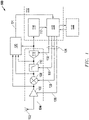
- FIG. 1 is a block diagram of an example embodiment for a receiver 100.
- the receiver includes a receive (RX) front-end 104, a power level detector 120, a processing unit 114, and memory 122.
- the amplifier 106 such as a low noise amplifier (LNA), within the RX front-end 104 is connected to an antenna 102 to receive RF signals.
- the RF signals can include signals with frequencies of hundreds of Hertz (Hz) to five Giga-Hertz (GHz) and above.
- the RX front-end 104 will typically also receive undesired interferers.
- the RX front-end 104 also includes a mixer 108, a filter 110, and an analog-to-digital converter (ADC) 112.
- the amplifier 106 receives the RF signals and outputs an amplified RF signal to the mixer 108.
- the mixer 108 down-converts the amplified RF signal from the amplifier 106 down to a lower frequency.
- the filter 110 which can be a low-pass filter, receives the down-converted RF signal and passes a filtered signal to the ADC 112.
- the ADC 112 converts the down-converted and filtered RF input signal to digital signals that are provided to the processing unit 114.
- the processing unit 114 includes frame acquisition logic 116 and an automatic gain controller (AGC) 118.
- AGC automatic gain controller
- One or more of the circuits within the RX front-end 104 can be a variable gain circuit and receive gain settings 124 from the AGC 118.
- the gain settings 124 from the AGC 118 include an amplifier gain setting 126 applied to the amplifier 106, a mixer gain setting 128 applied to the mixer 108, a filter gain setting 130 applied to the filter 110, and an ADC gain setting 132 applied to the ADC 112.
- one of these gain settings 124, all of these gain settings 124, and/or a subset of these gain settings 124 can be implemented for a particular receiver. Further, different or additional gain settings can also be used while still taking advantage of the techniques described herein.
- the AGC 118 provides gain settings 124 to one or more of the circuits within the RX front-end 104 to control their variable gain(s).
- the AGC 118 receives a power level indicator 121 from the power level detector 120. While individual gain settings 126/128/130/132 are shown being provided to each of the circuits within the RX front-end 104 (e.g., LNA 106, mixer 108, filter 110, ADC 112), it is understood that different embodiments can be implemented where only one, all, or a subset of the circuits within the RX front-end 104 receive control signals form the AGC 118.
- the power level detector 120 is shown as receiving the outputs of the LNA 106, mixer 108, filter 110, and ADC 112, it is understood that different embodiments can be implemented where the power level detector 120 receives outputs from only one, all, or a subset of the circuits within the RX front-end 104.
- the power level detector 120 is coupled only to the output of the LNA 106, and the AGC 118 adjusts only the gain setting 126 for the LNA 106.
- the power level detector 120 is coupled to the output of a plurality of the circuits in the RX front-end 104 that have variable gains, and the AGC 118 independently adjusts gain settings for each of these variable-gain circuits.
- the AGC 118 is also coupled to frame acquisition logic 116.
- the frame acquisition logic 116 receives the digital signals output by the ADC 112, and the frame acquisition logic 116 outputs control signals such as synchronization indicator 117 to the AGC 118.
- the AGC 118 is coupled to memory 122 to store and retrieve gain settings as described in more detail below. Other variations can also be implemented.
- the RF input signals will include data frames, and these data frames can include a preamble, a start-of-frame, a data payload, and/or other fields or components.
- the frame acquisition logic 116 operates to detect different portions of received data frames as well as to provide the frame synchronization indicator 117 to the AGC 118.
- the data frames are formed according to wireless communication standards such as various data frame formats provided by the IEEE 802.11 protocol (e.g., 802.11 a/b/g/n/ac) or the IEEE 802.15.4 protocol.
- the exemplary embodiment described below is based on the IEEE 802.15.4 data frame format that includes a preamble, a start of frame, and a payload, the disclosed embodiments can be used with other data frame formats.
- FIG. 2 is a block diagram of an example embodiment 200 including example internal controllers and related logic for the AGC 118.
- the AGC 118 includes gain controller 202, gain-setting capture controller 204, gain range determination logic 206, and gain setting logic 208.
- the AGC 118 stores gain settings during a sliding time window and determines a restricted gain range including an upper limit based on gain setting information identified and stored during this time window.
- FIGS. 3-7 provide example determination methods and timing diagrams according to the disclosed embodiments.
- processing unit 114 including the AGC 118 and its components can be implemented using one or more programmable circuits that are programmed to perform the functions, tasks, methods, actions, and/or other operational features described herein.
- memory 122 can be implemented using one or more non-transitory tangible computer-readable mediums.
- the gain setting logic 208 provides gain settings 124 to set the gain of one or more of the circuits within the RX front-end 104 (e.g., LNA 106, mixer 108, filter 110, and/or ADC 112).
- the gain(s) are set to a maximum value possible in response to the power level indicator 121 from the power level detector 120 without causing saturation within the RX front-end 104.
- the gain controller 202 allows the gain setting logic 208 to adjust these gains within a first range (e.g., full gain range) when the receiver is outside of data frame reception periods.
- the gain adjustments are then adjusted within a second range (e.g. , restricted gain range) when within preamble reception periods.
- the second range which can provided a restricted gain range, can be bounded by an upper limit that is determined by the gain range determination logic 206.
- the gain range determination logic 206 has two modes of operation. A first mode is an interferer tracking mode, and a second mode is a preamble gain adjustment mode.
- the gain controller 202 uses the mode signal 210 to set the operational mode in response to the synchronization indicator 117 received from the frame acquisition logic 116.
- the interferer tracking mode first mode
- the full gain range of the receiver gain stage(s) is made possible to the gain setting logic 208.
- the preamble gain adjustment mode (second mode) is selected. In this second mode, a restricted gain range is applied to the gain setting logic 208.
- the restricted gain range is determined by gain range determination logic 206 based on the gain setting history stored in the memory 122. As described further below, various methods can be performed by the gain range determination logic 206 to determine the restricted gain range. FIGS. 3-4 discussed below provide an example method and an example timing diagram, respectively, for the operation of these two modes as described with respect to FIG. 2 .
- the gain controller 202 enables the storage of gain settings into the memory 122 by the gain-setting capture controller 204 during the interferer tracking mode (first mode). A sliding time window is applied for this data capture based upon the capture window 212 as controlled by the gain controller 202.
- Gain settings 124 output from the gain setting logic 208 to the gain component(s) within the RX front-end 104 are stored in this sliding time window by having the most recent gain setting(s) replace the least recent gain setting(s) when the memory 122 is entirely filled with data.
- FIG. 3 is process flow diagram of an example embodiment 300 where gain settings are adjusted for one or more circuits within the RX front-end for a receiver according to the techniques described herein.
- a determination is made whether the receiver is outside a data reception period. If "YES,” then flow passes to block 304 wherein signal strength is monitored at regular intervals. For example, the receiver can wake up at regular time intervals from a power saving mode to monitor the received signal strength using a power level detector 120.
- gain settings for one or more of the circuits within the RX front-end 104 are adjusted using the gain settings 124 to provide increased and preferably an optimum level of sensitivity while avoiding saturation.
- the gain settings 124 are stored in the memory 122 throughout a sliding time window with a predefined duration.
- a restricted gain range is determined based upon the stored gain settings stored within the sliding time window. For example, an upper limit for a restricted gain range can be computed based on the gain settings recorded within the sliding time window. Flow then passes back to determination block 302.
- the gain adjustments in block 306 are preferably performed using a first gain range, which preferably represents the full or maximum possible gain range for the gain settings. It if further noted that monitoring in block 304 can be performed by waking the receiver up from sleep mode at regular intervals and performing the signal strength detection during these wake-up times. It is also noted that to further save power, the wake-up time interval is preferably adjusted dynamically depending on a detected frequency of interferer occurrences. For example, if the signal strength detection during wake-up times shows that the occurrence of interferes is less frequent, than the wake-up time interval can be increased. If the signal strength detection during wake-up times shows that the occurrence of interferes is more frequent, than the wake-up time interval can be decreased.
- an adjustment is made to gain level(s) within a second gain range that is set by the restricted gain range determined in block 310.
- the second gain range is a restricted version of the first gain range. Further, this gain adjustment preferably sets the gain level(s) to an optimum gain level for sensitivity while avoiding saturation. It is again noted that gain levels are adjusted by providing gain settings 124 to one or more of the circuits within the RX front-end 104.
- block 318 is reached where gain adjustments are frozen during a payload reception period.
- the restricted gain range is adjusted if a saturation threshold level is exceeded. For example, the upper limit of the restricted gain range (second gain range) can be decreased for the next data frame. Flow then passes back to determination block 320 until the payload reception has completed.
- interferer tracking operations as well as the storing of gain settings within the sliding time window can be temporarily suspended when a co-located communication device indicates that it is transmitting data. The interferer and gain level tracking is then resumed the once the co-located communication device indicates the end of data transmission to the receiver. It is further noted that different and/or additional process steps can also be used with respect to embodiment 300 while still taking advantage of the techniques described herein.
- FIG. 4 is a timing diagram of an example embodiment 400 where interferers and gain settings 124 for a receiver are tracked and stored within a sliding time window (T SLIDE ) 402.
- signal line 408 represents communications from a communication partner device to the receiver where data frames 415 are communicated to the receiver within communication phases 406.
- the data frames 415 include a reception period for a preamble 416, a reception period for a start of frame (SoF) 418, and a reception period for a payload 420.
- SoF start of frame
- the receiver enters its interferer tracking phase 404.
- gain settings 124 from the AGC 118 are detected at tracking points 410 and stored in the memory 122.
- the gain settings 126 for the LNA 106, the gain settings 128 for the mixer 108, the gain settings 130 for the filter 110, and/or the gain settings 132 for the ADC 112 can be stored for each tracking point 410.
- the interval between the tracking points can be adjusted. For example, a smaller interval 412 can be used where a higher frequency of interferers is expected, and a larger interval 414 can be sued where a smaller frequency of interferers is expected.
- the data shown as stored in memory 122 for embodiment 400 is representative only.
- the receiver does not stay continuously in an active reception mode but enters sleep or low power modes between data communications. For example, once a data exchange is completed, the receiver enters a power saving mode until the next data exchange.
- BT Bluetooth
- Zigbee devices e.g., sensors
- the data transmission occurs at regular time intervals as defined in the device profile.
- the receiver is configured to wake-up briefly at one or more points to perform the interferer tracking operations and collect data as shown for example in FIG. 4 .
- a counter is used to trigger the receiver wake-up for interferer tracking at regular intervals, and the timing for the regular intervals can be adjusted based upon the expected frequency of interferers as described herein.
- the AGC 118 adjusts the gain settings 124 for one or more of the circuits within the RX front-end 104 in response to the power level indicator 121 that is output by the power level detector 120.
- the power level indicator 121 is indicative of the signal level or strength of the received signal.
- the power level detector 120 compares the level of the signal from one or more points within the RX front-end 104 with a predefined saturation threshold and asserts a logic TRUE if the signal level is above the threshold. Otherwise, a logic FALSE is asserted.
- the AGC 118 monitors the power level indicator 121, progressively decreases the gain when a logic TRUE is received, and progressively increases the gain when a logic FALSE is received.
- the gain adjustments are made using a first gain range, such as the full gain range as permitted by the receiver.
- the gain settings 124 detected at each interferer tracking point 410 are stored into a memory 122.
- the interferer tracking phase 404 ends at the end of the sliding time window 402.
- the memory 122 can include a set of registers, a RAM (random access memory), a programmable ROM (read-only memory), non-volatile memory, and/or any suitable memory type that can store the gain settings 124.
- the size of the memory corresponds to an array of M x N, where M is the number of gain stages ( e.g. , 1 to 4 for RX front-end 104) and N is the number of tracking points within the sliding time window 402 where the gain settings are being captured.
- M is the number of gain stages (e.g. , 1 to 4 for RX front-end 104)
- N is the number of tracking points within the sliding time window 402 where the gain settings are being captured.
- the number of interferer tracking points 410 can be statically controlled where a constant time interval is used between any two tracking points 410 or can be dynamically controlled where the time interval between two tracking points 410 is adjusted over time.
- Dynamic control allows a good balance between power consumption and accurate tracking.
- the time interval between the interferer tracking points 410 can be reduced to increase the number of tracking points and thereby enhance the tracking accuracy.
- the receiver may increase the time interval between the interferer tracking points 410 to save power.
- An interferer during the interferer tracking phase 404 can be determined to have been received where a relatively low gain setting is recorded.
- a gain threshold can be used as a trigger level to indicate the receipt of an interferer during the interferer tracking phase 404. If the gain level 124 is set below this threshold level, then it can be assumed that an interferer signal has been received. If the gain level 124 is set above this threshold level, then it can be assumed that an interferer was not received. A count of interferes can then be kept during the sliding time window 402. Further, if a saturation threshold is exceeded during reception periods for the payloads 420, then an interferer can also be determined to have been received and the count can be incremented accordingly.
- the level of interferer will likely be extremely high whenever one of the co-located communication devices transmit data due to the proximity of the antennae. Recording the presence of such interferers is to be avoided as this can lead to unnecessary reductions in receiver sensitivity based upon the techniques described herein.
- these co-located communication devices are in the same system and likely controlled by a common controller and/or controllers that communicate with each other, exact moments where co-located data transmission are performed by one of these co-located transmission devices can be indicated.
- such an indication can be generated by the controller for the co-located device, a common controller, and/or some other technique through a collaborative coexistence arbitration mechanism.
- a receiver implementing the techniques described herein can suspend the interferer tracking operation until such indicator is de-asserted.
- interferer related gain settings are not stored.
- FIGS. 5 and 6 provide example embodiments that set limits for the restricted gain range used.
- the receiver when a preamble 416 is detected, the receiver enters a gain adjustment phase 514.
- the gain controller 202 adjusts the receiver gain during this preamble reception period in response to the power level detector 120 similar to gain changes during the interferer tracking phase 404, except that a restricted gain range is used instead of the full gain range.
- An upper limit for this restricted gain range is computed based on the gain settings 124 recorded during the sliding time window 402. It is noted that FIGS. 5 and 6 are just example embodiments and different techniques could also be applied to determine the restricted gain range and related limits.
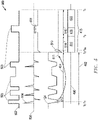
- FIG. 5 an example embodiment 500 is shown where a minimum gain setting recorded during a sliding time window (T SLIDE ) 402 is used to set limits for the restricted gain range.
- the minimum gain setting 510 is recorded at time T1 during the sliding time window 402 and is used to set the restricted upper limit 511 for the gain adjustment phase 514.
- the gain for the receiver is increased as the input signal is low at time T2 and stops at the restricted upper limit 511 at time T2a although the signal level is still below the power level detection threshold 506.
- the receiver is then prepared to handle the highest of the interferers 503 as detected during the latest sliding time window 402.
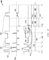
- FIG. 6 is an example embodiment 600 of a timing diagram where a recurring interferer with a likelihood of occurrence above a selected threshold is detected and used to set limits for the restricted gain range.
- a threshold of three occurrences within the sliding time window (T SLIDE ) 402 is used for this example embodiment.
- the minimum gain setting 510 is again recorded at time T 1 during the sliding time window 402 but is not used to set limits for the restricted gain range because that gain level only occurred once during the sliding time window 402.
- the lowest gain setting with an occurrence above a predefined occurrence value e.g.
- three) is the gain setting associated with low gain settings 606, 608, and 610, which are recorded at times T1a, T1b and T1c during the sliding time window 402.
- This gain level is used to set the restricted upper limit 611 for the gain adjustment phase 514.
- the gain for the receiver is increased as the input signal is low at time T2 and stops at the restricted upper limit 611 at time T2a although the signal level is still below the power level detection threshold 506.
- the receiver is then prepared to handle the recurring interferers within interferers 503 as detected during the latest sliding time window 402. No further gain increase is made after time T2a even though the signal level is below saturation level due to the restricted gain range and related upper limit.
- an interferer 503 occurring during the gain-freeze phase 516 between time T3 and time T4 does not cause saturation as indicated by gain increase 508 due to the restricted gain range and related upper limit.
- a full gain range is used for the gain settings 124 to provide the amplified signal 504 and to make adjustments based upon interferers 503 received during this interferer tracking phase 404.
- the gain settings 124 for the receiver can also be recorded during or at the end of the gain adjustment phase 514 and stored in memory 122 along with other stored gain settings.
- This additional technique effectively adds the gain adjustment phase 514 to the sliding time window 402.
- the gain controller 202 can also dynamically include or exclude the gain adjustment phase 514 during the preamble 416 from the sliding time window 402 in response to the particular data frame reception protocol being used.
- interferer resilience is improved by monitoring the output of the power level detector 120 during the gain-freeze phase 516 for reception of the data payload. If the power level detector 120 indicates an excessively high signal level during this data payload period, the upper limit of the restricted gain range can be further decreased for the reception of the next data frame 415.
- Other variations can also be implemented while still taking advantage of the techniques described herein.
- a receiver including a RX front-end, a power level detector, and an AGC.
- the RX front-end includes one or more circuits having variable gains based upon gain settings, and the RX front-end has radio frequency (RF) signals as inputs and digital signals as outputs.
- the power level detector is coupled to receive inputs from the RX front-end and has a power level indicator as an output.
- the AGC is coupled to receive the power level indicator and has the gain settings as an output to the one or more circuits within the RX front-end.
- the AGC is also configured to adjust the gain settings within a first gain range when the RF signals do not include data frames and to adjust the gain settings within a second gain range when the RF signals include data frames.
- the second gain range is a restricted version of the first gain range.
- the one or more circuits include at least one of an amplifier, a mixer, a filter, and an analog-to-digital converter.
- the data frames include data frames according to at least one of the IEEE (Institute of Electrical and Electronics Engineers) 802.11 protocol or the IEEE 802.15.4 protocol.
- the second gain range is used for gain adjustments only when a preamble for each data frame is received, and no gain adjustments are used when a payload for each data frame is received.
- the AGC is further configured to detect and store gain settings within a sliding time window during a time when the RF signals do not include data frames and to use the stored gain settings to determine the second gain range. In further embodiments, the AGC is configured to detect and store the gain settings within the sliding time window at adjustable intervals.
- the second gain range is based upon a lowest gain setting recorded within the sliding time window, and the lowest gain setting represents a largest interferer received during the sliding time window. In other additional embodiments, the second gain range is based upon a recurring lowest gain setting recorded within the sliding time window, and the recurring lowest gain setting is a lowest gain setting occurring more than a threshold number of times within the sliding time window.
- the AGC is further configured to store gain settings during preamble reception for data frames. In further embodiments, the AGC is further configured not to detect and store gain settings when a co-located communication device is indicated.
- a method including receiving radio frequency (RF) signals as inputs and outputting digital signals using a receive (RX) front-end comprising one or more circuits having variable gains based upon gain settings.
- the method also includes detecting power level for the RF signals within the RX front-end and generating a power level indicator and adjusting the gain settings for the one or more circuits based upon the power level indicator.
- the adjusting also includes adjusting the gain settings within a first gain range based upon the power level indicator when the RF signals do not include data frames and adjusting the gain settings within a second gain range when the RF signals include data frames, the second gain range being a restricted version of the first gain range.
- the one or more circuits include at least one of an amplifier, a mixer, a filter, and an analog-to-digital converter.
- the data frames include data frames according to at least one of the IEEE (Institute of Electrical and Electronics Engineers) 802.11 protocol or the IEEE 802.15.4 protocol.
- the method includes adjusting the gain settings using the second gain range only when a preamble for each data frame is received, and not adjusting the gain settings when a payload for each data frame is received.
- the method includes detecting gain settings within a sliding time window during a time when the RF signals do not include data frames, storing the detected gain settings, and using the stored gain settings to determine the second gain range. In further embodiments, the method includes detecting and storing the gain settings within the sliding time window at adjustable intervals.
- the second gain range is based upon a lowest gain setting recorded within the sliding time window, and the lowest gain setting represents a largest interferer received during the sliding time window. In other additional embodiments, the second gain range is based upon a recurring lowest gain setting recorded within the sliding time window, and the recurring lowest gain setting is a lowest gain setting occurring more than a threshold number of times within the sliding time window.
- the method includes storing gain settings during preamble reception for data frames. In further embodiments, the method includes suspending the detection and storing of the gain settings when a co-located communication device is indicated.
- the functional blocks, components, systems, devices, and/or circuitry described herein such as the RX front-end 104 (including the LNA 106, the mixer 108, the filter 110, and the ADC 112 as well as their component parts) and the processing unit 114 (including the frame acquisition logic 116 and the AGC 118 as well as their component parts) can be implemented using hardware, software, or a combination of hardware and software.
- the disclosed embodiments can be implemented using one or more programmable circuits that are programmed to perform the functions, tasks, methods, actions, and/or other operational features described herein for the disclosed embodiments.
- the one or more programmable circuits can include, for example, one or more processors and/or configurable logic devices (CLDs).
- the one or more processors can be, for example, one or more central processing units (CPUs), controllers, microcontrollers, microprocessors, hardware accelerators, ASICs (application specific integrated circuit), and/or other integrated processing devices.
- the one or more CLDs can be, for example, one or more CPLDs (complex programmable logic devices), FPGAs (field programmable gate arrays), PLAs (programmable logic array), reconfigurable logic circuits, and/or other integrated logic devices.
- the programmable circuits including the one or more processors, can be programmed to execute software, firmware, code, and/or other program instructions that are embodied in one or more non-transitory tangible computer-readable mediums to perform the functions, tasks, methods, actions, and/or other operational features described herein for the disclosed embodiments.
- the programmable circuits, including the one or more CLDs can also be programmed using logic code, logic definitions, hardware description languages, configuration files, and/or other logic instructions that are embodied in one or more non-transitory tangible computer-readable mediums to perform the functions, tasks, methods, actions, and/or other operational features described herein for the disclosed embodiments.
- the one or more non-transitory tangible computer-readable mediums can include, for example, one or more data storage devices, memory devices, flash memories, random access memories, read only memories, programmable memory devices, reprogrammable storage devices, hard drives, floppy disks, DVDs, CD-ROMs, and/or any other non-transitory tangible computer-readable mediums.
- Other variations can also be implemented while still taking advantage of the techniques described herein.
Landscapes
- Engineering & Computer Science (AREA)
- Computer Networks & Wireless Communication (AREA)
- Signal Processing (AREA)
- Quality & Reliability (AREA)
- Physics & Mathematics (AREA)
- Electromagnetism (AREA)
- Circuits Of Receivers In General (AREA)
- Control Of Amplification And Gain Control (AREA)
Description
- This technical field relates to receiving radio frequency (RF) transmissions and, more particularly, to countering interfering signals present during the reception of RF transmissions.
- Increasing numbers and types of devices are becoming portable and non-portable wireless devices. The proliferation of portable connected devices such as mobile phones, laptops, smart watches, tablets etc. as well as non-portable connected devices such as televisions, video game consoles, appliances, etc. have saturated many environments with radio frequency (RF) signals. Due to this proliferation of RF signals, connected devices receive many unwanted signals, called interferers, in addition to receiving desired RF signals from communication partner device(s). The interferers can occur in a random and unpredictable manner. For example, interferers can occur in the form of signal bursts of variable duration and have signal strengths possibly much higher than the desired signal at the receiving device. Interferers with a high signal strength can cause saturation of the receive circuitry thereby preventing proper reception of the desired data.
- Many prior solutions have addressed this interferer issue by continuously monitoring the received signal strength and immediately adjusting amplifier gains to avoid saturation while still maintaining sensitivity levels for the receiving device. However, when operating within popular wireless communication protocols such as IEEE (Institute of Electrical and Electronics Engineers) 802.11 protocols for Wireless Personal Area Networks (e.g., WiFi) or IEEE 802.15.4 protocols for Wireless Personal Area Networks (e.g., Bluetooth, Zigbee), the receiver is often not allowed by these protocols to adjust gain during reception of the data payload. Due to these limitations, prior receiver solutions for these communication protocols adjust the gain during a time interval prior to the payload reception. This gain adjustment is typically based upon the real-time received signal, and the gain adjustment is fixed just before switching to the payload reception period. The inability to perform gain adjustments during payload reception, however, can cause degradation in receiver performance. For example, due to their random nature in occurrence and strength level, interferers may appear during payload reception and cause saturation of the receive circuity resulting in data loss due the inability to adjust the fixed gain settings set prior to the payload reception period.
US 2015/222373 A1 describes an automatic gain control apparatus and method in wireless telecommunication system based on time division duplex. - The invention is described by the content of the independent claims.
- It is noted that the appended figures illustrate only example embodiments and are, therefore, not to be considered as limiting the scope of the present invention. Elements in the figures are illustrated for simplicity and clarity and have not necessarily been drawn to scale.
-
FIG. 1 is a block diagram of an example embodiment for a receiver including an automatic gain controller (AGC) according to the disclosed embodiments. -
FIG. 2 is a block diagram of an example embodiment including example internal controllers and related logic for an AGC according to the disclosed embodiments. -
FIG. 3 is process flow diagram of an example embodiment where gain settings are adjusted for one or more circuits within a receive (RX) front-end for a receiver within an interferer tracking phase using a first gain range and a within a payload reception phase using a restricted gain range. -
FIG. 4 is a timing diagram of an example embodiment where interferers and gain settings for a receiver are tracked and stored within a sliding time window. -
FIG. 5 is a timing diagram of an example embodiment where a minimum gain setting recorded during a sliding time window is used to set limits for the restricted gain range used for payload reception. -
FIG. 6 is an example embodiment of a timing diagram where a recurring interferer with a likelihood of occurrence above a selected threshold is detected and used to set limits for the restricted gain range for payload reception. - Wireless receivers and related methods with interferer immunity are disclosed. The disclosed embodiments determine variable gain settings for reception of radio frequency (RF) signals based upon past information on detected interferers thereby allowing receiver gain settings to achieve improved and/or optimum trade-offs between reception sensitivity and random interferer immunity. For example, past information for the signal strength of interferers is considered to control the actual gain adjustment for variable gain circuits including amplifiers within a receiver. For receivers operating within protocols that do not allow gain adjustments during payload reception such as the IEEE 802.11 protocol and the 802.15.4 protocol, the disclosed techniques allow receivers to have higher immunity to interferers even if the interferers occur during the gain-frozen payload reception period while still maintaining adequate and preferably optimum sensitivity levels. A variety of additional and/or different features and variations can also be implemented.
- For one embodiment according to the invention, gain settings for variable gain circuits within a receive (RX) front-end are determined and stored at regular time points during a sliding time window when the receiver is not receiving a data payload. These gain settings can be assumed to correspond to the presence or lack of interferers being received by the receiver during this sliding time window. For example, a low gain setting is indicates that an interferer has been received, while a high gain setting indicates that interferers are likely not present. Based upon the gain settings for prior interferers within the sliding time window, a restricted gain range is determined and later applied for a gain adjustment phase during reception of the preamble for a data frame. The receiver thereby determines the most appropriate gain levels for the restricted gain range based upon past interferers and applies this gain range as a control input for gain adjustment during the preamble phase before the gain-freeze period during data payload reception. The past interferer information improves the possibility of capturing and identifying the most likely worst-case and/or recurring interferers a receiver will likely experience during reception of data frames and makes the overall system more robust against interferers that may occur during data payload reception. The sliding time window allows the receiver to adapt to the actual environmental conditions, and the receiver can be continually adjusted to have an increased or preferably optimum sensitivity level while still maintaining adequate immunity to interferers. For certain embodiments, the receiver wakes up from a power saving mode to perform interferer tracking, and the time intervals between tracking points for detecting the gain settings can be dynamically controlled, for example, based upon the expected frequency of interferers. Further, the receiver can suspend the interferer tracking operation based on indication of a co-located communication device that may communicate with other devices as such co-located communication devices can lead to unneeded gain limits. Additional and/or different features can also be provided while still taking advantage of the techniques described herein.
-
FIG. 1 is a block diagram of an example embodiment for areceiver 100. The receiver includes a receive (RX) front-end 104, apower level detector 120, aprocessing unit 114, andmemory 122. Theamplifier 106, such as a low noise amplifier (LNA), within the RX front-end 104 is connected to anantenna 102 to receive RF signals. The RF signals can include signals with frequencies of hundreds of Hertz (Hz) to five Giga-Hertz (GHz) and above. In addition to receiving desired RF signals that include data frames communicated from communication partner devices, the RX front-end 104 will typically also receive undesired interferers. In addition to theamplifier 106, the RX front-end 104 also includes amixer 108, afilter 110, and an analog-to-digital converter (ADC) 112. Theamplifier 106 receives the RF signals and outputs an amplified RF signal to themixer 108. Themixer 108 down-converts the amplified RF signal from theamplifier 106 down to a lower frequency. Thefilter 110, which can be a low-pass filter, receives the down-converted RF signal and passes a filtered signal to theADC 112. TheADC 112 converts the down-converted and filtered RF input signal to digital signals that are provided to theprocessing unit 114. - For the
embodiment 100 depicted, theprocessing unit 114 includesframe acquisition logic 116 and an automatic gain controller (AGC) 118. One or more of the circuits within the RX front-end 104 can be a variable gain circuit and receivegain settings 124 from the AGC 118. For theembodiment 100 depicted, thegain settings 124 from theAGC 118 include anamplifier gain setting 126 applied to theamplifier 106, amixer gain setting 128 applied to themixer 108, afilter gain setting 130 applied to thefilter 110, and anADC gain setting 132 applied to theADC 112. As described in more detail below, one of thesegain settings 124, all of thesegain settings 124, and/or a subset of thesegain settings 124 can be implemented for a particular receiver. Further, different or additional gain settings can also be used while still taking advantage of the techniques described herein. - In operation, the AGC 118 provides
gain settings 124 to one or more of the circuits within the RX front-end 104 to control their variable gain(s). The AGC 118 receives apower level indicator 121 from thepower level detector 120. Whileindividual gain settings 126/128/130/132 are shown being provided to each of the circuits within the RX front-end 104 (e.g., LNA 106,mixer 108,filter 110, ADC 112), it is understood that different embodiments can be implemented where only one, all, or a subset of the circuits within the RX front-end 104 receive control signals form theAGC 118. Similarly, while thepower level detector 120 is shown as receiving the outputs of the LNA 106,mixer 108,filter 110, and ADC 112, it is understood that different embodiments can be implemented where thepower level detector 120 receives outputs from only one, all, or a subset of the circuits within the RX front-end 104. For one example embodiment, thepower level detector 120 is coupled only to the output of the LNA 106, and the AGC 118 adjusts only thegain setting 126 for the LNA 106. In another example embodiment, thepower level detector 120 is coupled to the output of a plurality of the circuits in the RX front-end 104 that have variable gains, and theAGC 118 independently adjusts gain settings for each of these variable-gain circuits. The AGC 118 is also coupled toframe acquisition logic 116. Theframe acquisition logic 116 receives the digital signals output by theADC 112, and theframe acquisition logic 116 outputs control signals such assynchronization indicator 117 to the AGC 118. TheAGC 118 is coupled tomemory 122 to store and retrieve gain settings as described in more detail below. Other variations can also be implemented. - For many communication protocols, the RF input signals will include data frames, and these data frames can include a preamble, a start-of-frame, a data payload, and/or other fields or components. For one embodiment, the
frame acquisition logic 116 operates to detect different portions of received data frames as well as to provide theframe synchronization indicator 117 to theAGC 118. For some embodiments, the data frames are formed according to wireless communication standards such as various data frame formats provided by the IEEE 802.11 protocol (e.g., 802.11 a/b/g/n/ac) or the IEEE 802.15.4 protocol. Although the exemplary embodiment described below is based on the IEEE 802.15.4 data frame format that includes a preamble, a start of frame, and a payload, the disclosed embodiments can be used with other data frame formats. -
FIG. 2 is a block diagram of anexample embodiment 200 including example internal controllers and related logic for theAGC 118. For theexample embodiment 200, theAGC 118 includesgain controller 202, gain-settingcapture controller 204, gainrange determination logic 206, and gain settinglogic 208. As described herein, theAGC 118 stores gain settings during a sliding time window and determines a restricted gain range including an upper limit based on gain setting information identified and stored during this time window. Various determination methods for the gain range and upper limit can be applied depending on the interferer types. FIGS. 3-7 provide example determination methods and timing diagrams according to the disclosed embodiments. Further, it is noted that theprocessing unit 114 including theAGC 118 and its components can be implemented using one or more programmable circuits that are programmed to perform the functions, tasks, methods, actions, and/or other operational features described herein. It is further noted that thememory 122 can be implemented using one or more non-transitory tangible computer-readable mediums. - In operation, the
gain setting logic 208 providesgain settings 124 to set the gain of one or more of the circuits within the RX front-end 104 (e.g.,LNA 106,mixer 108,filter 110, and/or ADC 112). Preferably, the gain(s) are set to a maximum value possible in response to thepower level indicator 121 from thepower level detector 120 without causing saturation within the RX front-end 104. Thegain controller 202 allows thegain setting logic 208 to adjust these gains within a first range (e.g., full gain range) when the receiver is outside of data frame reception periods. The gain adjustments are then adjusted within a second range (e.g., restricted gain range) when within preamble reception periods. For example, the second range, which can provided a restricted gain range, can be bounded by an upper limit that is determined by the gainrange determination logic 206. - The gain
range determination logic 206 has two modes of operation. A first mode is an interferer tracking mode, and a second mode is a preamble gain adjustment mode. Thegain controller 202 uses themode signal 210 to set the operational mode in response to thesynchronization indicator 117 received from theframe acquisition logic 116. When no communication packet is being received, the interferer tracking mode (first mode) is selected. In the first mode, the full gain range of the receiver gain stage(s) is made possible to thegain setting logic 208. During the reception of the packet preamble, the preamble gain adjustment mode (second mode) is selected. In this second mode, a restricted gain range is applied to thegain setting logic 208. The restricted gain range is determined by gainrange determination logic 206 based on the gain setting history stored in thememory 122. As described further below, various methods can be performed by the gainrange determination logic 206 to determine the restricted gain range.FIGS. 3-4 discussed below provide an example method and an example timing diagram, respectively, for the operation of these two modes as described with respect toFIG. 2 . - The
gain controller 202 enables the storage of gain settings into thememory 122 by the gain-settingcapture controller 204 during the interferer tracking mode (first mode). A sliding time window is applied for this data capture based upon thecapture window 212 as controlled by thegain controller 202.Gain settings 124 output from thegain setting logic 208 to the gain component(s) within the RX front-end 104 are stored in this sliding time window by having the most recent gain setting(s) replace the least recent gain setting(s) when thememory 122 is entirely filled with data. -
FIG. 3 is process flow diagram of anexample embodiment 300 where gain settings are adjusted for one or more circuits within the RX front-end for a receiver according to the techniques described herein. Inblock 302, a determination is made whether the receiver is outside a data reception period. If "YES," then flow passes to block 304 wherein signal strength is monitored at regular intervals. For example, the receiver can wake up at regular time intervals from a power saving mode to monitor the received signal strength using apower level detector 120. Inblock 306, gain settings for one or more of the circuits within the RX front-end 104 are adjusted using thegain settings 124 to provide increased and preferably an optimum level of sensitivity while avoiding saturation. Inblock 308, thegain settings 124 are stored in thememory 122 throughout a sliding time window with a predefined duration. Inblock 310, a restricted gain range is determined based upon the stored gain settings stored within the sliding time window. For example, an upper limit for a restricted gain range can be computed based on the gain settings recorded within the sliding time window. Flow then passes back to determination block 302. - It is noted that the gain adjustments in
block 306 are preferably performed using a first gain range, which preferably represents the full or maximum possible gain range for the gain settings. It if further noted that monitoring inblock 304 can be performed by waking the receiver up from sleep mode at regular intervals and performing the signal strength detection during these wake-up times. It is also noted that to further save power, the wake-up time interval is preferably adjusted dynamically depending on a detected frequency of interferer occurrences. For example, if the signal strength detection during wake-up times shows that the occurrence of interferes is less frequent, than the wake-up time interval can be increased. If the signal strength detection during wake-up times shows that the occurrence of interferes is more frequent, than the wake-up time interval can be decreased. - In the determination in
block 302 is "NO," then the receiver a data reception period and block 312 is reached. Inblock 312, a determination is made whether the data reception is within a preamble period preceding a data payload period. If "YES," then flow passes to block 314 where signal strength is determined. Inblock 316, during the preamble period preceding the data payload period, an adjustment is made to gain level(s) within a second gain range that is set by the restricted gain range determined inblock 310. The second gain range is a restricted version of the first gain range. Further, this gain adjustment preferably sets the gain level(s) to an optimum gain level for sensitivity while avoiding saturation. It is again noted that gain levels are adjusted by providinggain settings 124 to one or more of the circuits within the RX front-end 104. - If the determination in
block 312 is "NO," then block 318 is reached where gain adjustments are frozen during a payload reception period. Flow then passes to block 320 where a determination is made whether the payload reception has completed. If "YES," then flow passes back to block 302. If "NO," then flow passes to block 322 where the signal strength is again detected. Inblock 324, the restricted gain range is adjusted if a saturation threshold level is exceeded. For example, the upper limit of the restricted gain range (second gain range) can be decreased for the next data frame. Flow then passes back to determination block 320 until the payload reception has completed. - Although not shown in
example embodiment 300, it is further noted that interferer tracking operations as well as the storing of gain settings within the sliding time window can be temporarily suspended when a co-located communication device indicates that it is transmitting data. The interferer and gain level tracking is then resumed the once the co-located communication device indicates the end of data transmission to the receiver. It is further noted that different and/or additional process steps can also be used with respect toembodiment 300 while still taking advantage of the techniques described herein. -
FIG. 4 is a timing diagram of anexample embodiment 400 where interferers and gainsettings 124 for a receiver are tracked and stored within a sliding time window (TSLIDE) 402. Forembodiment 400,signal line 408 represents communications from a communication partner device to the receiver where data frames 415 are communicated to the receiver within communication phases 406. The data frames 415 include a reception period for apreamble 416, a reception period for a start of frame (SoF) 418, and a reception period for apayload 420. In periods where data frames 415 are not being communicated, the receiver enters itsinterferer tracking phase 404. During these interferer tracking phases 404,gain settings 124 from theAGC 118 are detected at trackingpoints 410 and stored in thememory 122. For example, thegain settings 126 for theLNA 106, thegain settings 128 for themixer 108, thegain settings 130 for thefilter 110, and/or thegain settings 132 for theADC 112 can be stored for eachtracking point 410. As described herein, the interval between the tracking points can be adjusted. For example, asmaller interval 412 can be used where a higher frequency of interferers is expected, and alarger interval 414 can be sued where a smaller frequency of interferers is expected. It is also noted that the data shown as stored inmemory 122 forembodiment 400 is representative only. - To save power in some embodiments, the receiver does not stay continuously in an active reception mode but enters sleep or low power modes between data communications. For example, once a data exchange is completed, the receiver enters a power saving mode until the next data exchange. In the case of Bluetooth (BT) devices, the time interval between data communication events is negotiated between the paired devices. In case of Zigbee devices (e.g., sensors), the data transmission occurs at regular time intervals as defined in the device profile. Between two adjacent communication phases, the receiver is configured to wake-up briefly at one or more points to perform the interferer tracking operations and collect data as shown for example in
FIG. 4 . For one embodiment, a counter is used to trigger the receiver wake-up for interferer tracking at regular intervals, and the timing for the regular intervals can be adjusted based upon the expected frequency of interferers as described herein. - During an
interferer tracking phase 404, theAGC 118 adjusts thegain settings 124 for one or more of the circuits within the RX front-end 104 in response to thepower level indicator 121 that is output by thepower level detector 120. Thepower level indicator 121 is indicative of the signal level or strength of the received signal. For one embodiment, thepower level detector 120 compares the level of the signal from one or more points within the RX front-end 104 with a predefined saturation threshold and asserts a logic TRUE if the signal level is above the threshold. Otherwise, a logic FALSE is asserted. TheAGC 118 monitors thepower level indicator 121, progressively decreases the gain when a logic TRUE is received, and progressively increases the gain when a logic FALSE is received. During the interferetracking phase 404, the gain adjustments are made using a first gain range, such as the full gain range as permitted by the receiver. Thegain settings 124 detected at eachinterferer tracking point 410 are stored into amemory 122. Theinterferer tracking phase 404 ends at the end of the slidingtime window 402. - It is noted that the
memory 122 can include a set of registers, a RAM (random access memory), a programmable ROM (read-only memory), non-volatile memory, and/or any suitable memory type that can store thegain settings 124. The size of the memory corresponds to an array of M x N, where M is the number of gain stages (e.g., 1 to 4 for RX front-end 104) and N is the number of tracking points within the slidingtime window 402 where the gain settings are being captured. It is further noted that the number of interferer tracking points 410 can be statically controlled where a constant time interval is used between any twotracking points 410 or can be dynamically controlled where the time interval between twotracking points 410 is adjusted over time. Dynamic control allows a good balance between power consumption and accurate tracking. In case numerous interferers are observed and recorded, the time interval between the interferer tracking points 410 can be reduced to increase the number of tracking points and thereby enhance the tracking accuracy. In contrast, if a small number of interferers are observed and recorded, then the receiver may increase the time interval between the interferer tracking points 410 to save power. - An interferer during the
interferer tracking phase 404 can be determined to have been received where a relatively low gain setting is recorded. For example, a gain threshold can be used as a trigger level to indicate the receipt of an interferer during theinterferer tracking phase 404. If thegain level 124 is set below this threshold level, then it can be assumed that an interferer signal has been received. If thegain level 124 is set above this threshold level, then it can be assumed that an interferer was not received. A count of interferes can then be kept during the slidingtime window 402. Further, if a saturation threshold is exceeded during reception periods for thepayloads 420, then an interferer can also be determined to have been received and the count can be incremented accordingly. - In the case where the receiver is integrated in a larger system such as a gateway or multi-protocol router as one of several communication devices (e.g., Zigbee along with BT, WiFi, etc.), the level of interferer will likely be extremely high whenever one of the co-located communication devices transmit data due to the proximity of the antennae. Recording the presence of such interferers is to be avoided as this can lead to unnecessary reductions in receiver sensitivity based upon the techniques described herein. As these co-located communication devices are in the same system and likely controlled by a common controller and/or controllers that communicate with each other, exact moments where co-located data transmission are performed by one of these co-located transmission devices can be indicated. For example, such an indication can be generated by the controller for the co-located device, a common controller, and/or some other technique through a collaborative coexistence arbitration mechanism. When an indication of data transmission of one of the co-located communication devices is asserted, a receiver implementing the techniques described herein can suspend the interferer tracking operation until such indicator is de-asserted. When the interferer tracking operations are suspended, interferer related gain settings are not stored.
-
FIGS. 5 and6 provide example embodiments that set limits for the restricted gain range used. For these embodiments, when apreamble 416 is detected, the receiver enters again adjustment phase 514. Thegain controller 202 adjusts the receiver gain during this preamble reception period in response to thepower level detector 120 similar to gain changes during theinterferer tracking phase 404, except that a restricted gain range is used instead of the full gain range. An upper limit for this restricted gain range is computed based on thegain settings 124 recorded during the slidingtime window 402. It is noted thatFIGS. 5 and6 are just example embodiments and different techniques could also be applied to determine the restricted gain range and related limits. - Looking first to
FIG. 5 , anexample embodiment 500 is shown where a minimum gain setting recorded during a sliding time window (TSLIDE) 402 is used to set limits for the restricted gain range. For the example shown, the minimum gain setting 510 is recorded at time T1 during the slidingtime window 402 and is used to set the restrictedupper limit 511 for thegain adjustment phase 514. As shown during reception of thepreamble 416 with respect toelement 512, the gain for the receiver is increased as the input signal is low at time T2 and stops at the restrictedupper limit 511 at time T2a although the signal level is still below the powerlevel detection threshold 506. The receiver is then prepared to handle the highest of theinterferers 503 as detected during the latest slidingtime window 402. No further gain increase is made after time T2a even though the signal level is below saturation level due to the restricted gain range and related upper limit. Further, aninterferer 503 occurring during the gain-freeze phase 516 between time T3 and time T4 does not cause saturation as indicated bygain increase 508 due to the restricted gain range and related upper limit. In contrast, as shown in theinterferer tracking phase 404, a full gain range is used for thegain settings 124 to provide the amplifiedsignal 504 and to make adjustments based uponinterferers 503 received during thisinterferer tracking phase 404. -
FIG. 6 is anexample embodiment 600 of a timing diagram where a recurring interferer with a likelihood of occurrence above a selected threshold is detected and used to set limits for the restricted gain range. For example, a threshold of three occurrences within the sliding time window (TSLIDE) 402 is used for this example embodiment. For the example shown, the minimum gain setting 510 is again recorded attime T 1 during the slidingtime window 402 but is not used to set limits for the restricted gain range because that gain level only occurred once during the slidingtime window 402. The lowest gain setting with an occurrence above a predefined occurrence value (e.g., three) is the gain setting associated withlow gain settings time window 402. This gain level is used to set the restrictedupper limit 611 for thegain adjustment phase 514. As shown during the reception of thepreamble 416 with respect toelement 612, the gain for the receiver is increased as the input signal is low at time T2 and stops at the restrictedupper limit 611 at time T2a although the signal level is still below the powerlevel detection threshold 506. The receiver is then prepared to handle the recurring interferers withininterferers 503 as detected during the latest slidingtime window 402. No further gain increase is made after time T2a even though the signal level is below saturation level due to the restricted gain range and related upper limit. Further, aninterferer 503 occurring during the gain-freeze phase 516 between time T3 and time T4 does not cause saturation as indicated bygain increase 508 due to the restricted gain range and related upper limit. In contrast, as shown in theinterferer tracking phase 404, a full gain range is used for thegain settings 124 to provide the amplifiedsignal 504 and to make adjustments based uponinterferers 503 received during thisinterferer tracking phase 404. - For the embodiments disclosed herein, it is also possible that interferers may occur during the
gain adjustment phase 514 when thepreamble 416 is being received. As such, thegain settings 124 for the receiver can also be recorded during or at the end of thegain adjustment phase 514 and stored inmemory 122 along with other stored gain settings. This additional technique effectively adds thegain adjustment phase 514 to the slidingtime window 402. These additional gain tracking points can be advantageous, for example, in cases of small time intervals between data frame reception periods. Thegain controller 202 can also dynamically include or exclude thegain adjustment phase 514 during thepreamble 416 from the slidingtime window 402 in response to the particular data frame reception protocol being used. For one additional embodiment, interferer resilience is improved by monitoring the output of thepower level detector 120 during the gain-freeze phase 516 for reception of the data payload. If thepower level detector 120 indicates an excessively high signal level during this data payload period, the upper limit of the restricted gain range can be further decreased for the reception of thenext data frame 415. Other variations can also be implemented while still taking advantage of the techniques described herein. - As described herein, a variety of embodiments can be implemented and different features and variations can be implemented, as desired.
- For one embodiment, a receiver is disclosed including a RX front-end, a power level detector, and an AGC. The RX front-end includes one or more circuits having variable gains based upon gain settings, and the RX front-end has radio frequency (RF) signals as inputs and digital signals as outputs. The power level detector is coupled to receive inputs from the RX front-end and has a power level indicator as an output. The AGC is coupled to receive the power level indicator and has the gain settings as an output to the one or more circuits within the RX front-end. The AGC is also configured to adjust the gain settings within a first gain range when the RF signals do not include data frames and to adjust the gain settings within a second gain range when the RF signals include data frames. The second gain range is a restricted version of the first gain range.
- In additional embodiments, the one or more circuits include at least one of an amplifier, a mixer, a filter, and an analog-to-digital converter. In further embodiments, the data frames include data frames according to at least one of the IEEE (Institute of Electrical and Electronics Engineers) 802.11 protocol or the IEEE 802.15.4 protocol. In further embodiments, the second gain range is used for gain adjustments only when a preamble for each data frame is received, and no gain adjustments are used when a payload for each data frame is received.
- In additional embodiments, the AGC is further configured to detect and store gain settings within a sliding time window during a time when the RF signals do not include data frames and to use the stored gain settings to determine the second gain range. In further embodiments, the AGC is configured to detect and store the gain settings within the sliding time window at adjustable intervals.
- In additional embodiments, the second gain range is based upon a lowest gain setting recorded within the sliding time window, and the lowest gain setting represents a largest interferer received during the sliding time window. In other additional embodiments, the second gain range is based upon a recurring lowest gain setting recorded within the sliding time window, and the recurring lowest gain setting is a lowest gain setting occurring more than a threshold number of times within the sliding time window.
- In additional embodiments, the AGC is further configured to store gain settings during preamble reception for data frames. In further embodiments, the AGC is further configured not to detect and store gain settings when a co-located communication device is indicated.
- For one embodiment, a method is disclosed including receiving radio frequency (RF) signals as inputs and outputting digital signals using a receive (RX) front-end comprising one or more circuits having variable gains based upon gain settings. The method also includes detecting power level for the RF signals within the RX front-end and generating a power level indicator and adjusting the gain settings for the one or more circuits based upon the power level indicator. The adjusting also includes adjusting the gain settings within a first gain range based upon the power level indicator when the RF signals do not include data frames and adjusting the gain settings within a second gain range when the RF signals include data frames, the second gain range being a restricted version of the first gain range.
- In additional embodiments, the one or more circuits include at least one of an amplifier, a mixer, a filter, and an analog-to-digital converter. In further embodiments, the data frames include data frames according to at least one of the IEEE (Institute of Electrical and Electronics Engineers) 802.11 protocol or the IEEE 802.15.4 protocol.
- In additional embodiments, the method includes adjusting the gain settings using the second gain range only when a preamble for each data frame is received, and not adjusting the gain settings when a payload for each data frame is received.
- In additional embodiments, the method includes detecting gain settings within a sliding time window during a time when the RF signals do not include data frames, storing the detected gain settings, and using the stored gain settings to determine the second gain range. In further embodiments, the method includes detecting and storing the gain settings within the sliding time window at adjustable intervals.
- In additional embodiments, the second gain range is based upon a lowest gain setting recorded within the sliding time window, and the lowest gain setting represents a largest interferer received during the sliding time window. In other additional embodiments, the second gain range is based upon a recurring lowest gain setting recorded within the sliding time window, and the recurring lowest gain setting is a lowest gain setting occurring more than a threshold number of times within the sliding time window.
- In additional embodiments, the method includes storing gain settings during preamble reception for data frames. In further embodiments, the method includes suspending the detection and storing of the gain settings when a co-located communication device is indicated.
- It is further noted that the functional blocks, components, systems, devices, and/or circuitry described herein such as the RX front-end 104 (including the
LNA 106, themixer 108, thefilter 110, and theADC 112 as well as their component parts) and the processing unit 114 (including theframe acquisition logic 116 and theAGC 118 as well as their component parts) can be implemented using hardware, software, or a combination of hardware and software. For example, the disclosed embodiments can be implemented using one or more programmable circuits that are programmed to perform the functions, tasks, methods, actions, and/or other operational features described herein for the disclosed embodiments. The one or more programmable circuits can include, for example, one or more processors and/or configurable logic devices (CLDs). The one or more processors can be, for example, one or more central processing units (CPUs), controllers, microcontrollers, microprocessors, hardware accelerators, ASICs (application specific integrated circuit), and/or other integrated processing devices. The one or more CLDs can be, for example, one or more CPLDs (complex programmable logic devices), FPGAs (field programmable gate arrays), PLAs (programmable logic array), reconfigurable logic circuits, and/or other integrated logic devices. Further, the programmable circuits, including the one or more processors, can be programmed to execute software, firmware, code, and/or other program instructions that are embodied in one or more non-transitory tangible computer-readable mediums to perform the functions, tasks, methods, actions, and/or other operational features described herein for the disclosed embodiments. The programmable circuits, including the one or more CLDs, can also be programmed using logic code, logic definitions, hardware description languages, configuration files, and/or other logic instructions that are embodied in one or more non-transitory tangible computer-readable mediums to perform the functions, tasks, methods, actions, and/or other operational features described herein for the disclosed embodiments. In addition, the one or more non-transitory tangible computer-readable mediums can include, for example, one or more data storage devices, memory devices, flash memories, random access memories, read only memories, programmable memory devices, reprogrammable storage devices, hard drives, floppy disks, DVDs, CD-ROMs, and/or any other non-transitory tangible computer-readable mediums. Other variations can also be implemented while still taking advantage of the techniques described herein. - Unless stated otherwise, terms such as "first" and "second" are used to arbitrarily distinguish between the elements such terms describe. Thus, these terms are not necessarily intended to indicate temporal or other prioritization of such elements.
Claims (13)
- A receiver, comprising:a receive RX front-end (104) comprising one or more circuits having variable gains based upon gain settings, the RX front-end having radio frequency RF signals as inputs and digital signals as outputs;a power level detector (120) coupled to receive inputs from the RX front-end and having a power level indicator as an output; andan automatic gain controller, AGC(118), coupled to receive the power level indicator and having the gain settings as an output to the one or more circuits within the RX front-end;wherein the AGC is configured to adjust the gain settings within a first gain range when the RF signals do not include data frames and to adjust the gain settings within a second gain range when the RF signals include data frames; andwherein the second gain range is a restricted version of the first gain range; and wherein the AGC is further configured to detect and store gain settings within a sliding time window (402) during a time when the RF signals do not include data frames and to use the stored gain settings to determine the second gain range.
- The receiver of claim 1, wherein the one or more circuits comprise at least one of an amplifier, a mixer, a filter, and an analog-to-digital converter.
- The receiver of claim 1 or 2, wherein the data frames comprise data frames according to at least one of the IEEE (Institute of Electrical and Electronics Engineers) 802.11 protocol or the IEEE 802.15.4 protocol.
- The receiver of any preceding claim, wherein the second gain range is based upon a lowest gain setting recorded within the sliding time window, the lowest gain setting representing a largest interferer received during the sliding time window.
- The receiver of any preceding claim, wherein the second gain range is based upon a recurring lowest gain setting recorded within the sliding time window, the recurring lowest gain setting being a lowest gain setting occurring more than a threshold number of times within the sliding time window.
- The receiver of any of any preceding claim, wherein the AGC is further configured not to detect and store gain settings when a co-located communication device is indicated.
- A method, comprising:receiving radio frequency RF signals as inputs and outputting digital signals using a receive RX front-end (104) comprising one or more circuits having variable gains based upon gain settings;detecting power level for the RF signals within the RX front-end and generating a power level indicator; andadjusting the gain settings for the one or more circuits based upon the power level indicator;wherein the adjusting comprises:adjusting the gain settings within a first gain range based upon the power level indicator when the RF signals do not include data frames; andadjusting the gain settings within a second gain range when the RF signals include data frames, the second gain range being a restricted version of the first gain range;wherein the method further comprises detecting gain settings within a sliding time window (402) during a time when the RF signals do not include data frames, storing the detected gain settings, and using the stored gain settings to determine the second gain range.
- The method of claim 7, further comprising adjusting the gain settings using the second gain range only when a preamble for each data frame is received, and not adjusting the gain settings when a payload for each data frame is received.
- The method of claim 7 or 8, further comprising detecting and storing the gain settings within the sliding time window at adjustable intervals.
- The method of any of claims 7 to 9, wherein the second gain range is based upon a lowest gain setting recorded within the sliding time window, the lowest gain setting representing a largest interferer received during the sliding time window.
- The method of any of claims 7 to 10, wherein the second gain range is based upon a recurring lowest gain setting recorded within the sliding time window, the recurring lowest gain setting being a lowest gain setting occurring more than a threshold number of times within the sliding time window.
- The method of any of claims 7 to 11, further comprising storing gain settings during preamble reception for data frames.
- The method of any of claims 7 to 12, further comprising suspending detection and storing of the gain settings when a co-located communication device is indicated.
Priority Applications (3)
| Application Number | Priority Date | Filing Date | Title |
|---|---|---|---|
| EP18306543.2A EP3657672B1 (en) | 2018-11-21 | 2018-11-21 | Wireless receivers and related methods with random interferer immunity |
| US16/270,807 US10581474B1 (en) | 2018-11-21 | 2019-02-08 | Wireless receivers and related methods with random interferer immunity |
| CN201911152700.1A CN111211796B (en) | 2018-11-21 | 2019-11-21 | Wireless receiver with random interferer immunity and related methods |
Applications Claiming Priority (1)
| Application Number | Priority Date | Filing Date | Title |
|---|---|---|---|
| EP18306543.2A EP3657672B1 (en) | 2018-11-21 | 2018-11-21 | Wireless receivers and related methods with random interferer immunity |
Publications (2)
| Publication Number | Publication Date |
|---|---|
| EP3657672A1 EP3657672A1 (en) | 2020-05-27 |
| EP3657672B1 true EP3657672B1 (en) | 2022-08-10 |
Family
ID=64564791
Family Applications (1)
| Application Number | Title | Priority Date | Filing Date |
|---|---|---|---|
| EP18306543.2A Active EP3657672B1 (en) | 2018-11-21 | 2018-11-21 | Wireless receivers and related methods with random interferer immunity |
Country Status (3)
| Country | Link |
|---|---|
| US (1) | US10581474B1 (en) |
| EP (1) | EP3657672B1 (en) |
| CN (1) | CN111211796B (en) |
Families Citing this family (7)
| Publication number | Priority date | Publication date | Assignee | Title |
|---|---|---|---|---|
| US11156456B2 (en) | 2019-05-21 | 2021-10-26 | Apple Inc. | Optical proximity sensor integrated into a camera module for an electronic device |
| US11473898B2 (en) | 2019-05-24 | 2022-10-18 | Apple Inc. | Wearable voice-induced vibration or silent gesture sensor |
| US11150332B1 (en) | 2020-06-30 | 2021-10-19 | Apple Inc. | Self-calibrating optical transceiver system with reduced crosstalk sensitivity for through-display proximity sensing |
| US11874110B2 (en) | 2020-09-25 | 2024-01-16 | Apple Inc. | Self-mixing interferometry device configured for non-reciprocal sensing |
| US11460293B2 (en) | 2020-09-25 | 2022-10-04 | Apple Inc. | Surface quality sensing using self-mixing interferometry |
| US11629948B2 (en) | 2021-02-04 | 2023-04-18 | Apple Inc. | Optical interferometry proximity sensor with optical path extender |
| US11929770B1 (en) | 2023-03-06 | 2024-03-12 | Hong Kong Applied Science and Technology Research Institute Company Limited | Automatic Gain Control (AGC) for On-Off Shift-Keying (OOK) receiver |
Family Cites Families (21)
| Publication number | Priority date | Publication date | Assignee | Title |
|---|---|---|---|---|
| US6668027B1 (en) | 1999-03-02 | 2003-12-23 | Hitachi America, Ltd. | Self adjusting automatic gain control (AGC) power reference level circuit |
| US7263143B1 (en) | 2001-05-07 | 2007-08-28 | Adaptix, Inc. | System and method for statistically directing automatic gain control |
| US7496162B2 (en) | 2004-11-30 | 2009-02-24 | Stmicroelectronics, Inc. | Communication system with statistical control of gain |
| WO2007022417A2 (en) * | 2005-08-18 | 2007-02-22 | Wionics Research | Automatic gain control for frequency-hopped ofdm |
| KR100710659B1 (en) * | 2006-01-31 | 2007-04-25 | 포스데이타 주식회사 | Automatic gain control apparatus and method in wireless telecommunication system based on time division duplex |
| US7965758B2 (en) * | 2006-09-15 | 2011-06-21 | Itron, Inc. | Cell isolation through quasi-orthogonal sequences in a frequency hopping network |
| WO2008137837A1 (en) * | 2007-05-04 | 2008-11-13 | Amicus Wireless Technology Ltd. | Automatic gain control circuit for mimo ofdm receiver |
| US8457261B1 (en) | 2010-02-17 | 2013-06-04 | Qualcomm Incorporated | Automatic gain control techniques for detecting RF saturation |
| CN103229531B (en) | 2010-07-30 | 2016-08-03 | 瑞典爱立信有限公司 | Disturbance ecology in radio communication and alleviating |
| WO2013066212A2 (en) * | 2011-10-24 | 2013-05-10 | Открытое Акционерное Общество "Федеральная Сетевая Компания Единой Энергетической Системы" (Оао "Фск Еэс") | Method for determining the distance to a fault on a power transmission line and device for the implementation thereof |
| US8675789B2 (en) | 2012-04-23 | 2014-03-18 | Cambridge Silicon Radio Limited | Receiver with variable gain elements and automatic gain control to maintain a positive signal to noise ratio margin |
| US8660221B2 (en) | 2012-06-14 | 2014-02-25 | Issc Technologies Corp. | Fast and robust AGC apparatus and method using the same |
| CN104143995B (en) | 2013-05-08 | 2016-06-15 | 博通集成电路(上海)有限公司 | Self adaptation bluetooth receiver and method |
| WO2014201688A1 (en) | 2013-06-21 | 2014-12-24 | Telefonaktiebolaget L M Ericsson (Publ) | Method and device for performing automatic gain control |
| JP6225041B2 (en) * | 2014-02-05 | 2017-11-01 | パナソニック株式会社 | Receiver |
| US9490764B2 (en) * | 2014-04-17 | 2016-11-08 | Interdigital Patent Holdings, Inc. | Fast automatic gain control (AGC) for packet based systems |
| CN105429716B (en) * | 2015-11-11 | 2017-11-14 | 西安华讯天基通信技术有限公司 | A kind of fast power detection and automatic gain system and method suitable for multichannel |
| KR101790960B1 (en) | 2015-12-30 | 2017-11-20 | 어보브반도체 주식회사 | Bluetooth smart signal receiving method and device using improved automatic gain control |
| CN107565998A (en) * | 2017-08-25 | 2018-01-09 | 东南大学 | A kind of AGC system and method suitable for WiFi receivers |
| US10230345B1 (en) * | 2017-08-31 | 2019-03-12 | Silicon Laboratories Inc. | System, apparatus and method for performing automatic gain control in a receiver for short range wireless communications |
| CN108768425B (en) * | 2018-07-02 | 2021-03-30 | 成都国恒空间技术工程有限公司 | Dynamic adjusting method for automatic gain control AGC |
-
2018
- 2018-11-21 EP EP18306543.2A patent/EP3657672B1/en active Active
-
2019
- 2019-02-08 US US16/270,807 patent/US10581474B1/en active Active
- 2019-11-21 CN CN201911152700.1A patent/CN111211796B/en active Active
Also Published As
| Publication number | Publication date |
|---|---|
| US10581474B1 (en) | 2020-03-03 |
| CN111211796A (en) | 2020-05-29 |
| CN111211796B (en) | 2023-04-21 |
| EP3657672A1 (en) | 2020-05-27 |
Similar Documents
| Publication | Publication Date | Title |
|---|---|---|
| EP3657672B1 (en) | Wireless receivers and related methods with random interferer immunity | |
| CN107396386B (en) | Channel detection method and channel detection equipment | |
| US20120288043A1 (en) | Adaptive wireless communication receiver | |
| US9253674B2 (en) | Decreasing RSSI settling time in low-power mode systems | |
| US20160353398A1 (en) | Apparatus for Receiver With Multi-Bit Observation Interval and Associated Methods | |
| CN109428617A (en) | For executing the systems, devices and methods of automatic growth control in receivers | |
| US20070117515A1 (en) | Burst processor method and apparatus | |
| US20190190765A1 (en) | Controller for detection of Bluetooth Low Energy Packets | |
| WO2012174947A1 (en) | Gain control method and radio remote unit | |
| US11888540B2 (en) | Apparatus for radio-frequency receiver with interference detection and associated methods | |
| US9222962B2 (en) | Automatic gain control apparatus, automatic gain control method, and receiver | |
| US10237829B1 (en) | Method and apparatus for proximity sensor control | |
| US10305676B2 (en) | Apparatus for receiver with digital signal arrival detector and associated methods | |
| US20150303990A1 (en) | Wireless interference scanning method and device for adaptive frequency hopping | |
| CN102089988A (en) | Jammer detection with adaptive fast attack/slow release response for continuous and burst mode | |
| US20140016489A1 (en) | Wireless communication circuit with a wideband received signal strength indicator | |
| JP6300309B2 (en) | Wireless communication signal receiver | |
| US10587295B1 (en) | Wireless receiver with automatic gain control optimization for sensitivity and distortion | |
| CN100440741C (en) | Automatic gain control device and method for mobile communication terminal | |
| JP5993326B2 (en) | Wireless communication apparatus and wireless communication method | |
| US10531391B2 (en) | Apparatus, system and method for power saving between a scheduling request and grant using self-learning | |
| CN111405643A (en) | Radio resource management measurement method and device | |
| JP2011055325A (en) | Radio device | |
| US20140293892A1 (en) | Wireless signal receiver and associated signal processing method | |
| JP6626028B2 (en) | Wireless communication device and wireless communication method |
Legal Events
| Date | Code | Title | Description |
|---|---|---|---|
| PUAI | Public reference made under article 153(3) epc to a published international application that has entered the european phase |
Free format text: ORIGINAL CODE: 0009012 |
|
| STAA | Information on the status of an ep patent application or granted ep patent |
Free format text: STATUS: THE APPLICATION HAS BEEN PUBLISHED |
|
| AK | Designated contracting states |
Kind code of ref document: A1 Designated state(s): AL AT BE BG CH CY CZ DE DK EE ES FI FR GB GR HR HU IE IS IT LI LT LU LV MC MK MT NL NO PL PT RO RS SE SI SK SM TR |
|
| AX | Request for extension of the european patent |
Extension state: BA ME |
|
| STAA | Information on the status of an ep patent application or granted ep patent |
Free format text: STATUS: REQUEST FOR EXAMINATION WAS MADE |
|
| 17P | Request for examination filed |
Effective date: 20201127 |
|
| RBV | Designated contracting states (corrected) |
Designated state(s): AL AT BE BG CH CY CZ DE DK EE ES FI FR GB GR HR HU IE IS IT LI LT LU LV MC MK MT NL NO PL PT RO RS SE SI SK SM TR |
|
| GRAP | Despatch of communication of intention to grant a patent |
Free format text: ORIGINAL CODE: EPIDOSNIGR1 |
|
| STAA | Information on the status of an ep patent application or granted ep patent |
Free format text: STATUS: GRANT OF PATENT IS INTENDED |
|
| INTG | Intention to grant announced |
Effective date: 20220506 |
|
| GRAS | Grant fee paid |
Free format text: ORIGINAL CODE: EPIDOSNIGR3 |
|
| GRAA | (expected) grant |
Free format text: ORIGINAL CODE: 0009210 |
|
| STAA | Information on the status of an ep patent application or granted ep patent |
Free format text: STATUS: THE PATENT HAS BEEN GRANTED |
|
| AK | Designated contracting states |
Kind code of ref document: B1 Designated state(s): AL AT BE BG CH CY CZ DE DK EE ES FI FR GB GR HR HU IE IS IT LI LT LU LV MC MK MT NL NO PL PT RO RS SE SI SK SM TR |
|
| REG | Reference to a national code |
Ref country code: AT Ref legal event code: REF Ref document number: 1511326 Country of ref document: AT Kind code of ref document: T Effective date: 20220815 Ref country code: CH Ref legal event code: EP |
|
| REG | Reference to a national code |
Ref country code: IE Ref legal event code: FG4D |
|
| REG | Reference to a national code |
Ref country code: DE Ref legal event code: R096 Ref document number: 602018039040 Country of ref document: DE |
|
| REG | Reference to a national code |
Ref country code: NL Ref legal event code: MP Effective date: 20220810 |
|
| REG | Reference to a national code |
Ref country code: LT Ref legal event code: MG9D |
|
| PG25 | Lapsed in a contracting state [announced via postgrant information from national office to epo] |
Ref country code: SE Free format text: LAPSE BECAUSE OF FAILURE TO SUBMIT A TRANSLATION OF THE DESCRIPTION OR TO PAY THE FEE WITHIN THE PRESCRIBED TIME-LIMIT Effective date: 20220810 Ref country code: RS Free format text: LAPSE BECAUSE OF FAILURE TO SUBMIT A TRANSLATION OF THE DESCRIPTION OR TO PAY THE FEE WITHIN THE PRESCRIBED TIME-LIMIT Effective date: 20220810 Ref country code: PT Free format text: LAPSE BECAUSE OF FAILURE TO SUBMIT A TRANSLATION OF THE DESCRIPTION OR TO PAY THE FEE WITHIN THE PRESCRIBED TIME-LIMIT Effective date: 20221212 Ref country code: NO Free format text: LAPSE BECAUSE OF FAILURE TO SUBMIT A TRANSLATION OF THE DESCRIPTION OR TO PAY THE FEE WITHIN THE PRESCRIBED TIME-LIMIT Effective date: 20221110 Ref country code: NL Free format text: LAPSE BECAUSE OF FAILURE TO SUBMIT A TRANSLATION OF THE DESCRIPTION OR TO PAY THE FEE WITHIN THE PRESCRIBED TIME-LIMIT Effective date: 20220810 Ref country code: LV Free format text: LAPSE BECAUSE OF FAILURE TO SUBMIT A TRANSLATION OF THE DESCRIPTION OR TO PAY THE FEE WITHIN THE PRESCRIBED TIME-LIMIT Effective date: 20220810 Ref country code: LT Free format text: LAPSE BECAUSE OF FAILURE TO SUBMIT A TRANSLATION OF THE DESCRIPTION OR TO PAY THE FEE WITHIN THE PRESCRIBED TIME-LIMIT Effective date: 20220810 Ref country code: FI Free format text: LAPSE BECAUSE OF FAILURE TO SUBMIT A TRANSLATION OF THE DESCRIPTION OR TO PAY THE FEE WITHIN THE PRESCRIBED TIME-LIMIT Effective date: 20220810 |
|
| REG | Reference to a national code |
Ref country code: AT Ref legal event code: MK05 Ref document number: 1511326 Country of ref document: AT Kind code of ref document: T Effective date: 20220810 |
|
| PG25 | Lapsed in a contracting state [announced via postgrant information from national office to epo] |
Ref country code: PL Free format text: LAPSE BECAUSE OF FAILURE TO SUBMIT A TRANSLATION OF THE DESCRIPTION OR TO PAY THE FEE WITHIN THE PRESCRIBED TIME-LIMIT Effective date: 20220810 Ref country code: IS Free format text: LAPSE BECAUSE OF FAILURE TO SUBMIT A TRANSLATION OF THE DESCRIPTION OR TO PAY THE FEE WITHIN THE PRESCRIBED TIME-LIMIT Effective date: 20221210 Ref country code: HR Free format text: LAPSE BECAUSE OF FAILURE TO SUBMIT A TRANSLATION OF THE DESCRIPTION OR TO PAY THE FEE WITHIN THE PRESCRIBED TIME-LIMIT Effective date: 20220810 Ref country code: GR Free format text: LAPSE BECAUSE OF FAILURE TO SUBMIT A TRANSLATION OF THE DESCRIPTION OR TO PAY THE FEE WITHIN THE PRESCRIBED TIME-LIMIT Effective date: 20221111 |
|
| PG25 | Lapsed in a contracting state [announced via postgrant information from national office to epo] |
Ref country code: SM Free format text: LAPSE BECAUSE OF FAILURE TO SUBMIT A TRANSLATION OF THE DESCRIPTION OR TO PAY THE FEE WITHIN THE PRESCRIBED TIME-LIMIT Effective date: 20220810 Ref country code: RO Free format text: LAPSE BECAUSE OF FAILURE TO SUBMIT A TRANSLATION OF THE DESCRIPTION OR TO PAY THE FEE WITHIN THE PRESCRIBED TIME-LIMIT Effective date: 20220810 Ref country code: ES Free format text: LAPSE BECAUSE OF FAILURE TO SUBMIT A TRANSLATION OF THE DESCRIPTION OR TO PAY THE FEE WITHIN THE PRESCRIBED TIME-LIMIT Effective date: 20220810 Ref country code: DK Free format text: LAPSE BECAUSE OF FAILURE TO SUBMIT A TRANSLATION OF THE DESCRIPTION OR TO PAY THE FEE WITHIN THE PRESCRIBED TIME-LIMIT Effective date: 20220810 Ref country code: CZ Free format text: LAPSE BECAUSE OF FAILURE TO SUBMIT A TRANSLATION OF THE DESCRIPTION OR TO PAY THE FEE WITHIN THE PRESCRIBED TIME-LIMIT Effective date: 20220810 Ref country code: AT Free format text: LAPSE BECAUSE OF FAILURE TO SUBMIT A TRANSLATION OF THE DESCRIPTION OR TO PAY THE FEE WITHIN THE PRESCRIBED TIME-LIMIT Effective date: 20220810 |
|
| REG | Reference to a national code |
Ref country code: DE Ref legal event code: R097 Ref document number: 602018039040 Country of ref document: DE |
|
| PG25 | Lapsed in a contracting state [announced via postgrant information from national office to epo] |
Ref country code: SK Free format text: LAPSE BECAUSE OF FAILURE TO SUBMIT A TRANSLATION OF THE DESCRIPTION OR TO PAY THE FEE WITHIN THE PRESCRIBED TIME-LIMIT Effective date: 20220810 Ref country code: EE Free format text: LAPSE BECAUSE OF FAILURE TO SUBMIT A TRANSLATION OF THE DESCRIPTION OR TO PAY THE FEE WITHIN THE PRESCRIBED TIME-LIMIT Effective date: 20220810 |
|
| PLBE | No opposition filed within time limit |
Free format text: ORIGINAL CODE: 0009261 |
|
| STAA | Information on the status of an ep patent application or granted ep patent |
Free format text: STATUS: NO OPPOSITION FILED WITHIN TIME LIMIT |
|
| PG25 | Lapsed in a contracting state [announced via postgrant information from national office to epo] |
Ref country code: MC Free format text: LAPSE BECAUSE OF FAILURE TO SUBMIT A TRANSLATION OF THE DESCRIPTION OR TO PAY THE FEE WITHIN THE PRESCRIBED TIME-LIMIT Effective date: 20220810 Ref country code: AL Free format text: LAPSE BECAUSE OF FAILURE TO SUBMIT A TRANSLATION OF THE DESCRIPTION OR TO PAY THE FEE WITHIN THE PRESCRIBED TIME-LIMIT Effective date: 20220810 |
|
| REG | Reference to a national code |
Ref country code: CH Ref legal event code: PL |
|
| 26N | No opposition filed |
Effective date: 20230511 |
|
| GBPC | Gb: european patent ceased through non-payment of renewal fee |
Effective date: 20221121 |
|
| REG | Reference to a national code |
Ref country code: BE Ref legal event code: MM Effective date: 20221130 |
|
| PG25 | Lapsed in a contracting state [announced via postgrant information from national office to epo] |
Ref country code: LI Free format text: LAPSE BECAUSE OF NON-PAYMENT OF DUE FEES Effective date: 20221130 Ref country code: CH Free format text: LAPSE BECAUSE OF NON-PAYMENT OF DUE FEES Effective date: 20221130 |
|
| P01 | Opt-out of the competence of the unified patent court (upc) registered |
Effective date: 20230725 |
|
| PG25 | Lapsed in a contracting state [announced via postgrant information from national office to epo] |
Ref country code: SI Free format text: LAPSE BECAUSE OF FAILURE TO SUBMIT A TRANSLATION OF THE DESCRIPTION OR TO PAY THE FEE WITHIN THE PRESCRIBED TIME-LIMIT Effective date: 20220810 Ref country code: LU Free format text: LAPSE BECAUSE OF NON-PAYMENT OF DUE FEES Effective date: 20221121 |
|
| PG25 | Lapsed in a contracting state [announced via postgrant information from national office to epo] |
Ref country code: IE Free format text: LAPSE BECAUSE OF NON-PAYMENT OF DUE FEES Effective date: 20221121 Ref country code: GB Free format text: LAPSE BECAUSE OF NON-PAYMENT OF DUE FEES Effective date: 20221121 |
|
| PG25 | Lapsed in a contracting state [announced via postgrant information from national office to epo] |
Ref country code: FR Free format text: LAPSE BECAUSE OF NON-PAYMENT OF DUE FEES Effective date: 20221130 Ref country code: BE Free format text: LAPSE BECAUSE OF NON-PAYMENT OF DUE FEES Effective date: 20221130 |
|
| PGFP | Annual fee paid to national office [announced via postgrant information from national office to epo] |
Ref country code: DE Payment date: 20231019 Year of fee payment: 6 |
|
| PG25 | Lapsed in a contracting state [announced via postgrant information from national office to epo] |
Ref country code: HU Free format text: LAPSE BECAUSE OF FAILURE TO SUBMIT A TRANSLATION OF THE DESCRIPTION OR TO PAY THE FEE WITHIN THE PRESCRIBED TIME-LIMIT; INVALID AB INITIO Effective date: 20181121 |
|
| PG25 | Lapsed in a contracting state [announced via postgrant information from national office to epo] |
Ref country code: CY Free format text: LAPSE BECAUSE OF FAILURE TO SUBMIT A TRANSLATION OF THE DESCRIPTION OR TO PAY THE FEE WITHIN THE PRESCRIBED TIME-LIMIT Effective date: 20220810 |
|
| PG25 | Lapsed in a contracting state [announced via postgrant information from national office to epo] |
Ref country code: MK Free format text: LAPSE BECAUSE OF FAILURE TO SUBMIT A TRANSLATION OF THE DESCRIPTION OR TO PAY THE FEE WITHIN THE PRESCRIBED TIME-LIMIT Effective date: 20220810 Ref country code: IT Free format text: LAPSE BECAUSE OF FAILURE TO SUBMIT A TRANSLATION OF THE DESCRIPTION OR TO PAY THE FEE WITHIN THE PRESCRIBED TIME-LIMIT Effective date: 20220810 |
|
| PG25 | Lapsed in a contracting state [announced via postgrant information from national office to epo] |
Ref country code: TR Free format text: LAPSE BECAUSE OF FAILURE TO SUBMIT A TRANSLATION OF THE DESCRIPTION OR TO PAY THE FEE WITHIN THE PRESCRIBED TIME-LIMIT Effective date: 20220810 |
|
| PG25 | Lapsed in a contracting state [announced via postgrant information from national office to epo] |
Ref country code: BG Free format text: LAPSE BECAUSE OF FAILURE TO SUBMIT A TRANSLATION OF THE DESCRIPTION OR TO PAY THE FEE WITHIN THE PRESCRIBED TIME-LIMIT Effective date: 20220810 |