EP3657547A1 - Fabrication method for top-gate thin film transistor - Google Patents
Fabrication method for top-gate thin film transistor Download PDFInfo
- Publication number
- EP3657547A1 EP3657547A1 EP17918145.8A EP17918145A EP3657547A1 EP 3657547 A1 EP3657547 A1 EP 3657547A1 EP 17918145 A EP17918145 A EP 17918145A EP 3657547 A1 EP3657547 A1 EP 3657547A1
- Authority
- EP
- European Patent Office
- Prior art keywords
- photoresist pattern
- layer
- region
- gate
- thin film
- Prior art date
- Legal status (The legal status is an assumption and is not a legal conclusion. Google has not performed a legal analysis and makes no representation as to the accuracy of the status listed.)
- Withdrawn
Links
Images




Classifications
-
- H—ELECTRICITY
- H10—SEMICONDUCTOR DEVICES; ELECTRIC SOLID-STATE DEVICES NOT OTHERWISE PROVIDED FOR
- H10D—INORGANIC ELECTRIC SEMICONDUCTOR DEVICES
- H10D30/00—Field-effect transistors [FET]
- H10D30/01—Manufacture or treatment
- H10D30/021—Manufacture or treatment of FETs having insulated gates [IGFET]
- H10D30/031—Manufacture or treatment of FETs having insulated gates [IGFET] of thin-film transistors [TFT]
- H10D30/0312—Manufacture or treatment of FETs having insulated gates [IGFET] of thin-film transistors [TFT] characterised by the gate electrodes
- H10D30/0314—Manufacture or treatment of FETs having insulated gates [IGFET] of thin-film transistors [TFT] characterised by the gate electrodes of lateral top-gate TFTs comprising only a single gate
-
- H—ELECTRICITY
- H10—SEMICONDUCTOR DEVICES; ELECTRIC SOLID-STATE DEVICES NOT OTHERWISE PROVIDED FOR
- H10D—INORGANIC ELECTRIC SEMICONDUCTOR DEVICES
- H10D30/00—Field-effect transistors [FET]
- H10D30/60—Insulated-gate field-effect transistors [IGFET]
- H10D30/67—Thin-film transistors [TFT]
-
- H—ELECTRICITY
- H10—SEMICONDUCTOR DEVICES; ELECTRIC SOLID-STATE DEVICES NOT OTHERWISE PROVIDED FOR
- H10D—INORGANIC ELECTRIC SEMICONDUCTOR DEVICES
- H10D30/00—Field-effect transistors [FET]
- H10D30/01—Manufacture or treatment
- H10D30/021—Manufacture or treatment of FETs having insulated gates [IGFET]
- H10D30/031—Manufacture or treatment of FETs having insulated gates [IGFET] of thin-film transistors [TFT]
-
- H—ELECTRICITY
- H10—SEMICONDUCTOR DEVICES; ELECTRIC SOLID-STATE DEVICES NOT OTHERWISE PROVIDED FOR
- H10D—INORGANIC ELECTRIC SEMICONDUCTOR DEVICES
- H10D30/00—Field-effect transistors [FET]
- H10D30/01—Manufacture or treatment
- H10D30/021—Manufacture or treatment of FETs having insulated gates [IGFET]
- H10D30/031—Manufacture or treatment of FETs having insulated gates [IGFET] of thin-film transistors [TFT]
- H10D30/0321—Manufacture or treatment of FETs having insulated gates [IGFET] of thin-film transistors [TFT] comprising silicon, e.g. amorphous silicon or polysilicon
-
- H—ELECTRICITY
- H10—SEMICONDUCTOR DEVICES; ELECTRIC SOLID-STATE DEVICES NOT OTHERWISE PROVIDED FOR
- H10D—INORGANIC ELECTRIC SEMICONDUCTOR DEVICES
- H10D30/00—Field-effect transistors [FET]
- H10D30/60—Insulated-gate field-effect transistors [IGFET]
- H10D30/67—Thin-film transistors [TFT]
- H10D30/6729—Thin-film transistors [TFT] characterised by the electrodes
- H10D30/673—Thin-film transistors [TFT] characterised by the electrodes characterised by the shapes, relative sizes or dispositions of the gate electrodes
- H10D30/6731—Top-gate only TFTs
-
- H—ELECTRICITY
- H10—SEMICONDUCTOR DEVICES; ELECTRIC SOLID-STATE DEVICES NOT OTHERWISE PROVIDED FOR
- H10D—INORGANIC ELECTRIC SEMICONDUCTOR DEVICES
- H10D30/00—Field-effect transistors [FET]
- H10D30/60—Insulated-gate field-effect transistors [IGFET]
- H10D30/67—Thin-film transistors [TFT]
- H10D30/6729—Thin-film transistors [TFT] characterised by the electrodes
- H10D30/6737—Thin-film transistors [TFT] characterised by the electrodes characterised by the electrode materials
- H10D30/6739—Conductor-insulator-semiconductor electrodes
-
- H—ELECTRICITY
- H10—SEMICONDUCTOR DEVICES; ELECTRIC SOLID-STATE DEVICES NOT OTHERWISE PROVIDED FOR
- H10D—INORGANIC ELECTRIC SEMICONDUCTOR DEVICES
- H10D30/00—Field-effect transistors [FET]
- H10D30/60—Insulated-gate field-effect transistors [IGFET]
- H10D30/67—Thin-film transistors [TFT]
- H10D30/674—Thin-film transistors [TFT] characterised by the active materials
- H10D30/6741—Group IV materials, e.g. germanium or silicon carbide
- H10D30/6743—Silicon
- H10D30/6746—Amorphous silicon
-
- H—ELECTRICITY
- H10—SEMICONDUCTOR DEVICES; ELECTRIC SOLID-STATE DEVICES NOT OTHERWISE PROVIDED FOR
- H10D—INORGANIC ELECTRIC SEMICONDUCTOR DEVICES
- H10D30/00—Field-effect transistors [FET]
- H10D30/60—Insulated-gate field-effect transistors [IGFET]
- H10D30/67—Thin-film transistors [TFT]
- H10D30/674—Thin-film transistors [TFT] characterised by the active materials
- H10D30/6755—Oxide semiconductors, e.g. zinc oxide, copper aluminium oxide or cadmium stannate
-
- H—ELECTRICITY
- H10—SEMICONDUCTOR DEVICES; ELECTRIC SOLID-STATE DEVICES NOT OTHERWISE PROVIDED FOR
- H10D—INORGANIC ELECTRIC SEMICONDUCTOR DEVICES
- H10D62/00—Semiconductor bodies, or regions thereof, of devices having potential barriers
- H10D62/10—Shapes, relative sizes or dispositions of the regions of the semiconductor bodies; Shapes of the semiconductor bodies
- H10D62/102—Constructional design considerations for preventing surface leakage or controlling electric field concentration
-
- H—ELECTRICITY
- H10—SEMICONDUCTOR DEVICES; ELECTRIC SOLID-STATE DEVICES NOT OTHERWISE PROVIDED FOR
- H10D—INORGANIC ELECTRIC SEMICONDUCTOR DEVICES
- H10D86/00—Integrated devices formed in or on insulating or conducting substrates, e.g. formed in silicon-on-insulator [SOI] substrates or on stainless steel or glass substrates
- H10D86/01—Manufacture or treatment
- H10D86/021—Manufacture or treatment of multiple TFTs
- H10D86/0221—Manufacture or treatment of multiple TFTs comprising manufacture, treatment or patterning of TFT semiconductor bodies
-
- H—ELECTRICITY
- H10—SEMICONDUCTOR DEVICES; ELECTRIC SOLID-STATE DEVICES NOT OTHERWISE PROVIDED FOR
- H10D—INORGANIC ELECTRIC SEMICONDUCTOR DEVICES
- H10D86/00—Integrated devices formed in or on insulating or conducting substrates, e.g. formed in silicon-on-insulator [SOI] substrates or on stainless steel or glass substrates
- H10D86/01—Manufacture or treatment
- H10D86/021—Manufacture or treatment of multiple TFTs
- H10D86/0231—Manufacture or treatment of multiple TFTs using masks, e.g. half-tone masks
-
- H—ELECTRICITY
- H10—SEMICONDUCTOR DEVICES; ELECTRIC SOLID-STATE DEVICES NOT OTHERWISE PROVIDED FOR
- H10D—INORGANIC ELECTRIC SEMICONDUCTOR DEVICES
- H10D86/00—Integrated devices formed in or on insulating or conducting substrates, e.g. formed in silicon-on-insulator [SOI] substrates or on stainless steel or glass substrates
- H10D86/40—Integrated devices formed in or on insulating or conducting substrates, e.g. formed in silicon-on-insulator [SOI] substrates or on stainless steel or glass substrates characterised by multiple TFTs
- H10D86/421—Integrated devices formed in or on insulating or conducting substrates, e.g. formed in silicon-on-insulator [SOI] substrates or on stainless steel or glass substrates characterised by multiple TFTs having a particular composition, shape or crystalline structure of the active layer
-
- H—ELECTRICITY
- H10—SEMICONDUCTOR DEVICES; ELECTRIC SOLID-STATE DEVICES NOT OTHERWISE PROVIDED FOR
- H10D—INORGANIC ELECTRIC SEMICONDUCTOR DEVICES
- H10D86/00—Integrated devices formed in or on insulating or conducting substrates, e.g. formed in silicon-on-insulator [SOI] substrates or on stainless steel or glass substrates
- H10D86/40—Integrated devices formed in or on insulating or conducting substrates, e.g. formed in silicon-on-insulator [SOI] substrates or on stainless steel or glass substrates characterised by multiple TFTs
- H10D86/421—Integrated devices formed in or on insulating or conducting substrates, e.g. formed in silicon-on-insulator [SOI] substrates or on stainless steel or glass substrates characterised by multiple TFTs having a particular composition, shape or crystalline structure of the active layer
- H10D86/423—Integrated devices formed in or on insulating or conducting substrates, e.g. formed in silicon-on-insulator [SOI] substrates or on stainless steel or glass substrates characterised by multiple TFTs having a particular composition, shape or crystalline structure of the active layer comprising semiconductor materials not belonging to the Group IV, e.g. InGaZnO
-
- H—ELECTRICITY
- H10—SEMICONDUCTOR DEVICES; ELECTRIC SOLID-STATE DEVICES NOT OTHERWISE PROVIDED FOR
- H10D—INORGANIC ELECTRIC SEMICONDUCTOR DEVICES
- H10D86/00—Integrated devices formed in or on insulating or conducting substrates, e.g. formed in silicon-on-insulator [SOI] substrates or on stainless steel or glass substrates
- H10D86/40—Integrated devices formed in or on insulating or conducting substrates, e.g. formed in silicon-on-insulator [SOI] substrates or on stainless steel or glass substrates characterised by multiple TFTs
- H10D86/60—Integrated devices formed in or on insulating or conducting substrates, e.g. formed in silicon-on-insulator [SOI] substrates or on stainless steel or glass substrates characterised by multiple TFTs wherein the TFTs are in active matrices
-
- H—ELECTRICITY
- H10—SEMICONDUCTOR DEVICES; ELECTRIC SOLID-STATE DEVICES NOT OTHERWISE PROVIDED FOR
- H10D—INORGANIC ELECTRIC SEMICONDUCTOR DEVICES
- H10D99/00—Subject matter not provided for in other groups of this subclass
-
- H—ELECTRICITY
- H10—SEMICONDUCTOR DEVICES; ELECTRIC SOLID-STATE DEVICES NOT OTHERWISE PROVIDED FOR
- H10P—GENERIC PROCESSES OR APPARATUS FOR THE MANUFACTURE OR TREATMENT OF DEVICES COVERED BY CLASS H10
- H10P76/00—Manufacture or treatment of masks on semiconductor bodies, e.g. by lithography or photolithography
- H10P76/20—Manufacture or treatment of masks on semiconductor bodies, e.g. by lithography or photolithography of masks comprising organic materials
- H10P76/204—Manufacture or treatment of masks on semiconductor bodies, e.g. by lithography or photolithography of masks comprising organic materials of organic photoresist masks
- H10P76/2041—Photolithographic processes
Definitions
- the present disclosure relates to a technical field of displays, and particularly to a method for manufacturing top-gated thin film transistors.
- Thin film transistors can be divided into bottom-gated thin film transistors and top-gated thin film transistors according to structure of the thin film transistors.
- parasitic capacitance formed between a source/drain and a gate of the top-gated thin film transistor, may be significantly reduced, thereby increasing open-state current of the thin film transistor and enhancing operational speed of a device with the transistor, which facilitates reduced size of the device.
- it has become a hot industrial research area in recent years.
- steps of forming a gate pattern specifically include forming a gate metal layer, and performing an etching process on the gate metal layer.
- the metal can easily be over-etched, such that a width of the gate pattern is smaller than a width of a channel region of a conductive channel, and the gate cannot completely control the conductive channel.
- current between the source and the drain is reduced, and performance of the device with thin film transistors is reduced.
- An object of the present disclosure is to provide a method for manufacturing top-gated thin film transistors, to enhance a control force for a conductive channel and a performance of device.
- the present disclosure provides a method for manufacturing top-gated thin film transistors.
- the method includes processes of forming a conductive channel, a gate insulation layer, and a gate pattern on a substrate; wherein the processes of forming the conductive channel, the gate insulation layer, and the gate pattern on the substrate specifically include: forming an active layer on the substrate, the active layer comprising a source region, a drain region, and a channel region; forming a gate insulation layer, a gate metal layer, and a photoresist layer on the active layer in sequence; performing a patterning process for the photoresist layer to form a first photoresist pattern, wherein the first photoresist pattern comprises a first shielding portion and two second shielding portions positioned at two sides of the first shielding portion; a projection of the first shielding portion on the substrate coincides with a projection of the channel region on the substrate; and a thickness of the first shielding portion is larger than a thickness of the second shielding portion; etching the gate metal layer by adopting the first
- the patterning process for the photoresist layer to form the first photoresist pattern includes: exposing the photoresist layer by adopting a halftone mask, and developing the exposed photoresist layer by a developing solution to form the first photoresist pattern.
- a material of the active layer is indium gallium zinc oxide or amorphous silicon.
- the manufacturing method further includes: a process of forming an inter-layers insulation layer, a source, and a drain, wherein the process of forming the inter-layers insulation layer, the source, and the drain specifically comprises steps of:
- the step of stripping the second photoresist pattern specifically includes: soaking the second photoresist pattern in a peeling liquid.
- a material of the gate insulation layer comprises one or both of silicon oxide and silicon nitride.
- the present disclosure further provides a method for manufacturing top-gated thin film transistors, the method includes: a process of forming a conductive channel, a gate insulation layer, and a gate pattern on a substrate; wherein the process of forming the conductive channel, the gate insulation layer, and the gate pattern on the substrate specifically includes:
- a projection of the gate pattern on the substrate coincides with a projection of the channel region on the substrate.
- the patterning processing for the photoresist layer to form the first photoresist pattern includes: exposing the photoresist layer by utilizing a halftone mask; and developing the exposed photoresist layer by a developing solution to form the first photoresist pattern.
- an ash processing is performed for the second shielding portion of the first photoresist pattern by adopting oxygen.
- a material of the active layer is indium gallium zinc oxide or amorphous silicon.
- the method for manufacturing the top-gated thin film transistors according to the present disclosure further comprises: a process of forming an inter-layers insulation layer, a source, and a drain, wherein the process of forming the inter-layers insulation layer, the source, and the drain specifically includes steps of:
- the step of stripping the second photoresist pattern specifically includes: soaking the second photoresist pattern in a peeling liquid.
- a material of the gate insulation layer comprises one or both of silicon oxide and silicon nitride.
- the conductorizing process for the active layer is performed by adopting plasma.
- the method for manufacturing the top-gated thin film transistors according to the present disclosure includes forming the first photoresist pattern having the first shielding portion and the second shielding portion, and adopting the first photoresist pattern as the mask for etching the gate metal layer.
- the size of the gate pattern coincides with the size of the channel region of the conductive channel, the control force of the gate to the conductive channel is enhanced, and the performance of the device is improved.
- a preferred embodiment of the present disclosure provides a method for manufacturing top-gated thin film transistors.
- the method includes forming a first photoresist pattern, etching a gate metal layer through adopting the first photoresist pattern as a mask, such that a projection of the gate pattern on a substrate and a projection of a gate insulation layer on the substrate both coincide with a projection of a channel region on the substrate.
- a control force of the gate to the conductive channel is enhanced.
- FIG. 1 illustrates a flowchart of a method for manufacturing the top-gated thin film transistors provided in a preferred embodiment of the present disclosure.
- the preferred embodiment of the present disclosure provides the method for manufacturing the top-gated thin film transistors.
- the method is intended to increase the control force of the gate to the conductive channel, and is specifically achieved by the size of the gate pattern formed by precision control coinciding with the size of the channel region of the conductive channel.
- the method for manufacturing the top-gated thin film transistors will be described in detail below with reference to specific embodiments.
- the method includes processes of forming a conductive channel, a gate insulation layer, and a gate pattern on a substrate.
- the processes of forming the conductive channel, the gate insulation layer, and the gate pattern on the substrate specifically include the following steps.
- step S101 forming an active layer on the substrate, the active layer including a source region, a drain region, and a channel region.
- step S102 forming a gate insulation layer, a gate metal layer, and a photoresist layer on the active layer in sequence.
- step S103 performing a patterning process for the photoresist layer to form a first photoresist pattern, wherein the first photoresist pattern includes a first shielding portion and two second shielding portions positioned at two sides of the first shielding portion; a projection of the first shielding portion on the substrate coincides with a projection of the channel region on the substrate; and a thickness of the first shielding portion is larger than a thickness of the second shielding portion.
- step S104 etching the gate metal layer by adopting the first photoresist pattern as a mask for forming a gate pattern.
- step S105 performing an ashing process for the second shielding portion of the first photoresist pattern to remove the second shielding portion of the first photoresist pattern to form a second photoresist pattern.
- step S106 etching the gate insulation layer by adopting the second photoresist pattern as a mask for exposing the source region and the drain region.
- step S107 performing a conductorizing process for the active layer to form a source contact region on the source region and to form a drain contact region on the drain region, wherein the source contact region, the drain contact region, and the channel region commonly form a conducting channel.
- the method for manufacturing top-gated thin film transistors of the present disclosure in order to suppress that the size of the gate does not coincide with the size of the channel region of the conductive channel due to the metal from being over-etched when the gate pattern is formed.
- the method is achieved by forming the first photoresist pattern, and adopting the first photoresist pattern as the mask for etching the gate metal layer to form a gate with a size coinciding with a size of the channel region of the conductive channel, thereby increasing the control force of the gate to the conductive channel and improving the performance of the device having the transistor.
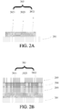
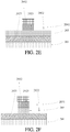
- FIGs. 2A to 2F illustrate schematic process diagrams of forming the conductive channel, the gate insulation layer, and the gate pattern on the substrate in the method for manufacturing the top-gated thin film transistors provided in the preferred embodiment of the present disclosure.
- step S101 forming the active layer 202 on the substrate 201.
- the active layer 202 includes a source region 2021, a drain region 2022, and a channel region 2023, wherein a material of the active layer 202 is indium gallium zinc oxide or amorphous silicon. More specifically, in this preferred embodiment, the active layer 202 is deposed on the substrate 201, then the source region 2021, the drain region 2022, and the channel region 2023 of the top-gated thin film transistors of the preferred embodiment are defined by a graphical process. It should be noted that the graphical process at least includes steps such as photoresist coating or dripping, exposure, development, photolithography, etc. These steps belong to the usual means in the art and will not be described here.
- step S102 as shown in FIG. 2B , forming a gate insulation layer 203, a gate metal layer 204, and a photoresist layer 205 on the active layer 202 in sequence.
- a material of the gate insulation layer 203 may include one or both of silicon oxide and silicon nitride. It should be noted that the step S102 merely disposes the gate insulation layer 203, the gate metal layer 204, and the photoresist layer 205 on the active layer 202, while the gate insulating layer 203, the gate metal layer 204, and the photoresist layer 205 may be formed by a deposition method well known to those skilled in the art and will not be described here.
- step S103 performing a patterning process for the photoresist layer 205 to form a first photoresist pattern 2051, wherein the first photoresist pattern 2051 includes a first shielding portion 20511 and two second shielding portions 20512 positioned at two sides of the first shielding portion 20511.
- a projection of the first shielding portion 20511 on the substrate 201 coincides with a projection of the channel region 2023 on the substrate 201.
- a thickness of the first shielding portion 20511 is larger than a thickness of the second shielding portion 20512.
- the patterning process for the photoresist layer 205 to form the first photoresist pattern 2051 includes: exposing the photoresist layer 205 by adopting a halftone mask; and developing the exposed photoresist layer 205 by a developing solution to form the first photoresist pattern 2051.
- step S104 etching the gate metal layer 204 by adopting the first photoresist pattern 2051 as a mask for forming a gate pattern 2041.
- the gate metal layer 204 may be etched by an etching method well known to those skilled in the art and will not be described here.
- the present disclosure emphasizes that the formed gate pattern 2041 coincides with the channel region 2023, i.e., the projection of the gate pattern 2041 on the substrate 201 coincides with the projection of the channel region 2023 on the substrate 201.
- step S105 performing an ashing process for the second shielding portion 20512 of the first photoresist pattern 2051 to remove the second shielding portion 20512 of the first photoresist pattern 2051 to form a second photoresist pattern 2052.
- the second shielding portion 20512 of the first photoresist pattern 2051 is formed by the step S103, so that the formed gate pattern 2041 does not suffer from an effect of metal over-etching and the phenomenon that the size does not coincide with the channel region 2023.
- the second shielding portion 20512 of the first photoresist pattern 2051 should be removed.
- the ashing process may be performed for the second shielding portion 20512 of the first photoresist pattern 2051 by adopting oxygen.
- step S106 etching the gate insulation layer 203 by adopting the second photoresist pattern 2052 as another mask for exposing the source region 2021 and the drain region 2022.
- step S107 as shown in FIG. 2F , performing a conductorizing process for the active layer to form a source contact region on the source region 2021 and to form a drain contact region on the drain region 2022, wherein the source contact region, the drain contact region, and the channel region 2023 commonly form a conducting channel.
- the conductorizing process for the active layer may be performed by adopting plasma.
- FIGs. 3A to 3C which illustrate schematic process diagrams of forming an inter-layers insulation layer, a source, and a drain in the method for manufacturing the top-gated thin film transistors provided in the preferred embodiment of the present disclosure.
- the method for manufacturing the top-gated thin film transistors provided from the preferred embodiment further includes a process of forming the inter-layers insulation layer, the source, and the drain, the process of forming the inter-layers insulation layer, the source, and the drain specifically includes the following.
- the inter-layers insulation layer 206 on the gate pattern 2041, the source contact region, and the drain contact region, and forming a first through hole 2061 and a second through hole 2062 passing through the inter-layers insulation layer 206, wherein the first through hole 2061 and the second through hole 2062 expose the source contact region and the drain contact region, respectively.
- stripping the second photoresist pattern may be achieved by soaking the second photoresist pattern in a peeling liquid.
- the method of manufacturing the top-gated thin film transistors of the preferred embodiment comprises forming a first photoresist pattern including the first shielding portion and a second shielding portion, and adopting the first photoresist pattern as the mask for etching the gate metal layer, so that the size of the gate pattern coincides with the size of the channel region of the conductive channel, to increase the control force of the gate to the conductive channel, thereby improving the performance of the device.
- the present disclosure further provides a top-gated thin film transistor which is produced by the above-described method of manufacturing the top-gated thin film transistors.
- the structure of the top-gated thin film transistor is characterized in that the size of the gate pattern coincides with the size of the channel region of the conductive channel.
- the top-gated thin film transistor may be referred to the same manufactured by the above-described preferred embodiment of the manufacturing the top-gated thin film transistors, and it will not be described here.
- the method of manufacturing top-gated thin film transistors according to the present disclosure includes forming the first photoresist pattern including the first shielding portion and the second shielding portion, and adopting the first photoresist pattern as the mask for etching the gate metal layer, so that the size of the gate pattern coincides with the size of the channel region of the conductive channel, to increase the control force of the gate to the conductive channel, thereby improving the performance of the device.
Landscapes
- Thin Film Transistor (AREA)
- Electrodes Of Semiconductors (AREA)
- Chemical & Material Sciences (AREA)
- Crystallography & Structural Chemistry (AREA)
Abstract
Description
- The present disclosure relates to a technical field of displays, and particularly to a method for manufacturing top-gated thin film transistors.
- Thin film transistors can be divided into bottom-gated thin film transistors and top-gated thin film transistors according to structure of the thin film transistors. In this way, parasitic capacitance, formed between a source/drain and a gate of the top-gated thin film transistor, may be significantly reduced, thereby increasing open-state current of the thin film transistor and enhancing operational speed of a device with the transistor, which facilitates reduced size of the device. Thus, it has become a hot industrial research area in recent years.
- In conventional methods for manufacturing top-gated thin film transistors, steps of forming a gate pattern specifically include forming a gate metal layer, and performing an etching process on the gate metal layer. However, in the process of etching the gate metal layer, the metal can easily be over-etched, such that a width of the gate pattern is smaller than a width of a channel region of a conductive channel, and the gate cannot completely control the conductive channel. Thus, current between the source and the drain is reduced, and performance of the device with thin film transistors is reduced.
- Therefore, it is necessary to provide a method for manufacturing top-gated thin film transistors to solve the problems which exist in the prior art.
- An object of the present disclosure is to provide a method for manufacturing top-gated thin film transistors, to enhance a control force for a conductive channel and a performance of device.
- The present disclosure provides a method for manufacturing top-gated thin film transistors. The method includes processes of forming a conductive channel, a gate insulation layer, and a gate pattern on a substrate;
wherein the processes of forming the conductive channel, the gate insulation layer, and the gate pattern on the substrate specifically include:
forming an active layer on the substrate, the active layer comprising a source region, a drain region, and a channel region;
forming a gate insulation layer, a gate metal layer, and a photoresist layer on the active layer in sequence;
performing a patterning process for the photoresist layer to form a first photoresist pattern, wherein the first photoresist pattern comprises a first shielding portion and two second shielding portions positioned at two sides of the first shielding portion; a projection of the first shielding portion on the substrate coincides with a projection of the channel region on the substrate; and a thickness of the first shielding portion is larger than a thickness of the second shielding portion;
etching the gate metal layer by adopting the first photoresist pattern as a mask for forming a gate pattern;
performing an ashing process for the second shielding portion of the first photoresist pattern to remove the second shielding portion of the first photoresist pattern to form a second photoresist pattern;
etching the gate insulation layer by adopting the second photoresist pattern as another mask for exposing the source region and the drain region; and
performing a conductorizing process for the active layer to form a source contact region on the source region and to form a drain contact region on the drain region, wherein the source contact region, the drain contact region, and the channel region commonly form a conducting channel;
wherein a projection of the gate pattern on the substrate coincides with a projection of the channel region on the substrate, and the ashing process is performed for the second shielding portion of the first photoresist pattern by adopting oxygen. - In the method for manufacturing the top-gated thin film transistors, the patterning process for the photoresist layer to form the first photoresist pattern includes:
exposing the photoresist layer by adopting a halftone mask, and developing the exposed photoresist layer by a developing solution to form the first photoresist pattern. - In the method for manufacturing the top-gated thin film transistors, a material of the active layer is indium gallium zinc oxide or amorphous silicon.
- In the method for manufacturing the top-gated thin film transistors, the manufacturing method further includes: a process of forming an inter-layers insulation layer, a source, and a drain,
wherein the process of forming the inter-layers insulation layer, the source, and the drain specifically comprises steps of: - stripping the second photoresist pattern;
- forming the inter-layers insulation layer on the gate pattern, the source contact region, and the drain contact region; and forming a first through hole and a second through hole passing through the inter-layers insulation layer, wherein the first through hole and the second through hole expose the source contact region and the drain contact region, respectively; and
- forming the source and the drain on the inter-layers insulation layer, wherein the source and the drain are contacted with the source contact region and the drain contact region through the first through hole and the second through hole, respectively.
- In the method for manufacturing the top-gated thin film transistors, the step of stripping the second photoresist pattern specifically includes: soaking the second photoresist pattern in a peeling liquid.
- In the method for manufacturing the top-gated thin film transistors, wherein a material of the gate insulation layer comprises one or both of silicon oxide and silicon nitride.
- In the method for manufacturing the top-gated thin film transistors, wherein the conductorizing process for the active layer is performed by adopting plasma.
- The present disclosure further provides a method for manufacturing top-gated thin film transistors, the method includes: a process of forming a conductive channel, a gate insulation layer, and a gate pattern on a substrate;
wherein the process of forming the conductive channel, the gate insulation layer, and the gate pattern on the substrate specifically includes: - forming an active layer on the substrate, the active layer including a source region, a drain region, and a channel region;
- forming a gate insulation layer, a gate metal layer, and a photoresist layer on the active layer in sequence;
- performing a patterning process for the photoresist layer to form a first photoresist pattern, wherein the first photoresist pattern comprises a first shielding portion and two second shielding portions positioned at two sides of the first shielding portion; a projection of the first shielding portion on the substrate coincides with a projection of the channel region on the substrate; and a thickness of the first shielding portion is larger than a thickness of the second shielding portion;
- etching the gate metal layer by adopting the first photoresist pattern as a mask for forming a gate pattern;
- performing an ashing process for the second shielding portion of the first photoresist pattern to remove the second shielding portion of the first photoresist pattern to form a second photoresist pattern;
- etching the gate insulation layer by adopting the second photoresist pattern as another mask for exposing the source region and the drain region; and
- performing a conductorizing process for the active layer to form a source contact region on the source region and to form a drain contact region on the drain region, wherein the source contact region, the drain contact region, and the channel region commonly form a conducting channel.
- In the method for manufacturing the top-gated thin film transistors according to the present disclosure, a projection of the gate pattern on the substrate coincides with a projection of the channel region on the substrate.
- In the method for manufacturing the top-gated thin film transistors according to the present disclosure, the patterning processing for the photoresist layer to form the first photoresist pattern includes:
exposing the photoresist layer by utilizing a halftone mask; and developing the exposed photoresist layer by a developing solution to form the first photoresist pattern. - In the method for manufacturing the top-gated thin film transistors according to the present disclosure, an ash processing is performed for the second shielding portion of the first photoresist pattern by adopting oxygen.
- In the method for manufacturing the top-gated thin film transistors according to the present disclosure, a material of the active layer is indium gallium zinc oxide or amorphous silicon.
- The method for manufacturing the top-gated thin film transistors according to the present disclosure further comprises: a process of forming an inter-layers insulation layer, a source, and a drain,
wherein the process of forming the inter-layers insulation layer, the source, and the drain specifically includes steps of: - stripping the second photoresist pattern;
- forming the inter-layers insulation layer on the gate pattern, the source contact region, and the drain contact region, and forming a first through hole and a second through hole passing through the inter-layers insulation layer, wherein the first through hole and the second through hole expose the source contact region and the drain contact region, respectively; and
- forming the source and the drain on the inter-layers insulation layer, wherein the source and the drain are contacted with the source contact region and the drain contact region through the first through hole and the second through hole, respectively.
- In the method for manufacturing the top-gated thin film transistors according to the present disclosure, the step of stripping the second photoresist pattern specifically includes: soaking the second photoresist pattern in a peeling liquid.
- In the method for manufacturing the top-gated thin film transistors according to the present disclosure, a material of the gate insulation layer comprises one or both of silicon oxide and silicon nitride.
- In the method for manufacturing the top-gated thin film transistors according to the present disclosure, the conductorizing process for the active layer is performed by adopting plasma.
- The method for manufacturing the top-gated thin film transistors according to the present disclosure includes forming the first photoresist pattern having the first shielding portion and the second shielding portion, and adopting the first photoresist pattern as the mask for etching the gate metal layer. Thus, the size of the gate pattern coincides with the size of the channel region of the conductive channel, the control force of the gate to the conductive channel is enhanced, and the performance of the device is improved.
- In order that the foregoing description of the present disclosure will become more clear, the preferred embodiments are given hereafter and are to be described in detail with reference to the accompanying drawings.
- The technical aspects and other advantageous effects of the present disclosure will be apparent from the following detailed description of specific embodiments of the disclosure taken in conjunction with the accompanying drawings.
-
FIG. 1 illustrates a flowchart of a method for manufacturing top-gated thin film transistors provided in a preferred embodiment of the present disclosure. -
FIGs. 2A to 2F illustrate schematic process diagrams of forming a conductive channel, a gate insulation layer, and a gate pattern on a substrate in the method for manufacturing the top-gated thin film transistors provided in the preferred embodiment of the present disclosure. -
FIGs. 3A to 3C illustrate schematic process diagrams of forming an inter-layers insulation layer, a source, and a drain in the method for manufacturing the top-gated thin film transistors provided in the preferred embodiment of the present disclosure. - The technical means and effects thereof will be further elucidated with reference to the preferred embodiments of the present disclosure and their accompanying drawings. Obviously, the described embodiments are merely a part of embodiments of the present disclosure, and not all embodiments. All other embodiments obtained by those of ordinary skill in the art without making creative work are within the scope of the present disclosure, based on embodiments of the present disclosure.
- A preferred embodiment of the present disclosure provides a method for manufacturing top-gated thin film transistors. The method includes forming a first photoresist pattern, etching a gate metal layer through adopting the first photoresist pattern as a mask, such that a projection of the gate pattern on a substrate and a projection of a gate insulation layer on the substrate both coincide with a projection of a channel region on the substrate. Thus, a control force of the gate to the conductive channel is enhanced.
- Referring to
FIG. 1 , which illustrates a flowchart of a method for manufacturing the top-gated thin film transistors provided in a preferred embodiment of the present disclosure. As shown inFIG. 1 , the preferred embodiment of the present disclosure provides the method for manufacturing the top-gated thin film transistors. The method is intended to increase the control force of the gate to the conductive channel, and is specifically achieved by the size of the gate pattern formed by precision control coinciding with the size of the channel region of the conductive channel. - The method for manufacturing the top-gated thin film transistors will be described in detail below with reference to specific embodiments. The method includes processes of forming a conductive channel, a gate insulation layer, and a gate pattern on a substrate. In addition, the processes of forming the conductive channel, the gate insulation layer, and the gate pattern on the substrate specifically include the following steps.
- In step S101, forming an active layer on the substrate, the active layer including a source region, a drain region, and a channel region.
- In step S102, forming a gate insulation layer, a gate metal layer, and a photoresist layer on the active layer in sequence.
- In step S103, performing a patterning process for the photoresist layer to form a first photoresist pattern, wherein the first photoresist pattern includes a first shielding portion and two second shielding portions positioned at two sides of the first shielding portion; a projection of the first shielding portion on the substrate coincides with a projection of the channel region on the substrate; and a thickness of the first shielding portion is larger than a thickness of the second shielding portion.
- In step S104, etching the gate metal layer by adopting the first photoresist pattern as a mask for forming a gate pattern.
- In step S105, performing an ashing process for the second shielding portion of the first photoresist pattern to remove the second shielding portion of the first photoresist pattern to form a second photoresist pattern.
- In step S106, etching the gate insulation layer by adopting the second photoresist pattern as a mask for exposing the source region and the drain region.
- In step S107, performing a conductorizing process for the active layer to form a source contact region on the source region and to form a drain contact region on the drain region, wherein the source contact region, the drain contact region, and the channel region commonly form a conducting channel.
- It should be noted that, in the method for manufacturing top-gated thin film transistors of the present disclosure, in order to suppress that the size of the gate does not coincide with the size of the channel region of the conductive channel due to the metal from being over-etched when the gate pattern is formed. The method is achieved by forming the first photoresist pattern, and adopting the first photoresist pattern as the mask for etching the gate metal layer to form a gate with a size coinciding with a size of the channel region of the conductive channel, thereby increasing the control force of the gate to the conductive channel and improving the performance of the device having the transistor.
- Processes of the method for manufacturing the top-gated thin film transistors will be described in detail below with reference to
FIGs. 2A to 2F , which illustrate schematic process diagrams of forming the conductive channel, the gate insulation layer, and the gate pattern on the substrate in the method for manufacturing the top-gated thin film transistors provided in the preferred embodiment of the present disclosure. - In step S101, as shown in
FIG. 2A , forming theactive layer 202 on thesubstrate 201. Theactive layer 202 includes asource region 2021, adrain region 2022, and achannel region 2023, wherein a material of theactive layer 202 is indium gallium zinc oxide or amorphous silicon. More specifically, in this preferred embodiment, theactive layer 202 is deposed on thesubstrate 201, then thesource region 2021, thedrain region 2022, and thechannel region 2023 of the top-gated thin film transistors of the preferred embodiment are defined by a graphical process. It should be noted that the graphical process at least includes steps such as photoresist coating or dripping, exposure, development, photolithography, etc. These steps belong to the usual means in the art and will not be described here. - In step S102, as shown in
FIG. 2B , forming agate insulation layer 203, agate metal layer 204, and aphotoresist layer 205 on theactive layer 202 in sequence. Preferably, a material of thegate insulation layer 203 may include one or both of silicon oxide and silicon nitride. It should be noted that the step S102 merely disposes thegate insulation layer 203, thegate metal layer 204, and thephotoresist layer 205 on theactive layer 202, while thegate insulating layer 203, thegate metal layer 204, and thephotoresist layer 205 may be formed by a deposition method well known to those skilled in the art and will not be described here. - In step S103, as shown in conjunction with
FIGs. 2B and2C , performing a patterning process for thephotoresist layer 205 to form afirst photoresist pattern 2051, wherein thefirst photoresist pattern 2051 includes afirst shielding portion 20511 and twosecond shielding portions 20512 positioned at two sides of thefirst shielding portion 20511. In addition, a projection of thefirst shielding portion 20511 on thesubstrate 201 coincides with a projection of thechannel region 2023 on thesubstrate 201. Furthermore, a thickness of thefirst shielding portion 20511 is larger than a thickness of thesecond shielding portion 20512. - More specifically, in the step S103, the patterning process for the
photoresist layer 205 to form thefirst photoresist pattern 2051 includes: exposing thephotoresist layer 205 by adopting a halftone mask; and developing the exposedphotoresist layer 205 by a developing solution to form thefirst photoresist pattern 2051. - In step S104, as shown in conjunction with
FIGs. 2C and 2D , etching thegate metal layer 204 by adopting thefirst photoresist pattern 2051 as a mask for forming agate pattern 2041. It should be noted that thegate metal layer 204 may be etched by an etching method well known to those skilled in the art and will not be described here. The present disclosure emphasizes that the formedgate pattern 2041 coincides with thechannel region 2023, i.e., the projection of thegate pattern 2041 on thesubstrate 201 coincides with the projection of thechannel region 2023 on thesubstrate 201. - In step S105, as shown in
FIG. 2E , performing an ashing process for thesecond shielding portion 20512 of thefirst photoresist pattern 2051 to remove thesecond shielding portion 20512 of thefirst photoresist pattern 2051 to form asecond photoresist pattern 2052. Specifically, thesecond shielding portion 20512 of thefirst photoresist pattern 2051 is formed by the step S103, so that the formedgate pattern 2041 does not suffer from an effect of metal over-etching and the phenomenon that the size does not coincide with thechannel region 2023. However, in step S105, in order to match the size of thegate insulating layer 203 to the size of thegate pattern 2041, thesecond shielding portion 20512 of thefirst photoresist pattern 2051 should be removed. - Preferably, the ashing process may be performed for the
second shielding portion 20512 of thefirst photoresist pattern 2051 by adopting oxygen. - In step S106, as shown in conjunction with
FIGs. 2E and 2F , etching thegate insulation layer 203 by adopting thesecond photoresist pattern 2052 as another mask for exposing thesource region 2021 and thedrain region 2022. - In step S107, as shown in
FIG. 2F , performing a conductorizing process for the active layer to form a source contact region on thesource region 2021 and to form a drain contact region on thedrain region 2022, wherein the source contact region, the drain contact region, and thechannel region 2023 commonly form a conducting channel. Preferably, the conductorizing process for the active layer may be performed by adopting plasma. - In addition, referring to
FIGs. 3A to 3C , which illustrate schematic process diagrams of forming an inter-layers insulation layer, a source, and a drain in the method for manufacturing the top-gated thin film transistors provided in the preferred embodiment of the present disclosure. The method for manufacturing the top-gated thin film transistors provided from the preferred embodiment further includes a process of forming the inter-layers insulation layer, the source, and the drain, the process of forming the inter-layers insulation layer, the source, and the drain specifically includes the following. - Firstly, as shown in conjunction with
FIGs. 2F and3A , stripping thesecond photoresist pattern 2052. - Then, as shown in
FIG. 3B , forming theinter-layers insulation layer 206 on thegate pattern 2041, the source contact region, and the drain contact region, and forming a first throughhole 2061 and a second throughhole 2062 passing through theinter-layers insulation layer 206, wherein the first throughhole 2061 and the second throughhole 2062 expose the source contact region and the drain contact region, respectively. - Finally, as shown in conjunction with
FIGs. 3B and3C , forming thesource 2071 and thedrain 2072 on theinter-layers insulation layer 206, wherein thesource 2071 and thedrain 2072 are contacted with the source contact region and the drain contact region through the first throughhole 2061 and the second throughhole 2062, respectively. - Preferably, stripping the second photoresist pattern may be achieved by soaking the second photoresist pattern in a peeling liquid.
- The method of manufacturing the top-gated thin film transistors of the preferred embodiment comprises forming a first photoresist pattern including the first shielding portion and a second shielding portion, and adopting the first photoresist pattern as the mask for etching the gate metal layer, so that the size of the gate pattern coincides with the size of the channel region of the conductive channel, to increase the control force of the gate to the conductive channel, thereby improving the performance of the device.
- The present disclosure further provides a top-gated thin film transistor which is produced by the above-described method of manufacturing the top-gated thin film transistors. The structure of the top-gated thin film transistor is characterized in that the size of the gate pattern coincides with the size of the channel region of the conductive channel. Specifically, the top-gated thin film transistor may be referred to the same manufactured by the above-described preferred embodiment of the manufacturing the top-gated thin film transistors, and it will not be described here.
- The method of manufacturing top-gated thin film transistors according to the present disclosure includes forming the first photoresist pattern including the first shielding portion and the second shielding portion, and adopting the first photoresist pattern as the mask for etching the gate metal layer, so that the size of the gate pattern coincides with the size of the channel region of the conductive channel, to increase the control force of the gate to the conductive channel, thereby improving the performance of the device.
- While the present disclosure has been disclosed with reference to preferred embodiments as disclosed above, the above-described embodiments are not intended to limit the present disclosure, and a person having ordinary skill in the art will be able to make various changes and modifications without departing from the spirit and scope of the present disclosure, and thus the scope of the present disclosure is defined by the scope of the claims.
Claims (17)
- A method for manufacturing top-gated thin film transistors, comprising:forming a conductive channel, a gate insulation layer, and a gate pattern on a substrate;
wherein the forming the conductive channel, the gate insulation layer, and the gate pattern on the substrate specifically comprise:forming an active layer on the substrate, the active layer comprising a source region, a drain region, and a channel region;forming a gate insulation layer, a gate metal layer, and a photoresist layer on the active layer in sequence;performing a patterning process for the photoresist layer to form a first photoresist pattern, wherein the first photoresist pattern comprises a first shielding portion and two second shielding portions positioned at two sides of the first shielding portion; a projection of the first shielding portion on the substrate coincides with a projection of the channel region on the substrate; and a thickness of the first shielding portion is larger than a thickness of the second shielding portion;etching the gate metal layer by adopting the first photoresist pattern as a mask for forming a gate pattern;performing an ashing process for the second shielding portion of the first photoresist pattern to remove the second shielding portion of the first photoresist pattern to form a second photoresist pattern;etching the gate insulation layer by adopting the second photoresist pattern as another mask for exposing the source region and the drain region; andperforming a conductorizing process for the active layer to form a source contact region on the source region and to form a drain contact region on the drain region, wherein the source contact region, the drain contact region, and the channel region commonly forma conducting channel;wherein a projection of the gate pattern on the substrate coincides with a projection of the channel region on the substrate, and the ashing process is performed for the second shielding portion of the first photoresist pattern by adopting oxygen. - The method for manufacturing the top-gated thin film transistors as claimed in claim 1, wherein the patterning process for the photoresist layer to form the first photoresist pattern comprises exposing the photoresist layer by adopting a halftone mask, and developing the exposed photoresist layer by a developing solution to form the first photoresist pattern.
- The method for manufacturing the top-gated thin film transistors as claimed in claim 1, wherein a material of the active layer is indium gallium zinc oxide or amorphous silicon.
- The method for manufacturing the top-gated thin film transistors as claimed in claim 1, further comprising: forming an inter-layers insulation layer, a source, and a drain, wherein the processes of forming the inter-layers insulation layer, the source, and the drain specifically comprises steps of:stripping the second photoresist pattern;forming the inter-layers insulation layer on the gate pattern, the source contact region, and the drain contact region; and forming a first through hole and a second through hole passing through the inter-layers insulation layer, wherein the first through hole and the second through hole expose the source contact region and the drain contact region, respectively; andforming the source and the drain on the inter-layers insulation layer, wherein the source and the drain are contacted with the source contact region and the drain contact region through the first through hole and the second through hole, respectively.
- The method for manufacturing the top-gated thin film transistors as claimed in claim 4, wherein the step of stripping the second photoresist pattern specifically comprises: soaking the second photoresist pattern in a peeling liquid.
- The method for manufacturing the top-gated thin film transistors as claimed in claim 1, wherein a material of the gate insulation layer comprises one or both of silicon oxide and silicon nitride.
- The method for manufacturing the top-gated thin film transistors as claimed in claim 1, wherein the conductorizing process for the active layer is performed by adopting plasma.
- A method for manufacturing top-gated thin film transistors, comprising:forming a conductive channel, a gate insulation layer, and a gate pattern on a substrate;
wherein the forming the conductive channel, the gate insulation layer, and the gate pattern on the substrate specifically comprises:forming an active layer on the substrate, the active layer comprising a source region, a drain region, and a channel region;forming a gate insulation layer, a gate metal layer, and a photoresist layer on the active layer in sequence;performing a patterning process for the photoresist layer to form a first photoresist pattern, wherein the first photoresist pattern comprises a first shielding portion and two second shielding portions positioned at two sides of the first shielding portion; a projection of the first shielding portion on the substrate coincides with a projection of the channel region on the substrate; and a thickness of the first shielding portion is larger than a thickness of the second shielding portion;etching the gate metal layer by adopting the first photoresist pattern as a mask for forming a gate pattern;performing an ashing process for the second shielding portion of the first photoresist pattern to remove the second shielding portion of the first photoresist pattern to form a second photoresist pattern;etching the gate insulation layer by adopting the second photoresist pattern as another mask for exposing the source region and the drain region; andperforming a conductorizing process for the active layer to form a source contact region on the source region and to form a drain contact region on the drain region, wherein the source contact region, the drain contact region, and the channel region commonly form a conducting channel. - The method for manufacturing the top-gated thin film transistors as claimed in claim 8, wherein a projection of the gate pattern on the substrate coincides with a projection of the channel region on the substrate.
- The method for manufacturing the top-gated thin film transistors as claimed in claim 8, wherein the patterning processing for the photoresist layer to form the first photoresist pattern comprises exposing the photoresist layer by utilizing a halftone mask, and developing the exposed photoresist layer by a developing solution to form the first photoresist pattern.
- The method for manufacturing the top-gated thin film transistors as claimed in claim 9, wherein the patterning processing for the photoresist layer to form the first photoresist pattern comprises exposing the photoresist layer by utilizing a halftone mask, and developing the exposed photoresist layer by a developing solution to form the first photoresist pattern.
- The method for manufacturing the top-gated thin film transistors as claimed in claim 8, wherein an ash processing is performed for the second shielding portion of the first photoresist pattern by adopting oxygen.
- The method for manufacturing the top-gated thin film transistors as claimed in claim 8, wherein a material of the active layer is indium gallium zinc oxide or amorphous silicon.
- The method for manufacturing the top-gated thin film transistors as claimed in claim 8, further comprising: a process of forming an inter-layers insulation layer, a source, and a drain, wherein the processes of forming the inter-layers insulation layer, the source, and the drain specifically comprises steps of:stripping the second photoresist pattern;forming the inter-layers insulation layer on the gate pattern, the source contact region, and the drain contact region, and forming a first through hole and a second through hole passing through the inter-layers insulation layer, wherein the first through hole and the second through hole expose the source contact region and the drain contact region, respectively; andforming the source and the drain on the inter-layers insulation layer, wherein the source and the drain are contacted with the source contact region and the drain contact region through the first through hole and the second through hole, respectively.
- The method for manufacturing the top-gated thin film transistors as claimed in claim 14, wherein the step of stripping the second photoresist pattern specifically comprises: soaking the second photoresist pattern in a peeling liquid.
- The method for manufacturing the top-gated thin film transistors as claimed in claim 8, wherein a material of the gate insulation layer comprises one or both of silicon oxide and silicon nitride.
- The method for manufacturing the top-gated thin film transistors as claimed in claim 8, wherein the conductorizing process for the active layer is performed by adopting plasma.
Applications Claiming Priority (2)
| Application Number | Priority Date | Filing Date | Title |
|---|---|---|---|
| CN201710592932.3A CN107464836B (en) | 2017-07-19 | 2017-07-19 | Manufacturing method of top gate type thin film transistor and top gate type thin film transistor |
| PCT/CN2017/101162 WO2019015054A1 (en) | 2017-07-19 | 2017-09-11 | Fabrication method for top-gate thin film transistor |
Publications (2)
| Publication Number | Publication Date |
|---|---|
| EP3657547A1 true EP3657547A1 (en) | 2020-05-27 |
| EP3657547A4 EP3657547A4 (en) | 2021-04-07 |
Family
ID=60546833
Family Applications (1)
| Application Number | Title | Priority Date | Filing Date |
|---|---|---|---|
| EP17918145.8A Withdrawn EP3657547A4 (en) | 2017-07-19 | 2017-09-11 | TOP GRID THIN FILM TRANSISTOR MANUFACTURING PROCESS |
Country Status (6)
| Country | Link |
|---|---|
| US (1) | US10204942B1 (en) |
| EP (1) | EP3657547A4 (en) |
| JP (1) | JP2020526043A (en) |
| KR (1) | KR102228288B1 (en) |
| CN (1) | CN107464836B (en) |
| WO (1) | WO2019015054A1 (en) |
Families Citing this family (2)
| Publication number | Priority date | Publication date | Assignee | Title |
|---|---|---|---|---|
| KR20230038357A (en) | 2021-09-10 | 2023-03-20 | 삼성전자주식회사 | semiconductor device and fabricating the same |
| KR102693356B1 (en) | 2022-07-21 | 2024-08-07 | 포항공과대학교 산학협력단 | Micro-patterning organic thin film transistor and manufacturing method thereof |
Family Cites Families (22)
| Publication number | Priority date | Publication date | Assignee | Title |
|---|---|---|---|---|
| KR100248119B1 (en) * | 1997-05-01 | 2000-03-15 | 구자홍 | Thin-film transistor and method for manufacturing thereof |
| KR100333978B1 (en) * | 1998-12-28 | 2003-06-02 | 삼성전자 주식회사 | Manufacturing method of thin film transistor substrate for liquid crystal display device |
| KR100412121B1 (en) * | 2001-03-31 | 2003-12-31 | 비오이 하이디스 테크놀로지 주식회사 | METHOD FOR MANUFACTURING OF Thin Film Transistor |
| US6963083B2 (en) * | 2003-06-30 | 2005-11-08 | Lg.Philips Lcd Co., Ltd. | Liquid crystal display device having polycrystalline TFT and fabricating method thereof |
| KR100648221B1 (en) * | 2004-07-09 | 2006-11-24 | 비오이 하이디스 테크놀로지 주식회사 | Array substrate manufacturing method of thin film transistor liquid crystal display |
| US7033902B2 (en) * | 2004-09-23 | 2006-04-25 | Toppoly Optoelectronics Corp. | Method for making thin film transistors with lightly doped regions |
| KR101143005B1 (en) * | 2004-12-14 | 2012-05-08 | 삼성전자주식회사 | Mask and method for manufacturing semiconductor device and thin film transistor array panel using the mask |
| KR101239889B1 (en) * | 2005-08-13 | 2013-03-06 | 삼성디스플레이 주식회사 | Thin film transistor plate and method of fabricating the same |
| KR101206038B1 (en) * | 2006-12-18 | 2012-11-28 | 삼성전자주식회사 | Method of manufacturing thin film transistor having lightly doped drain region |
| KR101108175B1 (en) * | 2010-06-09 | 2012-01-31 | 삼성모바일디스플레이주식회사 | Thin film transistor, array substrate for display device comprising same, and manufacturing method thereof |
| US9105652B2 (en) * | 2011-05-24 | 2015-08-11 | Sharp Kabushiki Kaisha | Method of manufacturing semiconductor device |
| CN102637632B (en) * | 2011-06-10 | 2014-12-10 | 京东方科技集团股份有限公司 | Thin-film transistor array and method for manufacturing same |
| CN102651341B (en) * | 2012-01-13 | 2014-06-11 | 京东方科技集团股份有限公司 | Manufacturing method of TFT (Thin Film Transistor) array substrate |
| KR20130111872A (en) * | 2012-04-02 | 2013-10-11 | 삼성디스플레이 주식회사 | Thin film transistor, thin film transistor array panel including the same and manufacturing method thereof |
| CN102723269B (en) * | 2012-06-21 | 2015-04-01 | 京东方科技集团股份有限公司 | Array base plate, method for manufacturing same, and display device |
| KR102039424B1 (en) * | 2012-06-22 | 2019-11-01 | 엘지디스플레이 주식회사 | Method of fabricating oxide thin film transistor |
| KR101454190B1 (en) * | 2012-12-07 | 2014-11-03 | 엘지디스플레이 주식회사 | Array substrate and method of fabricating the same |
| KR102101863B1 (en) * | 2013-01-07 | 2020-04-21 | 삼성디스플레이 주식회사 | Thin film transistor, method for fabricting the same and display apparatus having the same |
| CN103227148B (en) * | 2013-04-02 | 2015-12-23 | 京东方科技集团股份有限公司 | A kind of array base palte preparation method and array base palte and display unit |
| CN104465405B (en) * | 2014-12-30 | 2017-09-22 | 京东方科技集团股份有限公司 | The preparation method of thin film transistor (TFT) and the preparation method of array base palte |
| KR102458907B1 (en) * | 2015-12-29 | 2022-10-25 | 엘지디스플레이 주식회사 | Organic light emitting display and method of fabricating the same |
| CN105762195B (en) * | 2016-03-04 | 2019-07-26 | 武汉华星光电技术有限公司 | Metal oxide thin-film transistor and preparation method thereof |
-
2017
- 2017-07-19 CN CN201710592932.3A patent/CN107464836B/en active Active
- 2017-09-11 EP EP17918145.8A patent/EP3657547A4/en not_active Withdrawn
- 2017-09-11 WO PCT/CN2017/101162 patent/WO2019015054A1/en not_active Ceased
- 2017-09-11 US US15/742,153 patent/US10204942B1/en active Active
- 2017-09-11 JP JP2020500627A patent/JP2020526043A/en active Pending
- 2017-09-11 KR KR1020207004739A patent/KR102228288B1/en active Active
Also Published As
| Publication number | Publication date |
|---|---|
| US20190027515A1 (en) | 2019-01-24 |
| KR20200024327A (en) | 2020-03-06 |
| WO2019015054A1 (en) | 2019-01-24 |
| KR102228288B1 (en) | 2021-03-17 |
| JP2020526043A (en) | 2020-08-27 |
| CN107464836A (en) | 2017-12-12 |
| EP3657547A4 (en) | 2021-04-07 |
| US10204942B1 (en) | 2019-02-12 |
| CN107464836B (en) | 2020-04-10 |
Similar Documents
| Publication | Publication Date | Title |
|---|---|---|
| US9099440B2 (en) | Manufacturing method of array substrate, array substrate and display | |
| CN108122932B (en) | Array substrate and preparation method thereof | |
| CN109509707B (en) | Display panel, array substrate, thin film transistor and manufacturing method thereof | |
| US20200035709A1 (en) | Method for manufacturing thin-film transistor array substrate and thin-film transistor array substrate | |
| CN103715096A (en) | Thin film thyristor and manufacturing method thereof and array substrate and manufacturing method thereof | |
| CN105990449A (en) | Thin film transistor and manufacturing method thereof | |
| JP2017520914A (en) | THIN FILM TRANSISTOR AND METHOD FOR MANUFACTURING SAME, ARRAY SUBSTRATE, AND DISPLAY DEVICE | |
| CN104465405A (en) | Manufacturing method of thin film transistor and manufacturing method of array substrate | |
| CN110190031A (en) | A kind of preparation method of thin film transistor base plate | |
| WO2017008347A1 (en) | Array substrate, manufacturing method for array substrate, and display device | |
| WO2020232747A1 (en) | Thin-film transistor device and preparation method therefor | |
| CN106876281A (en) | A kind of thin film transistor (TFT) and preparation method thereof, array base palte | |
| CN108878515B (en) | Thin film transistor, preparation method thereof and array substrate | |
| CN105374827A (en) | Display device and method for manufacturing the same | |
| WO2016029551A1 (en) | Method for manufacturing thin film transistor and thin film transistor | |
| WO2020252955A1 (en) | Array substrate preparation method and array substrate preparation system | |
| CN104392928A (en) | Manufacturing method of film transistor | |
| CN107735853A (en) | Method for fabricating thin film transistor and array base palte | |
| US10204942B1 (en) | Method for manufacturing top-gated thin film transistors | |
| CN105990332A (en) | Thin film transistor substrate and display panel thereof | |
| EP3128558B1 (en) | Thin film transistor and manufacturing method therefor and display device | |
| US20190252414A1 (en) | Method for manufacturing thin film transistor | |
| CN103779232B (en) | A kind of manufacture method of thin film transistor (TFT) | |
| CN110112072A (en) | The manufacturing method and array substrate of array substrate | |
| US11889721B2 (en) | Display substrate, manufacturing method thereof and display device |
Legal Events
| Date | Code | Title | Description |
|---|---|---|---|
| STAA | Information on the status of an ep patent application or granted ep patent |
Free format text: STATUS: THE INTERNATIONAL PUBLICATION HAS BEEN MADE |
|
| PUAI | Public reference made under article 153(3) epc to a published international application that has entered the european phase |
Free format text: ORIGINAL CODE: 0009012 |
|
| STAA | Information on the status of an ep patent application or granted ep patent |
Free format text: STATUS: REQUEST FOR EXAMINATION WAS MADE |
|
| 17P | Request for examination filed |
Effective date: 20200214 |
|
| AK | Designated contracting states |
Kind code of ref document: A1 Designated state(s): AL AT BE BG CH CY CZ DE DK EE ES FI FR GB GR HR HU IE IS IT LI LT LU LV MC MK MT NL NO PL PT RO RS SE SI SK SM TR |
|
| AX | Request for extension of the european patent |
Extension state: BA ME |
|
| DAV | Request for validation of the european patent (deleted) | ||
| DAX | Request for extension of the european patent (deleted) | ||
| A4 | Supplementary search report drawn up and despatched |
Effective date: 20210309 |
|
| RIC1 | Information provided on ipc code assigned before grant |
Ipc: H01L 29/786 20060101ALI20210302BHEP Ipc: H01L 29/06 20060101ALI20210302BHEP Ipc: H01L 21/336 20060101AFI20210302BHEP |
|
| STAA | Information on the status of an ep patent application or granted ep patent |
Free format text: STATUS: THE APPLICATION IS DEEMED TO BE WITHDRAWN |
|
| 18D | Application deemed to be withdrawn |
Effective date: 20211006 |