EP3657179A2 - Single input circuit for receiving output from a di/dt sensor or current transformer and circuit breaker including same - Google Patents
Single input circuit for receiving output from a di/dt sensor or current transformer and circuit breaker including same Download PDFInfo
- Publication number
- EP3657179A2 EP3657179A2 EP19209007.4A EP19209007A EP3657179A2 EP 3657179 A2 EP3657179 A2 EP 3657179A2 EP 19209007 A EP19209007 A EP 19209007A EP 3657179 A2 EP3657179 A2 EP 3657179A2
- Authority
- EP
- European Patent Office
- Prior art keywords
- input
- circuit
- output
- sensor
- current
- Prior art date
- Legal status (The legal status is an assumption and is not a legal conclusion. Google has not performed a legal analysis and makes no representation as to the accuracy of the status listed.)
- Granted
Links
Images

Classifications
-
- G—PHYSICS
- G05—CONTROLLING; REGULATING
- G05B—CONTROL OR REGULATING SYSTEMS IN GENERAL; FUNCTIONAL ELEMENTS OF SUCH SYSTEMS; MONITORING OR TESTING ARRANGEMENTS FOR SUCH SYSTEMS OR ELEMENTS
- G05B19/00—Program-control systems
- G05B19/02—Program-control systems electric
- G05B19/04—Program control other than numerical control, i.e. in sequence controllers or logic controllers
- G05B19/042—Program control other than numerical control, i.e. in sequence controllers or logic controllers using digital processors
- G05B19/0423—Input/output
-
- G—PHYSICS
- G01—MEASURING; TESTING
- G01R—MEASURING ELECTRIC VARIABLES; MEASURING MAGNETIC VARIABLES
- G01R15/00—Details of measuring arrangements of the types provided for in groups G01R17/00 - G01R29/00, G01R33/00 - G01R33/26 or G01R35/00
- G01R15/14—Adaptations providing voltage or current isolation, e.g. for high-voltage or high-current networks
- G01R15/18—Adaptations providing voltage or current isolation, e.g. for high-voltage or high-current networks using inductive devices, e.g. transformers
- G01R15/181—Adaptations providing voltage or current isolation, e.g. for high-voltage or high-current networks using inductive devices, e.g. transformers using coils without a magnetic core, e.g. Rogowski coils
-
- H—ELECTRICITY
- H01—ELECTRIC ELEMENTS
- H01F—MAGNETS; INDUCTANCES; TRANSFORMERS; SELECTION OF MATERIALS FOR THEIR MAGNETIC PROPERTIES
- H01F27/00—Details of transformers or inductances, in general
- H01F27/42—Circuits specially adapted for the purpose of modifying, or compensating for, electric characteristics of transformers, reactors, or choke coils
- H01F27/422—Circuits specially adapted for the purpose of modifying, or compensating for, electric characteristics of transformers, reactors, or choke coils for instrument transformers
- H01F27/427—Circuits specially adapted for the purpose of modifying, or compensating for, electric characteristics of transformers, reactors, or choke coils for instrument transformers for current transformers
-
- G—PHYSICS
- G01—MEASURING; TESTING
- G01R—MEASURING ELECTRIC VARIABLES; MEASURING MAGNETIC VARIABLES
- G01R15/00—Details of measuring arrangements of the types provided for in groups G01R17/00 - G01R29/00, G01R33/00 - G01R33/26 or G01R35/00
- G01R15/14—Adaptations providing voltage or current isolation, e.g. for high-voltage or high-current networks
- G01R15/18—Adaptations providing voltage or current isolation, e.g. for high-voltage or high-current networks using inductive devices, e.g. transformers
- G01R15/183—Adaptations providing voltage or current isolation, e.g. for high-voltage or high-current networks using inductive devices, e.g. transformers using transformers with a magnetic core
-
- G—PHYSICS
- G01—MEASURING; TESTING
- G01R—MEASURING ELECTRIC VARIABLES; MEASURING MAGNETIC VARIABLES
- G01R19/00—Arrangements for measuring currents or voltages or for indicating presence or sign thereof
- G01R19/0023—Measuring currents or voltages from sources with high internal resistance by means of measuring circuits with high input impedance, e.g. OP-amplifiers
-
- G—PHYSICS
- G01—MEASURING; TESTING
- G01R—MEASURING ELECTRIC VARIABLES; MEASURING MAGNETIC VARIABLES
- G01R19/00—Arrangements for measuring currents or voltages or for indicating presence or sign thereof
- G01R19/0092—Measuring current only
-
- G—PHYSICS
- G05—CONTROLLING; REGULATING
- G05B—CONTROL OR REGULATING SYSTEMS IN GENERAL; FUNCTIONAL ELEMENTS OF SUCH SYSTEMS; MONITORING OR TESTING ARRANGEMENTS FOR SUCH SYSTEMS OR ELEMENTS
- G05B2219/00—Program-control systems
- G05B2219/20—Pc systems
- G05B2219/24—Pc safety
- G05B2219/24215—Scada supervisory control and data acquisition
-
- H—ELECTRICITY
- H02—GENERATION; CONVERSION OR DISTRIBUTION OF ELECTRIC POWER
- H02H—EMERGENCY PROTECTIVE CIRCUIT ARRANGEMENTS
- H02H3/00—Emergency protective circuit arrangements for automatic disconnection directly responsive to an undesired change from normal electric working condition with or without subsequent reconnection ; integrated protection
- H02H3/08—Emergency protective circuit arrangements for automatic disconnection directly responsive to an undesired change from normal electric working condition with or without subsequent reconnection ; integrated protection responsive to excess current
Definitions
- the disclosed concept relates generally to arrangements for sensing current, and, more particularly, to arrangements for sensing current used in conjunction with circuit breakers.
- the disclosed concept also relates to circuit breakers including such arrangements.
- a current sensor mounted external the breaker.
- Such a sensor may be used to sense an external neutral current, a ground current, or wrapped around multiple conductors to sense a current imbalance.
- the application was filled by current transformers.
- Rogowski coils have become more popular for several reasons: they can be made smaller and lighter than current transformers; they can be more easily made in split core configurations providing for a simpler installation; and they do not suffer from the effects of saturation.
- di/dt sensors e.g., without limitation, Rogowski coils
- the voltages are typically small, around 100 ⁇ V/A, with their function being maintained only for relatively high impedance loads.
- a circuit is adapted to receive input from either a current transformer or a di/dt sensor and to output a signal corresponding to the input.
- a circuit comprises: an input pair having a first input and a second input; a first output; a second output; a current transformer input circuit connected between the first input and the second input; and a di/dt sensor input circuit connected between the first input and the second input, wherein the current transformer input circuit is configured to receive output from a current transformer connected to the input pair and to output a signal representative of the current sensed thereby via the first output, and wherein the di/dt sensor input circuit is configured to receive output from a di/dt sensor connected to the input pair and to output a signal representative of the current or time rate of change of the current sensed thereby via the second output.
- the current transformer input circuit and the di/dt sensor input circuit may be connected in a parallel arrangement.
- the circuit may further comprise: a third circuit connected between the first input and the second input, the third circuit comprising: a ground connected between the first input and the second input, a fifth resistor connected in parallel with a second capacitor connected between the first input and the ground, and a sixth resistor connected in parallel with a third capacitor connected between the ground and the second input.
- the current transformer input circuit, the di/dt sensor input circuit, and the third circuit may be connected in a parallel arrangement between the first input and the second input.
- the circuit may further comprise: a third circuit connected between the first input and the second input, the third circuit comprising: a first arrangement comprising: a ground connected between the first input and the second input; a fifth resistor connected between the first input and the ground; and a sixth resistor connected between the ground and the second input; and a second arrangement comprising a third zener diode and a fourth zener diode connected opposing in series between the first input and the second input.
- the current transformer input circuit may comprise: a sense resistor connected between the first input and the second input; a first resistor connected in parallel with one of either a first transient voltage suppression diode or a first Zener diode connected between the first input and the sense resistor; a second resistor connected in parallel with another one of a second transient voltage suppression diode or a second Zener diode connected between the sense resistor and the second input; and a first amplifier having a first input connected on a first side of the sense resistor, a second input connected on an opposite second side of the sense resistor, and an output connected to the first output.
- the current transformer input circuit may comprise: a sense resistor connected between the first input and the second input; a first field effect transistor connected between the first input and the sense resistor; a second field effect transistor connected between the sense resistor and the second input; and a first amplifier having a first input connected on a first side of the sense resistor, a second input connected on an opposite second side of the sense resistor, and an output connected to the first output.
- the di/dt sensor input circuit may comprise: a first capacitor connected between the first input and the second input; a third resistor connected between the first input and the first capacitor; a fourth resistor connected between the first capacitor and the second input; and a second amplifier having a first input connected on a first side of the first capacitor and a second input connected on an opposite second side of the first capacitor, and an output connected to the second output.
- the di/dt sensor input circuit may comprise: a first capacitor connected between the first input and the second input; a third resistor connected between the first input and the first capacitor; a fourth resistor connected between the first capacitor and the second input; and a second amplifier having a first input connected on a first side of the first capacitor and a second input connected on an opposite second side of the first capacitor, and an output connected to the second output.
- the di/dt sensor input circuit may comprise: a second amplifier having a first input, a second input, and an output connected to the second output; a third resistor connected between the first input of the circuit and the first input of the second amplifier; and a fourth resistor connected between the second input of the circuit and the second input of the second amplifier.
- the di/dt sensor input circuit may comprise: a second amplifier having a first input, a second input, and an output connected to the second output; a third resistor connected between the first input of the circuit and the first input of the second amplifier; and a fourth resistor connected between the second input of the circuit and the second input of the second amplifier.
- the di/dt sensor input circuit may comprise: a second amplifier having a first input, a second input, and an output connected to the second output; a third resistor connected between the first input of the circuit and the first input of the second amplifier; and a fourth resistor connected between the second input of the circuit and the second input of the second amplifier.
- a circuit comprises: an input pair having a first input and a second input; an output; a first sensor input circuit connected between the first input and the second input, the first sensor input circuit comprising: a sense resistor connected between the first input and the second input; a first field effect transistor connected between the first input and the sense resistor; and a second field effect transistor connected between the sense resistor and the second input; and a second sensor input circuit connected between the first input and the second input, the second sensor input circuit comprising: an amplifier having a first input, a second input, and an output connected to the output of the circuit; a third resistor connected between the first input of the circuit and the first input of the amplifier; and a fourth resistor connected between the second input of the circuit and the second input of the amplifier, wherein the circuit is configured to receive output from one of either a current transformer or a di/dt sensor and output a signal representative of a current sensed by the one of either the current transformer or the di/dt sensor via the output.
- the circuit may further comprise: a third circuit connected between the first input and the second input, the third circuit comprising: a first arrangement comprising: a ground connected between the first input and the second input; a fifth resistor connected between the first input and the ground; and a sixth resistor connected between the ground and the second input; and a second arrangement comprising a third zener diode and a fourth zener diode connected opposing in series between the first input and the second input.
- a circuit breaker comprises: a circuit as previously recited; and a microcontroller connected to the first output and the second output of the circuit.
- the microcontroller may be adapted to automatically sense which output from the first output or the second output corresponds to a current sensed by a current sensor connected to the input pair.
- a current sensing arrangement comprises: a circuit as previously recited; a current sensor structured to provide an output dependent on a sensed current, the current sensor connected to the input pair of the circuit; and a microcontroller connected to the first output and the second output of the circuit, wherein the current sensor is one of either a di/dt sensor or a current transformer; and wherein the circuit is configured to receive the output of the one of either the di/dt sensor or the current transformer which is connected to the input pair and provide an output signal which corresponds to the one of either the di/dt sensor or the current transformer via either the first output or the second output, dependent on which one of the di/dt sensor or the current transformer is connected to the input pair.
- di/dt sensor shall be used to refer to any device for sensing current which produces an output voltage which is proportional to the time rate of change of the current sensed by such device.
- a Rogowski coil is an example of a suitable di/dt sensor which may be employed in embodiments of the disclosed concept.
- number shall mean one or an integer greater than one ( i.e., a plurality).
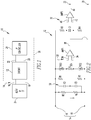
- Arrangement 10 includes a circuit 12 having an input pair 14 consisting of a first input 16 and a second input 18. Circuit 12 further includes a first output 20 and a second output 22. Current sensing arrangement 10 further includes a current sensor 24 connected to input pair 14 which is structured to provide an output dependent on a current sensed by current sensor 24.
- current sensor 24 is one of either a di/dt sensor (di/dt) or a current transformer (CT).
- Circuit 12 is configured to receive the output from the one of the di/dt sensor or the current transformer which is connected to input pair 14 and to provide an output signal which corresponds to the input received from the di/dt sensor or the current transformer which is connected to input pair 14.
- the output signal is provided via either first output 20 or second output 22, depending on which of the di/dt sensor or the current transformer is connected to input pair 14.
- a given current sensing arrangement 10 in accordance with the disclosed concept may include either of a di/dt sensor or a current transformer connected to input pair 14 at a given time, but not both of a di/dt sensor and current transformer connected simultaneously.
- current sensing arrangement 10 further includes a microcontroller 26 which is connected to first output 20 and second output 22 of circuit 12.
- Microcontroller 26 may be any suitable processing device and is adapted and programmed to determine which of the first output 20 and second output 22 from circuit 12 corresponds to either of the di/dt sensor or current transformer connected to input pair 14, as will be discussed below.
- circuit 12 may be a standalone unit which may be connected to a suitable microcontroller 26 and which may have current sensor 24 coupled thereto.
- circuit 12 and microcontroller 26 may be included as part of a circuit breaker 28, such as schematically shown partially in Figure 1 in dashed line.
- current sensor 24 may be readily connected to input pair 14 which may be provided generally on a housing (not numbered) of circuit breaker 28.
- circuit 12 includes an input pair 14 having a first input 16 and a second input 18, as well as a first output 20 and a second output 22.
- Circuit 12 further includes a current transformer input circuit, shown generally at 30, connected between first input 16 and second input 18, as well as a di/dt sensor input circuit, shown generally at 32, which likewise is connected between first input 16 and second input 18 in a parallel arrangement with current transformer input circuit 30.
- Current transformer input circuit 30 is configured to receive output from a current transformer employed as current sensor 24 connected to input pair 14 and to output a signal representative of the current sensed thereby via first output 20 for use by a further electrical component, e.g., without limitation, microcontroller 26.
- Current transformer input circuit 30 includes: a sense resistor Rsen connected between first input 16 and second input 18; a first resistor R1 connected in parallel with a first transient voltage suppression diode TVS1 connected between first input 16 and sense resistor Rsen; and a second resistor R2 connected in parallel with a second transient voltage suppression diode TVS2 connected between sense resistor Rsen and second input 18.
- Current transformer input circuit 30 further includes a first differential amplifier AMP1 having a first input 34 connected on a first side of sense resistor Rsen and a second input 36 connected on an opposite second side of sense resistor Rsen so as to measure the voltage across sense resistor Rsen.
- An output 38 from first differential amplifier AMP1 is connected to first output 20 of circuit 12.
- the example current transformer input circuit 30 shown in Figure 2 is a balanced configuration that takes advantage of the fact that current transformers will provide primary proportional current to higher voltage, non-linear loads.
- Transient voltage suppression diodes TVS 1 and TVS2 (or the alternative zener diodes discussed above), have little effect on the secondary current from a current transformer connected to input pair 14. If the burden on the current transformer created by the transient voltage suppression diodes or the zener diodes is too great, it is possible to add a switch (FET) to insert the burden resistors directly across the current transformer.
- FET switch
- An example of such alternate arrangement is discussed further below in conjunction with Figure 4 . In this case, output from a di/dt sensor utilized as current sensor 24 should be kept well below one diode drop (or below PS voltage if an analog switch is used).
- di/dt sensor input circuit 32 is configured to receive the output from a di/dt sensor employed as current sensor 24 connected to input pair 14 and to output a signal representative of the current sensed thereby via second output 22 for use by a further electrical component, e.g., without limitation, microcontroller 26.
- the di/dt sensor input circuit 32 includes: a first capacitor C1 connected between first input 16 and second input 18 of input pair 14, a third resistor R3 connected between first input 16 and first capacitor C1, and a fourth resistor R4 connected between first capacitor C1 and second input 18.
- the di/dt sensor input circuit 32 further includes a second differential amplifier AMP2 having a first input 40 connected on a first side of first capacitor C1 and a second input 42 connected on an opposite second side of first capacitor C1 so as to measure the voltage across first capacitor C1.
- An output 44 from the second differential amplifier AMP2 is connected to second output 22 of circuit 12.
- di/dt sensor input circuit 32 is a balanced configuration. As previously mentioned, output voltages from a di/dt sensor are generally less than what can be produced by a current transformer for equivalent primary currents. Normal operating currents through a di/dt sensor will not produce a voltage anywhere near large enough to cause current to flow in the transient voltage suppression diodes TVS1 and TVS2 or current transformer input circuit 30. Accordingly, transient voltage suppression diodes TVS1 and TVS2 therefore appear as a high impedance to a di/dt sensor connected to input pair 14 and thus have no impact on output from the di/dt sensor.
- third and fourth resistors R3 and R4 and first capacitor C1 form a passive integration circuit that functions independent of the state of the power supplies for second differential amplifier AMP2 (as well as microcontroller 26).
- This configuration has some advantages in circuit breaker applications although other interfaces without passive integration are possible.
- circuit 10 further includes a third circuit, generally shown at 50, which is connected between first input 16 and second input 18 in a parallel arrangement with current transformer input circuit 30 and di/dt sensor input circuit 32.
- Third circuit 50 includes a ground connected between first input 16 and second input 18; a fifth resistor R5 connected in parallel with a second capacitor C2 connected between first input 16 and the ground; and a sixth resistor R6 connected in parallel with a third capacitor C3 connected between the ground and second input 18.
- third circuit 50 serves as a path to ground for input current to amplifiers AMP1 and AMP2 while second and third capacitors C2 and C3 serve to roll off high-frequency noise.
- first and second resistors R1 and R2 having a resistance of 100k ⁇ ; a sense resistor Rsen having a resistance of 1 ⁇ , and transient voltage suppression diodes TVS 1 and TVS2 of 5.1v were employed in current transformer input circuit 30.
- third and fourth resistors R3 and R4 having a resistance of 200k ⁇ along with a 0.1 ⁇ F first capacitor C1 were employed in di/dt sensor input circuit 32.
- fifth and sixth resistors R5 and R6 having a resistance in the range of 10k ⁇ - 100k ⁇ were employed along with second and third capacitors C3 and C4 in the range of 100pF - 1000pF in third circuit 50. It is to be appreciated that such example values are provided for exemplary purposes only and that other values may be employed without varying from the scope of the disclosed concept.
- Table 1 summarizes the outputs 20, 22 that can be expected from circuits 30 and 32.
- Automatic sensing can be considered in a microcontroller, such as microcontroller 26, that looks for saturated outputs on second output 22 from di/dt sensor input circuit 32 paired with small, 'reasonable' levels on first output 20 from current transformer input circuit 30.
- a current transformer utilized as current sensor 24 connected to input pair 14 of circuit 12.
- the output from second output 22 from di/dt sensor input circuit 32 is 'reasonable' and the output from first output 20 from current transformer input circuit 20 is at or near zero, then a di/dt sensor is being utilized as current sensor 24 connected to input pair 14 of circuit 12.
- connection of a current transformer to input pair 14 will result in saturation of output 44 of second amplifier AMP2 for very small primary currents. This is because current will flow through the diodes TVS 1 and TVS2 resulting in what would appear to be very large di/dt sensor signals. Meanwhile, output 38 from first amplifier AMP1 would appear normal.
- the connection of a di/dt sensor to input pair 14 would result in normal appearing signals from second amplifier AMP2 and a nearly zero signal from first amplifier AMP1.
- the difficult case is when a di/dt sensor is connected and a large fault occurs, rms signal levels from the first and second amplifiers AMP1 and AMP2 could duplicate those seen for smaller currents when a current transformer is connected to input pair 14.
- the circuit 10 is self-protecting in that it will not allow large voltages to be generated across a connected current transformer no matter the configuration - in fact hardware configuration is not altered for different types of coil.
- One must watch that the current transformers employed are not significantly impacted by the zener burden put on them by the transient voltage suppression diodes TVS1 and TVS2.
- the design allows for a fair amount of flexibility in the choice of the transient voltage suppression diodes TVS 1 and TVS2 utilized. Such values must only be large enough to assure that they do not 'turn on' under normal di/dt sensor operation as such occurrence would lead to current reading errors.
- the voltage of the transient voltage suppression diodes TVS 1 and TVS2 may be lowered to the point where the voltages created by the di/dt sensor at maximum current are lower than the total voltage of the transient voltage suppression diodes TVS1 and TVS2. Meeting this criteria assures that transient voltage suppression diodes TVS1 and TVS2 always appear as a high impedance to the di/dt sensor.
- the 12V string described above would be suitable for peak currents below 40kA or 28kA rms.
- the use case for these sensors is normally for ground or zero sequence sensing, which is often limited to 1200A rms max.
- transient voltage suppression diodes TVS1 and TVS2 are quite conservative. If 1200A rms is used as the max, then the transient voltage suppression diodes TVS 1 and TVS2 could be replaced by simple silicon diodes. It is to be appreciated that whatever diodes are selected they must be able to handle the maximum fault currents expected for the particular application. Depending on the current transformer this could reach many amps for a half cycle.
- the example amplifiers AMP1 and AMP2 have differential inputs. This keeps the two lines from the coil balanced. It is possible to create a circuit with similar performance without balanced inputs. However the voltage across the current transformer must be symmetric. That means that the positive voltage across the current transformer must be equal the negative voltage across the current transformer. Failure to do so will result in the current transformer drifting toward saturation and poor performance.
- the selected amplifiers AMP1 and AMP2 above require that the common mode voltage be kept within the power supply range of the amp. Other amplifier selections do not have this requirement.
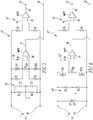
- circuit 12' is the same as circuit 12 previously discussed in conjunction with Figure 2 , except circuit 12' includes a di/dt sensor input circuit 32' which does not include a capacitor such as capacitor C1 of FIG. 2 . Accordingly, in di/dt sensor input circuit 32', first input 40 of second amplifier AMP2 is connected to first input 16 of circuit 12' via third resistor R3 and second input of second amplifier AMP2 is connected to second input 18 of circuit 12' via fourth resistor R4. In this arrangement the integration of the di/dt sensor signal can be performed digitally by a microcontroller. Digital integration eliminates concerns over drift and tolerance of the discrete resistors and capacitors used in the arrangement of Figure 2 .
- FIG 4 is a circuit diagram of yet another example circuit 12" in accordance with an example embodiment of the disclosed concept which may be employed in the current sensing arrangement 10 of Figure 1 .
- Circuit 12" includes a di/dt sensor input circuit 32' the same as circuit 12' previously discussed in conjunction with Figure 3 .
- circuit 12" includes a current transformer input circuit 30" which includes a first field effect transistor FET1 connected between first input 16 and sense resistor Rsen (instead of first resistor R1 and first transient voltage suppression diode TVS1) and a second field effect transistor FET2 connected between sense resistor Rsen and second input 18 (instead of second resistor R2 and second transient voltage suppression diode TVS2).
- first and second field effect transistors FET1 and FET2 When a di/dt sensor is connected to inputs 16 and 18, first and second field effect transistors FET1 and FET2 would be off. By turning on first and second field effect transistors FET1 and FET2, the voltage that a current transformer connected to inputs 16 and 18 must drive is substantially reduced. This reduction in burden voltage improves the linearity of the current transformer, making this arrangement more suitable for metering applications.
- circuit 12" includes a third circuit 50" which, similar to third circuit 50, includes a ground connected between first input 16 and second input 18, fifth resistor R5 connected between first input 16 and the ground, sixth resistor R6 connected between the ground and second input 18.
- third circuit 50" does not include second or third capacitors C2 or C3.
- third circuit 50" further includes a third zener diode Z3 and a fourth zener diode Z4 connected opposing in series between first input 16 and second input 18 in parallel with the arrangement of the ground and fifth and sixth resistors R5 and R6.
- third circuit 50" serves as a path to ground for input current to second amplifier AMP2 while third and fourth zener diodes Z3 and Z4 limit current transformer voltages in the case where a current transformer is operated without first field effect transistor FET1 and second field effect transistor FET2 turned on.
- Figure 5 is a circuit diagram of a further example circuit 12"' in accordance with an example embodiment of the disclosed concept which may be employed in a current sensing arrangement similar to that of Figure 1 .
- circuit 12' includes a di/dt sensor input circuit 32' having output 44 from second amplifier AMP2 connected to an output 22 of circuit 12'".
- circuit 12' unlike circuits 12, 12' and 12", previously discussed in conjunction with Figures 2-4 , which included two outputs (i.e., first and second outputs 20 and 22), circuit 12'" only utilizes a single output, i.e., output 22.
- circuit 12"' utilizes a current transformer input circuit 30'" which includes first field effect transistor FET1 connected between first input 16 and sense resistor Rsen, and second field effect transistor FET2 connected between sense resistor Rsen and second input 18.
- current transformer input circuit 30' does not include first amplifier AMP1.
- first and second field effect transistors FET1 and FET2 should be chosen such that their Rds on value is small compared to Rsense so that Rds on variations with temperature or Gate-Source voltage do not impact performance.
- Circuit 12'” also includes third circuit 50" such as described in conjunction with Figure 4 and arranged in the same manner. The arrangement of Figure 5 requires only a single interface to the microcontroller which is important in space constrained or pin-limited applications.
Landscapes
- Physics & Mathematics (AREA)
- General Physics & Mathematics (AREA)
- Engineering & Computer Science (AREA)
- Power Engineering (AREA)
- Automation & Control Theory (AREA)
- Measurement Of Current Or Voltage (AREA)
- Keying Circuit Devices (AREA)
Abstract
Description
- The disclosed concept relates generally to arrangements for sensing current, and, more particularly, to arrangements for sensing current used in conjunction with circuit breakers. The disclosed concept also relates to circuit breakers including such arrangements.
- In circuit breakers and other applications, it is often desirable or necessary to connect a current sensor mounted external the breaker. Such a sensor may be used to sense an external neutral current, a ground current, or wrapped around multiple conductors to sense a current imbalance. Traditionally, the application was filled by current transformers. However, recently Rogowski coils have become more popular for several reasons: they can be made smaller and lighter than current transformers; they can be more easily made in split core configurations providing for a simpler installation; and they do not suffer from the effects of saturation.
- The outputs of current transformers and Rogowski coils are quite different. Current transformers produce output currents proportional to their primary currents. The proportionality of this current is generally quite constant even when burdened by higher impedance, nonlinear loads.
- On the other hand, di/dt sensors, e.g., without limitation, Rogowski coils, produce voltages proportional to sensed di/dt. The voltages are typically small, around 100µV/A, with their function being maintained only for relatively high impedance loads.
- For ease of use by an end user, it would be preferable to handle these two different types of sensors outputs with a single input so as to eliminate the need to provide multiple input pairs for such sensors on circuit breakers and therewith also reduce/eliminate any potential errors in connecting of either of such sensors by an end user to a circuit breaker.
- These needs and others are met by embodiments of the disclosed concept, in which a circuit is adapted to receive input from either a current transformer or a di/dt sensor and to output a signal corresponding to the input.
- In accordance with one aspect of the disclosed concept, a circuit comprises: an input pair having a first input and a second input; a first output; a second output; a current transformer input circuit connected between the first input and the second input; and a di/dt sensor input circuit connected between the first input and the second input, wherein the current transformer input circuit is configured to receive output from a current transformer connected to the input pair and to output a signal representative of the current sensed thereby via the first output, and wherein the di/dt sensor input circuit is configured to receive output from a di/dt sensor connected to the input pair and to output a signal representative of the current or time rate of change of the current sensed thereby via the second output.
- The current transformer input circuit and the di/dt sensor input circuit may be connected in a parallel arrangement.
- The circuit may further comprise: a third circuit connected between the first input and the second input, the third circuit comprising: a ground connected between the first input and the second input, a fifth resistor connected in parallel with a second capacitor connected between the first input and the ground, and a sixth resistor connected in parallel with a third capacitor connected between the ground and the second input.
- The current transformer input circuit, the di/dt sensor input circuit, and the third circuit may be connected in a parallel arrangement between the first input and the second input.
- The circuit may further comprise: a third circuit connected between the first input and the second input, the third circuit comprising: a first arrangement comprising: a ground connected between the first input and the second input; a fifth resistor connected between the first input and the ground; and a sixth resistor connected between the ground and the second input; and a second arrangement comprising a third zener diode and a fourth zener diode connected opposing in series between the first input and the second input.
- The current transformer input circuit may comprise: a sense resistor connected between the first input and the second input; a first resistor connected in parallel with one of either a first transient voltage suppression diode or a first Zener diode connected between the first input and the sense resistor; a second resistor connected in parallel with another one of a second transient voltage suppression diode or a second Zener diode connected between the sense resistor and the second input; and a first amplifier having a first input connected on a first side of the sense resistor, a second input connected on an opposite second side of the sense resistor, and an output connected to the first output.
- The current transformer input circuit may comprise: a sense resistor connected between the first input and the second input; a first field effect transistor connected between the first input and the sense resistor; a second field effect transistor connected between the sense resistor and the second input; and a first amplifier having a first input connected on a first side of the sense resistor, a second input connected on an opposite second side of the sense resistor, and an output connected to the first output.
- The di/dt sensor input circuit may comprise: a first capacitor connected between the first input and the second input; a third resistor connected between the first input and the first capacitor; a fourth resistor connected between the first capacitor and the second input; and a second amplifier having a first input connected on a first side of the first capacitor and a second input connected on an opposite second side of the first capacitor, and an output connected to the second output.
- The di/dt sensor input circuit may comprise: a first capacitor connected between the first input and the second input; a third resistor connected between the first input and the first capacitor; a fourth resistor connected between the first capacitor and the second input; and a second amplifier having a first input connected on a first side of the first capacitor and a second input connected on an opposite second side of the first capacitor, and an output connected to the second output.
- The di/dt sensor input circuit may comprise: a second amplifier having a first input, a second input, and an output connected to the second output; a third resistor connected between the first input of the circuit and the first input of the second amplifier; and a fourth resistor connected between the second input of the circuit and the second input of the second amplifier.
- The di/dt sensor input circuit may comprise: a second amplifier having a first input, a second input, and an output connected to the second output; a third resistor connected between the first input of the circuit and the first input of the second amplifier; and a fourth resistor connected between the second input of the circuit and the second input of the second amplifier.
- The di/dt sensor input circuit may comprise: a second amplifier having a first input, a second input, and an output connected to the second output; a third resistor connected between the first input of the circuit and the first input of the second amplifier; and a fourth resistor connected between the second input of the circuit and the second input of the second amplifier.
- In accordance with another aspect of the disclosed concept, a circuit comprises: an input pair having a first input and a second input; an output; a first sensor input circuit connected between the first input and the second input, the first sensor input circuit comprising: a sense resistor connected between the first input and the second input; a first field effect transistor connected between the first input and the sense resistor; and a second field effect transistor connected between the sense resistor and the second input; and a second sensor input circuit connected between the first input and the second input, the second sensor input circuit comprising: an amplifier having a first input, a second input, and an output connected to the output of the circuit; a third resistor connected between the first input of the circuit and the first input of the amplifier; and a fourth resistor connected between the second input of the circuit and the second input of the amplifier, wherein the circuit is configured to receive output from one of either a current transformer or a di/dt sensor and output a signal representative of a current sensed by the one of either the current transformer or the di/dt sensor via the output.
- The circuit may further comprise: a third circuit connected between the first input and the second input, the third circuit comprising: a first arrangement comprising: a ground connected between the first input and the second input; a fifth resistor connected between the first input and the ground; and a sixth resistor connected between the ground and the second input; and a second arrangement comprising a third zener diode and a fourth zener diode connected opposing in series between the first input and the second input.
- In accordance with yet another aspect of the disclosed concept, a circuit breaker comprises: a circuit as previously recited; and a microcontroller connected to the first output and the second output of the circuit.
- The microcontroller may be adapted to automatically sense which output from the first output or the second output corresponds to a current sensed by a current sensor connected to the input pair.
- In accordance with a further aspect of the disclosed concept, a current sensing arrangement comprises: a circuit as previously recited; a current sensor structured to provide an output dependent on a sensed current, the current sensor connected to the input pair of the circuit; and a microcontroller connected to the first output and the second output of the circuit, wherein the current sensor is one of either a di/dt sensor or a current transformer; and wherein the circuit is configured to receive the output of the one of either the di/dt sensor or the current transformer which is connected to the input pair and provide an output signal which corresponds to the one of either the di/dt sensor or the current transformer via either the first output or the second output, dependent on which one of the di/dt sensor or the current transformer is connected to the input pair.
- A full understanding of the disclosed concept can be gained from the following description of the preferred embodiments when read in conjunction with the accompanying drawings in which:
-
Figure 1 is a block diagram of a current sensing arrangement in accordance with an example embodiment of the disclosed concept; -
Figure 2 is a circuit diagram of an example circuit in accordance with an example embodiment of the disclosed concept which may be employed in the current sensing arrangement ofFigure 1 ; -
Figure 3 is a circuit diagram of an example circuit in accordance with an example embodiment of the disclosed concept which may be employed in the current sensing arrangement ofFigure 1 ; -
Figure 4 is a circuit diagram of an example circuit in accordance with an example embodiment of the disclosed concept which may be employed in the current sensing arrangement ofFigure 1 ; and -
Figure 5 is a circuit diagram of an example circuit in accordance with an example embodiment of the disclosed concept which may be employed in a current sensing arrangement similar to that ofFigure 1 . - Directional phrases used herein, such as, for example, left, right, clockwise, counterclockwise and derivatives thereof, relate to the orientation of the elements shown in the drawings and are not limiting upon the claims unless expressly recited therein.
- As employed herein, the term "di/dt sensor" shall be used to refer to any device for sensing current which produces an output voltage which is proportional to the time rate of change of the current sensed by such device. For example, without limitation, a Rogowski coil is an example of a suitable di/dt sensor which may be employed in embodiments of the disclosed concept.
- As employed herein, the statement that two or more parts are "coupled" together shall mean that the parts are joined together either directly or joined through one or more intermediate parts.
- As employed herein, the statement that two or more parts are "connected" shall mean that the parts are joined either directly or through one or more intermediate parts in a manner such that an electrical pathway is formed through such parts.
- As employed herein, the term "number" shall mean one or an integer greater than one (i.e., a plurality).
- Referring to
Figure 1 , a block diagram of a current sensing arrangement 10 in accordance with an example embodiment of the disclosed concept is shown. Arrangement 10 includes acircuit 12 having aninput pair 14 consisting of afirst input 16 and asecond input 18.Circuit 12 further includes afirst output 20 and asecond output 22. Current sensing arrangement 10 further includes acurrent sensor 24 connected toinput pair 14 which is structured to provide an output dependent on a current sensed bycurrent sensor 24. In example embodiments of the disclosed concept,current sensor 24 is one of either a di/dt sensor (di/dt) or a current transformer (CT).Circuit 12 is configured to receive the output from the one of the di/dt sensor or the current transformer which is connected toinput pair 14 and to provide an output signal which corresponds to the input received from the di/dt sensor or the current transformer which is connected toinput pair 14. The output signal is provided via eitherfirst output 20 orsecond output 22, depending on which of the di/dt sensor or the current transformer is connected toinput pair 14. It is to be appreciated that a given current sensing arrangement 10 in accordance with the disclosed concept may include either of a di/dt sensor or a current transformer connected toinput pair 14 at a given time, but not both of a di/dt sensor and current transformer connected simultaneously. - Continuing to refer to
Figure 1 , current sensing arrangement 10 further includes amicrocontroller 26 which is connected tofirst output 20 andsecond output 22 ofcircuit 12.Microcontroller 26 may be any suitable processing device and is adapted and programmed to determine which of thefirst output 20 andsecond output 22 fromcircuit 12 corresponds to either of the di/dt sensor or current transformer connected toinput pair 14, as will be discussed below. - It is to be appreciated that
circuit 12 may be a standalone unit which may be connected to asuitable microcontroller 26 and which may havecurrent sensor 24 coupled thereto. Alternatively,circuit 12 andmicrocontroller 26 may be included as part of acircuit breaker 28, such as schematically shown partially inFigure 1 in dashed line. In such arrangement,current sensor 24 may be readily connected toinput pair 14 which may be provided generally on a housing (not numbered) ofcircuit breaker 28. - Referring now to
Figure 2 , a circuit diagram of anexample circuit 12 in accordance with an example embodiment of the disclosed concept which may be employed in the current sensing arrangement 10 ofFigure 1 is shown. As previously discussed in conjunction withFigure 1 ,circuit 12 includes aninput pair 14 having afirst input 16 and asecond input 18, as well as afirst output 20 and asecond output 22.Circuit 12 further includes a current transformer input circuit, shown generally at 30, connected betweenfirst input 16 andsecond input 18, as well as a di/dt sensor input circuit, shown generally at 32, which likewise is connected betweenfirst input 16 andsecond input 18 in a parallel arrangement with currenttransformer input circuit 30. - Current
transformer input circuit 30 is configured to receive output from a current transformer employed ascurrent sensor 24 connected toinput pair 14 and to output a signal representative of the current sensed thereby viafirst output 20 for use by a further electrical component, e.g., without limitation,microcontroller 26. Currenttransformer input circuit 30 includes: a sense resistor Rsen connected betweenfirst input 16 andsecond input 18; a first resistor R1 connected in parallel with a first transient voltage suppression diode TVS1 connected betweenfirst input 16 and sense resistor Rsen; and a second resistor R2 connected in parallel with a second transient voltage suppression diode TVS2 connected between sense resistor Rsen andsecond input 18. Alternatively, a first and a second Zener diode could be used in place of first and second transient voltage suppression diodes TVS1 and TVS2. Currenttransformer input circuit 30 further includes a first differential amplifier AMP1 having afirst input 34 connected on a first side of sense resistor Rsen and asecond input 36 connected on an opposite second side of sense resistor Rsen so as to measure the voltage across sense resistor Rsen. Anoutput 38 from first differential amplifier AMP1 is connected tofirst output 20 ofcircuit 12. - The example current
transformer input circuit 30 shown inFigure 2 is a balanced configuration that takes advantage of the fact that current transformers will provide primary proportional current to higher voltage, non-linear loads. Transient voltage suppression diodes TVS 1 and TVS2 (or the alternative zener diodes discussed above), have little effect on the secondary current from a current transformer connected to inputpair 14. If the burden on the current transformer created by the transient voltage suppression diodes or the zener diodes is too great, it is possible to add a switch (FET) to insert the burden resistors directly across the current transformer. An example of such alternate arrangement is discussed further below in conjunction withFigure 4 . In this case, output from a di/dt sensor utilized ascurrent sensor 24 should be kept well below one diode drop (or below PS voltage if an analog switch is used). - Continuing to refer to
Figure 2 , di/dtsensor input circuit 32 is configured to receive the output from a di/dt sensor employed ascurrent sensor 24 connected to inputpair 14 and to output a signal representative of the current sensed thereby viasecond output 22 for use by a further electrical component, e.g., without limitation,microcontroller 26. The di/dtsensor input circuit 32 includes: a first capacitor C1 connected betweenfirst input 16 andsecond input 18 ofinput pair 14, a third resistor R3 connected betweenfirst input 16 and first capacitor C1, and a fourth resistor R4 connected between first capacitor C1 andsecond input 18. The di/dtsensor input circuit 32 further includes a second differential amplifier AMP2 having afirst input 40 connected on a first side of first capacitor C1 and asecond input 42 connected on an opposite second side of first capacitor C1 so as to measure the voltage across first capacitor C1. Anoutput 44 from the second differential amplifier AMP2 is connected tosecond output 22 ofcircuit 12. - Similar to current
transformer input circuit 30, di/dtsensor input circuit 32 is a balanced configuration. As previously mentioned, output voltages from a di/dt sensor are generally less than what can be produced by a current transformer for equivalent primary currents. Normal operating currents through a di/dt sensor will not produce a voltage anywhere near large enough to cause current to flow in the transient voltage suppression diodes TVS1 and TVS2 or currenttransformer input circuit 30. Accordingly, transient voltage suppression diodes TVS1 and TVS2 therefore appear as a high impedance to a di/dt sensor connected to inputpair 14 and thus have no impact on output from the di/dt sensor. Meanwhile, the arrangement of third and fourth resistors R3 and R4 and first capacitor C1 form a passive integration circuit that functions independent of the state of the power supplies for second differential amplifier AMP2 (as well as microcontroller 26). This configuration has some advantages in circuit breaker applications although other interfaces without passive integration are possible. - Continuing to refer to
Figure 2 , circuit 10 further includes a third circuit, generally shown at 50, which is connected betweenfirst input 16 andsecond input 18 in a parallel arrangement with currenttransformer input circuit 30 and di/dtsensor input circuit 32.Third circuit 50 includes a ground connected betweenfirst input 16 andsecond input 18; a fifth resistor R5 connected in parallel with a second capacitor C2 connected betweenfirst input 16 and the ground; and a sixth resistor R6 connected in parallel with a third capacitor C3 connected between the ground andsecond input 18. In operation,third circuit 50 serves as a path to ground for input current to amplifiers AMP1 and AMP2 while second and third capacitors C2 and C3 serve to roll off high-frequency noise. - In one example embodiment of the concept illustrated in
Figure 2 , first and second resistors R1 and R2 having a resistance of 100kΩ; a sense resistor Rsen having a resistance of 1Ω, and transient voltage suppression diodes TVS 1 and TVS2 of 5.1v were employed in currenttransformer input circuit 30. In the same example embodiment, third and fourth resistors R3 and R4 having a resistance of 200kΩ along with a 0.1 µF first capacitor C1 were employed in di/dtsensor input circuit 32. Also in the same example embodiment, fifth and sixth resistors R5 and R6 having a resistance in the range of 10kΩ - 100kΩ were employed along with second and third capacitors C3 and C4 in the range of 100pF - 1000pF inthird circuit 50. It is to be appreciated that such example values are provided for exemplary purposes only and that other values may be employed without varying from the scope of the disclosed concept. - Table 1 below summarizes the
outputs circuits microcontroller 26, that looks for saturated outputs onsecond output 22 from di/dtsensor input circuit 32 paired with small, 'reasonable' levels onfirst output 20 from currenttransformer input circuit 30. Such a situation describes a current transformer utilized ascurrent sensor 24 connected to inputpair 14 ofcircuit 12. Conversely, if the output fromsecond output 22 from di/dtsensor input circuit 32 is 'reasonable' and the output fromfirst output 20 from currenttransformer input circuit 20 is at or near zero, then a di/dt sensor is being utilized ascurrent sensor 24 connected to inputpair 14 ofcircuit 12. As used herein, the term 'reasonable' would is used to indicate an rms value in the normal range of operation.Table 1. Comparison of current sensor input to, and outputs from example circuit Sensing device employed as current sensor 24First output 20Second output 22Current Transformer Saturated α sensed current di/dt sensor α sensed current ≈ 0 - For the design shown in
Figure 2 with the particular values described above, the connection of a current transformer to inputpair 14 will result in saturation ofoutput 44 of second amplifier AMP2 for very small primary currents. This is because current will flow through the diodes TVS 1 and TVS2 resulting in what would appear to be very large di/dt sensor signals. Meanwhile,output 38 from first amplifier AMP1 would appear normal. The connection of a di/dt sensor to inputpair 14 would result in normal appearing signals from second amplifier AMP2 and a nearly zero signal from first amplifier AMP1. The difficult case is when a di/dt sensor is connected and a large fault occurs, rms signal levels from the first and second amplifiers AMP1 and AMP2 could duplicate those seen for smaller currents when a current transformer is connected to inputpair 14. When looked at in conjunction with the phase currents, proper selection can be made. Additionally a sample by sample comparison can be done. With a di/dt sensor connected to inputpair 14, even at the highest fault currents, a substantial portion of the half cycle on first amplifier AMP1 will be zero. - It is to be appreciated that the circuit 10 is self-protecting in that it will not allow large voltages to be generated across a connected current transformer no matter the configuration - in fact hardware configuration is not altered for different types of coil. One must watch that the current transformers employed are not significantly impacted by the zener burden put on them by the transient voltage suppression diodes TVS1 and TVS2. The design allows for a fair amount of flexibility in the choice of the transient voltage suppression diodes TVS 1 and TVS2 utilized. Such values must only be large enough to assure that they do not 'turn on' under normal di/dt sensor operation as such occurrence would lead to current reading errors.
- Current transformers utilized must be capable of driving the voltages of the transient voltage suppression diodes TVS1 and TVS2 selected. In the example embodiment utilizing components with the values provided above, such voltage is 2 x 5.1V + 2 x Vf + (voltage across the sense resistor). This will be on the order of 12V. In this case 'driving the voltages' means that the current transformer should be able to provide rms current to within approximately 5% of the desired value of Iprimary/N. In other words the core of the current transformer should not saturate when burdened by this voltage.
- To lower the burden on the current transformer, the voltage of the transient voltage suppression diodes TVS 1 and TVS2 may be lowered to the point where the voltages created by the di/dt sensor at maximum current are lower than the total voltage of the transient voltage suppression diodes TVS1 and TVS2. Meeting this criteria assures that transient voltage suppression diodes TVS1 and TVS2 always appear as a high impedance to the di/dt sensor. For a typical di/dt sensor with a sensitivity of around 300µV/A. The 12V string described above would be suitable for peak currents below 40kA or 28kA rms. The use case for these sensors is normally for ground or zero sequence sensing, which is often limited to 1200A rms max. So the selected transient voltage suppression diodes TVS1 and TVS2 are quite conservative. If 1200A rms is used as the max, then the transient voltage suppression diodes TVS 1 and TVS2 could be replaced by simple silicon diodes. It is to be appreciated that whatever diodes are selected they must be able to handle the maximum fault currents expected for the particular application. Depending on the current transformer this could reach many amps for a half cycle.
- The example amplifiers AMP1 and AMP2 have differential inputs. This keeps the two lines from the coil balanced. It is possible to create a circuit with similar performance without balanced inputs. However the voltage across the current transformer must be symmetric. That means that the positive voltage across the current transformer must be equal the negative voltage across the current transformer. Failure to do so will result in the current transformer drifting toward saturation and poor performance. The selected amplifiers AMP1 and AMP2 above require that the common mode voltage be kept within the power supply range of the amp. Other amplifier selections do not have this requirement.
- Referring now to
Figure 3 , a circuit diagram of another example circuit 12' in accordance with an example of the disclosed concept which may be employed in the current sensing arrangement 10 ofFigure 1 is shown. Circuit 12' is the same ascircuit 12 previously discussed in conjunction withFigure 2 , except circuit 12' includes a di/dt sensor input circuit 32' which does not include a capacitor such as capacitor C1 ofFIG. 2 . Accordingly, in di/dt sensor input circuit 32',first input 40 of second amplifier AMP2 is connected tofirst input 16 of circuit 12' via third resistor R3 and second input of second amplifier AMP2 is connected tosecond input 18 of circuit 12' via fourth resistor R4. In this arrangement the integration of the di/dt sensor signal can be performed digitally by a microcontroller. Digital integration eliminates concerns over drift and tolerance of the discrete resistors and capacitors used in the arrangement ofFigure 2 . -
Figure 4 is a circuit diagram of yet anotherexample circuit 12" in accordance with an example embodiment of the disclosed concept which may be employed in the current sensing arrangement 10 ofFigure 1 .Circuit 12" includes a di/dt sensor input circuit 32' the same as circuit 12' previously discussed in conjunction withFigure 3 . Unlike circuit 12',circuit 12" includes a currenttransformer input circuit 30" which includes a first field effect transistor FET1 connected betweenfirst input 16 and sense resistor Rsen (instead of first resistor R1 and first transient voltage suppression diode TVS1) and a second field effect transistor FET2 connected between sense resistor Rsen and second input 18 (instead of second resistor R2 and second transient voltage suppression diode TVS2). When a di/dt sensor is connected toinputs inputs - Continuing to refer to
Figure 4 , additionally, unlike circuit 12',circuit 12" includes athird circuit 50" which, similar tothird circuit 50, includes a ground connected betweenfirst input 16 andsecond input 18, fifth resistor R5 connected betweenfirst input 16 and the ground, sixth resistor R6 connected between the ground andsecond input 18. Unlikethird circuit 50 ofcircuits 12 and 12' ofFigures 2 and3 ,third circuit 50" does not include second or third capacitors C2 or C3. Also, unlikethird circuit 50 ofcircuits 12 and 12' ofFigures 2 and3 ,third circuit 50" further includes a third zener diode Z3 and a fourth zener diode Z4 connected opposing in series betweenfirst input 16 andsecond input 18 in parallel with the arrangement of the ground and fifth and sixth resistors R5 and R6. In operation,third circuit 50" serves as a path to ground for input current to second amplifier AMP2 while third and fourth zener diodes Z3 and Z4 limit current transformer voltages in the case where a current transformer is operated without first field effect transistor FET1 and second field effect transistor FET2 turned on. -
Figure 5 is a circuit diagram of afurther example circuit 12"' in accordance with an example embodiment of the disclosed concept which may be employed in a current sensing arrangement similar to that ofFigure 1 . Similar tocircuits 12' and 12", circuit 12'" includes a di/dt sensor input circuit 32' havingoutput 44 from second amplifier AMP2 connected to anoutput 22 of circuit 12'". However, unlikecircuits Figures 2-4 , which included two outputs (i.e., first andsecond outputs 20 and 22), circuit 12'" only utilizes a single output, i.e.,output 22. Similar tocircuit 12" ofFigure 4 ,circuit 12"' utilizes a current transformer input circuit 30'" which includes first field effect transistor FET1 connected betweenfirst input 16 and sense resistor Rsen, and second field effect transistor FET2 connected between sense resistor Rsen andsecond input 18. However, unlike the arrangement shown inFigure 4 , current transformer input circuit 30'" does not include first amplifier AMP1. In this arrangement first and second field effect transistors FET1 and FET2 should be chosen such that their Rds on value is small compared to Rsense so that Rds on variations with temperature or Gate-Source voltage do not impact performance. Circuit 12'" also includesthird circuit 50" such as described in conjunction withFigure 4 and arranged in the same manner. The arrangement ofFigure 5 requires only a single interface to the microcontroller which is important in space constrained or pin-limited applications. - While specific embodiments of the disclosed concept have been described in detail, it will be appreciated by those skilled in the art that various modifications and alternatives to those details could be developed in light of the overall teachings of the disclosure. Accordingly, the particular arrangements disclosed are meant to be illustrative only and not limiting as to the scope of the disclosed concept which is to be given the full breadth of the claims appended and any and all equivalents thereof.
Claims (15)
- A circuit comprising:an input pair having a first input and a second input;a first output;a second output;a current transformer input circuit connected between the first input and the second input; anda di/dt sensor input circuit connected between the first input and the second input,wherein the current transformer input circuit is configured to receive output from a current transformer connected to the input pair and to output a signal representative of the current sensed thereby via the first output, andwherein the di/dt sensor input circuit is configured to receive output from a di/dt sensor connected to the input pair and to output a signal representative of the current or time rate of change of the current sensed thereby via the second output.
- The circuit of claim 1, wherein the current transformer input circuit and the di/dt sensor input circuit are connected in a parallel arrangement.
- The circuit of claim 1, further comprising:
a third circuit connected between the first input and the second input, the third circuit comprising:a ground connected between the first input and the second input,a fifth resistor connected in parallel with a second capacitor connected between the first input and the ground, anda sixth resistor connected in parallel with a third capacitor connected between the ground and the second input. - The circuit of claim 3, wherein the current transformer input circuit, the di/dt sensor input circuit, and the third circuit are connected in a parallel arrangement between the first input and the second input.
- The circuit of claim 1, further comprising: a third circuit connected between the first input and the second input, the third circuit comprising:a first arrangement comprising:a ground connected between the first input and the second input;a fifth resistor connected between the first input and the ground; anda sixth resistor connected between the ground and the second input; anda second arrangement comprising a third zener diode and a fourth zener diode connected opposing in series between the first input and the second input.
- The circuit of claim 1, wherein the current transformer input circuit comprises:a sense resistor connected between the first input and the second input;a first resistor connected in parallel with one of either a first transient voltage suppression diode or a first Zener diode connected between the first input and the sense resistor;a second resistor connected in parallel with another one of a second transient voltage suppression diode or a second Zener diode connected between the sense resistor and the second input; anda first amplifier having a first input connected on a first side of the sense resistor, a second input connected on an opposite second side of the sense resistor, and an output connected to the first output.
- The circuit of claim 1, wherein the current transformer input circuit comprises:a sense resistor connected between the first input and the second input;a first field effect transistor connected between the first input and the sense resistor;a second field effect transistor connected between the sense resistor and the second input; anda first amplifier having a first input connected on a first side of the sense resistor, a second input connected on an opposite second side of the sense resistor, and an output connected to the first output.
- The circuit of either of claims 1 or 6, wherein the di/dt sensor input circuit comprises:a first capacitor connected between the first input and the second input;a third resistor connected between the first input and the first capacitor;a fourth resistor connected between the first capacitor and the second input; anda second amplifier having a first input connected on a first side of the first capacitor and a second input connected on an opposite second side of the first capacitor, and an output connected to the second output.
- The circuit of either of claims 1 or 6, wherein the di/dt sensor input circuit comprises:a second amplifier having a first input, a second input, and an output connected to the second output;a third resistor connected between the first input of the circuit and the first input of the second amplifier; anda fourth resistor connected between the second input of the circuit and the second input of the second amplifier.
- The circuit of claim 7, wherein the di/dt sensor input circuit comprises:a second amplifier having a first input, a second input, and an output connected to the second output;a third resistor connected between the first input of the circuit and the first input of the second amplifier; anda fourth resistor connected between the second input of the circuit and the second input of the second amplifier.
- A circuit comprising:an input pair having a first input and a second input;an output;a first sensor input circuit connected between the first input and the second input, the first sensor input circuit comprising:a sense resistor connected between the first input and the second input;a first field effect transistor connected between the first input and the sense resistor; anda second field effect transistor connected between the sense resistor and the second input; anda second sensor input circuit connected between the first input and the second input, the second sensor input circuit comprising:an amplifier having a first input, a second input, and an output connected to the output of the circuit;a third resistor connected between the first input of the circuit and the first input of the amplifier; anda fourth resistor connected between the second input of the circuit and the second input of the amplifier,wherein the circuit is configured to receive output from one of either a current transformer or a di/dt sensor and output a signal representative of a current sensed by the one of either the current transformer or the di/dt sensor via the output.
- The circuit of claim 11, further comprising:
a third circuit connected between the first input and the second input, the third circuit comprising:a first arrangement comprising:a ground connected between the first input and the second input;a fifth resistor connected between the first input and the ground; anda sixth resistor connected between the ground and the second input; anda second arrangement comprising a third zener diode and a fourth zener diode connected opposing in series between the first input and the second input. - A circuit breaker comprising:a circuit as recited in any of the preceding claims; anda microcontroller connected to the first output and the second output of the circuit.
- The circuit breaker of claim 13, wherein the microcontroller is adapted to automatically sense which output from the first output or the second output corresponds to a current sensed by a current sensor connected to the input pair.
- A current sensing arrangement comprising:a circuit as recited in any of claims 1-12;a current sensor structured to provide an output dependent on a sensed current, the current sensor connected to the input pair of the circuit; anda microcontroller connected to the first output and the second output of the circuit,wherein the current sensor is one of either a di/dt sensor or a current transformer, andwherein the circuit is configured to receive the output of the one of either the di/dt sensor or the current transformer which is connected to the input pair and provide an output signal which corresponds to the one of either the di/dt sensor or the current transformer via either the first output or the second output, dependent on which one of the di/dt sensor or the current transformer is connected to the input pair.
Applications Claiming Priority (1)
| Application Number | Priority Date | Filing Date | Title |
|---|---|---|---|
| US16/197,504 US10840012B2 (en) | 2018-11-21 | 2018-11-21 | Single input circuit for receiving output from a di/dt sensor or current transformer and circuit breaker including same |
Publications (3)
| Publication Number | Publication Date |
|---|---|
| EP3657179A2 true EP3657179A2 (en) | 2020-05-27 |
| EP3657179A3 EP3657179A3 (en) | 2020-06-10 |
| EP3657179B1 EP3657179B1 (en) | 2023-04-19 |
Family
ID=68581494
Family Applications (1)
| Application Number | Title | Priority Date | Filing Date |
|---|---|---|---|
| EP19209007.4A Active EP3657179B1 (en) | 2018-11-21 | 2019-11-13 | Single input circuit for receiving output from a di/dt sensor or current transformer and circuit breaker including same |
Country Status (3)
| Country | Link |
|---|---|
| US (1) | US10840012B2 (en) |
| EP (1) | EP3657179B1 (en) |
| CN (1) | CN111208752B (en) |
Families Citing this family (2)
| Publication number | Priority date | Publication date | Assignee | Title |
|---|---|---|---|---|
| JP2021175124A (en) * | 2020-04-28 | 2021-11-01 | キオクシア株式会社 | Semiconductor integrated circuits and semiconductor storage devices |
| US20220181866A1 (en) | 2020-12-08 | 2022-06-09 | S&C Electric Company | Method for fast-detection of peak fault current |
Family Cites Families (19)
| Publication number | Priority date | Publication date | Assignee | Title |
|---|---|---|---|---|
| US3662218A (en) * | 1970-06-19 | 1972-05-09 | George A Whitlow | Ground fault interruptor circuit |
| US3815011A (en) * | 1973-03-30 | 1974-06-04 | Gen Electric | Current transformer terminated by active load elements for providing phase-inverted signals |
| US4713598A (en) * | 1986-10-29 | 1987-12-15 | Rca Corporation | Power supply associated with AC line relay switch |
| DE29622948U1 (en) | 1996-05-21 | 1997-09-25 | Siemens AG, 80333 München | Current detection device |
| WO1998016839A1 (en) | 1996-10-14 | 1998-04-23 | Siemens Aktiengesellschaft | Method and device for measuring current |
| US6987389B1 (en) * | 2000-11-14 | 2006-01-17 | Pass & Seymour, Inc. | Upstream/downstream arc fault discriminator |
| US6577484B1 (en) * | 2000-12-12 | 2003-06-10 | Pass & Seymour, Inc. | Arc fault detector device utilizing the di/dt and 60 Hz components of an arcing waveform |
| US6678136B2 (en) * | 2001-03-01 | 2004-01-13 | Hitachi, Ltd. | Protective relay apparatus |
| JP2005003601A (en) * | 2003-06-13 | 2005-01-06 | Fuji Electric Holdings Co Ltd | Hybrid sensor |
| FR2932568B1 (en) * | 2008-06-11 | 2010-06-11 | Schneider Electric Ind Sas | CURRENT MEASURING DEVICE AND PROCESSING UNIT COMPRISING SUCH A DEVICE |
| CN201589808U (en) * | 2009-12-11 | 2010-09-22 | 杭州雷盾电子设备有限公司 | Striking current recording instrument |
| US8611062B2 (en) * | 2010-05-13 | 2013-12-17 | Transtector Systems, Inc. | Surge current sensor and surge protection system including the same |
| KR101013064B1 (en) | 2010-08-20 | 2011-02-14 | 대동전자(주) | Switchboard equipped with double combination CT device and electronic controller |
| CN102818927B (en) * | 2012-06-29 | 2014-09-03 | 西安交通大学 | Measuring device and measuring method of reverse small current in direct current distribution system |
| US9276393B2 (en) * | 2012-10-01 | 2016-03-01 | Leviton Manufacturing Co., Inc. | Processor-based circuit interrupting devices |
| US9606146B2 (en) * | 2014-09-25 | 2017-03-28 | Fluke Corporation | Wireless rogowski coil system |
| CN204595059U (en) * | 2015-05-13 | 2015-08-26 | 中国人民解放军理工大学 | High tower lightning current measuring device |
| US9689900B1 (en) * | 2015-12-14 | 2017-06-27 | Keysight Technologies, Inc. | Current sensing circuit |
| CN108732414B (en) * | 2017-04-21 | 2021-03-16 | 西门子公司 | Current sensors and circuit breakers |
-
2018
- 2018-11-21 US US16/197,504 patent/US10840012B2/en active Active
-
2019
- 2019-11-04 CN CN201911068603.4A patent/CN111208752B/en active Active
- 2019-11-13 EP EP19209007.4A patent/EP3657179B1/en active Active
Also Published As
| Publication number | Publication date |
|---|---|
| US10840012B2 (en) | 2020-11-17 |
| US20200161045A1 (en) | 2020-05-21 |
| EP3657179B1 (en) | 2023-04-19 |
| CN111208752B (en) | 2024-01-16 |
| CN111208752A (en) | 2020-05-29 |
| EP3657179A3 (en) | 2020-06-10 |
Similar Documents
| Publication | Publication Date | Title |
|---|---|---|
| RU2114439C1 (en) | Current measuring instrument | |
| US20090312970A1 (en) | Current measuring device and processing unit comprising one such device | |
| US5508606A (en) | Direct current sensor | |
| US8143880B2 (en) | Dual-range measurement of electrical current | |
| JP2019530278A (en) | High voltage bootstrap sampling circuit | |
| EP3657179B1 (en) | Single input circuit for receiving output from a di/dt sensor or current transformer and circuit breaker including same | |
| US11943853B2 (en) | Full voltage sampling circuit, driving chip, LED driving circuit and sampling method | |
| US3895263A (en) | Grounded neutral detector drive circuit for two pole ground fault interrupter | |
| US5373410A (en) | Single string resistive divider network for a digital multimeter | |
| EP0789458A1 (en) | Circuit with overload current protection for power transistors | |
| US7928722B2 (en) | Apparatus and method for voltage sensing in electrical metering systems | |
| CA2689788C (en) | Matching turns ratio and resistance ratio in a transformer having a multilayer winding | |
| JP3221128B2 (en) | Current detector | |
| GB2026706A (en) | Current Sensor with Switchable Range-changing Resistor | |
| US20180247931A1 (en) | Voltage balanced stacked clamp | |
| US20030184940A1 (en) | Trip unit input method and device using a multiple conductor current transformer | |
| US4268885A (en) | GFI Sensor circuit | |
| US5614832A (en) | High voltage protected ohmmeter | |
| US3662218A (en) | Ground fault interruptor circuit | |
| US3172038A (en) | Double bridge circuit for measuring resistance of energized alternating current apparatus | |
| WO1996026567A1 (en) | An earth leakage detector circuit | |
| US5952855A (en) | Circuit with multiple output voltages for multiple analog to digital converters | |
| GB952998A (en) | Improvements relating to differential amplifiers | |
| US5719489A (en) | Apparatus for determining load currents | |
| US4922123A (en) | Supply circuit for a hall sensor multiplication circuit |
Legal Events
| Date | Code | Title | Description |
|---|---|---|---|
| PUAI | Public reference made under article 153(3) epc to a published international application that has entered the european phase |
Free format text: ORIGINAL CODE: 0009012 |
|
| STAA | Information on the status of an ep patent application or granted ep patent |
Free format text: STATUS: REQUEST FOR EXAMINATION WAS MADE |
|
| PUAL | Search report despatched |
Free format text: ORIGINAL CODE: 0009013 |
|
| 17P | Request for examination filed |
Effective date: 20191113 |
|
| AK | Designated contracting states |
Kind code of ref document: A2 Designated state(s): AL AT BE BG CH CY CZ DE DK EE ES FI FR GB GR HR HU IE IS IT LI LT LU LV MC MK MT NL NO PL PT RO RS SE SI SK SM TR |
|
| AX | Request for extension of the european patent |
Extension state: BA ME |
|
| AK | Designated contracting states |
Kind code of ref document: A3 Designated state(s): AL AT BE BG CH CY CZ DE DK EE ES FI FR GB GR HR HU IE IS IT LI LT LU LV MC MK MT NL NO PL PT RO RS SE SI SK SM TR |
|
| AX | Request for extension of the european patent |
Extension state: BA ME |
|
| RIC1 | Information provided on ipc code assigned before grant |
Ipc: G01R 19/00 20060101ALI20200504BHEP Ipc: G01R 15/18 20060101AFI20200504BHEP Ipc: H02H 3/08 20060101ALI20200504BHEP |
|
| GRAP | Despatch of communication of intention to grant a patent |
Free format text: ORIGINAL CODE: EPIDOSNIGR1 |
|
| STAA | Information on the status of an ep patent application or granted ep patent |
Free format text: STATUS: GRANT OF PATENT IS INTENDED |
|
| INTG | Intention to grant announced |
Effective date: 20230102 |
|
| GRAS | Grant fee paid |
Free format text: ORIGINAL CODE: EPIDOSNIGR3 |
|
| GRAA | (expected) grant |
Free format text: ORIGINAL CODE: 0009210 |
|
| STAA | Information on the status of an ep patent application or granted ep patent |
Free format text: STATUS: THE PATENT HAS BEEN GRANTED |
|
| AK | Designated contracting states |
Kind code of ref document: B1 Designated state(s): AL AT BE BG CH CY CZ DE DK EE ES FI FR GB GR HR HU IE IS IT LI LT LU LV MC MK MT NL NO PL PT RO RS SE SI SK SM TR |
|
| REG | Reference to a national code |
Ref country code: GB Ref legal event code: FG4D |
|
| REG | Reference to a national code |
Ref country code: DE Ref legal event code: R096 Ref document number: 602019027681 Country of ref document: DE |
|
| REG | Reference to a national code |
Ref country code: CH Ref legal event code: EP |
|
| REG | Reference to a national code |
Ref country code: IE Ref legal event code: FG4D |
|
| REG | Reference to a national code |
Ref country code: AT Ref legal event code: REF Ref document number: 1561577 Country of ref document: AT Kind code of ref document: T Effective date: 20230515 |
|
| P01 | Opt-out of the competence of the unified patent court (upc) registered |
Effective date: 20230521 |
|
| REG | Reference to a national code |
Ref country code: LT Ref legal event code: MG9D |
|
| REG | Reference to a national code |
Ref country code: NL Ref legal event code: MP Effective date: 20230419 |
|
| REG | Reference to a national code |
Ref country code: AT Ref legal event code: MK05 Ref document number: 1561577 Country of ref document: AT Kind code of ref document: T Effective date: 20230419 |
|
| PG25 | Lapsed in a contracting state [announced via postgrant information from national office to epo] |
Ref country code: NL Free format text: LAPSE BECAUSE OF FAILURE TO SUBMIT A TRANSLATION OF THE DESCRIPTION OR TO PAY THE FEE WITHIN THE PRESCRIBED TIME-LIMIT Effective date: 20230419 |
|
| PG25 | Lapsed in a contracting state [announced via postgrant information from national office to epo] |
Ref country code: SE Free format text: LAPSE BECAUSE OF FAILURE TO SUBMIT A TRANSLATION OF THE DESCRIPTION OR TO PAY THE FEE WITHIN THE PRESCRIBED TIME-LIMIT Effective date: 20230419 Ref country code: PT Free format text: LAPSE BECAUSE OF FAILURE TO SUBMIT A TRANSLATION OF THE DESCRIPTION OR TO PAY THE FEE WITHIN THE PRESCRIBED TIME-LIMIT Effective date: 20230821 Ref country code: NO Free format text: LAPSE BECAUSE OF FAILURE TO SUBMIT A TRANSLATION OF THE DESCRIPTION OR TO PAY THE FEE WITHIN THE PRESCRIBED TIME-LIMIT Effective date: 20230719 Ref country code: ES Free format text: LAPSE BECAUSE OF FAILURE TO SUBMIT A TRANSLATION OF THE DESCRIPTION OR TO PAY THE FEE WITHIN THE PRESCRIBED TIME-LIMIT Effective date: 20230419 Ref country code: AT Free format text: LAPSE BECAUSE OF FAILURE TO SUBMIT A TRANSLATION OF THE DESCRIPTION OR TO PAY THE FEE WITHIN THE PRESCRIBED TIME-LIMIT Effective date: 20230419 |
|
| PG25 | Lapsed in a contracting state [announced via postgrant information from national office to epo] |
Ref country code: RS Free format text: LAPSE BECAUSE OF FAILURE TO SUBMIT A TRANSLATION OF THE DESCRIPTION OR TO PAY THE FEE WITHIN THE PRESCRIBED TIME-LIMIT Effective date: 20230419 Ref country code: PL Free format text: LAPSE BECAUSE OF FAILURE TO SUBMIT A TRANSLATION OF THE DESCRIPTION OR TO PAY THE FEE WITHIN THE PRESCRIBED TIME-LIMIT Effective date: 20230419 Ref country code: LV Free format text: LAPSE BECAUSE OF FAILURE TO SUBMIT A TRANSLATION OF THE DESCRIPTION OR TO PAY THE FEE WITHIN THE PRESCRIBED TIME-LIMIT Effective date: 20230419 Ref country code: LT Free format text: LAPSE BECAUSE OF FAILURE TO SUBMIT A TRANSLATION OF THE DESCRIPTION OR TO PAY THE FEE WITHIN THE PRESCRIBED TIME-LIMIT Effective date: 20230419 Ref country code: IS Free format text: LAPSE BECAUSE OF FAILURE TO SUBMIT A TRANSLATION OF THE DESCRIPTION OR TO PAY THE FEE WITHIN THE PRESCRIBED TIME-LIMIT Effective date: 20230819 Ref country code: HR Free format text: LAPSE BECAUSE OF FAILURE TO SUBMIT A TRANSLATION OF THE DESCRIPTION OR TO PAY THE FEE WITHIN THE PRESCRIBED TIME-LIMIT Effective date: 20230419 Ref country code: GR Free format text: LAPSE BECAUSE OF FAILURE TO SUBMIT A TRANSLATION OF THE DESCRIPTION OR TO PAY THE FEE WITHIN THE PRESCRIBED TIME-LIMIT Effective date: 20230720 Ref country code: AL Free format text: LAPSE BECAUSE OF FAILURE TO SUBMIT A TRANSLATION OF THE DESCRIPTION OR TO PAY THE FEE WITHIN THE PRESCRIBED TIME-LIMIT Effective date: 20230419 |
|
| PG25 | Lapsed in a contracting state [announced via postgrant information from national office to epo] |
Ref country code: FI Free format text: LAPSE BECAUSE OF FAILURE TO SUBMIT A TRANSLATION OF THE DESCRIPTION OR TO PAY THE FEE WITHIN THE PRESCRIBED TIME-LIMIT Effective date: 20230419 |
|
| PG25 | Lapsed in a contracting state [announced via postgrant information from national office to epo] |
Ref country code: SK Free format text: LAPSE BECAUSE OF FAILURE TO SUBMIT A TRANSLATION OF THE DESCRIPTION OR TO PAY THE FEE WITHIN THE PRESCRIBED TIME-LIMIT Effective date: 20230419 |
|
| REG | Reference to a national code |
Ref country code: DE Ref legal event code: R097 Ref document number: 602019027681 Country of ref document: DE |
|
| PG25 | Lapsed in a contracting state [announced via postgrant information from national office to epo] |
Ref country code: SM Free format text: LAPSE BECAUSE OF FAILURE TO SUBMIT A TRANSLATION OF THE DESCRIPTION OR TO PAY THE FEE WITHIN THE PRESCRIBED TIME-LIMIT Effective date: 20230419 Ref country code: SK Free format text: LAPSE BECAUSE OF FAILURE TO SUBMIT A TRANSLATION OF THE DESCRIPTION OR TO PAY THE FEE WITHIN THE PRESCRIBED TIME-LIMIT Effective date: 20230419 Ref country code: RO Free format text: LAPSE BECAUSE OF FAILURE TO SUBMIT A TRANSLATION OF THE DESCRIPTION OR TO PAY THE FEE WITHIN THE PRESCRIBED TIME-LIMIT Effective date: 20230419 Ref country code: EE Free format text: LAPSE BECAUSE OF FAILURE TO SUBMIT A TRANSLATION OF THE DESCRIPTION OR TO PAY THE FEE WITHIN THE PRESCRIBED TIME-LIMIT Effective date: 20230419 Ref country code: DK Free format text: LAPSE BECAUSE OF FAILURE TO SUBMIT A TRANSLATION OF THE DESCRIPTION OR TO PAY THE FEE WITHIN THE PRESCRIBED TIME-LIMIT Effective date: 20230419 Ref country code: CZ Free format text: LAPSE BECAUSE OF FAILURE TO SUBMIT A TRANSLATION OF THE DESCRIPTION OR TO PAY THE FEE WITHIN THE PRESCRIBED TIME-LIMIT Effective date: 20230419 |
|
| PLBE | No opposition filed within time limit |
Free format text: ORIGINAL CODE: 0009261 |
|
| STAA | Information on the status of an ep patent application or granted ep patent |
Free format text: STATUS: NO OPPOSITION FILED WITHIN TIME LIMIT |
|
| 26N | No opposition filed |
Effective date: 20240122 |
|
| PG25 | Lapsed in a contracting state [announced via postgrant information from national office to epo] |
Ref country code: SI Free format text: LAPSE BECAUSE OF FAILURE TO SUBMIT A TRANSLATION OF THE DESCRIPTION OR TO PAY THE FEE WITHIN THE PRESCRIBED TIME-LIMIT Effective date: 20230419 |
|
| PG25 | Lapsed in a contracting state [announced via postgrant information from national office to epo] |
Ref country code: SI Free format text: LAPSE BECAUSE OF FAILURE TO SUBMIT A TRANSLATION OF THE DESCRIPTION OR TO PAY THE FEE WITHIN THE PRESCRIBED TIME-LIMIT Effective date: 20230419 |
|
| REG | Reference to a national code |
Ref country code: CH Ref legal event code: PL |
|
| PG25 | Lapsed in a contracting state [announced via postgrant information from national office to epo] |
Ref country code: MC Free format text: LAPSE BECAUSE OF FAILURE TO SUBMIT A TRANSLATION OF THE DESCRIPTION OR TO PAY THE FEE WITHIN THE PRESCRIBED TIME-LIMIT Effective date: 20230419 |
|
| PG25 | Lapsed in a contracting state [announced via postgrant information from national office to epo] |
Ref country code: LU Free format text: LAPSE BECAUSE OF NON-PAYMENT OF DUE FEES Effective date: 20231113 |
|
| PG25 | Lapsed in a contracting state [announced via postgrant information from national office to epo] |
Ref country code: CH Free format text: LAPSE BECAUSE OF NON-PAYMENT OF DUE FEES Effective date: 20231130 |
|
| GBPC | Gb: european patent ceased through non-payment of renewal fee |
Effective date: 20231113 |
|
| PG25 | Lapsed in a contracting state [announced via postgrant information from national office to epo] |
Ref country code: MC Free format text: LAPSE BECAUSE OF FAILURE TO SUBMIT A TRANSLATION OF THE DESCRIPTION OR TO PAY THE FEE WITHIN THE PRESCRIBED TIME-LIMIT Effective date: 20230419 Ref country code: LU Free format text: LAPSE BECAUSE OF NON-PAYMENT OF DUE FEES Effective date: 20231113 Ref country code: CH Free format text: LAPSE BECAUSE OF NON-PAYMENT OF DUE FEES Effective date: 20231130 |
|
| REG | Reference to a national code |
Ref country code: BE Ref legal event code: MM Effective date: 20231130 |
|
| REG | Reference to a national code |
Ref country code: IE Ref legal event code: MM4A |
|
| PG25 | Lapsed in a contracting state [announced via postgrant information from national office to epo] |
Ref country code: IE Free format text: LAPSE BECAUSE OF NON-PAYMENT OF DUE FEES Effective date: 20231113 |
|
| PG25 | Lapsed in a contracting state [announced via postgrant information from national office to epo] |
Ref country code: GB Free format text: LAPSE BECAUSE OF NON-PAYMENT OF DUE FEES Effective date: 20231113 |
|
| PG25 | Lapsed in a contracting state [announced via postgrant information from national office to epo] |
Ref country code: BE Free format text: LAPSE BECAUSE OF NON-PAYMENT OF DUE FEES Effective date: 20231130 |
|
| PG25 | Lapsed in a contracting state [announced via postgrant information from national office to epo] |
Ref country code: IE Free format text: LAPSE BECAUSE OF NON-PAYMENT OF DUE FEES Effective date: 20231113 Ref country code: GB Free format text: LAPSE BECAUSE OF NON-PAYMENT OF DUE FEES Effective date: 20231113 Ref country code: BE Free format text: LAPSE BECAUSE OF NON-PAYMENT OF DUE FEES Effective date: 20231130 |
|
| PG25 | Lapsed in a contracting state [announced via postgrant information from national office to epo] |
Ref country code: BG Free format text: LAPSE BECAUSE OF FAILURE TO SUBMIT A TRANSLATION OF THE DESCRIPTION OR TO PAY THE FEE WITHIN THE PRESCRIBED TIME-LIMIT Effective date: 20230419 |
|
| PG25 | Lapsed in a contracting state [announced via postgrant information from national office to epo] |
Ref country code: BG Free format text: LAPSE BECAUSE OF FAILURE TO SUBMIT A TRANSLATION OF THE DESCRIPTION OR TO PAY THE FEE WITHIN THE PRESCRIBED TIME-LIMIT Effective date: 20230419 |
|
| PG25 | Lapsed in a contracting state [announced via postgrant information from national office to epo] |
Ref country code: CY Free format text: LAPSE BECAUSE OF FAILURE TO SUBMIT A TRANSLATION OF THE DESCRIPTION OR TO PAY THE FEE WITHIN THE PRESCRIBED TIME-LIMIT; INVALID AB INITIO Effective date: 20191113 |
|
| PG25 | Lapsed in a contracting state [announced via postgrant information from national office to epo] |
Ref country code: HU Free format text: LAPSE BECAUSE OF FAILURE TO SUBMIT A TRANSLATION OF THE DESCRIPTION OR TO PAY THE FEE WITHIN THE PRESCRIBED TIME-LIMIT; INVALID AB INITIO Effective date: 20191113 |
|
| PG25 | Lapsed in a contracting state [announced via postgrant information from national office to epo] |
Ref country code: TR Free format text: LAPSE BECAUSE OF FAILURE TO SUBMIT A TRANSLATION OF THE DESCRIPTION OR TO PAY THE FEE WITHIN THE PRESCRIBED TIME-LIMIT Effective date: 20230419 |
|
| PGFP | Annual fee paid to national office [announced via postgrant information from national office to epo] |
Ref country code: DE Payment date: 20251022 Year of fee payment: 7 |
|
| PGFP | Annual fee paid to national office [announced via postgrant information from national office to epo] |
Ref country code: IT Payment date: 20251022 Year of fee payment: 7 |
|
| PGFP | Annual fee paid to national office [announced via postgrant information from national office to epo] |
Ref country code: FR Payment date: 20251022 Year of fee payment: 7 |