EP3654005A1 - Differential pressure sensor device - Google Patents
Differential pressure sensor device Download PDFInfo
- Publication number
- EP3654005A1 EP3654005A1 EP18206582.1A EP18206582A EP3654005A1 EP 3654005 A1 EP3654005 A1 EP 3654005A1 EP 18206582 A EP18206582 A EP 18206582A EP 3654005 A1 EP3654005 A1 EP 3654005A1
- Authority
- EP
- European Patent Office
- Prior art keywords
- layer
- substrate
- sub
- forming
- sensor device
- Prior art date
- Legal status (The legal status is an assumption and is not a legal conclusion. Google has not performed a legal analysis and makes no representation as to the accuracy of the status listed.)
- Granted
Links
Images


Classifications
-
- G—PHYSICS
- G01—MEASURING; TESTING
- G01L—MEASURING FORCE, STRESS, TORQUE, WORK, MECHANICAL POWER, MECHANICAL EFFICIENCY, OR FLUID PRESSURE
- G01L13/00—Devices or apparatus for measuring differences of two or more fluid pressure values
- G01L13/06—Devices or apparatus for measuring differences of two or more fluid pressure values using electric or magnetic pressure-sensitive elements
-
- G—PHYSICS
- G01—MEASURING; TESTING
- G01L—MEASURING FORCE, STRESS, TORQUE, WORK, MECHANICAL POWER, MECHANICAL EFFICIENCY, OR FLUID PRESSURE
- G01L13/00—Devices or apparatus for measuring differences of two or more fluid pressure values
- G01L13/02—Devices or apparatus for measuring differences of two or more fluid pressure values using elastically-deformable members or pistons as sensing elements
-
- G—PHYSICS
- G01—MEASURING; TESTING
- G01L—MEASURING FORCE, STRESS, TORQUE, WORK, MECHANICAL POWER, MECHANICAL EFFICIENCY, OR FLUID PRESSURE
- G01L19/00—Details of, or accessories for, apparatus for measuring steady or quasi-steady pressure of a fluent medium insofar as such details or accessories are not special to particular types of pressure gauges
- G01L19/0007—Fluidic connecting means
- G01L19/0038—Fluidic connecting means being part of the housing
-
- G—PHYSICS
- G01—MEASURING; TESTING
- G01L—MEASURING FORCE, STRESS, TORQUE, WORK, MECHANICAL POWER, MECHANICAL EFFICIENCY, OR FLUID PRESSURE
- G01L9/00—Measuring steady of quasi-steady pressure of fluid or fluent solid material by electric or magnetic pressure-sensitive elements; Transmitting or indicating the displacement of mechanical pressure-sensitive elements, used to measure the steady or quasi-steady pressure of a fluid or fluent solid material, by electric or magnetic means
- G01L9/0041—Transmitting or indicating the displacement of flexible diaphragms
- G01L9/0072—Transmitting or indicating the displacement of flexible diaphragms using variations in capacitance
- G01L9/0075—Transmitting or indicating the displacement of flexible diaphragms using variations in capacitance using a ceramic diaphragm, e.g. alumina, fused quartz, glass
-
- G—PHYSICS
- G01—MEASURING; TESTING
- G01L—MEASURING FORCE, STRESS, TORQUE, WORK, MECHANICAL POWER, MECHANICAL EFFICIENCY, OR FLUID PRESSURE
- G01L13/00—Devices or apparatus for measuring differences of two or more fluid pressure values
- G01L13/02—Devices or apparatus for measuring differences of two or more fluid pressure values using elastically-deformable members or pistons as sensing elements
- G01L13/025—Devices or apparatus for measuring differences of two or more fluid pressure values using elastically-deformable members or pistons as sensing elements using diaphragms
-
- G—PHYSICS
- G01—MEASURING; TESTING
- G01L—MEASURING FORCE, STRESS, TORQUE, WORK, MECHANICAL POWER, MECHANICAL EFFICIENCY, OR FLUID PRESSURE
- G01L19/00—Details of, or accessories for, apparatus for measuring steady or quasi-steady pressure of a fluent medium insofar as such details or accessories are not special to particular types of pressure gauges
- G01L19/14—Housings
- G01L19/148—Details about the circuit board integration, e.g. integrated with the diaphragm surface or encapsulation
-
- G—PHYSICS
- G01—MEASURING; TESTING
- G01L—MEASURING FORCE, STRESS, TORQUE, WORK, MECHANICAL POWER, MECHANICAL EFFICIENCY, OR FLUID PRESSURE
- G01L9/00—Measuring steady of quasi-steady pressure of fluid or fluent solid material by electric or magnetic pressure-sensitive elements; Transmitting or indicating the displacement of mechanical pressure-sensitive elements, used to measure the steady or quasi-steady pressure of a fluid or fluent solid material, by electric or magnetic means
- G01L9/0041—Transmitting or indicating the displacement of flexible diaphragms
- G01L9/0042—Constructional details associated with semiconductive diaphragm sensors, e.g. etching, or constructional details of non-semiconductive diaphragms
-
- G—PHYSICS
- G01—MEASURING; TESTING
- G01L—MEASURING FORCE, STRESS, TORQUE, WORK, MECHANICAL POWER, MECHANICAL EFFICIENCY, OR FLUID PRESSURE
- G01L9/00—Measuring steady of quasi-steady pressure of fluid or fluent solid material by electric or magnetic pressure-sensitive elements; Transmitting or indicating the displacement of mechanical pressure-sensitive elements, used to measure the steady or quasi-steady pressure of a fluid or fluent solid material, by electric or magnetic means
- G01L9/0041—Transmitting or indicating the displacement of flexible diaphragms
- G01L9/0051—Transmitting or indicating the displacement of flexible diaphragms using variations in ohmic resistance
- G01L9/0052—Transmitting or indicating the displacement of flexible diaphragms using variations in ohmic resistance of piezoresistive elements
- G01L9/0054—Transmitting or indicating the displacement of flexible diaphragms using variations in ohmic resistance of piezoresistive elements integral with a semiconducting diaphragm
-
- G—PHYSICS
- G01—MEASURING; TESTING
- G01L—MEASURING FORCE, STRESS, TORQUE, WORK, MECHANICAL POWER, MECHANICAL EFFICIENCY, OR FLUID PRESSURE
- G01L9/00—Measuring steady of quasi-steady pressure of fluid or fluent solid material by electric or magnetic pressure-sensitive elements; Transmitting or indicating the displacement of mechanical pressure-sensitive elements, used to measure the steady or quasi-steady pressure of a fluid or fluent solid material, by electric or magnetic means
- G01L9/02—Measuring steady of quasi-steady pressure of fluid or fluent solid material by electric or magnetic pressure-sensitive elements; Transmitting or indicating the displacement of mechanical pressure-sensitive elements, used to measure the steady or quasi-steady pressure of a fluid or fluent solid material, by electric or magnetic means by making use of variations in ohmic resistance, e.g. of potentiometers, electric circuits therefor, e.g. bridges, amplifiers or signal conditioning
- G01L9/04—Measuring steady of quasi-steady pressure of fluid or fluent solid material by electric or magnetic pressure-sensitive elements; Transmitting or indicating the displacement of mechanical pressure-sensitive elements, used to measure the steady or quasi-steady pressure of a fluid or fluent solid material, by electric or magnetic means by making use of variations in ohmic resistance, e.g. of potentiometers, electric circuits therefor, e.g. bridges, amplifiers or signal conditioning of resistance-strain gauges
-
- G—PHYSICS
- G01—MEASURING; TESTING
- G01L—MEASURING FORCE, STRESS, TORQUE, WORK, MECHANICAL POWER, MECHANICAL EFFICIENCY, OR FLUID PRESSURE
- G01L19/00—Details of, or accessories for, apparatus for measuring steady or quasi-steady pressure of a fluent medium insofar as such details or accessories are not special to particular types of pressure gauges
- G01L19/06—Means for preventing overload or deleterious influence of the measured medium on the measuring device or vice versa
- G01L19/0627—Protection against aggressive medium in general
Definitions
- the present invention relates to a differential pressure sensor device and, in particular, to a differential pressure sensor device comprising a substrate and another layer comprising channels, and the invention, furthermore, relates to a method of manufacturing such a device.
- Differential pressure sensors measure a difference in pressure between two isolated liquids or gasses.
- a differential pressure sensor (or transducer) converts a difference in pressure of the liquids or gases to an electrical signal that can be measured to determine the differential pressure value.
- a pressure-sensing device of the sensor is typically manufactured by Micro-Electro-Mechanical System (MEMS) techniques. This technology is used to manufacture commercial semiconductors along with etching and bonding techniques to fabricate very small, inexpensive devices that convert differential pressure to an electrical signal.
- MEMS Micro-Electro-Mechanical System
- a pressure-sensing die is formed from a semiconductor material such as silicon.
- the die is formed from a silicon wafer by methods such as dicing to produce a silicon structure, which is thinned to create a cavity and define an associated diaphragm.
- a piezoresistive elements are formed or placed at the surface of the diaphragm and are configured to exhibit resistance that is proportional to the strain placed on the thinned semiconductor material forming the diaphragm.
- An electrical circuit connected to the piezoresistive elements creates an electrical signal, based in part on the resistance value of the piezoresistive elements (typically forming a network of Wheatstone bridges). Accordingly, the electrical signal is representative of the pressure of the media under test.
- differential pressure sensors that are also called gauge type pressure sensors
- a pressurized liquid or gas type medium that has to be measured is supplied whereas the other side of the membrane is open to the atmosphere.
- the pressure of a test medium is measured against the atmospheric pressure.
- the connection to the atmosphere is generally called vent(ilation) hole. Since the sensor has a vent hole to allow it to sense atmospheric pressure, the vent hole has to be kept unblocked at all times.
- FIG. 1 shows an example of such a differential pressure sensor 10 having a vent hole as known in the art.
- the sensor 10 has a substrate 1 and a housing 2.
- SMD Surface Mounted Device
- Another layer (for example, a dielectric layer) 4 on which an electrically conductive pattern can be provided is formed on the substrate 1.
- MEMS microelectromechanical system
- ASIC Application Specific Integrated Circuit
- the sensing membrane is formed on or by the MEMS top surface.
- a gel protection 7 is positioned horizontally in the housing 2.
- the pressure of a fluid (liquid or gas) entering from the top can be measured against atmospheric pressure built up by an airflow (see thin arrow pointing upwards) through a vent hole 8 formed through in the bottom surface of the substrate 1 (and positioned between the contact pads 3) and connected to a channel extending from the vent hole 8 through the substrate 1 and the dielectric layer 4 to a cavity wherein the atmospheric pressure is built up.
- a fluid liquid or gas
- the sensor 10 is mounted on a printed circuit board (PCB) for completing the manufacture of an operable device there is risk of clogging the vent hole.
- PCB printed circuit board
- a differential (for example, a gauge) pressure sensor device comprising a substrate (for example, a multi-layer or bulk ceramic substrate), another layer formed on a main (top) surface of the substrate and a first cavity and a second cavity separated from each other by a membrane.
- the substrate can be some semiconductor substrate or a high or low temperature co-fired ceramic, for example.
- a printed circuit board is covered by this term, in general.
- the other layer can be a dielectric layer and can also be a layer formed of the same material as the substrate.
- the first cavity is in fluid (liquid or gas) communication with at least one channel that is in fluid communication with a vent hole through which air (or different gas) can enter from an environment of the sensor device (from some reference pressure reservoir or air at atmospheric pressure).
- the at least one channel extends within the other layer or the substrate in a plane that is substantially parallel to the main surface.
- the at least one channel may also reach a top surface of the substrate and or the other layer.
- the substrate can be a multi-layer substrate comprising a plurality of sub-layers and the at least one channel, in this case, may be formed in one of the plurality of sub-layers of the substrate.
- the other layer for example, a dielectric layer
- atmospheric pressure can be built up and maintained in the first cavity. This allows for measuring the pressure of a test medium supplied from a reservoir through another channel into the second cavity against atmospheric pressure. It should be noted that here and in the following description no restriction to atmospheric pressure is necessary. In fact, the atmospheric pressure can be replaced by any reference pressure supplied by a corresponding reference pressure reservoir.
- the pressure difference is sensed by the membrane.
- Resistors for example piezoresistive elements, that may form a network of Wheatstone bridges may be formed on a surface of the membrane. Each of the resistors has a resistance that varies with variations of an applied strain.
- the differential pressure sensor device may further comprise an MEMS for generating an electrical signal indicative of pressure variations as sensed by the membrane and an ASIC for further processing the electrical signal, wherein the ASIC and the MEMS are formed over the main surface of the substrate.
- a channel connecting the first cavity with the environment (for example, being at atmospheric pressure) via the vent hole is formed in a plane that is parallel to the main surface which implies that the vent hole is not formed in the bottom surface of the substrate (opposite to the main (top) surface).
- the distance of the vent hole from the mounting surface of the substrate i.e., the bottom surface, can be arbitrarily chosen along the thickness (vertical) direction of the stack of the substrate and the other layer in a direction perpendicular to the main surface and this distance can be chosen to be sufficiently high in order to prevent clogging by some conformal coating of a mounting PCB to which the substrate may be mounted.
- No through hole corresponding to the venting hole has to be formed in the mounting PCB at all. Thereby, space is saved since the footprint on the other side of the board is reduced.
- a sensor cell can be formed over the other layer and the substrate.
- the sensor cell comprises a first cavity for providing for a reference pressure.
- the above-mentioned method may comprise forming a first cavity over the other layer by forming a membrane over the other layer, wherein the through passage is formed such that it connects to the first cavity in order to allow built up of a reference pressure (for example, atmospheric pressure) through the vent hole (and the at least one channel).
- a reference pressure for example, atmospheric pressure
- a plurality of resistors in particular, a plurality of piezoresistive elements, may be formed on a surface of the membrane in order to manufacture a resistive differential pressure sensor device.
- the forming of the other layer may comprise forming a first dielectric sub-layer on the substrate (a single-layer or multi-layer substrate), forming a second dielectric sub-layer partially comprising a sacrificial material or forming a sacrificial layer made of a sacrificial material adjacent to a second dielectric sub-layer on the first dielectric sub-layer and forming a third dielectric sub-layer on the second dielectric sub-layer partially comprising the sacrificial material or on both the sacrificial layer made of the sacrificial material and the adjacent second dielectric sub-layer.
- the formation of the channel comprises removing the sacrificial material, for example, by carrying out an anneal process, after formation of the third dielectric sub-layer.
- the forming of the substrate may comprise forming a first substrate sub-layer, forming a second substrate sub-layer partially comprising a sacrificial material or forming a sacrificial layer made of a sacrificial material adjacent to a second substrate sub-layer on the first substrate sub-layer and forming a third substrate sub-layer on the second substrate sub-layer partially comprising the sacrificial material or on both the sacrificial layer made of the sacrificial material and the adjacent second substrate sub-layer.
- the formation of the channel comprises removing the sacrificial material, for example, by carrying out an anneal process, after formation of the third substrate sub-layer.
- a channel or a plurality of channels are formed in the substrate or the other layer without the formation of a sacrificial material but rather by laser etching, chemical etching, sawing, etc.
- an MEMS or another pressure sensing element and an ASIC and a membrane are formed over the other layer and a housing is provided that may partially form the above-mentioned first cavity below (in the direction to the other layer) the membrane and a second cavity above the membrane wherein the second cavity is provided for accommodating a test medium the pressure of which is to be measured against the reference pressure built up in the first cavity.
- a printed circuit board can be bonded to another main (bottom) surface of the substrate that is opposite to the main (top) surface and can be provided with appropriate contact pads.
- the present invention provides a differential pressure sensor device, for example, a differential pressure sensor device wherein pressure of a test medium is measured against some reference pressure, for example, against atmospheric pressure (gauge pressure sensor device).
- a differential pressure sensor device for example, a differential pressure sensor device wherein pressure of a test medium is measured against some reference pressure, for example, against atmospheric pressure (gauge pressure sensor device).
- An embodiment of the inventive differential pressure sensor device 100 is illustrated in Figure 2 .
- the differential pressure sensor device 100 comprises a substrate 110 and a housing 102.
- the substrate 110 may be made of a ceramic material, in particular, an electronically conductive ceramic material.
- a ceramic material in particular, an electronically conductive ceramic material.
- Doped zirconium oxides e.g. doped with yttrium and/or samarium and/or scandium
- doped ceroxides e.g. doped with gadolinium and/or scandium
- Other metals in particular copper, cobalt and/or other transition metals and/or metal alloys may be contained.
- the housing 102 may be made of materials such as silicon or other semiconductor materials, glass, metal, plastic, ceramic as well as other suitable materials.
- a seal may be formed at the upper surface of the housing 102 and the underside of substrate 110 using an O-ring seal, for example.
- the housing 102 may be attached to the substrate 110 via some adhesive, solder or glass frit.
- Another layer 104 is formed on a top main surface (orientated in the horizontal direction in Figure 2 ) of the substrate 110.
- the other layer 104 may, for example, be made of or comprise a dielectric, for example, some oxide material.
- Contact pads 103 for electrically contacting a mounting PCB are formed on a main bottom surface of the substrate 110.
- An MEMS 105 and an ASIC 106 are provided in the housing 102 above the top main surface of the substrate 110 and the dielectric layer 103.
- a sensing membrane is formed on or by a top surface of the MEMS.
- a gel protection 107 is, furthermore, provided in the housing 102 and separates two cavities from each other.
- the flexible membrane that contacts the measured media may comprise stainless steel.
- the flexible membrane is configured to flex when the resulting net pressure difference of the media exerts a force to the surface of the flexible membrane.
- Resistors R for example piezoresistive elements, that may form a network of Wheatstone bridges may be formed on a surface of the membrane.
- the membrane By applying a first pressure to a first surface of the membrane, while simultaneously applying a second pressure to a second surface of the membrane opposite the first surface the membrane will experience a force which is representative for the net pressure difference between the pressures applied to the first and second surfaces.
- the piezoresistive elements will exhibit a resistance representative of this net pressure difference applied to the membrane.
- the MEMS 105 outputs electrical signals indicative of pressure variations sensed by the (resistors of the) membrane to the MEMS ASIC 106.
- the ASIC 106 may process the electrical signals for analog to digital conversion and/or amplification, noise filtering, etc., as desired.
- the housing 102 may include other pressure sensor components, such as, oil-filled isolated volumes which prevent harsh media whose pressure is being measured from coming into contact with the sensitive membrane and the ASIC 106 and the MEMS 105. Protection can also by provided by some appropriate coating.
- a vent hole 108 is formed in the other layer 104 and connected by a channel or a plurality of channels 109 that extends horizontally in Figure 2 and connect to an inlet 120.
- the channel(s) 109 is (are) formed within the dielectric layer 104 in a plane that is substantially parallel to the main top surface of the substrate 110 on which the dielectric layer 104 is formed.
- the channel(s) 9 is (are) in fluid communication with the vent hole 108 and the inlet 120.
- FIG 3 illustrates an alternative embodiment of the inventive differential pressure sensor device 200.
- the differential pressure sensor device 200 comprises a multi-layer substrate 210 including at least three sub-layers 211, 212 and 213 and a housing 102.
- Another layer 104 (for example, a dielectric layer) is formed on the multi-layer substrate 210.
- the housing 202 houses an MEMS 205, an ASIC 206 and a gel protection 207.
- Materials of the various components can be chosen similar to the ones mentioned above in the context of the description of the embodiment shown in Figure 2 .
- Resistors R for example piezoresistive elements, that may form a network of Wheatstone bridges may be formed on a surface of the membrane M formed on or by a top surface of the MEMS 205.
- the membrane M separates a first cavity C 1 from a second cavity C 2 .
- a test (measuring) medium may be introduced in the second cavity C 2 and the pressure of the test medium may be measured against the pressure of a reference medium introduced into the first cavity C 1 .
- the reference medium may be air with atmospheric pressure.
- one or more channels 209 are formed in one or more of the sub-layers 211, 212, 213 of the substrate 210 in a plane that is parallel to a top main surface of the substrate 210 and connected to an inlet 220. Moreover, the channel(s) 209 is (are) connected to a vent hole 208 that is formed in a minor surface (orientated perpendicular to the main surface) of the substrate 210. If the vent hole 208 is directed to a natural environment atmospheric pressure can be built up and maintained in the first cavity C 1 .
- a vent hole and one or more channels connected to the vent hole and extending parallel to the top main surface of the substrate are provided in a manner that avoid or at least reduced the risk of clogging of the vent hole.
- exemplary procedures for manufacturing the a differential pressure sensor device for example, one of the differential pressure sensor devices 100 and 200 shown in Figure 2 and Figure 3 , respectively, are described with reference to Figures 4 and 5 .
- the differential pressure sensor device comprises a substrate and another layer formed on the substrate. Active components of the differential pressure sensor device are formed over the substrate and the dielectric layer.
- the other layer is a dielectric layer for exemplary purposes.
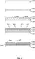
- Figure 4 it is shown the formation of a multi-layer stack comprising a substrate and a dielectric layer formed on the substrate wherein a vent hole for providing a reference pressure is formed in the dielectric layer.
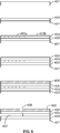
- Figure 5 it is shown the formation of a multi-layer stack comprising a substrate and another layer formed on the substrate wherein a vent hole for providing a reference pressure is formed in the substrate.
- the substrate 301 may comprise or consist of a ceramic material, in particular, an electronically conductive ceramic material.
- a ceramic material in particular, an electronically conductive ceramic material.
- Doped zirconium oxides e.g. doped with yttrium and/or samarium and/or scandium
- doped ceroxides e.g. doped with gadolinium and/or scandium
- Other metals in particular copper, cobalt and/or other transition metals and/or metal alloys may be contained.
- the substrate 301 may be provided in form of a bulk substrate or a multi-layer substrate.
- a dielectric layer 302 is formed on the substrate 301.
- the dielectric layer 302 may be some oxide layer.
- a partial sacrificial layer 303 is formed on the dielectric layer 302.
- the partial sacrificial layer 303 comprises a portion of a sacrificial material 303a (indicated by the dots in Figure 4 ) that will be removed during the further proceedings.
- the partial sacrificial layer 303 comprises a material that will be removed and extends to an edge (on the left-hand side in the configuration shown in Figure 4 ) of the multi-layer stack.
- the sacrificial material may be formed by an appropriate doping or adaptation of depositing parameters.
- forming the partial sacrificial layer 303 comprises forming a layer of a sacrificial material 303a on the dielectric layer 302 and forming adjacent to that layer 303a another layer 303b of a dielectric material on the dielectric layer 302.
- dielectric layer 304 is formed on the partial sacrificial layer 303 (see penultimate row in Figure 4 ). Additionally, layers may be formed on and over the other dielectric layer 304.
- sacrificial material of the partial sacrificial layer 303 is removed (see last row of Figure 4 ).
- removal of the sacrificial material can be achieved by some heating / (short time) annealing procedure 320.
- the sacrificial material may be removed during curing of the (for example, ceramic) substrate 301.
- a vent hole 305 and a channel 306 are formed. It goes without saying that any (and, in particular, more than one) of the dielectric sub-layers can be provided with a sacrificial material.
- one or more channels may be formed by an appropriate selection of the sacrificial material.
- a through passage 307 is formed through overlaying layers (for example, through dielectric layer 304) to the one or more channels 306.
- the through passage 307 connecting to the channel(s) can also be considered being part of a channel that is connected to the vent hole (here vent hole 305).
- a reference pressure can be built up in a cavity of the pressure sensor device wherein a pressure is provided against which the pressure of a test medium can be determined.
- Figure 5 illustrates steps of an alternative manufacturing process.
- a first layer 401 of a substrate is provided (see top row of Figure 5 ).
- the substrate may comprise or consist of a ceramic material, in particular, an electronically conductive ceramic material.
- Doped zirconium oxides e.g. doped with yttrium and/or samarium and/or scandium
- doped ceroxides e.g. doped with gadolinium and/or scandium
- Other metals in particular copper, cobalt and/or other transition metals and/or metal alloys may be contained.
- the substrate is provided in form of a multi-layer substrate.
- a second layer 402 of the substrate is formed on the first layer 401 in the manufacturing stage shown in second row from top of Figure 5 .
- another layer 403 is formed on layer 402 (see third row from top of Figure 5 ).
- Partial sacrificial layer 403 comprises a sacrificial material, for example, formed by doping, indicated by the dots in Figure 5 .
- forming the layer 503 comprises forming a layer of a sacrificial material 403a on the layer 402 and forming adjacent to that layer 403a another layer 403b of a substrate material on the layer 402. The sacrificial material of the substrate will be removed in a later stage of the overall manufacturing process.
- another layer 404 of the substrate is formed on the layer 403 comprising the sacrificial material (see fourth row from top of Figure 5 ).
- a dielectric layer 405 is formed on the layer 404.
- the dielectric layer 405 may be a single-layer or a multi-layer layer.
- the sacrificial material of the partial sacrificial layer 403 is removed (see last row of Figure 5 ).
- removal of the sacrificial material can be achieved by some heating / (short time) annealing procedure.
- the sacrificial material may be removed during curing of the (for example, ceramic) substrate.
- a vent hole 406 and a channel 407 are formed. It goes without saying that any (and, in particular more than one) of the sub-layers of the substrate can be provided with a sacrificial material.
- one or more channels may be formed by an appropriate selection of the sacrificial material.
- a through passage 408 is formed through the dielectric layer 405 and the layer 404 to the one or more channels 407.
- a reference pressure can be built up in a cavity of the pressure sensor device wherein a pressure is provided against which the pressure of a test medium can be determined.
Landscapes
- Physics & Mathematics (AREA)
- General Physics & Mathematics (AREA)
- Chemical & Material Sciences (AREA)
- Engineering & Computer Science (AREA)
- Ceramic Engineering (AREA)
- Analytical Chemistry (AREA)
- Measuring Fluid Pressure (AREA)
- Pressure Sensors (AREA)
- Micromachines (AREA)
Abstract
Description
- The present invention relates to a differential pressure sensor device and, in particular, to a differential pressure sensor device comprising a substrate and another layer comprising channels, and the invention, furthermore, relates to a method of manufacturing such a device.
- Differential pressure sensors measure a difference in pressure between two isolated liquids or gasses. A differential pressure sensor (or transducer) converts a difference in pressure of the liquids or gases to an electrical signal that can be measured to determine the differential pressure value. Generally there are three different transduction mechanisms used to measure pressure such as piezoresistive, piezoelectric, and capacitive. A pressure-sensing device of the sensor is typically manufactured by Micro-Electro-Mechanical System (MEMS) techniques. This technology is used to manufacture commercial semiconductors along with etching and bonding techniques to fabricate very small, inexpensive devices that convert differential pressure to an electrical signal.
- Conventionally, when manufacturing a capacitive or resistive differential pressure sensor a pressure-sensing die is formed from a semiconductor material such as silicon. The die is formed from a silicon wafer by methods such as dicing to produce a silicon structure, which is thinned to create a cavity and define an associated diaphragm. In the case of a piezoresistive elements are formed or placed at the surface of the diaphragm and are configured to exhibit resistance that is proportional to the strain placed on the thinned semiconductor material forming the diaphragm. An electrical circuit connected to the piezoresistive elements creates an electrical signal, based in part on the resistance value of the piezoresistive elements (typically forming a network of Wheatstone bridges). Accordingly, the electrical signal is representative of the pressure of the media under test.
- In a particular class of differential pressure sensors, that are also called gauge type pressure sensors, on one side of the diaphragm (membrane) a pressurized liquid or gas type medium that has to be measured is supplied whereas the other side of the membrane is open to the atmosphere. Thus, the pressure of a test medium is measured against the atmospheric pressure. The connection to the atmosphere is generally called vent(ilation) hole. Since the sensor has a vent hole to allow it to sense atmospheric pressure, the vent hole has to be kept unblocked at all times.
-
Figure 1 shows an example of such adifferential pressure sensor 10 having a vent hole as known in the art. As shown inFigure 1 thesensor 10 has asubstrate 1 and ahousing 2. Surface Mounted Device (SMD)contact pads 3 are provided at the bottom of thesubstrate 1 for contacting a mounting PCB. Another layer (for example, a dielectric layer) 4 on which an electrically conductive pattern can be provided is formed on thesubstrate 1. Over the dielectric layer 4 a microelectromechanical system (MEMS) 5 and an Application Specific Integrated Circuit (ASIC) 6 are formed. The sensing membrane is formed on or by the MEMS top surface. Agel protection 7 is positioned horizontally in thehousing 2. - The pressure of a fluid (liquid or gas) entering from the top (see broad arrow pointing downwards) can be measured against atmospheric pressure built up by an airflow (see thin arrow pointing upwards) through a
vent hole 8 formed through in the bottom surface of the substrate 1 (and positioned between the contact pads 3) and connected to a channel extending from thevent hole 8 through thesubstrate 1 and thedielectric layer 4 to a cavity wherein the atmospheric pressure is built up. However, when thesensor 10 is mounted on a printed circuit board (PCB) for completing the manufacture of an operable device there is risk of clogging the vent hole. Furthermore, there has to be provided for a corresponding through hole in the PCB communicating with the environment and the vent hole of thesensor 10. This through hole formed in the PCB might also be inadvertently blocked, for example, by solder or some conformal coating. - In view of the above, it is an object of the present invention to provide a differential pressure sensor device wherein the atmospheric pressure can be built up and maintained in a more reliable manner as compared to the art.
- The present invention addresses the above-mentioned problem by providing a differential (for example, a gauge) pressure sensor device, comprising a substrate (for example, a multi-layer or bulk ceramic substrate), another layer formed on a main (top) surface of the substrate and a first cavity and a second cavity separated from each other by a membrane. The substrate can be some semiconductor substrate or a high or low temperature co-fired ceramic, for example. Also, a printed circuit board is covered by this term, in general. The other layer can be a dielectric layer and can also be a layer formed of the same material as the substrate. The first cavity is in fluid (liquid or gas) communication with at least one channel that is in fluid communication with a vent hole through which air (or different gas) can enter from an environment of the sensor device (from some reference pressure reservoir or air at atmospheric pressure).
- The at least one channel extends within the other layer or the substrate in a plane that is substantially parallel to the main surface. The at least one channel may also reach a top surface of the substrate and or the other layer. In particular, the substrate can be a multi-layer substrate comprising a plurality of sub-layers and the at least one channel, in this case, may be formed in one of the plurality of sub-layers of the substrate. In particular, the other layer, for example, a dielectric layer, can be a multi-layer layer comprising a plurality of sub-layers and the at least one channel, in this case, may be formed in one of the plurality of sub-layers of the other layer.
- By provision of the vent hole and the channel, for example, atmospheric pressure can be built up and maintained in the first cavity. This allows for measuring the pressure of a test medium supplied from a reservoir through another channel into the second cavity against atmospheric pressure. It should be noted that here and in the following description no restriction to atmospheric pressure is necessary. In fact, the atmospheric pressure can be replaced by any reference pressure supplied by a corresponding reference pressure reservoir.
- The pressure difference is sensed by the membrane. Resistors, for example piezoresistive elements, that may form a network of Wheatstone bridges may be formed on a surface of the membrane. Each of the resistors has a resistance that varies with variations of an applied strain. The differential pressure sensor device may further comprise an MEMS for generating an electrical signal indicative of pressure variations as sensed by the membrane and an ASIC for further processing the electrical signal, wherein the ASIC and the MEMS are formed over the main surface of the substrate.
- Contrary, to the art, a channel connecting the first cavity with the environment (for example, being at atmospheric pressure) via the vent hole is formed in a plane that is parallel to the main surface which implies that the vent hole is not formed in the bottom surface of the substrate (opposite to the main (top) surface). Thereby, the risk of clogging of the vent hole is significantly decreased as compared to the art. In fact, the distance of the vent hole from the mounting surface of the substrate, i.e., the bottom surface, can be arbitrarily chosen along the thickness (vertical) direction of the stack of the substrate and the other layer in a direction perpendicular to the main surface and this distance can be chosen to be sufficiently high in order to prevent clogging by some conformal coating of a mounting PCB to which the substrate may be mounted. No through hole corresponding to the venting hole has to be formed in the mounting PCB at all. Thereby, space is saved since the footprint on the other side of the board is reduced.
- The above-mentioned problem is also solved by a method of manufacturing a differential (gauge) pressure sensor device, wherein the method comprises the following steps:
- forming a substrate (for example made of or comprising a ceramic material or a PCB);
- forming another layer (that, for example, can be formed of a dielectric material or of the same material as the substrate) on a main (top) surface of the substrate;
- forming at least one channel in the other layer or the substrate in a plane parallel to the main surface of the substrate such that the channel forms a vent hole in a minor surface (orientated perpendicular to the main surface) of the other layer or the substrate that is orientated perpendicular to the main surface of the substrate; and
- forming a through passage (for example, in a plane perpendicular to the main surface) through the other layer and connecting to the channel. The through passage also connects to a cavity wherein some reference pressure has to be built up.
- A sensor cell can be formed over the other layer and the substrate. The sensor cell comprises a first cavity for providing for a reference pressure. Thus, the above-mentioned method may comprise forming a first cavity over the other layer by forming a membrane over the other layer, wherein the through passage is formed such that it connects to the first cavity in order to allow built up of a reference pressure (for example, atmospheric pressure) through the vent hole (and the at least one channel). A plurality of resistors, in particular, a plurality of piezoresistive elements, may be formed on a surface of the membrane in order to manufacture a resistive differential pressure sensor device.
- If the vent hole is formed in the other layer, the forming of the other layer may comprise forming a first dielectric sub-layer on the substrate (a single-layer or multi-layer substrate), forming a second dielectric sub-layer partially comprising a sacrificial material or forming a sacrificial layer made of a sacrificial material adjacent to a second dielectric sub-layer on the first dielectric sub-layer and forming a third dielectric sub-layer on the second dielectric sub-layer partially comprising the sacrificial material or on both the sacrificial layer made of the sacrificial material and the adjacent second dielectric sub-layer. In this case, the formation of the channel comprises removing the sacrificial material, for example, by carrying out an anneal process, after formation of the third dielectric sub-layer.
- If the vent hole is formed in the substrate, the forming of the substrate may comprise forming a first substrate sub-layer, forming a second substrate sub-layer partially comprising a sacrificial material or forming a sacrificial layer made of a sacrificial material adjacent to a second substrate sub-layer on the first substrate sub-layer and forming a third substrate sub-layer on the second substrate sub-layer partially comprising the sacrificial material or on both the sacrificial layer made of the sacrificial material and the adjacent second substrate sub-layer. In this case, the formation of the channel comprises removing the sacrificial material, for example, by carrying out an anneal process, after formation of the third substrate sub-layer.
- Alternatively, a channel or a plurality of channels are formed in the substrate or the other layer without the formation of a sacrificial material but rather by laser etching, chemical etching, sawing, etc.
- According to an embodiment an MEMS or another pressure sensing element and an ASIC and a membrane are formed over the other layer and a housing is provided that may partially form the above-mentioned first cavity below (in the direction to the other layer) the membrane and a second cavity above the membrane wherein the second cavity is provided for accommodating a test medium the pressure of which is to be measured against the reference pressure built up in the first cavity. Moreover, a printed circuit board can be bonded to another main (bottom) surface of the substrate that is opposite to the main (top) surface and can be provided with appropriate contact pads.
- Additional features and advantages of the present invention will be described with reference to the drawings. In the description, reference is made to the accompanying figures that are meant to illustrate preferred embodiments of the invention. It is understood that such embodiments do not represent the full scope of the invention.
-
Figure 1 schematically illustrates a differential pressure sensor device according to an example of the prior art. -
Figure 2 illustrates a differential pressure sensor device with one or more channels formed in another layer according to an embodiment of the present invention. -
Figure 3 illustrates a differential pressure sensor device with one or more channels formed in a substrate according to another embodiment of the present invention. -
Figure 4 shows steps of manufacturing of a differential pressure sensor device wherein a vent hole is formed in another layer. -
Figure 5 shows steps of manufacturing of a differential pressure sensor device wherein a vent hole is formed in a substrate. - The present invention provides a differential pressure sensor device, for example, a differential pressure sensor device wherein pressure of a test medium is measured against some reference pressure, for example, against atmospheric pressure (gauge pressure sensor device). An embodiment of the inventive differential
pressure sensor device 100 is illustrated inFigure 2 . The differentialpressure sensor device 100 comprises asubstrate 110 and ahousing 102. - The
substrate 110 may be made of a ceramic material, in particular, an electronically conductive ceramic material. Doped zirconium oxides (e.g. doped with yttrium and/or samarium and/or scandium) and/or doped ceroxides (e.g. doped with gadolinium and/or scandium) are examples for the ceramic material. Other metals, in particular copper, cobalt and/or other transition metals and/or metal alloys may be contained. - The
housing 102 may be made of materials such as silicon or other semiconductor materials, glass, metal, plastic, ceramic as well as other suitable materials. A seal may be formed at the upper surface of thehousing 102 and the underside ofsubstrate 110 using an O-ring seal, for example. Thehousing 102 may be attached to thesubstrate 110 via some adhesive, solder or glass frit. - Another
layer 104 is formed on a top main surface (orientated in the horizontal direction inFigure 2 ) of thesubstrate 110. Theother layer 104 may, for example, be made of or comprise a dielectric, for example, some oxide material. Contactpads 103 for electrically contacting a mounting PCB are formed on a main bottom surface of thesubstrate 110. - An
MEMS 105 and anASIC 106 are provided in thehousing 102 above the top main surface of thesubstrate 110 and thedielectric layer 103. A sensing membrane is formed on or by a top surface of the MEMS. Agel protection 107 is, furthermore, provided in thehousing 102 and separates two cavities from each other. For example, the flexible membrane that contacts the measured media may comprise stainless steel. The flexible membrane is configured to flex when the resulting net pressure difference of the media exerts a force to the surface of the flexible membrane. Resistors R, for example piezoresistive elements, that may form a network of Wheatstone bridges may be formed on a surface of the membrane. - By applying a first pressure to a first surface of the membrane, while simultaneously applying a second pressure to a second surface of the membrane opposite the first surface the membrane will experience a force which is representative for the net pressure difference between the pressures applied to the first and second surfaces. The piezoresistive elements will exhibit a resistance representative of this net pressure difference applied to the membrane. The
MEMS 105 outputs electrical signals indicative of pressure variations sensed by the (resistors of the) membrane to theMEMS ASIC 106. TheASIC 106 may process the electrical signals for analog to digital conversion and/or amplification, noise filtering, etc., as desired. Thehousing 102 may include other pressure sensor components, such as, oil-filled isolated volumes which prevent harsh media whose pressure is being measured from coming into contact with the sensitive membrane and theASIC 106 and theMEMS 105. Protection can also by provided by some appropriate coating. - A
vent hole 108 is formed in theother layer 104 and connected by a channel or a plurality ofchannels 109 that extends horizontally inFigure 2 and connect to aninlet 120. The channel(s) 109 is (are) formed within thedielectric layer 104 in a plane that is substantially parallel to the main top surface of thesubstrate 110 on which thedielectric layer 104 is formed. The channel(s) 9 is (are) in fluid communication with thevent hole 108 and theinlet 120. Thereby, an atmospheric pressure can be built up (see arrow inFigure 2 ) and maintained in the lower one of the cavities partially built by the membrane , if thevent hole 108 represents an inlet to natural environment. Alternatively, any reservoir providing any reference pressure different from atmospheric pressure can be connected to thevent hole 108. -
Figure 3 illustrates an alternative embodiment of the inventive differentialpressure sensor device 200. The differentialpressure sensor device 200 comprises amulti-layer substrate 210 including at least threesub-layers housing 102. Another layer 104 (for example, a dielectric layer) is formed on themulti-layer substrate 210. Thehousing 202 houses anMEMS 205, anASIC 206 and agel protection 207. Materials of the various components can be chosen similar to the ones mentioned above in the context of the description of the embodiment shown inFigure 2 . Resistors R, for example piezoresistive elements, that may form a network of Wheatstone bridges may be formed on a surface of the membrane M formed on or by a top surface of theMEMS 205. The membrane M separates a first cavity C1 from a second cavity C2. A test (measuring) medium may be introduced in the second cavity C2 and the pressure of the test medium may be measured against the pressure of a reference medium introduced into the first cavity C1. The reference medium may be air with atmospheric pressure. - Different from the embodiment shown in
Figure 2 one ormore channels 209 are formed in one or more of thesub-layers substrate 210 in a plane that is parallel to a top main surface of thesubstrate 210 and connected to aninlet 220. Moreover, the channel(s) 209 is (are) connected to avent hole 208 that is formed in a minor surface (orientated perpendicular to the main surface) of thesubstrate 210. If thevent hole 208 is directed to a natural environment atmospheric pressure can be built up and maintained in the first cavity C1. - In the above-described embodiments a vent hole and one or more channels connected to the vent hole and extending parallel to the top main surface of the substrate are provided in a manner that avoid or at least reduced the risk of clogging of the vent hole. In the following, exemplary procedures for manufacturing the a differential pressure sensor device, for example, one of the differential
pressure sensor devices Figure 2 andFigure 3 , respectively, are described with reference toFigures 4 and5 . - The differential pressure sensor device according to embodiments of the present invention comprises a substrate and another layer formed on the substrate. Active components of the differential pressure sensor device are formed over the substrate and the dielectric layer. In the following description, it is assumed that the other layer is a dielectric layer for exemplary purposes. In
Figure 4 it is shown the formation of a multi-layer stack comprising a substrate and a dielectric layer formed on the substrate wherein a vent hole for providing a reference pressure is formed in the dielectric layer. InFigure 5 it is shown the formation of a multi-layer stack comprising a substrate and another layer formed on the substrate wherein a vent hole for providing a reference pressure is formed in the substrate. - In the embodiment illustrated in
Figure 4 asubstrate 301 is provided (see top row ofFigure 4 ). Thesubstrate 301 may comprise or consist of a ceramic material, in particular, an electronically conductive ceramic material. Doped zirconium oxides (e.g. doped with yttrium and/or samarium and/or scandium) and/or doped ceroxides (e.g. doped with gadolinium and/or scandium) are examples for the ceramic material. Other metals, in particular copper, cobalt and/or other transition metals and/or metal alloys may be contained. Thesubstrate 301 may be provided in form of a bulk substrate or a multi-layer substrate. - In the manufacturing step shown in the second row from top in
Figure 4 adielectric layer 302 is formed on thesubstrate 301. Thedielectric layer 302 may be some oxide layer. As shown in the third row from top inFigure 4 a partialsacrificial layer 303 is formed on thedielectric layer 302. The partialsacrificial layer 303 comprises a portion of asacrificial material 303a (indicated by the dots inFigure 4 ) that will be removed during the further proceedings. In particular, the partialsacrificial layer 303 comprises a material that will be removed and extends to an edge (on the left-hand side in the configuration shown inFigure 4 ) of the multi-layer stack. The sacrificial material may be formed by an appropriate doping or adaptation of depositing parameters. According to an embodiment, forming the partialsacrificial layer 303 comprises forming a layer of asacrificial material 303a on thedielectric layer 302 and forming adjacent to thatlayer 303a anotherlayer 303b of a dielectric material on thedielectric layer 302. - Subsequently, another
dielectric layer 304 is formed on the partial sacrificial layer 303 (see penultimate row inFigure 4 ). Additionally, layers may be formed on and over the otherdielectric layer 304. - At some stage of the overall manufacturing process, sacrificial material of the partial
sacrificial layer 303 is removed (see last row ofFigure 4 ). For example, removal of the sacrificial material can be achieved by some heating / (short time)annealing procedure 320. The sacrificial material may be removed during curing of the (for example, ceramic)substrate 301. By removal of the sacrificial material of the partialsacrificial layer 303 avent hole 305 and achannel 306 are formed. It goes without saying that any (and, in particular, more than one) of the dielectric sub-layers can be provided with a sacrificial material. - It is noted that one or more channels may be formed by an appropriate selection of the sacrificial material. In a later stage of the overall manufacturing process a through
passage 307 is formed through overlaying layers (for example, through dielectric layer 304) to the one ormore channels 306. Regarding the used terminology here and in the following, the throughpassage 307 connecting to the channel(s) can also be considered being part of a channel that is connected to the vent hole (here vent hole 305). By means of the through passage, the channel(s) 306 and the vent hole 305 a reference pressure can be built up in a cavity of the pressure sensor device wherein a pressure is provided against which the pressure of a test medium can be determined. - Subsequently, other components of the differential pressure sensor device are formed over the dielectric layer 304 (see
Figure 2 ). -
Figure 5 illustrates steps of an alternative manufacturing process. Afirst layer 401 of a substrate is provided (see top row ofFigure 5 ). The substrate may comprise or consist of a ceramic material, in particular, an electronically conductive ceramic material. Doped zirconium oxides (e.g. doped with yttrium and/or samarium and/or scandium) and/or doped ceroxides (e.g. doped with gadolinium and/or scandium) are examples for the ceramic material. Other metals, in particular copper, cobalt and/or other transition metals and/or metal alloys may be contained. The substrate is provided in form of a multi-layer substrate. - A
second layer 402 of the substrate is formed on thefirst layer 401 in the manufacturing stage shown in second row from top ofFigure 5 . Subsequently, anotherlayer 403 is formed on layer 402 (see third row from top ofFigure 5 ). Partialsacrificial layer 403 comprises a sacrificial material, for example, formed by doping, indicated by the dots inFigure 5 . According to an embodiment, forming the layer 503 comprises forming a layer of asacrificial material 403a on thelayer 402 and forming adjacent to thatlayer 403a anotherlayer 403b of a substrate material on thelayer 402. The sacrificial material of the substrate will be removed in a later stage of the overall manufacturing process. - In a further developed manufacturing stage, another
layer 404 of the substrate is formed on thelayer 403 comprising the sacrificial material (see fourth row from top ofFigure 5 ). Subsequently, adielectric layer 405 is formed on thelayer 404. Thedielectric layer 405 may be a single-layer or a multi-layer layer. - At some stage of the overall manufacturing process, the sacrificial material of the partial
sacrificial layer 403 is removed (see last row ofFigure 5 ). For example, removal of the sacrificial material can be achieved by some heating / (short time) annealing procedure. The sacrificial material may be removed during curing of the (for example, ceramic) substrate. By removal of the sacrificial material of the partialsacrificial layer 403 a vent hole 406 and achannel 407 are formed. It goes without saying that any (and, in particular more than one) of the sub-layers of the substrate can be provided with a sacrificial material. - It is noted that one or more channels may be formed by an appropriate selection of the sacrificial material. In a later stage of the overall manufacturing process, a through
passage 408 is formed through thedielectric layer 405 and thelayer 404 to the one ormore channels 407. By means of the throughpassage 408, the channel(s) 407 and the vent hole 406 a reference pressure can be built up in a cavity of the pressure sensor device wherein a pressure is provided against which the pressure of a test medium can be determined. - While embodiments of the present disclosure have been described as utilizing, for example, piezoresistive elements to detect strain of a pressure-sensing diaphragm, it should be understood that any suitable type of pressure-sensing technology may be implemented without departing from the scope of the present disclosure. A sensing element is not necessarily provided by means of an MEMS. Other examples cover a ceramic membrane. For example, pressure sensor devices disclosed herein may implement capacitive, electromagnetic, piezoelectric, optical or thermal pressure-sensing techniques, as will be understood by a person skilled in the art.
- All previously discussed embodiments are not intended as limitations but serve as examples illustrating features and advantages of the invention. It is to be understood that some or all of the above-described features can also be combined in different ways.
Claims (15)
- A differential pressure sensor device (100, 200), comprising
a substrate (110, 210);
another layer (104, 204, 405) formed on a main surface of the substrate (110, 210);
a first cavity (C1) and a second cavity (C2) separated from each other by a membrane (M);
wherein the first cavity (C1) is in fluid communication with a channel (109, 209, 306, 407) that is in fluid communication with a vent hole (108, 208, 305, 406);
characterized in that
the channel (109, 209, 306, 407) extends within the other layer or the substrate (110, 210) in a plane that is substantially parallel to the main surface of the substrate (110, 210). - A differential pressure sensor device (100, 200) according to claim 1, further comprising another channel in fluid communication with the second cavity and a reservoir of a test medium.
- A differential pressure sensor device (100, 200) according to claim 1 or 2, further comprising a printed circuit board bonded to another main surface of the substrate (110, 210) that is opposite to the main surface of the substrate (110, 210).
- A differential pressure sensor device (100, 200) according to one of the preceding claims, further comprising an Application Specific Integrated Circuit, ASIC, (106, 206) and/or a microelectromechanical system, MEMS, (105, 205) or another pressure sensing element, wherein the MEMS is configured to output electrical signals indicative of pressure variations sensed by the membrane (M) to the ASIC and the ASIC is configured to process the electrical signals by amplification and/or analog-to-digital conversion and/or noise filtering.
- A differential pressure sensor device (100, 200) according to one of the preceding claims, wherein a plurality of resistors, in particular, a plurality of piezoresistive elements, are formed on a surface of the membrane (M).
- A differential pressure sensor device (100, 200) according to one of the preceding claims, wherein the vent hole (108, 208, 305, 406) is in fluid communication with an environment of the differential pressure sensor device (100, 200) such that an atmospheric pressure can be built up in the first cavity (C1).
- A differential pressure sensor device (200) according to one of the preceding claims, wherein the substrate (210) is a multi-layer substrate comprising a plurality of sub-layers and wherein the channel (209, 407) is formed in one of the plurality of sub-layers.
- A differential pressure sensor device (100, 200) according to one of the claims 1 to 6, wherein the other layer (104) comprises a plurality of sub-layers and wherein the channel (109, 306) is formed in one of the plurality of sub-layers.
- A method of manufacturing a differential pressure sensor device (100, 200), comprising the steps of
forming a substrate (110, 210);
forming another layer (104, 204, 405) on a main surface of the substrate (110, 210);
forming a channel (109, 209, 306, 407) in the other layer (104, 204, 405) or the substrate (110, 210) in a plane parallel to the main surface of the substrate (110, 210) such that the channel (109, 209, 306, 407) forms a vent hole (108, 208, 305, 406) in a minor surface of the other layer (104, 204, 405) or the substrate (110, 210) that is orientated perpendicular to the main surface of the substrate (110, 210); and
forming a through passage through the other layer (104, 204, 405) and connecting to the channel (109, 209, 306, 407). - A method according to claim 9, further comprising forming a first cavity (C1) over the other layer (104, 204, 405) by forming a membrane (M) over the other layer (104, 204, 405) and wherein the through passage is formed such that it connects to the first cavity (C1).
- A method according to claim 9 or 10, wherein
the channel (109, 306) is formed in the other layer (104);
the vent hole (108, 305) is formed in the minor surface of the other layer (104, 204); and
forming the other layer (104) comprises forming a first other sub-layer (302) on the substrate (110, 301), forming either a second other sub-layer (303) partially comprising a sacrificial material or a sacrificial layer comprising a sacrificial material adjacent to a second other sub-layer over the first other sub-layer (302) and forming a third other sub-layer (304) on the second other sub-layer (303) partially comprising the sacrificial material or on both the sacrificial layer comprising the sacrificial material and the adjacent second other sub-layer; and
forming the channel (109, 306) in the other layer (104) comprises removing the sacrificial material after formation of the third other sub-layer (304). - A method according to one of the claims 9 or 10, wherein
the channel (209, 407) is formed in the substrate (110, 210);
the vent hole (208, 406) is formed in the minor surface of the substrate (210); and
forming the substrate (210) comprises forming a first substrate sub-layer (401), forming either a second substrate sub-layer (403) partially comprising a sacrificial material or a sacrificial layer comprising a sacrificial material adjacent to a second substrate sub-layer over the first substrate sub-layer (401) and forming a third substrate sub-layer (404) on the second substrate sub-layer (403) partially comprising the sacrificial material or on both the sacrificial layer comprising the sacrificial material and the adjacent second substrate sub-layer; and
forming the channel (209, 407) in the substrate (210) comprises removing the sacrificial material after formation of the third substrate sub-layer (404). - A method according to one of the claims 9 to 12, further comprising
forming contact pads at another main surface of the substrate (110, 210) that is opposite to the main surface of the substrate (110, 210);
bonding a printed circuit board to other mains surface; and
forming an Application Specific Integrated Circuit, ASIC, and a microelectromechanical system, MEMS, over the other layer (104, 204, 405). - A method according to one of the claims 9 to 13, further comprising forming a plurality of resistors, in particular, a plurality of piezoresistive elements, on a surface of the membrane (M).
- A differential pressure sensor device (100, 200) obtainable by a method according to one of the claims 9 to 14.
Priority Applications (6)
| Application Number | Priority Date | Filing Date | Title |
|---|---|---|---|
| EP18206582.1A EP3654005B1 (en) | 2018-11-15 | 2018-11-15 | Differential pressure sensor device |
| US16/677,548 US11231338B2 (en) | 2018-11-15 | 2019-11-07 | Differential pressure sensor device having channel in fluid communication with a vent hole |
| JP2019203660A JP2020085902A (en) | 2018-11-15 | 2019-11-11 | Differential sensor device |
| KR1020190146018A KR102679631B1 (en) | 2018-11-15 | 2019-11-14 | Differential Pressure Sensor Device |
| CN201911111101.5A CN111189574A (en) | 2018-11-15 | 2019-11-14 | Differential pressure sensor device |
| JP2024022660A JP2024059734A (en) | 2018-11-15 | 2024-02-19 | Differential Pressure Sensor Device |
Applications Claiming Priority (1)
| Application Number | Priority Date | Filing Date | Title |
|---|---|---|---|
| EP18206582.1A EP3654005B1 (en) | 2018-11-15 | 2018-11-15 | Differential pressure sensor device |
Publications (2)
| Publication Number | Publication Date |
|---|---|
| EP3654005A1 true EP3654005A1 (en) | 2020-05-20 |
| EP3654005B1 EP3654005B1 (en) | 2022-05-11 |
Family
ID=64331829
Family Applications (1)
| Application Number | Title | Priority Date | Filing Date |
|---|---|---|---|
| EP18206582.1A Active EP3654005B1 (en) | 2018-11-15 | 2018-11-15 | Differential pressure sensor device |
Country Status (5)
| Country | Link |
|---|---|
| US (1) | US11231338B2 (en) |
| EP (1) | EP3654005B1 (en) |
| JP (2) | JP2020085902A (en) |
| KR (1) | KR102679631B1 (en) |
| CN (1) | CN111189574A (en) |
Cited By (1)
| Publication number | Priority date | Publication date | Assignee | Title |
|---|---|---|---|---|
| CN118359167A (en) * | 2024-06-19 | 2024-07-19 | 苏州敏芯微电子技术股份有限公司 | Method for manufacturing micro differential pressure chip and micro differential pressure chip |
Families Citing this family (3)
| Publication number | Priority date | Publication date | Assignee | Title |
|---|---|---|---|---|
| CN110082027A (en) * | 2019-04-09 | 2019-08-02 | 苏州敏芯微电子技术股份有限公司 | Differential pressure pick-up encapsulating structure and electronic equipment |
| CN112857655B (en) * | 2021-03-30 | 2025-04-08 | 明晶芯晟(成都)科技有限责任公司 | Array pressure measurement device based on ceramic substrate |
| CN113654713A (en) * | 2021-07-15 | 2021-11-16 | 重庆市伟岸测器制造股份有限公司 | a pressure balancing system |
Citations (2)
| Publication number | Priority date | Publication date | Assignee | Title |
|---|---|---|---|---|
| US20070227254A1 (en) * | 2004-06-03 | 2007-10-04 | Nagano Keiki Co., Ltd. | Pressure Sensor Module and Pressure Detecting Device |
| US20100230766A1 (en) * | 2009-03-12 | 2010-09-16 | Infineon Technologies Ag | Sensor device and method |
Family Cites Families (25)
| Publication number | Priority date | Publication date | Assignee | Title |
|---|---|---|---|---|
| JP2823889B2 (en) * | 1989-08-04 | 1998-11-11 | 三菱電機株式会社 | Pressure detector |
| US5125275A (en) * | 1991-06-19 | 1992-06-30 | Honeywell Inc. | Pressure sensor package |
| JPH0719979A (en) * | 1993-06-29 | 1995-01-20 | Omron Corp | Pressure sensor chip and pressure sensor |
| JP3042344B2 (en) * | 1995-01-27 | 2000-05-15 | 松下電工株式会社 | Semiconductor pressure sensor |
| JPH08247873A (en) * | 1995-03-13 | 1996-09-27 | Tokai Rika Co Ltd | Pressure sensor |
| EP0890998A1 (en) * | 1997-07-07 | 1999-01-13 | STMicroelectronics S.r.l. | Manufacturing method and integrated piezoresistive pressure sensor having a diaphragm of polycristalline semiconductor material |
| JPH11248578A (en) * | 1998-03-05 | 1999-09-17 | Omron Corp | Capacitive pressure sensor and package structure thereof |
| WO2001046665A1 (en) * | 1999-12-20 | 2001-06-28 | The Foxboro Company | Multivariate semiconductor pressure sensor with passageway |
| CN101445945A (en) * | 2002-05-07 | 2009-06-03 | 微制造公司 | Multistep release method for electrochemically fabricated structures |
| JP2005091166A (en) * | 2003-09-17 | 2005-04-07 | Matsushita Electric Works Ltd | Semiconductor pressure sensor |
| CN101069078B (en) * | 2004-12-08 | 2011-04-06 | Abb专利有限公司 | Differential pressure transducer unit |
| DE112004002994A5 (en) * | 2004-12-08 | 2007-10-31 | Abb Patent Gmbh | Method of manufacturing a transmitter |
| US7080559B1 (en) * | 2005-03-08 | 2006-07-25 | Sensfab Pte Ltd | Transducer |
| JP2006322783A (en) * | 2005-05-18 | 2006-11-30 | Dainippon Screen Mfg Co Ltd | Pressure sensor and substrate processing apparatus |
| JP2010133900A (en) * | 2008-12-08 | 2010-06-17 | Yamatake Corp | Electronic device, method for manufacturing the same, and flowmeter |
| US8359927B2 (en) * | 2009-08-12 | 2013-01-29 | Freescale Semiconductor, Inc. | Molded differential PRT pressure sensor |
| JP5419923B2 (en) * | 2011-05-09 | 2014-02-19 | 三菱電機株式会社 | Sensor element |
| US8921952B2 (en) * | 2013-01-29 | 2014-12-30 | Freescale Semiconductor Inc. | Microelectromechanical system devices having crack resistant membrane structures and methods for the fabrication thereof |
| CH708708A1 (en) * | 2013-10-03 | 2015-04-15 | Kistler Holding Ag | Measuring element for measuring a pressure and pressure measuring sensor. |
| CN104655333B (en) * | 2013-11-21 | 2017-04-05 | 中芯国际集成电路制造(上海)有限公司 | A kind of pressure transducer and preparation method thereof |
| JP6292932B2 (en) * | 2014-03-13 | 2018-03-14 | セイコーインスツル株式会社 | Pressure sensor |
| DE102014012918B4 (en) * | 2014-09-05 | 2019-01-03 | Heinz Plöchinger | Dual-capacity pressure gauge with a small measuring volume |
| EP3368874A4 (en) * | 2015-10-28 | 2019-06-05 | Hewlett-Packard Development Company, L.P. | Relative pressure sensor |
| JP6373318B2 (en) * | 2016-05-17 | 2018-08-15 | エーエーシー テクノロジーズ ピーティーイー リミテッドAac Technologies Pte.Ltd. | pressure sensor |
| US10203255B2 (en) * | 2016-08-25 | 2019-02-12 | Measurement Specialties, Inc. | Differential pressure sensor incorporating common mode error compensation |
-
2018
- 2018-11-15 EP EP18206582.1A patent/EP3654005B1/en active Active
-
2019
- 2019-11-07 US US16/677,548 patent/US11231338B2/en active Active
- 2019-11-11 JP JP2019203660A patent/JP2020085902A/en active Pending
- 2019-11-14 CN CN201911111101.5A patent/CN111189574A/en active Pending
- 2019-11-14 KR KR1020190146018A patent/KR102679631B1/en active Active
-
2024
- 2024-02-19 JP JP2024022660A patent/JP2024059734A/en active Pending
Patent Citations (2)
| Publication number | Priority date | Publication date | Assignee | Title |
|---|---|---|---|---|
| US20070227254A1 (en) * | 2004-06-03 | 2007-10-04 | Nagano Keiki Co., Ltd. | Pressure Sensor Module and Pressure Detecting Device |
| US20100230766A1 (en) * | 2009-03-12 | 2010-09-16 | Infineon Technologies Ag | Sensor device and method |
Cited By (1)
| Publication number | Priority date | Publication date | Assignee | Title |
|---|---|---|---|---|
| CN118359167A (en) * | 2024-06-19 | 2024-07-19 | 苏州敏芯微电子技术股份有限公司 | Method for manufacturing micro differential pressure chip and micro differential pressure chip |
Also Published As
| Publication number | Publication date |
|---|---|
| US20200158587A1 (en) | 2020-05-21 |
| KR20200057649A (en) | 2020-05-26 |
| KR102679631B1 (en) | 2024-07-01 |
| US11231338B2 (en) | 2022-01-25 |
| CN111189574A (en) | 2020-05-22 |
| JP2020085902A (en) | 2020-06-04 |
| JP2024059734A (en) | 2024-05-01 |
| EP3654005B1 (en) | 2022-05-11 |
Similar Documents
| Publication | Publication Date | Title |
|---|---|---|
| KR101355838B1 (en) | Pressure sensor with silicon frit bonded cap | |
| US11231338B2 (en) | Differential pressure sensor device having channel in fluid communication with a vent hole | |
| JP4726481B2 (en) | Barometric pressure sensor | |
| EP2568270B1 (en) | Packaged sensor with multiple sensors elements | |
| US5285690A (en) | Pressure sensor having a laminated substrate | |
| US9470593B2 (en) | Media isolated pressure sensor | |
| KR101953454B1 (en) | Pressure sensor chip | |
| CN107782485B (en) | Differential pressure sensor integrated with common mode error compensation | |
| US8393223B2 (en) | Pressure sensor with resistance strain gages | |
| EP3748324B1 (en) | Pressure sensor assemblies with protective pressure feature | |
| US11079298B2 (en) | MEMS pressure sensor with multiple sensitivity and small dimensions | |
| JP2005121631A (en) | Flowmeter with composite technology | |
| US10048139B2 (en) | Pressure transducer structures suitable for curved surfaces | |
| EP3515858B1 (en) | Method of manufacturing a sensor using anodic bonding | |
| JP5981571B2 (en) | Micromechanical measuring element and manufacturing method of micromechanical measuring element | |
| JP4739164B2 (en) | Semiconductor strain sensitive sensor for measuring intake air pressure of vehicle engine | |
| JP6218330B2 (en) | Pressure sensor and manufacturing method thereof | |
| CN119873724A (en) | Pressure sensor with improved suppression of undesired stimulus | |
| CN114441069A (en) | Piezoresistive pressure sensor suitable for explosion field and preparation method thereof |
Legal Events
| Date | Code | Title | Description |
|---|---|---|---|
| PUAI | Public reference made under article 153(3) epc to a published international application that has entered the european phase |
Free format text: ORIGINAL CODE: 0009012 |
|
| STAA | Information on the status of an ep patent application or granted ep patent |
Free format text: STATUS: THE APPLICATION HAS BEEN PUBLISHED |
|
| AK | Designated contracting states |
Kind code of ref document: A1 Designated state(s): AL AT BE BG CH CY CZ DE DK EE ES FI FR GB GR HR HU IE IS IT LI LT LU LV MC MK MT NL NO PL PT RO RS SE SI SK SM TR |
|
| AX | Request for extension of the european patent |
Extension state: BA ME |
|
| STAA | Information on the status of an ep patent application or granted ep patent |
Free format text: STATUS: REQUEST FOR EXAMINATION WAS MADE |
|
| 17P | Request for examination filed |
Effective date: 20200608 |
|
| RBV | Designated contracting states (corrected) |
Designated state(s): AL AT BE BG CH CY CZ DE DK EE ES FI FR GB GR HR HU IE IS IT LI LT LU LV MC MK MT NL NO PL PT RO RS SE SI SK SM TR |
|
| STAA | Information on the status of an ep patent application or granted ep patent |
Free format text: STATUS: EXAMINATION IS IN PROGRESS |
|
| 17Q | First examination report despatched |
Effective date: 20210217 |
|
| GRAP | Despatch of communication of intention to grant a patent |
Free format text: ORIGINAL CODE: EPIDOSNIGR1 |
|
| STAA | Information on the status of an ep patent application or granted ep patent |
Free format text: STATUS: GRANT OF PATENT IS INTENDED |
|
| INTG | Intention to grant announced |
Effective date: 20211215 |
|
| RAP3 | Party data changed (applicant data changed or rights of an application transferred) |
Owner name: TE CONNECTIVITY SOLUTIONS GMBH |
|
| GRAS | Grant fee paid |
Free format text: ORIGINAL CODE: EPIDOSNIGR3 |
|
| GRAA | (expected) grant |
Free format text: ORIGINAL CODE: 0009210 |
|
| STAA | Information on the status of an ep patent application or granted ep patent |
Free format text: STATUS: THE PATENT HAS BEEN GRANTED |
|
| AK | Designated contracting states |
Kind code of ref document: B1 Designated state(s): AL AT BE BG CH CY CZ DE DK EE ES FI FR GB GR HR HU IE IS IT LI LT LU LV MC MK MT NL NO PL PT RO RS SE SI SK SM TR |
|
| REG | Reference to a national code |
Ref country code: GB Ref legal event code: FG4D |
|
| REG | Reference to a national code |
Ref country code: CH Ref legal event code: EP |
|
| REG | Reference to a national code |
Ref country code: AT Ref legal event code: REF Ref document number: 1491804 Country of ref document: AT Kind code of ref document: T Effective date: 20220515 |
|
| REG | Reference to a national code |
Ref country code: DE Ref legal event code: R096 Ref document number: 602018035335 Country of ref document: DE |
|
| REG | Reference to a national code |
Ref country code: IE Ref legal event code: FG4D |
|
| REG | Reference to a national code |
Ref country code: LT Ref legal event code: MG9D |
|
| REG | Reference to a national code |
Ref country code: NL Ref legal event code: MP Effective date: 20220511 |
|
| REG | Reference to a national code |
Ref country code: AT Ref legal event code: MK05 Ref document number: 1491804 Country of ref document: AT Kind code of ref document: T Effective date: 20220511 |
|
| PG25 | Lapsed in a contracting state [announced via postgrant information from national office to epo] |
Ref country code: SE Free format text: LAPSE BECAUSE OF FAILURE TO SUBMIT A TRANSLATION OF THE DESCRIPTION OR TO PAY THE FEE WITHIN THE PRESCRIBED TIME-LIMIT Effective date: 20220511 Ref country code: PT Free format text: LAPSE BECAUSE OF FAILURE TO SUBMIT A TRANSLATION OF THE DESCRIPTION OR TO PAY THE FEE WITHIN THE PRESCRIBED TIME-LIMIT Effective date: 20220912 Ref country code: NO Free format text: LAPSE BECAUSE OF FAILURE TO SUBMIT A TRANSLATION OF THE DESCRIPTION OR TO PAY THE FEE WITHIN THE PRESCRIBED TIME-LIMIT Effective date: 20220811 Ref country code: NL Free format text: LAPSE BECAUSE OF FAILURE TO SUBMIT A TRANSLATION OF THE DESCRIPTION OR TO PAY THE FEE WITHIN THE PRESCRIBED TIME-LIMIT Effective date: 20220511 Ref country code: LT Free format text: LAPSE BECAUSE OF FAILURE TO SUBMIT A TRANSLATION OF THE DESCRIPTION OR TO PAY THE FEE WITHIN THE PRESCRIBED TIME-LIMIT Effective date: 20220511 Ref country code: HR Free format text: LAPSE BECAUSE OF FAILURE TO SUBMIT A TRANSLATION OF THE DESCRIPTION OR TO PAY THE FEE WITHIN THE PRESCRIBED TIME-LIMIT Effective date: 20220511 Ref country code: GR Free format text: LAPSE BECAUSE OF FAILURE TO SUBMIT A TRANSLATION OF THE DESCRIPTION OR TO PAY THE FEE WITHIN THE PRESCRIBED TIME-LIMIT Effective date: 20220812 Ref country code: FI Free format text: LAPSE BECAUSE OF FAILURE TO SUBMIT A TRANSLATION OF THE DESCRIPTION OR TO PAY THE FEE WITHIN THE PRESCRIBED TIME-LIMIT Effective date: 20220511 Ref country code: ES Free format text: LAPSE BECAUSE OF FAILURE TO SUBMIT A TRANSLATION OF THE DESCRIPTION OR TO PAY THE FEE WITHIN THE PRESCRIBED TIME-LIMIT Effective date: 20220511 Ref country code: BG Free format text: LAPSE BECAUSE OF FAILURE TO SUBMIT A TRANSLATION OF THE DESCRIPTION OR TO PAY THE FEE WITHIN THE PRESCRIBED TIME-LIMIT Effective date: 20220811 Ref country code: AT Free format text: LAPSE BECAUSE OF FAILURE TO SUBMIT A TRANSLATION OF THE DESCRIPTION OR TO PAY THE FEE WITHIN THE PRESCRIBED TIME-LIMIT Effective date: 20220511 |
|
| PG25 | Lapsed in a contracting state [announced via postgrant information from national office to epo] |
Ref country code: RS Free format text: LAPSE BECAUSE OF FAILURE TO SUBMIT A TRANSLATION OF THE DESCRIPTION OR TO PAY THE FEE WITHIN THE PRESCRIBED TIME-LIMIT Effective date: 20220511 Ref country code: PL Free format text: LAPSE BECAUSE OF FAILURE TO SUBMIT A TRANSLATION OF THE DESCRIPTION OR TO PAY THE FEE WITHIN THE PRESCRIBED TIME-LIMIT Effective date: 20220511 Ref country code: LV Free format text: LAPSE BECAUSE OF FAILURE TO SUBMIT A TRANSLATION OF THE DESCRIPTION OR TO PAY THE FEE WITHIN THE PRESCRIBED TIME-LIMIT Effective date: 20220511 Ref country code: IS Free format text: LAPSE BECAUSE OF FAILURE TO SUBMIT A TRANSLATION OF THE DESCRIPTION OR TO PAY THE FEE WITHIN THE PRESCRIBED TIME-LIMIT Effective date: 20220911 |
|
| PG25 | Lapsed in a contracting state [announced via postgrant information from national office to epo] |
Ref country code: SM Free format text: LAPSE BECAUSE OF FAILURE TO SUBMIT A TRANSLATION OF THE DESCRIPTION OR TO PAY THE FEE WITHIN THE PRESCRIBED TIME-LIMIT Effective date: 20220511 Ref country code: SK Free format text: LAPSE BECAUSE OF FAILURE TO SUBMIT A TRANSLATION OF THE DESCRIPTION OR TO PAY THE FEE WITHIN THE PRESCRIBED TIME-LIMIT Effective date: 20220511 Ref country code: RO Free format text: LAPSE BECAUSE OF FAILURE TO SUBMIT A TRANSLATION OF THE DESCRIPTION OR TO PAY THE FEE WITHIN THE PRESCRIBED TIME-LIMIT Effective date: 20220511 Ref country code: EE Free format text: LAPSE BECAUSE OF FAILURE TO SUBMIT A TRANSLATION OF THE DESCRIPTION OR TO PAY THE FEE WITHIN THE PRESCRIBED TIME-LIMIT Effective date: 20220511 Ref country code: DK Free format text: LAPSE BECAUSE OF FAILURE TO SUBMIT A TRANSLATION OF THE DESCRIPTION OR TO PAY THE FEE WITHIN THE PRESCRIBED TIME-LIMIT Effective date: 20220511 Ref country code: CZ Free format text: LAPSE BECAUSE OF FAILURE TO SUBMIT A TRANSLATION OF THE DESCRIPTION OR TO PAY THE FEE WITHIN THE PRESCRIBED TIME-LIMIT Effective date: 20220511 |
|
| REG | Reference to a national code |
Ref country code: DE Ref legal event code: R097 Ref document number: 602018035335 Country of ref document: DE |
|
| PLBE | No opposition filed within time limit |
Free format text: ORIGINAL CODE: 0009261 |
|
| STAA | Information on the status of an ep patent application or granted ep patent |
Free format text: STATUS: NO OPPOSITION FILED WITHIN TIME LIMIT |
|
| PG25 | Lapsed in a contracting state [announced via postgrant information from national office to epo] |
Ref country code: AL Free format text: LAPSE BECAUSE OF FAILURE TO SUBMIT A TRANSLATION OF THE DESCRIPTION OR TO PAY THE FEE WITHIN THE PRESCRIBED TIME-LIMIT Effective date: 20220511 |
|
| 26N | No opposition filed |
Effective date: 20230214 |
|
| PG25 | Lapsed in a contracting state [announced via postgrant information from national office to epo] |
Ref country code: SI Free format text: LAPSE BECAUSE OF FAILURE TO SUBMIT A TRANSLATION OF THE DESCRIPTION OR TO PAY THE FEE WITHIN THE PRESCRIBED TIME-LIMIT Effective date: 20220511 |
|
| PG25 | Lapsed in a contracting state [announced via postgrant information from national office to epo] |
Ref country code: MC Free format text: LAPSE BECAUSE OF FAILURE TO SUBMIT A TRANSLATION OF THE DESCRIPTION OR TO PAY THE FEE WITHIN THE PRESCRIBED TIME-LIMIT Effective date: 20220511 |
|
| REG | Reference to a national code |
Ref country code: CH Ref legal event code: PL |
|
| GBPC | Gb: european patent ceased through non-payment of renewal fee |
Effective date: 20221115 |
|
| REG | Reference to a national code |
Ref country code: BE Ref legal event code: MM Effective date: 20221130 |
|
| PG25 | Lapsed in a contracting state [announced via postgrant information from national office to epo] |
Ref country code: LI Free format text: LAPSE BECAUSE OF NON-PAYMENT OF DUE FEES Effective date: 20221130 Ref country code: CH Free format text: LAPSE BECAUSE OF NON-PAYMENT OF DUE FEES Effective date: 20221130 |
|
| PG25 | Lapsed in a contracting state [announced via postgrant information from national office to epo] |
Ref country code: LU Free format text: LAPSE BECAUSE OF NON-PAYMENT OF DUE FEES Effective date: 20221115 |
|
| PG25 | Lapsed in a contracting state [announced via postgrant information from national office to epo] |
Ref country code: IE Free format text: LAPSE BECAUSE OF NON-PAYMENT OF DUE FEES Effective date: 20221115 Ref country code: GB Free format text: LAPSE BECAUSE OF NON-PAYMENT OF DUE FEES Effective date: 20221115 |
|
| PG25 | Lapsed in a contracting state [announced via postgrant information from national office to epo] |
Ref country code: BE Free format text: LAPSE BECAUSE OF NON-PAYMENT OF DUE FEES Effective date: 20221130 |
|
| PG25 | Lapsed in a contracting state [announced via postgrant information from national office to epo] |
Ref country code: IT Free format text: LAPSE BECAUSE OF FAILURE TO SUBMIT A TRANSLATION OF THE DESCRIPTION OR TO PAY THE FEE WITHIN THE PRESCRIBED TIME-LIMIT Effective date: 20220511 |
|
| PG25 | Lapsed in a contracting state [announced via postgrant information from national office to epo] |
Ref country code: HU Free format text: LAPSE BECAUSE OF FAILURE TO SUBMIT A TRANSLATION OF THE DESCRIPTION OR TO PAY THE FEE WITHIN THE PRESCRIBED TIME-LIMIT; INVALID AB INITIO Effective date: 20181115 |
|
| PG25 | Lapsed in a contracting state [announced via postgrant information from national office to epo] |
Ref country code: CY Free format text: LAPSE BECAUSE OF FAILURE TO SUBMIT A TRANSLATION OF THE DESCRIPTION OR TO PAY THE FEE WITHIN THE PRESCRIBED TIME-LIMIT Effective date: 20220511 |
|
| PG25 | Lapsed in a contracting state [announced via postgrant information from national office to epo] |
Ref country code: MK Free format text: LAPSE BECAUSE OF FAILURE TO SUBMIT A TRANSLATION OF THE DESCRIPTION OR TO PAY THE FEE WITHIN THE PRESCRIBED TIME-LIMIT Effective date: 20220511 |
|
| PG25 | Lapsed in a contracting state [announced via postgrant information from national office to epo] |
Ref country code: TR Free format text: LAPSE BECAUSE OF FAILURE TO SUBMIT A TRANSLATION OF THE DESCRIPTION OR TO PAY THE FEE WITHIN THE PRESCRIBED TIME-LIMIT Effective date: 20220511 |
|
| PG25 | Lapsed in a contracting state [announced via postgrant information from national office to epo] |
Ref country code: MT Free format text: LAPSE BECAUSE OF FAILURE TO SUBMIT A TRANSLATION OF THE DESCRIPTION OR TO PAY THE FEE WITHIN THE PRESCRIBED TIME-LIMIT Effective date: 20220511 |
|
| PG25 | Lapsed in a contracting state [announced via postgrant information from national office to epo] |
Ref country code: BG Free format text: LAPSE BECAUSE OF FAILURE TO SUBMIT A TRANSLATION OF THE DESCRIPTION OR TO PAY THE FEE WITHIN THE PRESCRIBED TIME-LIMIT Effective date: 20220511 |
|
| PG25 | Lapsed in a contracting state [announced via postgrant information from national office to epo] |
Ref country code: BG Free format text: LAPSE BECAUSE OF FAILURE TO SUBMIT A TRANSLATION OF THE DESCRIPTION OR TO PAY THE FEE WITHIN THE PRESCRIBED TIME-LIMIT Effective date: 20220511 |
|
| PGFP | Annual fee paid to national office [announced via postgrant information from national office to epo] |
Ref country code: FR Payment date: 20250908 Year of fee payment: 8 |
|
| PGFP | Annual fee paid to national office [announced via postgrant information from national office to epo] |
Ref country code: DE Payment date: 20250923 Year of fee payment: 8 |