EP3652856B1 - Low power crystal oscillator - Google Patents
Low power crystal oscillator Download PDFInfo
- Publication number
- EP3652856B1 EP3652856B1 EP18747047.1A EP18747047A EP3652856B1 EP 3652856 B1 EP3652856 B1 EP 3652856B1 EP 18747047 A EP18747047 A EP 18747047A EP 3652856 B1 EP3652856 B1 EP 3652856B1
- Authority
- EP
- European Patent Office
- Prior art keywords
- transistor
- voltage
- gate
- drain
- inverter
- Prior art date
- Legal status (The legal status is an assumption and is not a legal conclusion. Google has not performed a legal analysis and makes no representation as to the accuracy of the status listed.)
- Active
Links
Images



Classifications
-
- H—ELECTRICITY
- H03—ELECTRONIC CIRCUITRY
- H03B—GENERATION OF OSCILLATIONS, DIRECTLY OR BY FREQUENCY-CHANGING, BY CIRCUITS EMPLOYING ACTIVE ELEMENTS WHICH OPERATE IN A NON-SWITCHING MANNER; GENERATION OF NOISE BY SUCH CIRCUITS
- H03B5/00—Generation of oscillations using amplifier with regenerative feedback from output to input
- H03B5/30—Generation of oscillations using amplifier with regenerative feedback from output to input with frequency-determining element being electromechanical resonator
- H03B5/32—Generation of oscillations using amplifier with regenerative feedback from output to input with frequency-determining element being electromechanical resonator being a piezoelectric resonator
- H03B5/36—Generation of oscillations using amplifier with regenerative feedback from output to input with frequency-determining element being electromechanical resonator being a piezoelectric resonator active element in amplifier being semiconductor device
- H03B5/364—Generation of oscillations using amplifier with regenerative feedback from output to input with frequency-determining element being electromechanical resonator being a piezoelectric resonator active element in amplifier being semiconductor device the amplifier comprising field effect transistors
-
- H—ELECTRICITY
- H03—ELECTRONIC CIRCUITRY
- H03B—GENERATION OF OSCILLATIONS, DIRECTLY OR BY FREQUENCY-CHANGING, BY CIRCUITS EMPLOYING ACTIVE ELEMENTS WHICH OPERATE IN A NON-SWITCHING MANNER; GENERATION OF NOISE BY SUCH CIRCUITS
- H03B5/00—Generation of oscillations using amplifier with regenerative feedback from output to input
- H03B5/30—Generation of oscillations using amplifier with regenerative feedback from output to input with frequency-determining element being electromechanical resonator
- H03B5/32—Generation of oscillations using amplifier with regenerative feedback from output to input with frequency-determining element being electromechanical resonator being a piezoelectric resonator
- H03B5/36—Generation of oscillations using amplifier with regenerative feedback from output to input with frequency-determining element being electromechanical resonator being a piezoelectric resonator active element in amplifier being semiconductor device
- H03B5/362—Generation of oscillations using amplifier with regenerative feedback from output to input with frequency-determining element being electromechanical resonator being a piezoelectric resonator active element in amplifier being semiconductor device the amplifier being a single transistor
-
- H—ELECTRICITY
- H03—ELECTRONIC CIRCUITRY
- H03B—GENERATION OF OSCILLATIONS, DIRECTLY OR BY FREQUENCY-CHANGING, BY CIRCUITS EMPLOYING ACTIVE ELEMENTS WHICH OPERATE IN A NON-SWITCHING MANNER; GENERATION OF NOISE BY SUCH CIRCUITS
- H03B2200/00—Indexing scheme relating to details of oscillators covered by H03B
- H03B2200/0002—Types of oscillators
- H03B2200/0012—Pierce oscillator
-
- H—ELECTRICITY
- H03—ELECTRONIC CIRCUITRY
- H03B—GENERATION OF OSCILLATIONS, DIRECTLY OR BY FREQUENCY-CHANGING, BY CIRCUITS EMPLOYING ACTIVE ELEMENTS WHICH OPERATE IN A NON-SWITCHING MANNER; GENERATION OF NOISE BY SUCH CIRCUITS
- H03B2200/00—Indexing scheme relating to details of oscillators covered by H03B
- H03B2200/003—Circuit elements of oscillators
- H03B2200/0058—Circuit elements of oscillators with particular transconductance characteristics, e.g. an operational transconductance amplifier
-
- H—ELECTRICITY
- H03—ELECTRONIC CIRCUITRY
- H03B—GENERATION OF OSCILLATIONS, DIRECTLY OR BY FREQUENCY-CHANGING, BY CIRCUITS EMPLOYING ACTIVE ELEMENTS WHICH OPERATE IN A NON-SWITCHING MANNER; GENERATION OF NOISE BY SUCH CIRCUITS
- H03B2200/00—Indexing scheme relating to details of oscillators covered by H03B
- H03B2200/006—Functional aspects of oscillators
- H03B2200/0062—Bias and operating point
-
- H—ELECTRICITY
- H03—ELECTRONIC CIRCUITRY
- H03B—GENERATION OF OSCILLATIONS, DIRECTLY OR BY FREQUENCY-CHANGING, BY CIRCUITS EMPLOYING ACTIVE ELEMENTS WHICH OPERATE IN A NON-SWITCHING MANNER; GENERATION OF NOISE BY SUCH CIRCUITS
- H03B2200/00—Indexing scheme relating to details of oscillators covered by H03B
- H03B2200/006—Functional aspects of oscillators
- H03B2200/0082—Lowering the supply voltage and saving power
Definitions
- This application relates to oscillators, and more particularly to a crystal oscillator configured for low power operation and wide output amplitude swing.
- a crystal or piezoelectric resonator 105 has a terminal driving a gate of an NMOS transconductance amplifier transistor Mn1 and another terminal connected to its drain.
- a load capacitor C2 connects between the drain of transistor Mn1 and ground.
- another load capacitor C1 connects between the gate of transistor Mn1 and ground.
- a feedback resistor Rfb connects between the gate and drain of transistor M1, which has its drain biased by a bias current from a current source I B .
- An oscillation frequency ⁇ for crystal 105 is typically specified by its manufacturer at a certain value for the load capacitance (sum of C1 + C2).
- the gate of transistor Mn1 will then be biased at some direct current (DC) output voltage V 0 minus a factor of V 1 cos ⁇ t, where V 1 is the amplitude of the output voltage swing from the DC output voltage V 0 .
- DC direct current
- the drain voltage Given the negative gain from the gate of transistor Mn1 to its drain, the drain voltage then equals V 0 + V 1 cos ⁇ t.
- the output voltage swing depends upon the gain (transconductance) for transistor Mn1. In general, it is desirable for the output voltage swing to be as large as possible such that the drain voltage oscillates between ground and a power supply voltage VDD that powers current source I B .
- the V 0 voltage should thus equal to one-half of the power supply voltage VDD. But another concern is power consumption, which is reduced if transistor Mn1 is operated in the subthreshold region such that its gate-to-source voltage is less than its threshold voltage.
- An example DC gate voltage (which is also the V 0 voltage) for transistor Mn1 in subthreshold operation is 300 mV. It may thus be appreciated that maximizing output voltage swing while minimizing power consumption for amplifier 100 are at odds with each other due to the tie between the DC voltage for the gate and drain of transistor Mn1.
- Patent documents US 8 704 605 B1 , US 5 113 156 A , US 2004/000944 A1 and US 2011/193641 A1 are cited as examples of the related art.
- the invention is set out by apparatus claim 1 and method claim 10.
- the gain and output voltage swing for a Pierce oscillator are improved by decoupling the DC drain voltage and DC gate voltage for a first transistor.
- An operational amplifier sets the drain voltage for the first transistor at a desired level by biasing the first transistor's gate voltage through a negative feedback loop.
- a current source biases the first transistor with a bias current that in combination with a size for the first transistor ensures that the first transistor operates in the subthreshold region.
- the resulting Pierce oscillator thus enjoys the reduced power consumption and increased transconductance gain from a reduced DC gate voltage for the first transistor that ensures subthreshold operation without limiting the output voltage swing since the DC drain voltage is decoupled from the DC gate voltage.
- the operational amplifier may regulate the DC drain voltage at the desired level (e.g., one-half the power supply voltage for the Pierce oscillator) to maximize the output voltage swing.
- the transconductance gain for the disclosed Pierce oscillator may be further enhanced through the inclusion of a second transistor in the current source.
- An oscillating input voltage from a crystal drives a gate of the second transistor and the gate of the first transistor such that both transistors contribute to the transconductance gain.
- a Pierce oscillator in which the DC gate and drain voltages for a first transistor are decoupled through a decoupling capacitor.
- An operational amplifier regulates the DC drain voltage to equal a desired value set by a reference voltage.
- the DC drain voltage may thus be regulated to, for example, one-half the power supply voltage to maximize the output voltage swing.
- the DC gate voltage is determined by a channel size for the first transistor and a bias current driven into the first transistor.
- the transconductance gain for the first transistor may be optimized by biasing the first transistor in the subthreshold region.
- the resulting high gain and DC drain voltage regulation maximizes the output voltage swing.
- the output voltage swing may be full rail, i.e., from ground to the power supply voltage.
- the subthreshold operation also minimizes power consumption by the first transistor.
- FIG. 2 An example Pierce oscillator 200 is shown in Figure 2 .
- Crystal 105, transistor Mn1, and load capacitors C1 and C2 are arranged as discussed with regard to Figure 1 .
- a resistor R2 connect between the drain for transistor Mn1 to a positive input terminal for an operational amplifier 205 that receives a reference voltage Vref at its negative input terminal.
- resistor R 2 There is no DC current through resistor R 2 so there is no DC voltage across resistor R 2 such that the drain voltage Vd for transistor Mn1 is received at the positive input terminal for operational amplifier 205.
- resistor R 1 there is no DC current across a resistor R 1 that connects from the positive input terminal for operational amplifier 205 to a terminal 215 for a load capacitor C1.
- Operational amplifier 205 controls an AC gate voltage for transistor Mn1 through a bias resistor Rbs.
- the high gain feedback through operational amplifier 205 thus regulates a voltage for its positive input terminal to equal the reference voltage. Since there is no DC current through the voltage divider resistor R 2 during normal operation, both of its terminals are regulated to the reference voltage. Given that one of the terminals for resistor R 2 is tied to the drain of transistor Mn1, the drain voltage Vd for transistor Mn1 is thus regulated to equal the reference voltage.
- a voltage Vg2 for terminal 215 is regulated to equal the reference voltage.
- a decoupling capacitor C3 connects the gate of transistor Mn1 to terminal 215. Decoupling capacitor C3 thus also isolates the DC drain voltage of transistor Mn1 from its DC gate voltage.
- its output terminal is loaded by a feedback capacitor C fb that connects to ground.
- the DC gate voltage for transistor Mn1 is set by the channel size for transistor Mn1 and a bias current I B from a current source 210 that drives the bias current into the drain terminal for transistor Mn1.
- Bias current I B and the channel size may thus be selected such that transistor Mn1 is biased for subthreshold operation.
- An AC portion for the gate voltage for transistor Mn1 is driven by an oscillating voltage from crystal 105 that couples through decoupling capacitor C3. It is this oscillating drive from crystal 105 that is subject to the transconductance gain for transistor Mn1.
- operational amplifier 205 may be deemed to form a means for biasing the DC drain voltage of transistor Mn1 to equal the reference voltage.
- the power consumption (current dissipated) through transistor Mn1 is minimized by its advantageous biasing in the subthreshold region yet the output voltage swing for the AC drain voltage is maximized by regulating the DC drain voltage to equal the reference voltage.
- Additional power reduction and gain enhancement may be achieved by modifying Pierce oscillator 200 to include a PMOS transistor Mp1 in its current source as shown for a Pierce oscillator 300 in Figure 3 .
- the source of transistor Mp1 connects to a power supply node supplying the power supply voltage VDD whereas its drain connects to the drain of transistor Mn1.
- Transistor Mp1 has its gate connected to a gate of a diode-connected PMOS transistor Mp2 through a resistor Rbs2.
- the source of diode-connected transistor Mp2 connects to the power supply node whereas its gate and drain are biased by a current source 305.
- Transistors Mp1 and Mp2 thus form a current mirror such that transistor Mp1 will conduct the same current as conducted by current source 305 (assuming that transistors Mp1 and Mp2 are matched).
- the voltage Vg2 at terminal 215 has the AC signal produced by the oscillation of crystal 105 that determines the transconductance gain for transistor Mn1. This AC signal will thus pass through a decoupling capacitor C4 that connects between terminal 215 and the gate of transistor Mp1.
- a gate voltage Vgp for transistor Mp1 will thus have the same AC signal applied to the gate of transistor Mn1 such that transistor Mp1 also contributes to the overall transconductance gain for Pierce oscillator 300.
- This increase in transconductance gain is quite advantageous at increasing the output voltage swing at the drains of transistors Mp1 and Mn1.
- transistors Mp1 and Mp2 may have their gates directly connected without the inclusion of resistor Rbs2 in alternative embodiments. But note that the impedance at the gate of transistor Mp2 is somewhat low due to its diode connection to its drain. Decoupling capacitor C4 would then need a larger capacitance to AC couple voltage Vg2 to the gate of transistor Mp1. Resistor Rbs2 thus advantageously increases the impedance at the gate of transistor Mp1 such that a smaller decoupling capacitor C4 may be used.
- transistor Mp1 acts in concert with transistor Mn1 to limit the current dissipation. For example, during the oscillation of the drain voltage Vd, this drain voltage may rise towards the power supply voltage VDD. Transistor Mp1 is then pushed into the deep triode region of operation. But the gate voltage for transistor Mn1 is then driven towards ground such that transistor Mn1 shuts off to limit current dissipation. A similar choking of the current dissipation occurs as the drain voltage Vd oscillates towards ground such that transistor Mp1 essentially shuts off. Transistor Mp1 thus not only increases the transconductance gain but also limits the current consumption.
- Pierce oscillator 300 may be further modified to reduce noise in the output voltage oscillation and improve its duty cycle as will be discussed with regard to a Pierce oscillator 400 shown in Figure 4 .
- the output voltage is instead sourced from voltage Vg2 at terminal 215.
- voltage Vg2 has less noise due to the filtering through crystal 105.
- a first inverter 405 inverts voltage Vg2 to drive an input of a second inverter 410 that produces the output voltage.
- the output voltage will thus be a square wave that oscillates at the oscillation frequency set by crystal 105 and load capacitors C1 and C2.
- the reference voltage used by operational amplifier 205 may be generated by an inverter formed by a serial stack of a PMOS transistor Mp3 and an NMOS transistor Mn2.
- Inverters 405 and 410 would each be formed by an analogous serial stack (not illustrated) of a PMOS transistor and an NMOS transistor that would be matched to their counterpart transistors Mp3 and Mn2, respectively.
- the source of transistor Mp3 is tied to the power supply node for power supply voltage VDD whereas its drain is tied to the drain of transistor Mn2.
- the source of transistor Mn2 is connected to ground.
- a node 415 for supplying the reference voltage connects to the gates of transistors Mp3 and Mn2.
- node 415 connects to the drains for transistor Mp3 and Mn2 through a resistor Rref
- the reference voltage will initially be ground such that transistor Mp3is initially on to charge its drain towards the power supply voltage VDD.
- This increase in the drain voltage feeds back through resistor Rref to partially switch on transistor Mn2 and partially switch off transistor Mp3.
- the reference voltage will stabilize at the trip point (threshold voltage) for inverters 405 and 410.
- this trip point is one-half the power supply voltage VDD but this depends upon the relative sizes of the inverters' NMOS and PMOS transistors as well as the process, voltage, and temperature corner.
- transistors Mp3 and Mn2 in combination with resistor Rref will track the trip point across all the process corners such that a 50/50 duty cycle for the output voltage oscillation will be maintained.
- All the components shown in Figures 2 , 3 , and 4 may be integrated within an integrated circuit such as a system-on-a-chip (SoC) with the exception of crystal 105.
- SoC system-on-a-chip
- the resulting integrated circuit may then be integrated with crystal 105 in a semiconductor package.
- load capacitors C0 and C1 may be more readily implemented as external devices due to their relatively large capacitances such that they would also not be integrated into the integrated circuit in some embodiments.
- the method includes an act 500 of biasing a direct current (DC) gate voltage for a gate of a transconductance amplifier transistor in a Pierce oscillator by driving a drain terminal of the transconductance amplifier transistor with a current from a current source.
- the DC biasing of transistor Mn1 in oscillators 200, 300, and 400 responsive to the bias current is an example of act 500.
- the method further includes an act 505 of isolating the gate from the drain terminal through a decoupling capacitor.
- the function of decoupling capacitor C3 is an example of act 505.
- the method includes an act 510 of amplifying a difference between a reference voltage and a DC drain voltage for the drain terminal to bias an alternating current (AC) gate voltage for the gate to cause the DC drain voltage to equal the reference voltage.
- the biasing of the gate of transistor Mn1 by operational amplifier 205 is an example of act 510.
Landscapes
- Oscillators With Electromechanical Resonators (AREA)
Description
- This application claims the benefit of and priority to
U.S. Patent Application No. 15/649,475, filed July 13, 2017 - This application relates to oscillators, and more particularly to a crystal oscillator configured for low power operation and wide output amplitude swing.
- To provide an accurate clock signal, it is conventional for an integrated circuit to include a crystal oscillator that uses a piezoelectric resonator. Due to their compact design, the great majority of crystal oscillators are Pierce oscillators such as an
oscillator 100 ofFigure 1 . A crystal orpiezoelectric resonator 105 has a terminal driving a gate of an NMOS transconductance amplifier transistor Mn1 and another terminal connected to its drain. A load capacitor C2 connects between the drain of transistor Mn1 and ground. Similarly, another load capacitor C1 connects between the gate of transistor Mn1 and ground. A feedback resistor Rfb connects between the gate and drain of transistor M1, which has its drain biased by a bias current from a current source IB. - An oscillation frequency ω for
crystal 105 is typically specified by its manufacturer at a certain value for the load capacitance (sum of C1 + C2). The gate of transistor Mn1 will then be biased at some direct current (DC) output voltage V0 minus a factor of V1cosωt, whereV 1 is the amplitude of the output voltage swing from the DC output voltage V0. Given the negative gain from the gate of transistor Mn1 to its drain, the drain voltage then equals V0 + V1cosωt. The output voltage swing depends upon the gain (transconductance) for transistor Mn1. In general, it is desirable for the output voltage swing to be as large as possible such that the drain voltage oscillates between ground and a power supply voltage VDD that powers current source IB. To provide a maximum output swing, the V0 voltage should thus equal to one-half of the power supply voltage VDD. But another concern is power consumption, which is reduced if transistor Mn1 is operated in the subthreshold region such that its gate-to-source voltage is less than its threshold voltage. An example DC gate voltage (which is also the V0 voltage) for transistor Mn1 in subthreshold operation is 300 mV. It may thus be appreciated that maximizing output voltage swing while minimizing power consumption foramplifier 100 are at odds with each other due to the tie between the DC voltage for the gate and drain of transistor Mn1. - To decouple the DC drain and gate voltages for transistor Mn1, it is known to use a second transistor (not illustrated) such that the DC drain voltage for transistor Mn1 equals a sum of its DC gate voltage plus a gate-to-source voltage for the second transistor. The drain voltage may thus be pushed closer to the desired mid-rail level of VDD/2 while the DC gate voltage for transistor Mn1 is suitable for subthreshold operation. But the DC drain voltage then becomes dependent on the process, voltage, and temperature corner that sets the gate-to-source voltage for the second transistor. In addition, power consumption remains high. Accordingly, there is a need in the art for improved Pierce oscillators with reduced power consumption and high gain.
- Patent documents
US 8 704 605 B1 ,US 5 113 156 A ,US 2004/000944 A1 andUS 2011/193641 A1 are cited as examples of the related art. - The invention is set out by
apparatus claim 1 and method claim 10. - The gain and output voltage swing for a Pierce oscillator are improved by decoupling the DC drain voltage and DC gate voltage for a first transistor. An operational amplifier sets the drain voltage for the first transistor at a desired level by biasing the first transistor's gate voltage through a negative feedback loop. A current source biases the first transistor with a bias current that in combination with a size for the first transistor ensures that the first transistor operates in the subthreshold region. The resulting Pierce oscillator thus enjoys the reduced power consumption and increased transconductance gain from a reduced DC gate voltage for the first transistor that ensures subthreshold operation without limiting the output voltage swing since the DC drain voltage is decoupled from the DC gate voltage. In particular, the operational amplifier may regulate the DC drain voltage at the desired level (e.g., one-half the power supply voltage for the Pierce oscillator) to maximize the output voltage swing.
- The transconductance gain for the disclosed Pierce oscillator may be further enhanced through the inclusion of a second transistor in the current source. An oscillating input voltage from a crystal drives a gate of the second transistor and the gate of the first transistor such that both transistors contribute to the transconductance gain. These and other advantageous features may be better appreciated through the following detailed description.
-
-
Figure 1 is a circuit diagram of a conventional Pierce oscillator. -
Figure 2 is a circuit diagram for a low-power Pierce oscillator in which a feedback loop through an operational amplifier decouples the gain and drain voltages for a first transconductance amplifier transistor as a comparative example. -
Figure 3 is a circuit diagram for a modification of the Pierce oscillator ofFigure 2 to include a second transconductance amplifier transistor as a comparative example. -
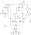
Figure 4 illustrates a modification of the Pierce oscillator ofFigure 3 to reduce noise and ensure a 50/50 duty cycle in the output voltage in accordance with the invention. -
Figure 5 is a flowchart for a method of operation of a Pierce oscillator in accordance with some but not all steps of the claimed inventive method. - Embodiments of the present disclosure and their advantages are best understood by referring to the detailed description that follows. It should be appreciated that like reference numerals are used to identify like elements illustrated in one or more of the figures.
- A Pierce oscillator is provided in which the DC gate and drain voltages for a first transistor are decoupled through a decoupling capacitor. An operational amplifier regulates the DC drain voltage to equal a desired value set by a reference voltage. The DC drain voltage may thus be regulated to, for example, one-half the power supply voltage to maximize the output voltage swing. In contrast, the DC gate voltage is determined by a channel size for the first transistor and a bias current driven into the first transistor. In this fashion, the transconductance gain for the first transistor may be optimized by biasing the first transistor in the subthreshold region. The resulting high gain and DC drain voltage regulation maximizes the output voltage swing. For example, in some embodiments the output voltage swing may be full rail, i.e., from ground to the power supply voltage. Moreover, the subthreshold operation also minimizes power consumption by the first transistor.
- An example Pierce
oscillator 200 is shown inFigure 2 . Crystal 105, transistor Mn1, and load capacitors C1 and C2 are arranged as discussed with regard toFigure 1 . A resistor R2 connect between the drain for transistor Mn1 to a positive input terminal for anoperational amplifier 205 that receives a reference voltage Vref at its negative input terminal. There is no DC current through resistor R2 so there is no DC voltage across resistor R2 such that the drain voltage Vd for transistor Mn1 is received at the positive input terminal foroperational amplifier 205. Similarly, there is no DC current across a resistor R1 that connects from the positive input terminal foroperational amplifier 205 to aterminal 215 for a load capacitor C1.Operational amplifier 205 controls an AC gate voltage for transistor Mn1 through a bias resistor Rbs. The high gain feedback throughoperational amplifier 205 thus regulates a voltage for its positive input terminal to equal the reference voltage. Since there is no DC current through the voltage divider resistor R2 during normal operation, both of its terminals are regulated to the reference voltage. Given that one of the terminals for resistor R2 is tied to the drain of transistor Mn1, the drain voltage Vd for transistor Mn1 is thus regulated to equal the reference voltage. - Since there is also no DC current through resistor R1, a voltage Vg2 for
terminal 215 is regulated to equal the reference voltage. To prevent the reference voltage from biasing the DC gate voltage for transistor Mn1, a decoupling capacitor C3 connects the gate of transistor Mn1 toterminal 215. Decoupling capacitor C3 thus also isolates the DC drain voltage of transistor Mn1 from its DC gate voltage. To reduce noise fromoperational amplifier 205, its output terminal is loaded by a feedback capacitor Cfb that connects to ground. The DC gate voltage for transistor Mn1 is set by the channel size for transistor Mn1 and a bias current IB from acurrent source 210 that drives the bias current into the drain terminal for transistor Mn1. Bias current IB and the channel size may thus be selected such that transistor Mn1 is biased for subthreshold operation. An AC portion for the gate voltage for transistor Mn1 is driven by an oscillating voltage fromcrystal 105 that couples through decoupling capacitor C3. It is this oscillating drive fromcrystal 105 that is subject to the transconductance gain for transistor Mn1. In one embodiment,operational amplifier 205 may be deemed to form a means for biasing the DC drain voltage of transistor Mn1 to equal the reference voltage. - As discussed earlier, the power consumption (current dissipated) through transistor Mn1 is minimized by its advantageous biasing in the subthreshold region yet the output voltage swing for the AC drain voltage is maximized by regulating the DC drain voltage to equal the reference voltage. Additional power reduction and gain enhancement may be achieved by modifying
Pierce oscillator 200 to include a PMOS transistor Mp1 in its current source as shown for aPierce oscillator 300 inFigure 3 . The source of transistor Mp1 connects to a power supply node supplying the power supply voltage VDD whereas its drain connects to the drain of transistor Mn1. Transistor Mp1 has its gate connected to a gate of a diode-connected PMOS transistor Mp2 through a resistor Rbs2. The source of diode-connected transistor Mp2 connects to the power supply node whereas its gate and drain are biased by acurrent source 305. Transistors Mp1 and Mp2 thus form a current mirror such that transistor Mp1 will conduct the same current as conducted by current source 305 (assuming that transistors Mp1 and Mp2 are matched). The voltage Vg2 atterminal 215 has the AC signal produced by the oscillation ofcrystal 105 that determines the transconductance gain for transistor Mn1. This AC signal will thus pass through a decoupling capacitor C4 that connects betweenterminal 215 and the gate of transistor Mp1. A gate voltage Vgp for transistor Mp1 will thus have the same AC signal applied to the gate of transistor Mn1 such that transistor Mp1 also contributes to the overall transconductance gain forPierce oscillator 300. This increase in transconductance gain is quite advantageous at increasing the output voltage swing at the drains of transistors Mp1 and Mn1. It will be appreciated that transistors Mp1 and Mp2 may have their gates directly connected without the inclusion of resistor Rbs2 in alternative embodiments. But note that the impedance at the gate of transistor Mp2 is somewhat low due to its diode connection to its drain. Decoupling capacitor C4 would then need a larger capacitance to AC couple voltage Vg2 to the gate of transistor Mp1. Resistor Rbs2 thus advantageously increases the impedance at the gate of transistor Mp1 such that a smaller decoupling capacitor C4 may be used. - Not only does transistor Mp1 contribute to the transconductance gain, it acts in concert with transistor Mn1 to limit the current dissipation. For example, during the oscillation of the drain voltage Vd, this drain voltage may rise towards the power supply voltage VDD. Transistor Mp1 is then pushed into the deep triode region of operation. But the gate voltage for transistor Mn1 is then driven towards ground such that transistor Mn1 shuts off to limit current dissipation. A similar choking of the current dissipation occurs as the drain voltage Vd oscillates towards ground such that transistor Mp1 essentially shuts off. Transistor Mp1 thus not only increases the transconductance gain but also limits the current consumption.
-
Pierce oscillator 300 may be further modified to reduce noise in the output voltage oscillation and improve its duty cycle as will be discussed with regard to aPierce oscillator 400 shown inFigure 4 . Rather than use the drain voltage Vd as the output voltage, the output voltage is instead sourced from voltage Vg2 atterminal 215. As compared to the drain voltage Vd, voltage Vg2 has less noise due to the filtering throughcrystal 105. To produce the output voltage (Out), afirst inverter 405 inverts voltage Vg2 to drive an input of asecond inverter 410 that produces the output voltage. The output voltage will thus be a square wave that oscillates at the oscillation frequency set bycrystal 105 and load capacitors C1 and C2. - To assure a 50/50 duty cycle for the oscillation of the output voltage, the reference voltage used by
operational amplifier 205 may be generated by an inverter formed by a serial stack of a PMOS transistor Mp3 and an NMOS transistor Mn2.Inverters node 415 for supplying the reference voltage connects to the gates of transistors Mp3 and Mn2. In addition,node 415 connects to the drains for transistor Mp3 and Mn2 through a resistor Rref At a power-up of the power supply voltage VDD, the reference voltage will initially be ground such that transistor Mp3is initially on to charge its drain towards the power supply voltage VDD. This increase in the drain voltage feeds back through resistor Rref to partially switch on transistor Mn2 and partially switch off transistor Mp3. The result will be that the reference voltage will stabilize at the trip point (threshold voltage) forinverters Figures 2 ,3 , and4 may be integrated within an integrated circuit such as a system-on-a-chip (SoC) with the exception ofcrystal 105. The resulting integrated circuit may then be integrated withcrystal 105 in a semiconductor package. It will be appreciated, however, that load capacitors C0 and C1 may be more readily implemented as external devices due to their relatively large capacitances such that they would also not be integrated into the integrated circuit in some embodiments. - A method of operation for a Pierce oscillator will now be discussed with regard to the flowchart of
Figure 5 . The method includes anact 500 of biasing a direct current (DC) gate voltage for a gate of a transconductance amplifier transistor in a Pierce oscillator by driving a drain terminal of the transconductance amplifier transistor with a current from a current source. The DC biasing of transistor Mn1 inoscillators act 500. The method further includes anact 505 of isolating the gate from the drain terminal through a decoupling capacitor. The function of decoupling capacitor C3 is an example ofact 505. Finally, the method includes anact 510 of amplifying a difference between a reference voltage and a DC drain voltage for the drain terminal to bias an alternating current (AC) gate voltage for the gate to cause the DC drain voltage to equal the reference voltage. The biasing of the gate of transistor Mn1 byoperational amplifier 205 is an example ofact 510. - It will thus be appreciated that many modifications and variations can be made in and to the materials, apparatus, configurations and methods of use of the devices of the present disclosure without departing from the scope thereof. In light of this, the scope of the present disclosure should not be limited to that of the particular embodiments illustrated and described herein, as they are merely by way of some examples thereof, but rather, should be fully commensurate with that of the claims appended hereafter and their functional equivalents.
Claims (11)
- A circuit, comprising:a first transistor (Mn1);a current source (305) for driving a drain of the first transistor (Mn1) with a bias current;a first decoupling capacitor (C3) for isolating a direct current, DC, drain voltage of the first transistor (Mn1) from a DC gate voltage of the first transistor, wherein a gate of the first transistor (Mn1) is configured to be driven by an AC input voltage from a crystal through the first decoupling capacitor (C3);an operational amplifier (205) configured to further bias the gate of the first transistor (Mn1) to regulate the DC drain voltage of the first transistor;a voltage divider having a first resistor (R2) having a first terminal connected to the drain of the first transistor and having a second terminal connected to a first terminal of a second resistor (R1), wherein the operational amplifier (205) has a first input connected to the second terminal of the first resistor (R2) and has a second input connected to a reference voltage node (415) for carrying a reference voltage, wherein a second terminal of the voltage divider is coupled to a terminal of the first decoupling capacitor (C3); the circuit being characterized in that it further comprisesa third inverter comprising a reference PMOS transistor (Mp3) having a source connected to a power supply node (VDD) for supplying a power supply voltage, a reference NMOS transistor (Mn2) having a source connected to ground and having a drain connected to a drain for the reference PMOS transistor (Mp3), and a reference resistor (RREF) connected between the drain of the reference NMOS transistor (Mn2) and the reference voltage node for supplying the reference voltage, wherein the reference voltage node is connected to a gate of the reference PMOS transistor (Mp3) and to a gate of the reference NMOS transistor (Mn2);a first inverter (405) configured to invert a voltage of the terminal of the first decoupling capacitor (C3); anda second inverter (410) configured to invert an output signal of the first inverter (405) to provide an output voltage (Out) for the circuit,wherein the PMOS and NMOS transistors in the third inverter are matched to respective transistors in the first inverter and second inverter each being formed by an analogous serial stack of a PMOS transistor and an NMOS transistor.
- The circuit of claim 1, wherein the first input is a positive input for the operational amplifier (205), and wherein the second input is a negative input for the operational amplifier (205).
- The circuit of claim 1, further comprising a biasing resistor (Rbs) coupled between an output of the operational amplifier and the gate of the first transistor.
- The circuit of claim 3, further comprising a feedback capacitor (Cfb) coupled between the output of the operational amplifier (205) and ground.
- The circuit of claim 1, wherein the first transistor (Mn1) is an NMOS transistor having a source connected to ground, and wherein the current source comprises a PMOS current source transistor (Mp1) having a source connected to a power supply node for supplying a power supply voltage and a drain connected to the drain of the NMOS transistor.
- The circuit of claim 5, further comprising a second decoupling capacitor (C4) coupled between the terminal of the first decoupling capacitor (C3) and a gate of the PMOS current source transistor.
- The circuit of claim 5, further comprising:a diode-connected PMOS transistor (Mp2) having a gate coupled to the gate of the PMOS current source transistor; anda current source coupled between a drain of the diode-connected PMOS transistor (Mp2) and ground.
- The circuit of claim 7, further comprising a bias resistor (Rbs2) configured to couple the gate of the diode-connected PMOS transistor to the gate of the PMOS current source transistor.
- The circuit of claim 1, wherein the circuit is integrated within an integrated circuit in a circuit package, the circuit package further comprising a crystal having a first terminal connected to the drain of the first transistor and having a second terminal connected to the terminal of the first decoupling capacitor.
- A method of oscillating an output signal, comprising:biasing (500) a direct current, DC, gate voltage of a gate of a first transistor in a Pierce oscillator by driving a drain of the first transistor with a current from a current source;isolating (505) the gate from the drain through a first decoupling capacitor;generating a reference voltage using a third inverter such that the reference voltage equals a threshold voltage for the third inverter;amplifying (510) a difference between the reference voltage and a voltage of a first terminal of a second resistor (R1), said voltage being generated by a voltage divider having a first resistor (R2) having a first terminal connected to the drain of the first transistor and having a second terminal connected to said first terminal of said second resistor (R1), to bias the gate of the first transistor to cause the DC drain voltage of the first transistor to equal the reference voltage divided by said voltage divider;driving the gate of the first transistor with an oscillating voltage from a crystal through the first decoupling capacitor;inverting the oscillating voltage in a first inverter to form an inverter output signal; andinverting the inverter output signal in a second inverter to form an oscillating output signal, wherein PMOS and NMOS transistors in the third inverter are matched to the respective transistors in the first and second inverter each being formed by an analogous serial stack of a PMOS transistor and an NMOS transistor.
- The method of claim 10, further comprising:generating the current from the current source in a second transistor; andcoupling the oscillating voltage from the crystal through a second decoupling capacitor to a gate of the second transistor.
Applications Claiming Priority (2)
| Application Number | Priority Date | Filing Date | Title |
|---|---|---|---|
| US15/649,475 US10483913B2 (en) | 2017-07-13 | 2017-07-13 | Low power crystal oscillator |
| PCT/US2018/039345 WO2019013964A1 (en) | 2017-07-13 | 2018-06-25 | Low power crystal oscillator |
Publications (2)
| Publication Number | Publication Date |
|---|---|
| EP3652856A1 EP3652856A1 (en) | 2020-05-20 |
| EP3652856B1 true EP3652856B1 (en) | 2023-05-10 |
Family
ID=63047432
Family Applications (1)
| Application Number | Title | Priority Date | Filing Date |
|---|---|---|---|
| EP18747047.1A Active EP3652856B1 (en) | 2017-07-13 | 2018-06-25 | Low power crystal oscillator |
Country Status (9)
| Country | Link |
|---|---|
| US (1) | US10483913B2 (en) |
| EP (1) | EP3652856B1 (en) |
| JP (2) | JP7000550B2 (en) |
| KR (1) | KR102141585B1 (en) |
| CN (1) | CN110870199B (en) |
| BR (1) | BR112020000298A2 (en) |
| SG (1) | SG11201911640YA (en) |
| TW (1) | TWI689172B (en) |
| WO (1) | WO2019013964A1 (en) |
Families Citing this family (6)
| Publication number | Priority date | Publication date | Assignee | Title |
|---|---|---|---|---|
| BR112020011035A2 (en) | 2017-11-17 | 2020-11-17 | Fraunhofer-Gesellschaft zur Förderung der angewandten Forschung e. V. | apparatus and method for encoding or decoding directional audio encoding parameters using different time-frequency resolutions |
| CN111555717B (en) * | 2020-06-15 | 2023-05-12 | 深圳职业技术学院 | A crystal oscillator circuit with built-in capacitor |
| JP6967248B1 (en) * | 2020-07-22 | 2021-11-17 | 大学共同利用機関法人 高エネルギー加速器研究機構 | Oscillator circuits and electronic devices |
| CN111953315B (en) * | 2020-09-08 | 2024-02-20 | 深圳市汇顶科技股份有限公司 | Crystal oscillator, chip and electronic device |
| CN112511155B (en) * | 2020-11-06 | 2023-10-10 | 深圳市国微电子有限公司 | Power supply voltage self-adaptive crystal oscillator driving circuit and oscillator |
| CN115296616B (en) * | 2022-03-10 | 2025-11-14 | 深圳市汇顶科技股份有限公司 | An oscillator acceleration circuit, chip, and electronic device |
Family Cites Families (19)
| Publication number | Priority date | Publication date | Assignee | Title |
|---|---|---|---|---|
| US4710730A (en) * | 1987-03-20 | 1987-12-01 | Motorola, Inc. | Data clock oscillator having accurate duty cycle |
| US5113156A (en) | 1991-04-22 | 1992-05-12 | Motorola, Inc. | Low power crystal oscillator with automatic gain control |
| EP1378995B1 (en) * | 1997-01-22 | 2006-11-08 | Seiko Epson Corporation | Oscillation circuit, constant voltage generation circuit, semiconductor device, electronic equipment and timepiece |
| US6028491A (en) * | 1998-04-29 | 2000-02-22 | Atmel Corporation | Crystal oscillator with controlled duty cycle |
| US6016081A (en) * | 1998-07-17 | 2000-01-18 | O'shaughnessy; Timothy G. | Tunable oscillator using a reference input frequency |
| US6664865B2 (en) * | 2001-05-11 | 2003-12-16 | Sequoia Communications | Amplitude-adjustable oscillator |
| KR100500928B1 (en) | 2002-06-29 | 2005-07-14 | 주식회사 하이닉스반도체 | Circuit for detecting switching point and semiconductor device using the same |
| US7292114B2 (en) * | 2005-08-01 | 2007-11-06 | Marvell World Trade Ltd. | Low-noise high-stability crystal oscillator |
| US7355489B2 (en) * | 2006-02-10 | 2008-04-08 | Cypress Semiconductor Corp. | High gain, high frequency CMOS oscillator circuit and method |
| JP2008035302A (en) * | 2006-07-31 | 2008-02-14 | Kawasaki Microelectronics Kk | Oscillation circuit including output circuit |
| EP2073377A1 (en) * | 2007-12-19 | 2009-06-24 | The Swatch Group Research and Development Ltd. | Oscillating quartz circuit with low consumption and active biasing |
| JP2010108419A (en) * | 2008-10-31 | 2010-05-13 | Toshiba Corp | Reference voltage generating circuit and regulator using the same |
| US8451071B2 (en) | 2008-11-24 | 2013-05-28 | Raytheon Company | Low noise oscillators |
| US20100259335A1 (en) * | 2009-04-13 | 2010-10-14 | Microchip Technology Incorporated | Resistorless feedback biasing for ultra low power crystal oscillator |
| US8704605B1 (en) | 2011-01-19 | 2014-04-22 | Marvell International Ltd. | Class-AB XTAL circuit |
| CN104253587B (en) | 2013-06-27 | 2017-10-20 | 上海东软载波微电子有限公司 | Crystal oscillator |
| JP2015023548A (en) * | 2013-07-23 | 2015-02-02 | ルネサスエレクトロニクス株式会社 | Semiconductor device |
| WO2015106195A1 (en) | 2014-01-10 | 2015-07-16 | University Of Virginia | A low voltage crystal oscillator (xtal) driver with feedback controlled duty cycling for ultra low power |
| US9209747B1 (en) | 2015-02-05 | 2015-12-08 | Freescale Semiconductor, Inc. | Crystal oscillator with resistorless feedback biasing |
-
2017
- 2017-07-13 US US15/649,475 patent/US10483913B2/en active Active
-
2018
- 2018-06-19 TW TW107120923A patent/TWI689172B/en active
- 2018-06-25 EP EP18747047.1A patent/EP3652856B1/en active Active
- 2018-06-25 SG SG11201911640YA patent/SG11201911640YA/en unknown
- 2018-06-25 KR KR1020207000803A patent/KR102141585B1/en active Active
- 2018-06-25 WO PCT/US2018/039345 patent/WO2019013964A1/en not_active Ceased
- 2018-06-25 JP JP2020501274A patent/JP7000550B2/en active Active
- 2018-06-25 CN CN201880045676.9A patent/CN110870199B/en active Active
- 2018-06-25 BR BR112020000298-4A patent/BR112020000298A2/en not_active Application Discontinuation
-
2020
- 2020-11-27 JP JP2020196774A patent/JP2021048612A/en not_active Withdrawn
Also Published As
| Publication number | Publication date |
|---|---|
| JP2021048612A (en) | 2021-03-25 |
| BR112020000298A2 (en) | 2020-07-14 |
| SG11201911640YA (en) | 2020-01-30 |
| EP3652856A1 (en) | 2020-05-20 |
| US20190020309A1 (en) | 2019-01-17 |
| KR102141585B1 (en) | 2020-08-05 |
| CN110870199A (en) | 2020-03-06 |
| CN110870199B (en) | 2023-10-20 |
| TWI689172B (en) | 2020-03-21 |
| KR20200009122A (en) | 2020-01-29 |
| JP2020526987A (en) | 2020-08-31 |
| JP7000550B2 (en) | 2022-01-19 |
| US10483913B2 (en) | 2019-11-19 |
| WO2019013964A1 (en) | 2019-01-17 |
| TW201918017A (en) | 2019-05-01 |
Similar Documents
| Publication | Publication Date | Title |
|---|---|---|
| CN110870199B (en) | low power crystal oscillator | |
| US6859112B2 (en) | CMOS voltage controlled oscillator circuit for operation with low supply voltage and method for same | |
| US10848102B2 (en) | Crystal oscillator | |
| JP4536364B2 (en) | High quality parallel resonant oscillator | |
| US20160181978A1 (en) | Compensation circuit and inverter stage for oscillator circuit | |
| US20120223781A1 (en) | Noise regulated linear voltage controlled oscillator | |
| US7183868B1 (en) | Triple inverter pierce oscillator circuit suitable for CMOS | |
| US10778145B2 (en) | Magnetically pumped voltage controlled oscillator | |
| US20080238561A1 (en) | Piezoelectric oscillator | |
| JP2002290230A (en) | Cmos inverter | |
| JP4259241B2 (en) | Oscillation circuit and semiconductor integrated circuit | |
| KR101415733B1 (en) | Voltage controlled oscillator | |
| JP3937781B2 (en) | Crystal oscillation circuit | |
| US20150137898A1 (en) | Oscillator Buffer and Method for Calibrating the Same | |
| US7768358B2 (en) | Oscillatory signal output circuit for capacitive coupling an oscillating signal with bias voltage applied | |
| HK40017276A (en) | Low power crystal oscillator | |
| US5914643A (en) | Source coupled CMOS crystal oscillator | |
| JP6611007B2 (en) | Level shift circuit | |
| JP2008035302A (en) | Oscillation circuit including output circuit | |
| JP2001217652A (en) | Crystal oscillation circuit | |
| JP2000244245A (en) | Oscillator circuit | |
| JP2001156600A (en) | Oscillator | |
| JP2010193330A (en) | Oscillator |
Legal Events
| Date | Code | Title | Description |
|---|---|---|---|
| STAA | Information on the status of an ep patent application or granted ep patent |
Free format text: STATUS: UNKNOWN |
|
| STAA | Information on the status of an ep patent application or granted ep patent |
Free format text: STATUS: THE INTERNATIONAL PUBLICATION HAS BEEN MADE |
|
| PUAI | Public reference made under article 153(3) epc to a published international application that has entered the european phase |
Free format text: ORIGINAL CODE: 0009012 |
|
| STAA | Information on the status of an ep patent application or granted ep patent |
Free format text: STATUS: REQUEST FOR EXAMINATION WAS MADE |
|
| 17P | Request for examination filed |
Effective date: 20191204 |
|
| AK | Designated contracting states |
Kind code of ref document: A1 Designated state(s): AL AT BE BG CH CY CZ DE DK EE ES FI FR GB GR HR HU IE IS IT LI LT LU LV MC MK MT NL NO PL PT RO RS SE SI SK SM TR |
|
| AX | Request for extension of the european patent |
Extension state: BA ME |
|
| DAV | Request for validation of the european patent (deleted) | ||
| DAX | Request for extension of the european patent (deleted) | ||
| GRAP | Despatch of communication of intention to grant a patent |
Free format text: ORIGINAL CODE: EPIDOSNIGR1 |
|
| STAA | Information on the status of an ep patent application or granted ep patent |
Free format text: STATUS: GRANT OF PATENT IS INTENDED |
|
| INTG | Intention to grant announced |
Effective date: 20220914 |
|
| GRAJ | Information related to disapproval of communication of intention to grant by the applicant or resumption of examination proceedings by the epo deleted |
Free format text: ORIGINAL CODE: EPIDOSDIGR1 |
|
| STAA | Information on the status of an ep patent application or granted ep patent |
Free format text: STATUS: REQUEST FOR EXAMINATION WAS MADE |
|
| GRAP | Despatch of communication of intention to grant a patent |
Free format text: ORIGINAL CODE: EPIDOSNIGR1 |
|
| STAA | Information on the status of an ep patent application or granted ep patent |
Free format text: STATUS: GRANT OF PATENT IS INTENDED |
|
| INTC | Intention to grant announced (deleted) | ||
| INTG | Intention to grant announced |
Effective date: 20230215 |
|
| GRAS | Grant fee paid |
Free format text: ORIGINAL CODE: EPIDOSNIGR3 |
|
| GRAA | (expected) grant |
Free format text: ORIGINAL CODE: 0009210 |
|
| STAA | Information on the status of an ep patent application or granted ep patent |
Free format text: STATUS: THE PATENT HAS BEEN GRANTED |
|
| AK | Designated contracting states |
Kind code of ref document: B1 Designated state(s): AL AT BE BG CH CY CZ DE DK EE ES FI FR GB GR HR HU IE IS IT LI LT LU LV MC MK MT NL NO PL PT RO RS SE SI SK SM TR |
|
| REG | Reference to a national code |
Ref country code: GB Ref legal event code: FG4D |
|
| REG | Reference to a national code |
Ref country code: AT Ref legal event code: REF Ref document number: 1567725 Country of ref document: AT Kind code of ref document: T Effective date: 20230515 Ref country code: CH Ref legal event code: EP |
|
| REG | Reference to a national code |
Ref country code: DE Ref legal event code: R096 Ref document number: 602018049620 Country of ref document: DE |
|
| REG | Reference to a national code |
Ref country code: IE Ref legal event code: FG4D |
|
| REG | Reference to a national code |
Ref country code: NL Ref legal event code: FP |
|
| REG | Reference to a national code |
Ref country code: LT Ref legal event code: MG9D |
|
| REG | Reference to a national code |
Ref country code: AT Ref legal event code: MK05 Ref document number: 1567725 Country of ref document: AT Kind code of ref document: T Effective date: 20230510 |
|
| PG25 | Lapsed in a contracting state [announced via postgrant information from national office to epo] |
Ref country code: SE Free format text: LAPSE BECAUSE OF FAILURE TO SUBMIT A TRANSLATION OF THE DESCRIPTION OR TO PAY THE FEE WITHIN THE PRESCRIBED TIME-LIMIT Effective date: 20230510 Ref country code: PT Free format text: LAPSE BECAUSE OF FAILURE TO SUBMIT A TRANSLATION OF THE DESCRIPTION OR TO PAY THE FEE WITHIN THE PRESCRIBED TIME-LIMIT Effective date: 20230911 Ref country code: NO Free format text: LAPSE BECAUSE OF FAILURE TO SUBMIT A TRANSLATION OF THE DESCRIPTION OR TO PAY THE FEE WITHIN THE PRESCRIBED TIME-LIMIT Effective date: 20230810 Ref country code: ES Free format text: LAPSE BECAUSE OF FAILURE TO SUBMIT A TRANSLATION OF THE DESCRIPTION OR TO PAY THE FEE WITHIN THE PRESCRIBED TIME-LIMIT Effective date: 20230510 Ref country code: AT Free format text: LAPSE BECAUSE OF FAILURE TO SUBMIT A TRANSLATION OF THE DESCRIPTION OR TO PAY THE FEE WITHIN THE PRESCRIBED TIME-LIMIT Effective date: 20230510 |
|
| PG25 | Lapsed in a contracting state [announced via postgrant information from national office to epo] |
Ref country code: RS Free format text: LAPSE BECAUSE OF FAILURE TO SUBMIT A TRANSLATION OF THE DESCRIPTION OR TO PAY THE FEE WITHIN THE PRESCRIBED TIME-LIMIT Effective date: 20230510 Ref country code: PL Free format text: LAPSE BECAUSE OF FAILURE TO SUBMIT A TRANSLATION OF THE DESCRIPTION OR TO PAY THE FEE WITHIN THE PRESCRIBED TIME-LIMIT Effective date: 20230510 Ref country code: LV Free format text: LAPSE BECAUSE OF FAILURE TO SUBMIT A TRANSLATION OF THE DESCRIPTION OR TO PAY THE FEE WITHIN THE PRESCRIBED TIME-LIMIT Effective date: 20230510 Ref country code: LT Free format text: LAPSE BECAUSE OF FAILURE TO SUBMIT A TRANSLATION OF THE DESCRIPTION OR TO PAY THE FEE WITHIN THE PRESCRIBED TIME-LIMIT Effective date: 20230510 Ref country code: IS Free format text: LAPSE BECAUSE OF FAILURE TO SUBMIT A TRANSLATION OF THE DESCRIPTION OR TO PAY THE FEE WITHIN THE PRESCRIBED TIME-LIMIT Effective date: 20230910 Ref country code: HR Free format text: LAPSE BECAUSE OF FAILURE TO SUBMIT A TRANSLATION OF THE DESCRIPTION OR TO PAY THE FEE WITHIN THE PRESCRIBED TIME-LIMIT Effective date: 20230510 Ref country code: GR Free format text: LAPSE BECAUSE OF FAILURE TO SUBMIT A TRANSLATION OF THE DESCRIPTION OR TO PAY THE FEE WITHIN THE PRESCRIBED TIME-LIMIT Effective date: 20230811 |
|
| PG25 | Lapsed in a contracting state [announced via postgrant information from national office to epo] |
Ref country code: FI Free format text: LAPSE BECAUSE OF FAILURE TO SUBMIT A TRANSLATION OF THE DESCRIPTION OR TO PAY THE FEE WITHIN THE PRESCRIBED TIME-LIMIT Effective date: 20230510 |
|
| PG25 | Lapsed in a contracting state [announced via postgrant information from national office to epo] |
Ref country code: SK Free format text: LAPSE BECAUSE OF FAILURE TO SUBMIT A TRANSLATION OF THE DESCRIPTION OR TO PAY THE FEE WITHIN THE PRESCRIBED TIME-LIMIT Effective date: 20230510 |
|
| PG25 | Lapsed in a contracting state [announced via postgrant information from national office to epo] |
Ref country code: SM Free format text: LAPSE BECAUSE OF FAILURE TO SUBMIT A TRANSLATION OF THE DESCRIPTION OR TO PAY THE FEE WITHIN THE PRESCRIBED TIME-LIMIT Effective date: 20230510 Ref country code: SK Free format text: LAPSE BECAUSE OF FAILURE TO SUBMIT A TRANSLATION OF THE DESCRIPTION OR TO PAY THE FEE WITHIN THE PRESCRIBED TIME-LIMIT Effective date: 20230510 Ref country code: RO Free format text: LAPSE BECAUSE OF FAILURE TO SUBMIT A TRANSLATION OF THE DESCRIPTION OR TO PAY THE FEE WITHIN THE PRESCRIBED TIME-LIMIT Effective date: 20230510 Ref country code: EE Free format text: LAPSE BECAUSE OF FAILURE TO SUBMIT A TRANSLATION OF THE DESCRIPTION OR TO PAY THE FEE WITHIN THE PRESCRIBED TIME-LIMIT Effective date: 20230510 Ref country code: DK Free format text: LAPSE BECAUSE OF FAILURE TO SUBMIT A TRANSLATION OF THE DESCRIPTION OR TO PAY THE FEE WITHIN THE PRESCRIBED TIME-LIMIT Effective date: 20230510 Ref country code: CZ Free format text: LAPSE BECAUSE OF FAILURE TO SUBMIT A TRANSLATION OF THE DESCRIPTION OR TO PAY THE FEE WITHIN THE PRESCRIBED TIME-LIMIT Effective date: 20230510 |
|
| REG | Reference to a national code |
Ref country code: CH Ref legal event code: PL |
|
| REG | Reference to a national code |
Ref country code: DE Ref legal event code: R097 Ref document number: 602018049620 Country of ref document: DE |
|
| REG | Reference to a national code |
Ref country code: BE Ref legal event code: MM Effective date: 20230630 |
|
| PG25 | Lapsed in a contracting state [announced via postgrant information from national office to epo] |
Ref country code: MC Free format text: LAPSE BECAUSE OF FAILURE TO SUBMIT A TRANSLATION OF THE DESCRIPTION OR TO PAY THE FEE WITHIN THE PRESCRIBED TIME-LIMIT Effective date: 20230510 |
|
| PG25 | Lapsed in a contracting state [announced via postgrant information from national office to epo] |
Ref country code: MC Free format text: LAPSE BECAUSE OF FAILURE TO SUBMIT A TRANSLATION OF THE DESCRIPTION OR TO PAY THE FEE WITHIN THE PRESCRIBED TIME-LIMIT Effective date: 20230510 |
|
| PG25 | Lapsed in a contracting state [announced via postgrant information from national office to epo] |
Ref country code: LU Free format text: LAPSE BECAUSE OF NON-PAYMENT OF DUE FEES Effective date: 20230625 |
|
| PLBE | No opposition filed within time limit |
Free format text: ORIGINAL CODE: 0009261 |
|
| STAA | Information on the status of an ep patent application or granted ep patent |
Free format text: STATUS: NO OPPOSITION FILED WITHIN TIME LIMIT |
|
| REG | Reference to a national code |
Ref country code: IE Ref legal event code: MM4A |
|
| PG25 | Lapsed in a contracting state [announced via postgrant information from national office to epo] |
Ref country code: LU Free format text: LAPSE BECAUSE OF NON-PAYMENT OF DUE FEES Effective date: 20230625 |
|
| PG25 | Lapsed in a contracting state [announced via postgrant information from national office to epo] |
Ref country code: IE Free format text: LAPSE BECAUSE OF NON-PAYMENT OF DUE FEES Effective date: 20230625 |
|
| 26N | No opposition filed |
Effective date: 20240213 |
|
| PG25 | Lapsed in a contracting state [announced via postgrant information from national office to epo] |
Ref country code: IE Free format text: LAPSE BECAUSE OF NON-PAYMENT OF DUE FEES Effective date: 20230625 Ref country code: CH Free format text: LAPSE BECAUSE OF NON-PAYMENT OF DUE FEES Effective date: 20230630 |
|
| PG25 | Lapsed in a contracting state [announced via postgrant information from national office to epo] |
Ref country code: SI Free format text: LAPSE BECAUSE OF FAILURE TO SUBMIT A TRANSLATION OF THE DESCRIPTION OR TO PAY THE FEE WITHIN THE PRESCRIBED TIME-LIMIT Effective date: 20230510 |
|
| PG25 | Lapsed in a contracting state [announced via postgrant information from national office to epo] |
Ref country code: SI Free format text: LAPSE BECAUSE OF FAILURE TO SUBMIT A TRANSLATION OF THE DESCRIPTION OR TO PAY THE FEE WITHIN THE PRESCRIBED TIME-LIMIT Effective date: 20230510 Ref country code: IT Free format text: LAPSE BECAUSE OF FAILURE TO SUBMIT A TRANSLATION OF THE DESCRIPTION OR TO PAY THE FEE WITHIN THE PRESCRIBED TIME-LIMIT Effective date: 20230510 Ref country code: BE Free format text: LAPSE BECAUSE OF NON-PAYMENT OF DUE FEES Effective date: 20230630 |
|
| PGFP | Annual fee paid to national office [announced via postgrant information from national office to epo] |
Ref country code: NL Payment date: 20240514 Year of fee payment: 7 |
|
| PG25 | Lapsed in a contracting state [announced via postgrant information from national office to epo] |
Ref country code: BG Free format text: LAPSE BECAUSE OF FAILURE TO SUBMIT A TRANSLATION OF THE DESCRIPTION OR TO PAY THE FEE WITHIN THE PRESCRIBED TIME-LIMIT Effective date: 20230510 |
|
| PG25 | Lapsed in a contracting state [announced via postgrant information from national office to epo] |
Ref country code: BG Free format text: LAPSE BECAUSE OF FAILURE TO SUBMIT A TRANSLATION OF THE DESCRIPTION OR TO PAY THE FEE WITHIN THE PRESCRIBED TIME-LIMIT Effective date: 20230510 |
|
| PGFP | Annual fee paid to national office [announced via postgrant information from national office to epo] |
Ref country code: DE Payment date: 20250509 Year of fee payment: 8 |
|
| PGFP | Annual fee paid to national office [announced via postgrant information from national office to epo] |
Ref country code: GB Payment date: 20250508 Year of fee payment: 8 |
|
| PGFP | Annual fee paid to national office [announced via postgrant information from national office to epo] |
Ref country code: FR Payment date: 20250512 Year of fee payment: 8 |
|
| PG25 | Lapsed in a contracting state [announced via postgrant information from national office to epo] |
Ref country code: CY Free format text: LAPSE BECAUSE OF FAILURE TO SUBMIT A TRANSLATION OF THE DESCRIPTION OR TO PAY THE FEE WITHIN THE PRESCRIBED TIME-LIMIT; INVALID AB INITIO Effective date: 20180625 |
|
| PG25 | Lapsed in a contracting state [announced via postgrant information from national office to epo] |
Ref country code: HU Free format text: LAPSE BECAUSE OF FAILURE TO SUBMIT A TRANSLATION OF THE DESCRIPTION OR TO PAY THE FEE WITHIN THE PRESCRIBED TIME-LIMIT; INVALID AB INITIO Effective date: 20180625 |
|
| PG25 | Lapsed in a contracting state [announced via postgrant information from national office to epo] |
Ref country code: TR Free format text: LAPSE BECAUSE OF FAILURE TO SUBMIT A TRANSLATION OF THE DESCRIPTION OR TO PAY THE FEE WITHIN THE PRESCRIBED TIME-LIMIT Effective date: 20230510 |
|
| REG | Reference to a national code |
Ref country code: NL Ref legal event code: MM Effective date: 20250701 |
|
| PG25 | Lapsed in a contracting state [announced via postgrant information from national office to epo] |
Ref country code: NL Free format text: LAPSE BECAUSE OF NON-PAYMENT OF DUE FEES Effective date: 20250701 |