EP3650939A1 - Prédiction d'une valeur d'un paramètre de processus de fabrication de semiconducteurs - Google Patents
Prédiction d'une valeur d'un paramètre de processus de fabrication de semiconducteurs Download PDFInfo
- Publication number
- EP3650939A1 EP3650939A1 EP18204882.7A EP18204882A EP3650939A1 EP 3650939 A1 EP3650939 A1 EP 3650939A1 EP 18204882 A EP18204882 A EP 18204882A EP 3650939 A1 EP3650939 A1 EP 3650939A1
- Authority
- EP
- European Patent Office
- Prior art keywords
- value
- parameter
- semiconductor manufacturing
- measurements
- manufacturing process
- Prior art date
- Legal status (The legal status is an assumption and is not a legal conclusion. Google has not performed a legal analysis and makes no representation as to the accuracy of the status listed.)
- Withdrawn
Links
- 238000004519 manufacturing process Methods 0.000 title claims abstract description 39
- 239000004065 semiconductor Substances 0.000 title claims abstract description 35
- 238000000034 method Methods 0.000 claims abstract description 78
- 238000005259 measurement Methods 0.000 claims abstract description 57
- 238000005070 sampling Methods 0.000 claims abstract description 38
- 238000013528 artificial neural network Methods 0.000 claims abstract description 13
- 230000000306 recurrent effect Effects 0.000 claims abstract description 9
- 230000006403 short-term memory Effects 0.000 claims abstract description 3
- 239000000758 substrate Substances 0.000 claims description 69
- 238000000059 patterning Methods 0.000 claims description 27
- 230000005855 radiation Effects 0.000 claims description 26
- 238000012545 processing Methods 0.000 claims description 10
- 238000005286 illumination Methods 0.000 claims description 6
- 238000004590 computer program Methods 0.000 claims description 4
- 235000012431 wafers Nutrition 0.000 description 30
- 238000012937 correction Methods 0.000 description 20
- 238000007689 inspection Methods 0.000 description 14
- 230000007547 defect Effects 0.000 description 8
- 238000013461 design Methods 0.000 description 7
- 230000003287 optical effect Effects 0.000 description 7
- 238000001459 lithography Methods 0.000 description 5
- 238000012549 training Methods 0.000 description 4
- 238000007654 immersion Methods 0.000 description 3
- 239000007788 liquid Substances 0.000 description 3
- 238000004140 cleaning Methods 0.000 description 2
- 230000003750 conditioning effect Effects 0.000 description 2
- 230000005670 electromagnetic radiation Effects 0.000 description 2
- 238000005457 optimization Methods 0.000 description 2
- 238000000206 photolithography Methods 0.000 description 2
- 238000004886 process control Methods 0.000 description 2
- 238000004088 simulation Methods 0.000 description 2
- 238000004422 calculation algorithm Methods 0.000 description 1
- 238000004364 calculation method Methods 0.000 description 1
- 238000001514 detection method Methods 0.000 description 1
- 238000009826 distribution Methods 0.000 description 1
- 230000009977 dual effect Effects 0.000 description 1
- 238000005516 engineering process Methods 0.000 description 1
- 238000005530 etching Methods 0.000 description 1
- 238000000671 immersion lithography Methods 0.000 description 1
- 230000003116 impacting effect Effects 0.000 description 1
- 239000004973 liquid crystal related substance Substances 0.000 description 1
- 230000005381 magnetic domain Effects 0.000 description 1
- 239000000463 material Substances 0.000 description 1
- 230000015654 memory Effects 0.000 description 1
- 238000001393 microlithography Methods 0.000 description 1
- 238000012986 modification Methods 0.000 description 1
- 230000004048 modification Effects 0.000 description 1
- 238000002360 preparation method Methods 0.000 description 1
- 230000035945 sensitivity Effects 0.000 description 1
- 238000007493 shaping process Methods 0.000 description 1
- 239000002904 solvent Substances 0.000 description 1
- 239000010409 thin film Substances 0.000 description 1
- 238000012546 transfer Methods 0.000 description 1
- XLYOFNOQVPJJNP-UHFFFAOYSA-N water Substances O XLYOFNOQVPJJNP-UHFFFAOYSA-N 0.000 description 1
Images


Classifications
-
- G—PHYSICS
- G03—PHOTOGRAPHY; CINEMATOGRAPHY; ANALOGOUS TECHNIQUES USING WAVES OTHER THAN OPTICAL WAVES; ELECTROGRAPHY; HOLOGRAPHY
- G03F—PHOTOMECHANICAL PRODUCTION OF TEXTURED OR PATTERNED SURFACES, e.g. FOR PRINTING, FOR PROCESSING OF SEMICONDUCTOR DEVICES; MATERIALS THEREFOR; ORIGINALS THEREFOR; APPARATUS SPECIALLY ADAPTED THEREFOR
- G03F7/00—Photomechanical, e.g. photolithographic, production of textured or patterned surfaces, e.g. printing surfaces; Materials therefor, e.g. comprising photoresists; Apparatus specially adapted therefor
- G03F7/70—Microphotolithographic exposure; Apparatus therefor
- G03F7/70483—Information management; Active and passive control; Testing; Wafer monitoring, e.g. pattern monitoring
- G03F7/70605—Workpiece metrology
- G03F7/70616—Monitoring the printed patterns
- G03F7/70633—Overlay, i.e. relative alignment between patterns printed by separate exposures in different layers, or in the same layer in multiple exposures or stitching
-
- G—PHYSICS
- G03—PHOTOGRAPHY; CINEMATOGRAPHY; ANALOGOUS TECHNIQUES USING WAVES OTHER THAN OPTICAL WAVES; ELECTROGRAPHY; HOLOGRAPHY
- G03F—PHOTOMECHANICAL PRODUCTION OF TEXTURED OR PATTERNED SURFACES, e.g. FOR PRINTING, FOR PROCESSING OF SEMICONDUCTOR DEVICES; MATERIALS THEREFOR; ORIGINALS THEREFOR; APPARATUS SPECIALLY ADAPTED THEREFOR
- G03F7/00—Photomechanical, e.g. photolithographic, production of textured or patterned surfaces, e.g. printing surfaces; Materials therefor, e.g. comprising photoresists; Apparatus specially adapted therefor
- G03F7/70—Microphotolithographic exposure; Apparatus therefor
- G03F7/70483—Information management; Active and passive control; Testing; Wafer monitoring, e.g. pattern monitoring
- G03F7/70491—Information management, e.g. software; Active and passive control, e.g. details of controlling exposure processes or exposure tool monitoring processes
- G03F7/705—Modelling or simulating from physical phenomena up to complete wafer processes or whole workflow in wafer productions
-
- G—PHYSICS
- G05—CONTROLLING; REGULATING
- G05B—CONTROL OR REGULATING SYSTEMS IN GENERAL; FUNCTIONAL ELEMENTS OF SUCH SYSTEMS; MONITORING OR TESTING ARRANGEMENTS FOR SUCH SYSTEMS OR ELEMENTS
- G05B13/00—Adaptive control systems, i.e. systems automatically adjusting themselves to have a performance which is optimum according to some preassigned criterion
- G05B13/02—Adaptive control systems, i.e. systems automatically adjusting themselves to have a performance which is optimum according to some preassigned criterion electric
- G05B13/0265—Adaptive control systems, i.e. systems automatically adjusting themselves to have a performance which is optimum according to some preassigned criterion electric the criterion being a learning criterion
- G05B13/027—Adaptive control systems, i.e. systems automatically adjusting themselves to have a performance which is optimum according to some preassigned criterion electric the criterion being a learning criterion using neural networks only
-
- G—PHYSICS
- G05—CONTROLLING; REGULATING
- G05B—CONTROL OR REGULATING SYSTEMS IN GENERAL; FUNCTIONAL ELEMENTS OF SUCH SYSTEMS; MONITORING OR TESTING ARRANGEMENTS FOR SUCH SYSTEMS OR ELEMENTS
- G05B19/00—Programme-control systems
- G05B19/02—Programme-control systems electric
- G05B19/418—Total factory control, i.e. centrally controlling a plurality of machines, e.g. direct or distributed numerical control [DNC], flexible manufacturing systems [FMS], integrated manufacturing systems [IMS] or computer integrated manufacturing [CIM]
- G05B19/41875—Total factory control, i.e. centrally controlling a plurality of machines, e.g. direct or distributed numerical control [DNC], flexible manufacturing systems [FMS], integrated manufacturing systems [IMS] or computer integrated manufacturing [CIM] characterised by quality surveillance of production
-
- H—ELECTRICITY
- H01—ELECTRIC ELEMENTS
- H01L—SEMICONDUCTOR DEVICES NOT COVERED BY CLASS H10
- H01L22/00—Testing or measuring during manufacture or treatment; Reliability measurements, i.e. testing of parts without further processing to modify the parts as such; Structural arrangements therefor
- H01L22/10—Measuring as part of the manufacturing process
- H01L22/12—Measuring as part of the manufacturing process for structural parameters, e.g. thickness, line width, refractive index, temperature, warp, bond strength, defects, optical inspection, electrical measurement of structural dimensions, metallurgic measurement of diffusions
-
- H—ELECTRICITY
- H01—ELECTRIC ELEMENTS
- H01L—SEMICONDUCTOR DEVICES NOT COVERED BY CLASS H10
- H01L22/00—Testing or measuring during manufacture or treatment; Reliability measurements, i.e. testing of parts without further processing to modify the parts as such; Structural arrangements therefor
- H01L22/20—Sequence of activities consisting of a plurality of measurements, corrections, marking or sorting steps
-
- G—PHYSICS
- G05—CONTROLLING; REGULATING
- G05B—CONTROL OR REGULATING SYSTEMS IN GENERAL; FUNCTIONAL ELEMENTS OF SUCH SYSTEMS; MONITORING OR TESTING ARRANGEMENTS FOR SUCH SYSTEMS OR ELEMENTS
- G05B2219/00—Program-control systems
- G05B2219/30—Nc systems
- G05B2219/32—Operator till task planning
- G05B2219/32193—Ann, neural base quality management
-
- G—PHYSICS
- G05—CONTROLLING; REGULATING
- G05B—CONTROL OR REGULATING SYSTEMS IN GENERAL; FUNCTIONAL ELEMENTS OF SUCH SYSTEMS; MONITORING OR TESTING ARRANGEMENTS FOR SUCH SYSTEMS OR ELEMENTS
- G05B2219/00—Program-control systems
- G05B2219/30—Nc systems
- G05B2219/32—Operator till task planning
- G05B2219/32194—Quality prediction
-
- G—PHYSICS
- G05—CONTROLLING; REGULATING
- G05B—CONTROL OR REGULATING SYSTEMS IN GENERAL; FUNCTIONAL ELEMENTS OF SUCH SYSTEMS; MONITORING OR TESTING ARRANGEMENTS FOR SUCH SYSTEMS OR ELEMENTS
- G05B2219/00—Program-control systems
- G05B2219/30—Nc systems
- G05B2219/33—Director till display
- G05B2219/33205—Coax or optical fiber or twisted pair
-
- G—PHYSICS
- G05—CONTROLLING; REGULATING
- G05B—CONTROL OR REGULATING SYSTEMS IN GENERAL; FUNCTIONAL ELEMENTS OF SUCH SYSTEMS; MONITORING OR TESTING ARRANGEMENTS FOR SUCH SYSTEMS OR ELEMENTS
- G05B2219/00—Program-control systems
- G05B2219/30—Nc systems
- G05B2219/45—Nc applications
- G05B2219/45028—Lithography
-
- Y—GENERAL TAGGING OF NEW TECHNOLOGICAL DEVELOPMENTS; GENERAL TAGGING OF CROSS-SECTIONAL TECHNOLOGIES SPANNING OVER SEVERAL SECTIONS OF THE IPC; TECHNICAL SUBJECTS COVERED BY FORMER USPC CROSS-REFERENCE ART COLLECTIONS [XRACs] AND DIGESTS
- Y02—TECHNOLOGIES OR APPLICATIONS FOR MITIGATION OR ADAPTATION AGAINST CLIMATE CHANGE
- Y02P—CLIMATE CHANGE MITIGATION TECHNOLOGIES IN THE PRODUCTION OR PROCESSING OF GOODS
- Y02P90/00—Enabling technologies with a potential contribution to greenhouse gas [GHG] emissions mitigation
- Y02P90/02—Total factory control, e.g. smart factories, flexible manufacturing systems [FMS] or integrated manufacturing systems [IMS]
Definitions
- the present invention relates to methods of predicting a value of parameter associated with a semiconductor manufacturing process, semiconductor manufacturing processes, lithographic apparatuses and associated computer program products.
- a lithographic apparatus is a machine constructed to apply a desired pattern onto a substrate.
- a lithographic apparatus can be used, for example, in the manufacture of integrated circuits (ICs).
- a lithographic apparatus may, for example, project a pattern (also often referred to as "design layout" or "design") at a patterning device (e.g., a mask) onto a layer of radiation-sensitive material (resist) provided on a substrate (e.g., a wafer).
- a lithographic apparatus may use electromagnetic radiation.
- the wavelength of this radiation determines the minimum size of features which can be formed on the substrate. Typical wavelengths currently in use are 365 nm (i-line), 248 nm, 193 nm and 13.5 nm.
- a lithographic apparatus which uses extreme ultraviolet (EUV) radiation, having a wavelength within the range 4-20 nm, for example 6.7 nm or 13.5 nm, may be used to form smaller features on a substrate than a lithographic apparatus which uses, for example, radiation with a wavelength of 193 nm.
- EUV extreme ultraviolet
- Low-ki lithography may be used to process features with dimensions smaller than the classical resolution limit of a lithographic apparatus.
- k 1 the more difficult it becomes to reproduce the pattern on the substrate that resembles the shape and dimensions planned by a circuit designer in order to achieve particular electrical functionality and performance.
- sophisticated fine-tuning steps may be applied to the lithographic projection apparatus and/or design layout.
- RET resolution enhancement techniques
- a method for predicting a value of first parameter associated with a semiconductor manufacturing process comprising:
- the method further comprises using the predicted value of the first parameter determined based on the first value obtained from measurements at a first operation of a process step in the semiconductor manufacturing process to determine a control recipe of a subsequent operation of the process step in the semiconductor manufacturing process.
- a semiconductor manufacturing process comprising a method for predicting a value of a parameter associated with the semiconductor manufacturing process according to the method of any preceding claim.
- a lithographic apparatus comprising:
- a computer program product comprising machine readable instructions for causing a general-purpose data processing apparatus to perform the steps of a method of the first aspect.
- the terms "radiation” and “beam” are used to encompass all types of electromagnetic radiation, including ultraviolet radiation (e.g. with a wavelength of 365, 248, 193, 157 or 126 nm) and EUV (extreme ultra-violet radiation, e.g. having a wavelength in the range of about 5-100 nm).
- ultraviolet radiation e.g. with a wavelength of 365, 248, 193, 157 or 126 nm
- EUV extreme ultra-violet radiation
- reticle may be broadly interpreted as referring to a generic patterning device that can be used to endow an incoming radiation beam with a patterned cross-section, corresponding to a pattern that is to be created in a target portion of the substrate.
- the term “light valve” can also be used in this context.
- examples of other such patterning devices include a programmable mirror array and a programmable LCD array.
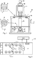
- FIG. 1 schematically depicts a lithographic apparatus LA.
- the lithographic apparatus LA includes an illumination system (also referred to as illuminator) IL configured to condition a radiation beam B (e.g., UV radiation, DUV radiation or EUV radiation), a mask support (e.g., a mask table) MT constructed to support a patterning device (e.g., a mask) MA and connected to a first positioner PM configured to accurately position the patterning device MA in accordance with certain parameters, a substrate support (e.g., a wafer table) WT constructed to hold a substrate (e.g., a resist coated wafer) W and connected to a second positioner PW configured to accurately position the substrate support in accordance with certain parameters, and a projection system (e.g., a refractive projection lens system) PS configured to project a pattern imparted to the radiation beam B by patterning device MA onto a target portion C (e.g., comprising one or more dies) of the substrate W.
- the illumination system IL receives a radiation beam from a radiation source SO, e.g. via a beam delivery system BD.
- the illumination system IL may include various types of optical components, such as refractive, reflective, magnetic, electromagnetic, electrostatic, and/or other types of optical components, or any combination thereof, for directing, shaping, and/or controlling radiation.
- the illuminator IL may be used to condition the radiation beam B to have a desired spatial and angular intensity distribution in its cross section at a plane of the patterning device MA.
- projection system PS used herein should be broadly interpreted as encompassing various types of projection system, including refractive, reflective, catadioptric, anamorphic, magnetic, electromagnetic and/or electrostatic optical systems, or any combination thereof, as appropriate for the exposure radiation being used, and/or for other factors such as the use of an immersion liquid or the use of a vacuum. Any use of the term “projection lens” herein may be considered as synonymous with the more general term “projection system” PS.
- the lithographic apparatus LA may be of a type wherein at least a portion of the substrate may be covered by a liquid having a relatively high refractive index, e.g., water, so as to fill a space between the projection system PS and the substrate W - which is also referred to as immersion lithography. More information on immersion techniques is given in US6952253 , which is incorporated herein by reference.
- the lithographic apparatus LA may also be of a type having two or more substrate supports WT (also named “dual stage”).
- the substrate supports WT may be used in parallel, and/or steps in preparation of a subsequent exposure of the substrate W may be carried out on the substrate W located on one of the substrate support WT while another substrate W on the other substrate support WT is being used for exposing a pattern on the other substrate W.
- the lithographic apparatus LA may comprise a measurement stage.
- the measurement stage is arranged to hold a sensor and/or a cleaning device.
- the sensor may be arranged to measure a property of the projection system PS or a property of the radiation beam B.
- the measurement stage may hold multiple sensors.
- the cleaning device may be arranged to clean part of the lithographic apparatus, for example a part of the projection system PS or a part of a system that provides the immersion liquid.
- the measurement stage may move beneath the projection system PS when the substrate support WT is away from the projection system PS.
- the radiation beam B is incident on the patterning device, e.g. mask, MA which is held on the mask support MT, and is patterned by the pattern (design layout) present on patterning device MA. Having traversed the mask MA, the radiation beam B passes through the projection system PS, which focuses the beam onto a target portion C of the substrate W. With the aid of the second positioner PW and a position measurement system IF, the substrate support WT can be moved accurately, e.g., so as to position different target portions C in the path of the radiation beam B at a focused and aligned position.
- the patterning device e.g. mask, MA which is held on the mask support MT, and is patterned by the pattern (design layout) present on patterning device MA.
- the radiation beam B passes through the projection system PS, which focuses the beam onto a target portion C of the substrate W.
- the substrate support WT can be moved accurately, e.g., so as to position different target portions C in the path of the radiation beam B at a focused
- first positioner PM and possibly another position sensor may be used to accurately position the patterning device MA with respect to the path of the radiation beam B.
- Patterning device MA and substrate W may be aligned using mask alignment marks M1, M2 and substrate alignment marks PI, P2.
- substrate alignment marks PI, P2 as illustrated occupy dedicated target portions, they may be located in spaces between target portions.
- Substrate alignment marks PI, P2 are known as scribe-lane alignment marks when these are located between the target portions C.
- the lithographic apparatus LA may form part of a lithographic cell LC, also sometimes referred to as a lithocell or (litho)cluster, which often also includes apparatus to perform pre- and post-exposure processes on a substrate W.
- a lithographic cell LC also sometimes referred to as a lithocell or (litho)cluster
- these include spin coaters SC to deposit resist layers, developers DE to develop exposed resist, chill plates CH and bake plates BK, e.g. for conditioning the temperature of substrates W e.g. for conditioning solvents in the resist layers.
- a substrate handler, or robot, RO picks up substrates W from input/output ports I/O1, I/O2, moves them between the different process apparatus and delivers the substrates W to the loading bay LB of the lithographic apparatus LA.
- the devices in the lithocell which are often also collectively referred to as the track, are typically under the control of a track control unit TCU that in itself may be controlled by a supervisory control system SCS, which may also control the lithographic apparatus LA, e.g. via lithography control unit LACU.
- a supervisory control system SCS which may also control the lithographic apparatus LA, e.g. via lithography control unit LACU.
- inspection tools may be included in the lithocell LC. If errors are detected, adjustments, for example, may be made to exposures of subsequent substrates or to other processing steps that are to be performed on the substrates W, especially if the inspection is done before other substrates W of the same batch or lot are still to be exposed or processed.
- An inspection apparatus which may also be referred to as a metrology apparatus, is used to determine properties of the substrates W, and in particular, how properties of different substrates W vary or how properties associated with different layers of the same substrate W vary from layer to layer.
- the inspection apparatus may alternatively be constructed to identify defects on the substrate W and may, for example, be part of the lithocell LC, or may be integrated into the lithographic apparatus LA, or may even be a stand-alone device.
- the inspection apparatus may measure the properties on a latent image (image in a resist layer after the exposure), or on a semi-latent image (image in a resist layer after a post-exposure bake step PEB), or on a developed resist image (in which the exposed or unexposed parts of the resist have been removed), or even on an etched image (after a pattern transfer step such as etching).
- the patterning process in a lithographic apparatus LA is one of the most critical steps in the processing which requires high accuracy of dimensioning and placement of structures on the substrate W.
- three systems may be combined in a so called “holistic" control environment as schematically depicted in Fig. 3 .
- One of these systems is the lithographic apparatus LA which is (virtually) connected to a metrology tool MT (a second system) and to a computer system CL (a third system).
- the key of such "holistic" environment is to optimize the cooperation between these three systems to enhance the overall process window and provide tight control loops to ensure that the patterning performed by the lithographic apparatus LA stays within a process window.
- the process window defines a range of process parameters (e.g. dose, focus, overlay) within which a specific manufacturing process yields a defined result (e.g. a functional semiconductor device) - typically within which the process parameters in the lithographic process or patterning process are allowed to vary.
- the computer system CL may use (part of) the design layout to be patterned to predict which resolution enhancement techniques to use and to perform computational lithography simulations and calculations to determine which mask layout and lithographic apparatus settings achieve the largest overall process window of the patterning process (depicted in Fig. 3 by the double arrow in the first scale SC1).
- the resolution enhancement techniques are arranged to match the patterning possibilities of the lithographic apparatus LA.
- the computer system CL may also be used to detect where within the process window the lithographic apparatus LA is currently operating (e.g. using input from the metrology tool MT) to predict whether defects may be present due to e.g. sub-optimal processing (depicted in Fig. 3 by the arrow pointing "0" in the second scale SC2).
- the metrology tool MT may provide input to the computer system CL to enable accurate simulations and predictions, and may provide feedback to the lithographic apparatus LA to identify possible drifts, e.g. in a calibration status of the lithographic apparatus LA (depicted in Fig. 3 by the multiple arrows in the third scale SC3).
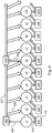
- FIG. 4 depicts a schematic overview of overlay sampling and control of a semiconductor manufacturing process.
- a sequence of ten operations L1 to L10 of an exposure process step on ten wafer lots (or batches, or wafers) are shown.
- a value of a high-order overlay parameter HO1 is obtained based on measurements 404 of the first lot L1 using a spatially dense sampling scheme.
- the high-order overlay parameter HO1 is used to determine control recipes 406 of subsequent exposures L2 to L6 of the next five lots.
- an updated value of the high-order overlay parameter HO6 is obtained based on the earlier 402 high-order overlay parameter HO1 and based on measurements 408 of the sixth lot L6 using the spatially dense sampling scheme.
- the higher-order parameter update repeats at the exposure of every fifth lot.
- low-order corrections are calculated per lot from sparse measurements.
- a low-order overlay parameter LO1 is obtained based on measurements 410 using a sparse sampling scheme, which is less spatially dense and more frequent than the spatially dense sampling scheme.
- the low-order parameter LO1 is used to determine the control recipe 412 of the subsequent operation L2 of the exposure step, and so on.
- the low-order corrections are calculated per lot from sparse measurements, and high-order corrections are obtained from dense measurements once in several lots.
- FIG. 5 depicts a schematic overview of alignment sampling and control of a semiconductor manufacturing process.
- wafer lots L1 to L10 have an off-line alignment mark measurement step 502.
- the measurements 504 are performed by an off-line measurement tool, 506, which is optimized for off-line measurements with a high spatial sampling density.
- the measured high-order alignment parameter values 508 are stored HO1 to HO10 for each wafer lot L1 to L10. Then each high-order alignment parameter value is used to to determine a control recipe 512 of the operation of an exposure step 514 on the corresponding wafer lot L1 to L10.
- low-order corrections are calculated per lot from sparse measurements.
- a low-order alignment parameter 516 is obtained based on measurements using a sparse sampling scheme, which is less spatially dense than the spatially dense sampling scheme. It has the same frequency (per lot) as the offline dense measurements 504 of the high-order alignment parameters.
- the low-order parameter 516 is used to determine the control recipe of the operation L1 of the same exposure step.
- Embodiments use a strategy for updating both overlay and alignment measurements in-between dense measurements using a Long Short-Term Memory (LSTM) prediction algorithm. This improves the performance of alignment and overlay control with minimum impact on throughput.
- LSTM Long Short-Term Memory
- a completely independent LSTM network prediction no dense measurement required after training is also possible, however it may diverge after some time if the learning becomes inadequate.
- Figure 6 depicts a schematic overview of a method of sampling and control of a semiconductor manufacturing process in accordance with an embodiment of the present invention.
- the neural network is configured with an initial training (TRN) step 602.
- Figure 6 depicts a method for predicting a value of a high-order parameter associated with a semiconductor manufacturing process.
- the semiconductor manufacturing processes a lithographic exposure process.
- the parameter is the third-order scanner exposure magnification parameter in the y-direction, D3y.
- the method involves obtaining a value 608 of the high-order parameter based on measurements 606 using a spatially dense sampling scheme.
- a recurrent neural network (NN) 604 is used to determine a predicted value 612 of the high-order parameter based on the measured value 608.
- the measured value 608 of the high-order parameter can be used directly 610 to determine the control recipe for processing of the measured lot.
- the predicted value 612 of the high-order parameter is determined based on the value 608 of the high-order parameter obtained from measurements 606 at a first operation L1 of a process step in the semiconductor manufacturing process to determine a control recipe 614 of a subsequent operation L2 of the process step in the semiconductor manufacturing process.
- a subsequent value 626 of the high-order parameter is obtained based on measurements 628 using the dense sampling scheme.
- a value 618 of a low-order parameter is obtained based on measurements (for example value 620 from measurements of lot at exposure step L2) using a spatially sparse sampling scheme.
- the sparse sampling scheme is less spatially dense and more frequent than the high-order sampling scheme used for measurements 606, 628.
- the value 620 of the low-order parameter is used to determine the control recipe 622 of the subsequent operation L2 of the exposure process step.
- the value 620 of the low-order parameter may be obtained based on measurements performed on the same substrate supported on the same substrate table at which the subsequent operation L2 of the process step is performed.
- the control recipe 622 is determined using the value 620 of the low-order parameter.
- the semiconductor manufacturing process is a batch-wise process of patterning substrates.
- the sampling scheme for obtaining high-order parameters has a measurement frequency of per 5 (as shown in Figure 6) to 10 batches.
- the second sampling scheme has a measurement frequency of one per batch.
- the semiconductor manufacturing process is a process of patterning substrates using exposure fields.
- the sampling scheme for obtaining high-order parameters has a spatial density of 200 to 300 measurement points per field and the sampling scheme for obtaining low-order parameters has a spatial density of 2 to 3 measurement points per field.
- the method of predicting a value of a parameter associated with the semiconductor manufacturing process may be implemented within a semiconductor manufacturing process.
- the method may be implemented in a lithographic apparatus with processing unit, such a LACU in Figure 2 . It may be implemented in a processor in the supervisory control system SCS of Figure 2 or computer system CL of Figure 3 .
- the invention may also be embodied as a computer program product comprising machine readable instructions for causing a general-purpose data processing apparatus to perform the steps of a method as described with reference to Figure 6 .
- Figure 7 is a graph of an overlay higher-order parameter update corresponding to the sampling and control scheme of Figure 4 .
- the horizontal axis is wafer number WN.
- the vertical axis is the third-order scanner exposure magnification parameter in the y-direction D3y.
- the solid line graph 702 is the original value of the high-order parameter from dense measurement sampling.
- the dashed line graph 704 to the right of the vertical dot-dash line is the higher-order parameter update with the parameter being updated every 10 points (note that Figure 4 shows this update every 5 points).
- Figure 8 is a graph of an overlay higher-order parameter update with no updates in accordance with an embodiment of the present invention.
- the dashed line graph 804 to the right of the vertical dot-dash line is the predicted parameter value with no updates. This would correspond to Figure 6 , but without an update at L6 or subsequently. Thus it uses a free LSTM, with no updates after training.
- Figure 9 is a graph of an overlay higher-order parameter update with updates corresponding to the sampling and control scheme of Figure 6 in accordance with an embodiment of the present invention.
- the dashed line graph 904 to the right of the vertical dot-dash line is the predicted parameter value with updates every 10 points (note that Figure 6 shows this update every 5 points).
- the LSTM network is trained with 78% of the data, to the left of the vertical dot-dash line.
- the LSTM network is validated on the rest (22% - 35 wafers, dashed line 904).
- Figure 10 depicts wafer maps of measured overlay with no high-order overlay parameter correction, with overlay higher-order parameter update corresponding to Figure 7 , and with overlay parameter prediction corresponding to Figures 8 and 9 .
- the real corrections are applied on dense (13*19 points per field) layout and the correction capability for each case is compared.
- the plots show mean plus 3 sigma overlay. A darker pattern represents worse overlay performance.
- a baseline wafer map 1002 is shown with no high-order correction.
- the wafer map 1004 results from overlay higher-order parameter update corresponding to the plot of Figure 7 , for conventional overlay.
- the wafer map 1006 results from overlay higher-order parameter update corresponding to the plot of Figure 8 , for a free LSTM with no updates.
- the wafer map 1008 results from overlay higher-order parameter update corresponding to the plot of Figure 9 , which is for LSTM prediction with updates. The latter has the best overlay correction performance, shown by the lighter pattern.
- Embodiments provide a way to include high-order parameters into alignment correction without measuring each wafer. Embodiments also improve the methodology for updating overlay measurements.
- lithographic apparatus in the manufacture of ICs, it should be understood that the lithographic apparatus described herein may have other applications. Possible other applications include the manufacture of integrated optical systems, guidance and detection patterns for magnetic domain memories, flat-panel displays, liquid-crystal displays (LCDs), thin-film magnetic heads, etc.
- Embodiments of the invention may form part of a mask inspection apparatus, a lithographic apparatus, or any apparatus that measures or processes an object such as a wafer (or other substrate) or mask (or other patterning device).
- the term metrology apparatus or metrology system encompasses or may be substituted with the term inspection apparatus or inspection system.
- a metrology or inspection apparatus as disclosed herein may be used to detect defects on or within a substrate and/or defects of structures on a substrate.
- a characteristic of the structure on the substrate may relate to defects in the structure, the absence of a specific part of the structure, or the presence of an unwanted structure on the substrate, for example.
- the inspection or metrology apparatus that comprises an embodiment of the invention may be used to determine characteristics of physical systems such as structures on a substrate or on a wafer.
- the inspection apparatus or metrology apparatus that comprises an embodiment of the invention may be used to detect defects of a substrate or defects of structures on a substrate or on a wafer.
- a characteristic of a physical structure may relate to defects in the structure, the absence of a specific part of the structure, or the presence of an unwanted structure on the substrate or on the wafer.
- targets or target structures are metrology target structures specifically designed and formed for the purposes of measurement
- properties of interest may be measured on one or more structures which are functional parts of devices formed on the substrate.
- Many devices have regular, grating-like structures.
- the terms structure, target grating and target structure as used herein do not require that the structure has been provided specifically for the measurement being performed.
- the different product features may comprise many regions with varying sensitivities (varying pitch etc.).
- pitch p of the metrology targets is close to the resolution limit of the optical system of the scatterometer, but may be much larger than the dimension of typical product features made by lithographic process in the target portions C.
- the lines and/or spaces of the overlay gratings within the target structures may be made to include smaller structures similar in dimension to the product features.
Landscapes
- Engineering & Computer Science (AREA)
- General Physics & Mathematics (AREA)
- Physics & Mathematics (AREA)
- Manufacturing & Machinery (AREA)
- Artificial Intelligence (AREA)
- Microelectronics & Electronic Packaging (AREA)
- Automation & Control Theory (AREA)
- Computer Hardware Design (AREA)
- Evolutionary Computation (AREA)
- Power Engineering (AREA)
- Computer Vision & Pattern Recognition (AREA)
- Medical Informatics (AREA)
- Software Systems (AREA)
- Health & Medical Sciences (AREA)
- General Engineering & Computer Science (AREA)
- Quality & Reliability (AREA)
- Exposure And Positioning Against Photoresist Photosensitive Materials (AREA)
Priority Applications (16)
| Application Number | Priority Date | Filing Date | Title |
|---|---|---|---|
| EP18204882.7A EP3650939A1 (fr) | 2018-11-07 | 2018-11-07 | Prédiction d'une valeur d'un paramètre de processus de fabrication de semiconducteurs |
| KR1020217013667A KR20210069104A (ko) | 2018-11-07 | 2019-10-09 | 공정에 대한 보정 결정 |
| JP2021524168A JP7280356B2 (ja) | 2018-11-07 | 2019-10-09 | プロセスに対する補正の決定 |
| CN201980073186.4A CN112969967A (zh) | 2018-11-07 | 2019-10-09 | 确定对过程的校正 |
| EP21197330.0A EP3974906A1 (fr) | 2018-11-07 | 2019-10-09 | Détermination d'une correction de procédé |
| PCT/EP2019/077353 WO2020094325A1 (fr) | 2018-11-07 | 2019-10-09 | Détermination de correction de processus |
| KR1020237029798A KR20230130767A (ko) | 2018-11-07 | 2019-10-09 | 공정에 대한 보정 결정 |
| EP19786562.9A EP3807720B1 (fr) | 2018-11-07 | 2019-10-09 | Procédé de configuration d'un processus de fabrication de semiconducteurs, appareil lithographique et produit de programme d'ordinateur associé |
| TW110119354A TWI777585B (zh) | 2018-11-07 | 2019-10-31 | 判定程序之校正 |
| TW108139392A TWI703659B (zh) | 2018-11-07 | 2019-10-31 | 判定程序之校正 |
| TW111134065A TWI824707B (zh) | 2018-11-07 | 2019-10-31 | 判定程序之校正 |
| TW109128463A TWI729918B (zh) | 2018-11-07 | 2019-10-31 | 判定程序之校正 |
| US17/174,159 US11086305B2 (en) | 2018-11-07 | 2021-02-11 | Determining a correction to a process |
| IL282101A IL282101B2 (en) | 2018-11-07 | 2021-04-06 | Methods for configuring a semiconductor manufacturing process |
| US17/367,901 US11994845B2 (en) | 2018-11-07 | 2021-07-06 | Determining a correction to a process |
| JP2023077714A JP2023095988A (ja) | 2018-11-07 | 2023-05-10 | プロセスに対する補正の決定 |
Applications Claiming Priority (1)
| Application Number | Priority Date | Filing Date | Title |
|---|---|---|---|
| EP18204882.7A EP3650939A1 (fr) | 2018-11-07 | 2018-11-07 | Prédiction d'une valeur d'un paramètre de processus de fabrication de semiconducteurs |
Publications (1)
| Publication Number | Publication Date |
|---|---|
| EP3650939A1 true EP3650939A1 (fr) | 2020-05-13 |
Family
ID=64183941
Family Applications (1)
| Application Number | Title | Priority Date | Filing Date |
|---|---|---|---|
| EP18204882.7A Withdrawn EP3650939A1 (fr) | 2018-11-07 | 2018-11-07 | Prédiction d'une valeur d'un paramètre de processus de fabrication de semiconducteurs |
Country Status (1)
| Country | Link |
|---|---|
| EP (1) | EP3650939A1 (fr) |
Cited By (3)
| Publication number | Priority date | Publication date | Assignee | Title |
|---|---|---|---|---|
| EP3951526A1 (fr) * | 2020-08-07 | 2022-02-09 | AT & S Austria Technologie & Systemtechnik Aktiengesellschaft | Détermination basée sur l'ai de plan d'action pour la fabrication de supports de composants |
| WO2022233562A1 (fr) | 2021-05-06 | 2022-11-10 | Asml Netherlands B.V. | Réseau neuronal convolutif causal pour une commande de processus |
| EP4105719A1 (fr) | 2021-06-15 | 2022-12-21 | ASML Netherlands B.V. | Réseau de convolution causal pour commande de processus |
Citations (4)
| Publication number | Priority date | Publication date | Assignee | Title |
|---|---|---|---|---|
| US6952253B2 (en) | 2002-11-12 | 2005-10-04 | Asml Netherlands B.V. | Lithographic apparatus and device manufacturing method |
| US20090063378A1 (en) * | 2007-08-31 | 2009-03-05 | Kla-Tencor Technologies Corporation | Apparatus and methods for predicting a semiconductor parameter across an area of a wafer |
| US20100049680A1 (en) * | 2008-08-20 | 2010-02-25 | Inotera Memories, Inc. | Method for projecting wafer product overlay error and wafer product critical dimension |
| US20170200265A1 (en) * | 2016-01-11 | 2017-07-13 | Kla-Tencor Corporation | Generating simulated output for a specimen |
-
2018
- 2018-11-07 EP EP18204882.7A patent/EP3650939A1/fr not_active Withdrawn
Patent Citations (4)
| Publication number | Priority date | Publication date | Assignee | Title |
|---|---|---|---|---|
| US6952253B2 (en) | 2002-11-12 | 2005-10-04 | Asml Netherlands B.V. | Lithographic apparatus and device manufacturing method |
| US20090063378A1 (en) * | 2007-08-31 | 2009-03-05 | Kla-Tencor Technologies Corporation | Apparatus and methods for predicting a semiconductor parameter across an area of a wafer |
| US20100049680A1 (en) * | 2008-08-20 | 2010-02-25 | Inotera Memories, Inc. | Method for projecting wafer product overlay error and wafer product critical dimension |
| US20170200265A1 (en) * | 2016-01-11 | 2017-07-13 | Kla-Tencor Corporation | Generating simulated output for a specimen |
Non-Patent Citations (3)
| Title |
|---|
| TUNG-HO LIN ET AL: "A novel key-variable sifting algorithm for virtual metrology", 2008 IEEE INTERNATIONAL CONFERENCE ON ROBOTICS AND AUTOMATION. THE HALF-DAY WORKSHOP ON: TOWARDS AUTONOMOUS AGRICULTURE OF TOMORROW; PASADENA, CA, USA, MAY 19-23, 2008, IEEE, PISCATAWAY, NJ, USA, 19 May 2008 (2008-05-19), pages 3636 - 3641, XP031340712, ISBN: 978-1-4244-1646-2 * |
| WANG JUNLIANG ET AL: "Bilateral LSTM: A Two-Dimensional Long Short-Term Memory Model With Multiply Memory Units for Short-Term Cycle Time Forecasting in Re-entrant Manufacturing Systems", IEEE TRANSACTIONS ON INDUSTRIAL INFORMATICS, IEEE SERVICE CENTER, NEW YORK, NY, US, vol. 14, no. 2, 1 February 2018 (2018-02-01), pages 748 - 758, XP011676823, ISSN: 1551-3203, [retrieved on 20180202], DOI: 10.1109/TII.2017.2754641 * |
| YU-CHUAN SU ET AL: "Implementation Considerations of Various Virtual Metrology Algorithms", AUTOMATION SCIENCE AND ENGINEERING, 2007. CASE 2007. IEEE INTERNATIONA L CONFERENCE ON, IEEE, PI, 1 September 2007 (2007-09-01), pages 276 - 281, XP031141551, ISBN: 978-1-4244-1153-5 * |
Cited By (3)
| Publication number | Priority date | Publication date | Assignee | Title |
|---|---|---|---|---|
| EP3951526A1 (fr) * | 2020-08-07 | 2022-02-09 | AT & S Austria Technologie & Systemtechnik Aktiengesellschaft | Détermination basée sur l'ai de plan d'action pour la fabrication de supports de composants |
| WO2022233562A1 (fr) | 2021-05-06 | 2022-11-10 | Asml Netherlands B.V. | Réseau neuronal convolutif causal pour une commande de processus |
| EP4105719A1 (fr) | 2021-06-15 | 2022-12-21 | ASML Netherlands B.V. | Réseau de convolution causal pour commande de processus |
Similar Documents
| Publication | Publication Date | Title |
|---|---|---|
| EP3807720B1 (fr) | Procédé de configuration d'un processus de fabrication de semiconducteurs, appareil lithographique et produit de programme d'ordinateur associé | |
| EP3650939A1 (fr) | Prédiction d'une valeur d'un paramètre de processus de fabrication de semiconducteurs | |
| US20220236647A1 (en) | Method for controlling a semiconductor manufacturing process | |
| US11809088B2 (en) | Method for controlling a lithographic apparatus | |
| EP3913435A1 (fr) | Configuration d'un modèle imputer | |
| US20220050391A1 (en) | Methods and apparatus for estimating substrate shape | |
| WO2021213746A1 (fr) | Configuration d'un modèle d'imputation | |
| US11994845B2 (en) | Determining a correction to a process | |
| EP4105719A1 (fr) | Réseau de convolution causal pour commande de processus | |
| US20230168594A1 (en) | Method of wafer alignment using at resolution metrology on product features | |
| CN114207527B (zh) | 用于控制半导体制造过程的方法 | |
| EP3848757A1 (fr) | Procédé de commande d'un appareil lithographique | |
| EP3839630A1 (fr) | Procédés et appareil pour configurer une demande de modèle de lentille | |
| EP3786711A1 (fr) | Erreur non corrigible en métrologie | |
| EP3650941A1 (fr) | Procédé de détermination de la contribution d'un appareil de traitement à un paramètre de substrat | |
| WO2021001119A1 (fr) | Erreur non corrigible en métrologie | |
| EP4244675A1 (fr) | Procédés et programmes informatiques pour la configuration d'un modèle de génération de schéma d'échantillonnage | |
| WO2020178003A1 (fr) | Procédé d'alignement et dispositif de mesure associé | |
| NL2024657A (en) | Method for controlling a lithographic apparatus |
Legal Events
| Date | Code | Title | Description |
|---|---|---|---|
| PUAI | Public reference made under article 153(3) epc to a published international application that has entered the european phase |
Free format text: ORIGINAL CODE: 0009012 |
|
| STAA | Information on the status of an ep patent application or granted ep patent |
Free format text: STATUS: THE APPLICATION HAS BEEN PUBLISHED |
|
| AK | Designated contracting states |
Kind code of ref document: A1 Designated state(s): AL AT BE BG CH CY CZ DE DK EE ES FI FR GB GR HR HU IE IS IT LI LT LU LV MC MK MT NL NO PL PT RO RS SE SI SK SM TR |
|
| AX | Request for extension of the european patent |
Extension state: BA ME |
|
| STAA | Information on the status of an ep patent application or granted ep patent |
Free format text: STATUS: THE APPLICATION IS DEEMED TO BE WITHDRAWN |
|
| 18D | Application deemed to be withdrawn |
Effective date: 20201114 |