EP3648555A1 - Method for manufacturing ceramic-metal layer assembly, method for manufacturing ceramic circuit board, and metal plate-joined ceramic base material plate - Google Patents
Method for manufacturing ceramic-metal layer assembly, method for manufacturing ceramic circuit board, and metal plate-joined ceramic base material plate Download PDFInfo
- Publication number
- EP3648555A1 EP3648555A1 EP18823451.2A EP18823451A EP3648555A1 EP 3648555 A1 EP3648555 A1 EP 3648555A1 EP 18823451 A EP18823451 A EP 18823451A EP 3648555 A1 EP3648555 A1 EP 3648555A1
- Authority
- EP
- European Patent Office
- Prior art keywords
- base material
- ceramic base
- material board
- ceramic
- scribe lines
- Prior art date
- Legal status (The legal status is an assumption and is not a legal conclusion. Google has not performed a legal analysis and makes no representation as to the accuracy of the status listed.)
- Withdrawn
Links
Images



Classifications
-
- H—ELECTRICITY
- H05—ELECTRIC TECHNIQUES NOT OTHERWISE PROVIDED FOR
- H05K—PRINTED CIRCUITS; CASINGS OR CONSTRUCTIONAL DETAILS OF ELECTRIC APPARATUS; MANUFACTURE OF ASSEMBLAGES OF ELECTRICAL COMPONENTS
- H05K3/00—Apparatus or processes for manufacturing printed circuits
- H05K3/0011—Working of insulating substrates or insulating layers
- H05K3/0044—Mechanical working of the substrate, e.g. drilling or punching
- H05K3/0052—Depaneling, i.e. dividing a panel into circuit boards; Working of the edges of circuit boards
-
- H—ELECTRICITY
- H05—ELECTRIC TECHNIQUES NOT OTHERWISE PROVIDED FOR
- H05K—PRINTED CIRCUITS; CASINGS OR CONSTRUCTIONAL DETAILS OF ELECTRIC APPARATUS; MANUFACTURE OF ASSEMBLAGES OF ELECTRICAL COMPONENTS
- H05K1/00—Printed circuits
- H05K1/02—Details
- H05K1/03—Use of materials for the substrate
- H05K1/0306—Inorganic insulating substrates, e.g. ceramic, glass
-
- B—PERFORMING OPERATIONS; TRANSPORTING
- B23—MACHINE TOOLS; METAL-WORKING NOT OTHERWISE PROVIDED FOR
- B23K—SOLDERING OR UNSOLDERING; WELDING; CLADDING OR PLATING BY SOLDERING OR WELDING; CUTTING BY APPLYING HEAT LOCALLY, e.g. FLAME CUTTING; WORKING BY LASER BEAM
- B23K1/00—Soldering, e.g. brazing, or unsoldering
- B23K1/0008—Soldering, e.g. brazing, or unsoldering specially adapted for particular articles or work
- B23K1/0016—Soldering of electronic components
-
- B—PERFORMING OPERATIONS; TRANSPORTING
- B23—MACHINE TOOLS; METAL-WORKING NOT OTHERWISE PROVIDED FOR
- B23K—SOLDERING OR UNSOLDERING; WELDING; CLADDING OR PLATING BY SOLDERING OR WELDING; CUTTING BY APPLYING HEAT LOCALLY, e.g. FLAME CUTTING; WORKING BY LASER BEAM
- B23K1/00—Soldering, e.g. brazing, or unsoldering
- B23K1/008—Soldering within a furnace
-
- B—PERFORMING OPERATIONS; TRANSPORTING
- B23—MACHINE TOOLS; METAL-WORKING NOT OTHERWISE PROVIDED FOR
- B23K—SOLDERING OR UNSOLDERING; WELDING; CLADDING OR PLATING BY SOLDERING OR WELDING; CUTTING BY APPLYING HEAT LOCALLY, e.g. FLAME CUTTING; WORKING BY LASER BEAM
- B23K1/00—Soldering, e.g. brazing, or unsoldering
- B23K1/19—Soldering, e.g. brazing, or unsoldering taking account of the properties of the materials to be soldered
-
- B—PERFORMING OPERATIONS; TRANSPORTING
- B23—MACHINE TOOLS; METAL-WORKING NOT OTHERWISE PROVIDED FOR
- B23K—SOLDERING OR UNSOLDERING; WELDING; CLADDING OR PLATING BY SOLDERING OR WELDING; CUTTING BY APPLYING HEAT LOCALLY, e.g. FLAME CUTTING; WORKING BY LASER BEAM
- B23K1/00—Soldering, e.g. brazing, or unsoldering
- B23K1/20—Preliminary treatment of work or areas to be soldered, e.g. in respect of a galvanic coating
-
- B—PERFORMING OPERATIONS; TRANSPORTING
- B23—MACHINE TOOLS; METAL-WORKING NOT OTHERWISE PROVIDED FOR
- B23K—SOLDERING OR UNSOLDERING; WELDING; CLADDING OR PLATING BY SOLDERING OR WELDING; CUTTING BY APPLYING HEAT LOCALLY, e.g. FLAME CUTTING; WORKING BY LASER BEAM
- B23K26/00—Working by laser beam, e.g. welding, cutting or boring
- B23K26/36—Removing material
- B23K26/362—Laser etching
- B23K26/364—Laser etching for making a groove or trench, e.g. for scribing a break initiation groove
-
- B—PERFORMING OPERATIONS; TRANSPORTING
- B23—MACHINE TOOLS; METAL-WORKING NOT OTHERWISE PROVIDED FOR
- B23K—SOLDERING OR UNSOLDERING; WELDING; CLADDING OR PLATING BY SOLDERING OR WELDING; CUTTING BY APPLYING HEAT LOCALLY, e.g. FLAME CUTTING; WORKING BY LASER BEAM
- B23K26/00—Working by laser beam, e.g. welding, cutting or boring
- B23K26/36—Removing material
- B23K26/40—Removing material taking account of the properties of the material involved
- B23K26/402—Removing material taking account of the properties of the material involved involving non-metallic material, e.g. isolators
-
- C—CHEMISTRY; METALLURGY
- C04—CEMENTS; CONCRETE; ARTIFICIAL STONE; CERAMICS; REFRACTORIES
- C04B—LIME, MAGNESIA; SLAG; CEMENTS; COMPOSITIONS THEREOF, e.g. MORTARS, CONCRETE OR LIKE BUILDING MATERIALS; ARTIFICIAL STONE; CERAMICS; REFRACTORIES; TREATMENT OF NATURAL STONE
- C04B35/00—Shaped ceramic products characterised by their composition; Ceramics compositions; Processing powders of inorganic compounds preparatory to the manufacturing of ceramic products
- C04B35/622—Forming processes; Processing powders of inorganic compounds preparatory to the manufacturing of ceramic products
- C04B35/64—Burning or sintering processes
- C04B35/645—Pressure sintering
-
- C—CHEMISTRY; METALLURGY
- C04—CEMENTS; CONCRETE; ARTIFICIAL STONE; CERAMICS; REFRACTORIES
- C04B—LIME, MAGNESIA; SLAG; CEMENTS; COMPOSITIONS THEREOF, e.g. MORTARS, CONCRETE OR LIKE BUILDING MATERIALS; ARTIFICIAL STONE; CERAMICS; REFRACTORIES; TREATMENT OF NATURAL STONE
- C04B37/00—Joining burned ceramic articles with other burned ceramic articles or other articles by heating
- C04B37/02—Joining burned ceramic articles with other burned ceramic articles or other articles by heating with metallic articles
- C04B37/023—Joining burned ceramic articles with other burned ceramic articles or other articles by heating with metallic articles characterised by the interlayer used
- C04B37/026—Joining burned ceramic articles with other burned ceramic articles or other articles by heating with metallic articles characterised by the interlayer used consisting of metals or metal salts
-
- H—ELECTRICITY
- H05—ELECTRIC TECHNIQUES NOT OTHERWISE PROVIDED FOR
- H05K—PRINTED CIRCUITS; CASINGS OR CONSTRUCTIONAL DETAILS OF ELECTRIC APPARATUS; MANUFACTURE OF ASSEMBLAGES OF ELECTRICAL COMPONENTS
- H05K3/00—Apparatus or processes for manufacturing printed circuits
- H05K3/0011—Working of insulating substrates or insulating layers
- H05K3/0017—Etching of the substrate by chemical or physical means
-
- H—ELECTRICITY
- H05—ELECTRIC TECHNIQUES NOT OTHERWISE PROVIDED FOR
- H05K—PRINTED CIRCUITS; CASINGS OR CONSTRUCTIONAL DETAILS OF ELECTRIC APPARATUS; MANUFACTURE OF ASSEMBLAGES OF ELECTRICAL COMPONENTS
- H05K3/00—Apparatus or processes for manufacturing printed circuits
- H05K3/0058—Laminating printed circuit boards onto other substrates, e.g. metallic substrates
- H05K3/0061—Laminating printed circuit boards onto other substrates, e.g. metallic substrates onto a metallic substrate, e.g. a heat sink
-
- H—ELECTRICITY
- H05—ELECTRIC TECHNIQUES NOT OTHERWISE PROVIDED FOR
- H05K—PRINTED CIRCUITS; CASINGS OR CONSTRUCTIONAL DETAILS OF ELECTRIC APPARATUS; MANUFACTURE OF ASSEMBLAGES OF ELECTRICAL COMPONENTS
- H05K3/00—Apparatus or processes for manufacturing printed circuits
- H05K3/02—Apparatus or processes for manufacturing printed circuits in which the conductive material is applied to the surface of the insulating support and is thereafter removed from such areas of the surface which are not intended for current conducting or shielding
- H05K3/06—Apparatus or processes for manufacturing printed circuits in which the conductive material is applied to the surface of the insulating support and is thereafter removed from such areas of the surface which are not intended for current conducting or shielding the conductive material being removed chemically or electrolytically, e.g. by photo-etch process
-
- H—ELECTRICITY
- H10—SEMICONDUCTOR DEVICES; ELECTRIC SOLID-STATE DEVICES NOT OTHERWISE PROVIDED FOR
- H10W—GENERIC PACKAGES, INTERCONNECTIONS, CONNECTORS OR OTHER CONSTRUCTIONAL DETAILS OF DEVICES COVERED BY CLASS H10
- H10W40/00—Arrangements for thermal protection or thermal control
- H10W40/20—Arrangements for cooling
- H10W40/25—Arrangements for cooling characterised by their materials
- H10W40/255—Arrangements for cooling characterised by their materials having a laminate or multilayered structure, e.g. direct bond copper [DBC] ceramic substrates
-
- H—ELECTRICITY
- H10—SEMICONDUCTOR DEVICES; ELECTRIC SOLID-STATE DEVICES NOT OTHERWISE PROVIDED FOR
- H10W—GENERIC PACKAGES, INTERCONNECTIONS, CONNECTORS OR OTHER CONSTRUCTIONAL DETAILS OF DEVICES COVERED BY CLASS H10
- H10W99/00—Subject matter not provided for in other groups of this subclass
-
- B—PERFORMING OPERATIONS; TRANSPORTING
- B23—MACHINE TOOLS; METAL-WORKING NOT OTHERWISE PROVIDED FOR
- B23K—SOLDERING OR UNSOLDERING; WELDING; CLADDING OR PLATING BY SOLDERING OR WELDING; CUTTING BY APPLYING HEAT LOCALLY, e.g. FLAME CUTTING; WORKING BY LASER BEAM
- B23K2101/00—Articles made by soldering, welding or cutting
- B23K2101/36—Electric or electronic devices
- B23K2101/42—Printed circuits
-
- B—PERFORMING OPERATIONS; TRANSPORTING
- B23—MACHINE TOOLS; METAL-WORKING NOT OTHERWISE PROVIDED FOR
- B23K—SOLDERING OR UNSOLDERING; WELDING; CLADDING OR PLATING BY SOLDERING OR WELDING; CUTTING BY APPLYING HEAT LOCALLY, e.g. FLAME CUTTING; WORKING BY LASER BEAM
- B23K2103/00—Materials to be soldered, welded or cut
- B23K2103/08—Non-ferrous metals or alloys
- B23K2103/10—Aluminium or alloys thereof
-
- B—PERFORMING OPERATIONS; TRANSPORTING
- B23—MACHINE TOOLS; METAL-WORKING NOT OTHERWISE PROVIDED FOR
- B23K—SOLDERING OR UNSOLDERING; WELDING; CLADDING OR PLATING BY SOLDERING OR WELDING; CUTTING BY APPLYING HEAT LOCALLY, e.g. FLAME CUTTING; WORKING BY LASER BEAM
- B23K2103/00—Materials to be soldered, welded or cut
- B23K2103/18—Dissimilar materials
-
- B—PERFORMING OPERATIONS; TRANSPORTING
- B23—MACHINE TOOLS; METAL-WORKING NOT OTHERWISE PROVIDED FOR
- B23K—SOLDERING OR UNSOLDERING; WELDING; CLADDING OR PLATING BY SOLDERING OR WELDING; CUTTING BY APPLYING HEAT LOCALLY, e.g. FLAME CUTTING; WORKING BY LASER BEAM
- B23K2103/00—Materials to be soldered, welded or cut
- B23K2103/50—Inorganic materials other than metals or composite materials
- B23K2103/52—Ceramics
-
- C—CHEMISTRY; METALLURGY
- C04—CEMENTS; CONCRETE; ARTIFICIAL STONE; CERAMICS; REFRACTORIES
- C04B—LIME, MAGNESIA; SLAG; CEMENTS; COMPOSITIONS THEREOF, e.g. MORTARS, CONCRETE OR LIKE BUILDING MATERIALS; ARTIFICIAL STONE; CERAMICS; REFRACTORIES; TREATMENT OF NATURAL STONE
- C04B2237/00—Aspects relating to ceramic laminates or to joining of ceramic articles with other articles by heating
- C04B2237/02—Aspects relating to interlayers, e.g. used to join ceramic articles with other articles by heating
- C04B2237/12—Metallic interlayers
- C04B2237/121—Metallic interlayers based on aluminium
-
- C—CHEMISTRY; METALLURGY
- C04—CEMENTS; CONCRETE; ARTIFICIAL STONE; CERAMICS; REFRACTORIES
- C04B—LIME, MAGNESIA; SLAG; CEMENTS; COMPOSITIONS THEREOF, e.g. MORTARS, CONCRETE OR LIKE BUILDING MATERIALS; ARTIFICIAL STONE; CERAMICS; REFRACTORIES; TREATMENT OF NATURAL STONE
- C04B2237/00—Aspects relating to ceramic laminates or to joining of ceramic articles with other articles by heating
- C04B2237/02—Aspects relating to interlayers, e.g. used to join ceramic articles with other articles by heating
- C04B2237/12—Metallic interlayers
- C04B2237/126—Metallic interlayers wherein the active component for bonding is not the largest fraction of the interlayer
- C04B2237/128—The active component for bonding being silicon
-
- C—CHEMISTRY; METALLURGY
- C04—CEMENTS; CONCRETE; ARTIFICIAL STONE; CERAMICS; REFRACTORIES
- C04B—LIME, MAGNESIA; SLAG; CEMENTS; COMPOSITIONS THEREOF, e.g. MORTARS, CONCRETE OR LIKE BUILDING MATERIALS; ARTIFICIAL STONE; CERAMICS; REFRACTORIES; TREATMENT OF NATURAL STONE
- C04B2237/00—Aspects relating to ceramic laminates or to joining of ceramic articles with other articles by heating
- C04B2237/30—Composition of layers of ceramic laminates or of ceramic or metallic articles to be joined by heating, e.g. Si substrates
- C04B2237/40—Metallic
- C04B2237/402—Aluminium
-
- C—CHEMISTRY; METALLURGY
- C04—CEMENTS; CONCRETE; ARTIFICIAL STONE; CERAMICS; REFRACTORIES
- C04B—LIME, MAGNESIA; SLAG; CEMENTS; COMPOSITIONS THEREOF, e.g. MORTARS, CONCRETE OR LIKE BUILDING MATERIALS; ARTIFICIAL STONE; CERAMICS; REFRACTORIES; TREATMENT OF NATURAL STONE
- C04B2237/00—Aspects relating to ceramic laminates or to joining of ceramic articles with other articles by heating
- C04B2237/50—Processing aspects relating to ceramic laminates or to the joining of ceramic articles with other articles by heating
- C04B2237/64—Forming laminates or joined articles comprising grooves or cuts
-
- C—CHEMISTRY; METALLURGY
- C04—CEMENTS; CONCRETE; ARTIFICIAL STONE; CERAMICS; REFRACTORIES
- C04B—LIME, MAGNESIA; SLAG; CEMENTS; COMPOSITIONS THEREOF, e.g. MORTARS, CONCRETE OR LIKE BUILDING MATERIALS; ARTIFICIAL STONE; CERAMICS; REFRACTORIES; TREATMENT OF NATURAL STONE
- C04B2237/00—Aspects relating to ceramic laminates or to joining of ceramic articles with other articles by heating
- C04B2237/50—Processing aspects relating to ceramic laminates or to the joining of ceramic articles with other articles by heating
- C04B2237/70—Forming laminates or joined articles comprising layers of a specific, unusual thickness
- C04B2237/706—Forming laminates or joined articles comprising layers of a specific, unusual thickness of one or more of the metallic layers or articles
-
- C—CHEMISTRY; METALLURGY
- C04—CEMENTS; CONCRETE; ARTIFICIAL STONE; CERAMICS; REFRACTORIES
- C04B—LIME, MAGNESIA; SLAG; CEMENTS; COMPOSITIONS THEREOF, e.g. MORTARS, CONCRETE OR LIKE BUILDING MATERIALS; ARTIFICIAL STONE; CERAMICS; REFRACTORIES; TREATMENT OF NATURAL STONE
- C04B2237/00—Aspects relating to ceramic laminates or to joining of ceramic articles with other articles by heating
- C04B2237/50—Processing aspects relating to ceramic laminates or to the joining of ceramic articles with other articles by heating
- C04B2237/70—Forming laminates or joined articles comprising layers of a specific, unusual thickness
- C04B2237/708—Forming laminates or joined articles comprising layers of a specific, unusual thickness of one or more of the interlayers
-
- H—ELECTRICITY
- H05—ELECTRIC TECHNIQUES NOT OTHERWISE PROVIDED FOR
- H05K—PRINTED CIRCUITS; CASINGS OR CONSTRUCTIONAL DETAILS OF ELECTRIC APPARATUS; MANUFACTURE OF ASSEMBLAGES OF ELECTRICAL COMPONENTS
- H05K2201/00—Indexing scheme relating to printed circuits covered by H05K1/00
- H05K2201/09—Shape and layout
- H05K2201/09009—Substrate related
- H05K2201/0909—Preformed cutting or breaking line
-
- H—ELECTRICITY
- H05—ELECTRIC TECHNIQUES NOT OTHERWISE PROVIDED FOR
- H05K—PRINTED CIRCUITS; CASINGS OR CONSTRUCTIONAL DETAILS OF ELECTRIC APPARATUS; MANUFACTURE OF ASSEMBLAGES OF ELECTRICAL COMPONENTS
- H05K2203/00—Indexing scheme relating to apparatus or processes for manufacturing printed circuits covered by H05K3/00
- H05K2203/15—Position of the PCB during processing
- H05K2203/1572—Processing both sides of a PCB by the same process; Providing a similar arrangement of components on both sides; Making interlayer connections from two sides
-
- H—ELECTRICITY
- H05—ELECTRIC TECHNIQUES NOT OTHERWISE PROVIDED FOR
- H05K—PRINTED CIRCUITS; CASINGS OR CONSTRUCTIONAL DETAILS OF ELECTRIC APPARATUS; MANUFACTURE OF ASSEMBLAGES OF ELECTRICAL COMPONENTS
- H05K3/00—Apparatus or processes for manufacturing printed circuits
- H05K3/0011—Working of insulating substrates or insulating layers
- H05K3/0017—Etching of the substrate by chemical or physical means
- H05K3/0026—Etching of the substrate by chemical or physical means by laser ablation
- H05K3/0029—Etching of the substrate by chemical or physical means by laser ablation of inorganic insulating material
Definitions
- the present invention is related to a method for manufacturing a ceramic-metal layer assembly in which the metal layers are joined on respective surfaces of a ceramic base material board, a method for manufacturing a ceramic circuit board by dividing the ceramic-metal layer assembly, and a metal-board-joined ceramic base material board in which metal boards are joined on both surfaces of the ceramic base material board.
- Patent Document 1 Japanese Unexamined Patent Application, First Publication No. 2015-185606
- the metal boards are laminated on both surfaces of the ceramic base material board with the brazing material therebetween, and this laminated assembly is heated in a pressurized state by being held between carbon boards: the brazing material is melted and spread between the ceramic base material board and the metal boards, and Si atoms in the brazing material are dispersed into the metal boards: as a result, the ceramic base material board and the metal boards are joined.
- the melted brazing material is flown out from the laminated assembly along the scribe lines, so that braze lumps are generated at ends of the scribe lines.
- the Si atoms are dispersed into the metal board at the back surface side with the larger number than that of the Si atoms in the brazing material dispersed into the metal board at the front surface side: content amount of the Si atoms are different.
- Etching rates of etching work after bonding the ceramic base material board and the metal boards are different between at the front and back surfaces: manufactured is a power module board having the metal layers with different areas between at the front and back surfaces.
- the metal board at the back surface side has the higher Si density and lower melting point, so it is easier to be melted than the metal board at the front surface side. Accordingly, a liquid phase is generated on a surface of the metal board at the back surface side by heating for bonding and it becomes braze stains: if it is remarkable, there is a problem in that the carbon board is adhered to the metal board at the back surface side.
- the present invention is achieved in consideration of the above circumstances, and has an object to reduce the difference of the Si density between the metal boards joined to the respective surfaces of the ceramic base material board, substantially equalize the etching rates of the respective metal boards, and reduce generation of the braze stain generated on the surfaces of the metal boards.
- the present invention is a method for manufacturing a ceramic-metal layer assembly having: a step of forming scribe lines, forming at least one scribe line respective on a front surface and a back surface of a ceramic base material board along dividing lines for dividing the ceramic base material board into a plurality of ceramic boards; a step of joining, laminating a metal board made of aluminum or aluminum alloy with a thickness dimension of not more than 0.4 mm respective on each of the front surface and the back surface of the ceramic base material board with Al-Si base brazing material therebetween so as to cover at least a part of the dividing lines, and heating with pressurizing in a laminating direction; so that the metal boards are joined respectively on the front surface and the back surface of the ceramic base material board; and a step of etching, forming a plurality of metal layers by etching the metal boards along the dividing lines: thereby manufactured is the ceramic-metal layer assembly in which the plurality of metal layers are joined respectively on the front surface and the back surface of the ceramic base material
- the scribe line is formed on only one surface of the ceramic base material board
- more Si atoms in the brazing material are dispersed in the metal board joined on the back surface on which the scribe lines are not formed than the Si atoms in the brazing material dispersed in the metal board joined on the front surface on which the scribe lines are formed.
- the melting point of the metal board on the back surface side is reduced, so that the braze stain may be generated.
- the present invention by forming the scribe lines on respective the front surface and the back surface of the ceramic base material board, when the metal boards are joined on both the surfaces of the ceramic base material board, it is possible to discharge surpluses of the melted brazing material to the outside of the laminated assembly along the scribe lines on both the surfaces. Accordingly, in comparing to a case in which the scribe lines are formed only on one surface, the difference of the content amount of the Si atoms (a difference of the Si density) dispersed from the brazing material is reduced between the metal boards on both the surfaces of the ceramic base material board: so that the metal boards can be etched at substantially the same etching rate, and it is possible to form the metal layers with substantially the same size.
- the scribe lines on both the surface of the ceramic base material board the surpluses of the melted brazing material on both the surfaces are smoothly discharged to the outside of the laminated assembly: as a result, it is possible to prevent the metal boards from generating a liquid phase because of falling of the melting point, and the braze stain on the surfaces of the metal boards can be suppressed.
- the plural scribe lines may be formed on respective the front surface and the back surface of the ceramic base material board.
- the brazing material melted in the step of joining is easy to be discharged because it is dispersed to the outside of the laminated assembly on both the front surface and the back surface, and the Si density in the metal boards can be uniform in a surface direction. Since the Si density is uniform in the surface direction, the difference of the content amount of the Si atoms dispersed from the brazing material into the metal boards at the front surface side and the back surface side is small: accordingly, the metal boards on both the surfaces can be etched at the same etching rate, and the metal layers can be formed with substantially the same size.
- the braze lumps can be suppressed from being larger.
- the scribe lines that are formed on the front surface of the ceramic base material board and the scribe lines that are formed on the back surface of the ceramic base material board be a same number.
- the amounts of the brazing material discharged outside the laminated assembly along the scribe lines are substantially the same on the front surface and the back surface in the step of joining.
- the content amount of the Si atoms i.e., the Si density dispersed in the metal boards joined on the front surface and the back surface are the same and the etching rate etching the metal boards are the same, so that the same size of the metal layers can be formed.
- the scribe lines on the front surface of the ceramic base material board and the scribe lines on the back surface of the ceramic base material board be formed at a same position in the surface direction of the ceramic base material board.
- the scribe lines By forming the scribe lines on the same position on both the face of the ceramic base material board, it is easy to split the ceramic base material board into pieces along the scribe lines, so that a plurality of ceramic circuit boards can be efficiently manufactured.
- the positions may be different between the scribe lines formed on the front surface of the ceramic base material board and the scribe lines formed on the back surface of the ceramic base material board in the surface direction of the ceramic base material board.
- the number of the scribe lines can be less than the number of the scribe lines which are formed on the same position on both the surfaces of the ceramic base material board, it is possible to reduce works and time for the step of forming scribe lines.
- a method for manufacturing a ceramic circuit board of the present invention further includes a step of dividing after the step of etching in the above-described method for manufacturing, dividing the ceramic base material board along the scribe lines into pieces of the ceramic boards, so that the ceramic circuit boards in which the metal layers are joined respectively on the front surface and the back surface of the ceramic boards are manufactured.
- a metal-board-joined ceramic base material board of the present invention is provided with: a ceramic base material board having at least one scribe line on each of a front surface and a back surface, in which the scribe lines are formed along dividing lines for dividing the ceramic base material board into a plurality of ceramic boards; and metal boards joined respectively on the front surface and the back surface of the ceramic base material board, in which the metal boards cover at least a part of dividing lines and are made of aluminum with a thickness dimension not more than 0.4 mm.
- a plurality of the scribe lines may be formed respectively on the front surface and the back surface of the ceramic base material board.
- the scribe lines formed on the front surface of the ceramic base material board and the scribe lines formed on the back surface of the ceramic base material board may be a same number.
- the scribe lines on the front surface of the ceramic base material board and the scribe line on the back surface of the ceramic base material board may be formed at a same position in the surface direction of the ceramic base material board.
- the scribe lines on the front surface of the ceramic base material board and the scribe line on the back surface of the ceramic base material board may be formed at different positions in the surface direction of the ceramic base material board.
- the etching rate can be substantially the same for both the metal boards; and the braze stain generated on the surfaces of the metal boards can be suppressed.
- FIG. 1 is a sectional view showing a ceramic circuit board 1 of a first embodiment.
- the ceramic circuit board 1 is used as a wiring board of a thermoelectric conversion element for instance, and provided with a ceramic board 2 formed in a rectangular shape having a vertical dimension of 5 mm and a horizontal dimension of 5 mm in a plan view and metal layers 3 and 4 that are joined on both surfaces of the ceramic board 2 .
- the ceramic board 2 is a material board made of a ceramic material such as aluminum nitride (AlN), silicon nitride (Si 3 N 4 ), alumina or the like with a thickness L1 (refer to FIG. 6 ) of 0.3 mm to 1.0 mm.
- AlN aluminum nitride
- Si 3 N 4 silicon nitride
- L1 thickness of 0.3 mm to 1.0 mm.
- the metal layers 3 and 4 are material boards made of pure aluminum of purity not less than 99.00% by mass, pure aluminum of purity not less than 99.99% by mass, or aluminum alloy of JIS3003 or the like with a thickness not more than 0.4 mm (e.g., 0.25 mm).
- the metal layers 3 and 4 and the ceramic board 2 are joined with brazing material of Al-Si base.
- scribe lines 21a are formed on a front surface 20a and scribe lines 21b are formed on a back surface 20b of the ceramic board 2 as shown in FIG. 3A and FIG. 4 (a step of forming scribe lines).
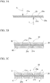
- metal boards 30 and 40 to be the metal layers 3 and 4 are joined on both the surfaces of the ceramic base material board 20 as shown in FIG. 3B (a step of joining), so that a metal-board-joined ceramic base material board (hereinafter, a first joined assembly) 50 is formed.
- the metal boards 30 and 40 of the first joined assembly 50 are etched along dividing lines (the scribe lines 21a and 21b) as shown in FIG. 3C (a step of etching), so that ceramic-metal layer assembly (hereinafter, a second joined assembly) 60 is manufactured.
- the ceramic base material board 20 is divided into pieces as shown in FIG. 3D (a step of dividing), so that the ceramic circuit board 1 are manufactured.
- step of forming scribe lines, the step of joining, the step of etching, the step of plating and the step of dividing which are carried out in order as shown in FIG. 2 will be explained in detail in order.
- the scribe lines 21a on the front surface 20a and the scribe lines 21b on the back surface 20b are formed along the dividing lines which divide the ceramic base material board 20 with a rectangular board shape into the multiple ceramic boards 2.
- the scribe lines 21a and 21b are groove parts formed on the ceramic base material board 20, formed by removing the front surface 20a and the back surface 20b of the ceramic base material board 20 linearly, by emitting laser light L(CO 2 laser, YAG laser, YVO 4 laser, YLF laser or the like) for instance.
- the scribe lines 21a and 21b are starting parts of dividing the ceramic base material board 20 in the step of dividing, formed on at least one of the front surface 20a or the back surface 20b of the ceramic base material board 20 along the dividing lines.
- FIG. 4 is a plan view of the ceramic base material board 20 on which the scribe lines 21a and 21b are formed by the step of forming scribe lines.
- FIG. 5 is a cross sectional arrow view showing a part of a cross section along the line A1-A1 shown in FIG. 4 .
- formed by the step of forming scribe lines on the front surface 20a of the ceramic base material board 20 are: the fifteen scribe lines 21a extending vertically, and substantially in parallel with a prescribed interval to each other, and the six scribe lines 21a extending laterally, and substantially in parallel with a prescribed interval to each other.
- the fourteen scribe lines 21b extending vertically, and substantially in parallel with a prescribed interval to each other, and the five scribe lines 21b extending laterally, and substantially in parallel with a prescribed interval to each other.
- the respective scribe lines 21b extending vertically on the back surface 20b are formed substantially in parallel to the scribe lines 21a extending vertically on the front surface 20a but on different positions from them; that is to say, formed between the scribe lines 21a on the front surface 20a.
- the respective scribe lines 21b extending laterally on the back surface 20b are formed substantially in parallel to the six scribe lines 21a extending laterally on the front surface 20a but on different positions from them; that is to say, formed between the scribe lines 21a on the front surface 20a.
- the interval between the respective scribe lines 21a on the front surface 20a and the interval between the respective scribe lines 21b on the back surface 20b of the ceramic base material board 20 are both 10 mm: the scribe lines 21a on the front surface 20a and the scribe lines 21b on the back surface 20b are disposed with being shifted by 5 mm to each other in a surface direction of the ceramic base material board 20. Accordingly, in a plan view of the ceramic base material board 20, the scribe lines 21a on the front surface 20a and the scribe lines 21b on the back surface 20b are disposed with a pitch 5 mm in the vertical direction and the lateral direction respectively.
- the 280 ceramic boards 2 are formed with 5 mm square in a plan view, by dividing the ceramic base material board 20 along the scribe lines 21a and 21b on the dividing lines in the step of dividing.
- a peripheral end part of the ceramic base material board 20 (parts between end edges of the ceramic base material board 20 and the outermost scribe lines 21a and 21b) are a margin part 20c, which is not used as the ceramic board 2 (refer to FIG. 4 ). Accordingly, although the dividing lines forming the outline of the ceramic board 2 are not set in the margin part 20c, the scribe lines 21a and 21b are formed to be extended into the margin part 20c, in order to divide the ceramic base material board 20 without breaking the ceramic board 2.
- FIG. 6 is a partly enlarged view of FIG. 5 .
- the scribe lines 21a and 21b are formed to have a depth dimension L2 and a maximum width dimension L3 respectively on the front surface 20a and the back surface 20b of the ceramic base material board 20 with a thickness dimension L1. Accordingly, a thickness dimension L4 of the ceramic base material board 20 along the dividing lines on which the scribe lines 21a and 21b are formed is smaller than the thickness L1 of the ceramic base material board 20 at a part on which the scribe lines 21a and 21b are not formed.
- the depth dimension L2 of the scribe lines 21a and 21b be 0.1 mm to 0.3 mm and the width dimension L3 be 0.05 mm to 0.2 mm.
- L1 is set to 0.635 mm
- L2 is set to 0.2 mm
- L3 is set to 0.1 mm
- L4 is set to 0.435 mm.
- the scribe lines 21a and 21b it is preferable to form the scribe lines 21a and 21b so that at least one end part thereof reach the end edge (the margin part 20c which is an outer part of the metal boards 30 and 40) of the ceramic base material board 20.
- the scribe lines 21a and 21b it is not possible to run the brazing material which is melted in the step of joining via the scribe lines to the outside.
- the scribe lines 21a and 21b are formed to reach both the end edges of the ceramic base material board 20.
- the ceramic base material board 20 is washed by washing solution but the illustration is omitted.
- the metal boards 30 and 40 (refer to FIG. 4 ) having a thickness not more than 0.4 mm and a size (substantially a same size as inside the margin part 20c in the present embodiment) covering at least a part of the scribe lines 21a and 21b (the dividing lines) in a plan view are joined on the ceramic base material board 20 which is washed after forming the scribe lines 21a and 21b using brazing material of Al-Si base.
- the metal boards 30 and 40 are layered on the front surface 20a and the back surface 20b of the ceramic base material board 20 respectively with foils of brazing material of Al-Si base therebetween; and a laminated assembly of these is held between carbon plates and pressurized in a laminate direction and heated in vacuum (in a state of pressurizing).
- the metal-board-joined ceramic base material board (the first joined assembly) 50 is formed (refer to FIG. 3B ) in which the metal boards 30 and 40 are joined on the front surface 20a and the back surface 20b of the ceramic base material board 20 respectively.
- the pressurizing force in the laminate direction be 0.1 MPa to 0.5 MPa and heating temperature be 630°C to 650°C.
- the foils of brazing material of Al-Si base have a thickness 5 ⁇ m to 15 ⁇ m.
- the heating temperature is lower than a melting point of the metal boards 30 and 40.
- Al-Si base brazing material Al-Si-Cu brazing material and Al-Si-Mg brazing material or the like can be used. It is desirable that Si density in the brazing material be 5% by mass to 12% by mass.
- the brazing material is melted when joining and flows out partly: the remainder is entirely or mostly used for brazing and dispersed into the metal boards 30 and 40. Accordingly, there is a case in which a slight brazing material layer remains between the ceramic base material board 20 and the metal boards 30 and 40 after joining, or a case of scarcely remains.
- the scribe lines 21a are formed on the front surface 20a with fifteen vertically and six laterally: and the scribe lines 21b are formed on the back surface 20b with fourteen vertically and five laterally. These numbers of the scribe lines 21a and 21b can be deemed to be substantially the same between the front surface 20a and the back surface 20b.
- quantities of the brazing material that flows outside the metal boards 30 and 40 along the scribe lines 21a and 21b in the step of joining are substantially the same quantity at both the surfaces of the ceramic base material board 20. Accordingly, the brazing material remains between the metal boards 30 and 40 and the ceramic base material board 20, and the quantities thereof are substantially the same on the front surface 20a and the back surface 20b. Thereby substantially the same amount of the Si atoms are dispersed into the metal boards 30 and 40 respectively, so that Si density in the metal boards 30 and 40 are substantially the same.
- the melted brazing material is discharged outside the laminated assembly along the scribe lines 21a and 21b, increase of the Si density resulting from remaining of the brazing material is suppressed, so that the melting point of the metal boards 30 and 40 is prevented from falling: as a result, braze stains on surfaces of the metal boards 30 and 40 are reduced.
- the metal boards 30 and 40 in the first joined assembly 50 are etched along the dividing lines (the scribe lines 21a and 21b). Etching can be carried out by known methods, for example, a method using iron chloride solution after masking necessary parts.
- the scribe lines 21a and 21b are exposed by etching and a plurality of the metal layers 3 and 4 are formed which are isolated from each other in a rectangular shape in a plan view, so that the metal-layer-joined ceramic base material board (the second joined assembly) 60 is formed (refer to FIG. 3C ).
- the metal board 30 joined on the front surface 20a and the metal board 40 joined on the back surface 20b of the ceramic base material board 20 have substantially the same etching rate since the Si density are the same; accordingly etching widths are also substantially the same.
- the second joined assembly 60 having the metal layers 3 and 4 with substantially the same size between the dividing lines is formed.
- plating treatment(s) such as gold plating, silver plating, nickel plating and the like are carried out on the second joined assembly 60 if necessary. Thereby the metal layers 3 and 4 in the second joined assembly 60 are plated. In addition, both surfaces of the second joined assembly 60 are plated in the present embodiment: however, it is applicable that only one surface is plated, for instance.
- the ceramic base material board 20 which is exposed along the scribe lines 21a and 21b (the dividing lines) by the etching is split along the scribe lines 21a and 21b (the dividing lines) into pieces of the ceramic boards 2, so that a plurality (280 pieces) of the ceramic circuit boards 1 are manufactured as shown in FIG. 3D .
- braze lumps are generated by the brazing material that is melted and flown out in the step of joining and then solidified. These braze lumps are removed before the step of dividing because they obstruct the division of the ceramic base material board 20.
- the scribe lines 21a and 21b are formed with the same number on both surfaces of the ceramic base material board 20, the front surface 20a and the back surface 20b: accordingly, when the laminated assembly in which the metal boards 30 and 40 are piled is joined using the brazing material, both on the front surface 20a and the back surface 20b of the ceramic base material board 20, the same quantity of the melted braze material is discharged outside the laminated assembly (the metal boards 30 and 40) along the scribe lines 21a and 21b.
- a content amount of the Si atoms (the Si density) dispersed from the brazing material into the metal board 30 at the front surface 20a side and a content amount of the Si atoms (the Si density) dispersed from the brazing material into the metal board 40 at the back surface 20b side are substantially the same: as a result, the metal boards 30 and 40 can be etched with the same etching rate, so that the metal layers 3 and 4 having substantially the same size are formed.
- the brazing material melted in the step of joining is dispersed and discharged outside the laminated assembly on both the front surface 20a and the back surface 20b, so that the Si density can be even in the metal boards 30 and 40 and generation of the braze stains on the surfaces of the metal boards 30 and 40 can be suppressed.
- the brazing material melted is spread from the laminated assembly of the ceramic base material board 20 and the metal boards 30 and 40 via the plurality of the scribe lines 21a and 21b and discharged outside the laminated assembly; so that the braze lumps can be prevented from growing larger.
- the scribe lines 21a and 21b are formed with being distributed to the front surface 20a and the back surface 20b of the ceramic base material board 20, i.e., since the scribe lines 21a and 21b are formed along the dividing lines on one of the front surface 20a and the back surface 20b of the ceramic base material board 20; comparing with a third embodiment (a case in which scribe lines are formed coinciding with each other on both the surfaces of the ceramic base material board 20) which will be mentioned below, the number of the scribe lines 21a and 21b can be halved, so it is possible to reduce works and time for the step of forming scribe lines.
- the scribe lines 21a are formed on the front surface 20a of the ceramic base material board 20 with fifteen vertically and six laterally and the scribe line 21b are formed on the back surface 20b with fourteen vertically and five laterally, but it is not limited to this.
- FIG. 7 is a plan view of the ceramic base material board 20 on which the scribe lines 21a and 21b are formed according to a second embodiment.
- FIG. 8 is a cross sectional arrow view showing a part of a cross section of the ceramic base material board 20 along the line B1-B1 in FIG. 7 .
- FIG. 9 is a cross sectional arrow view showing a part of a cross section of the ceramic base material board 20 along the line C1-C1 in FIG. 7 .
- the scribe lines 21b along a vertical direction and the scribe lines 21a along a lateral direction are separately formed on the front surface 20a and the back surface 20b of the ceramic base material board 20. That is to say, on the front surface 20a of the ceramic base material board 20 with substantially a square shape in the plan view, as shown in FIG. 7 and FIG. 9 , the eleven scribe lines 21a extending laterally are disposed with a prescribed interval. Moreover, on the back surface 20b of the ceramic base material board 20, as shown in FIG. 7 and FIG. 8 , the eleven scribe lines 21b extending vertically are disposed with a prescribed interval.
- the scribe lines 21a and 21b are disposed with a pitch of 5 mm respectively, by dividing the ceramic base material board 20 along the scribe lines 21a and 21b, the 100 ceramic boards 2 of 5 mm square in the plan view can be formed.
- extension directions of the scribe lines 21a and 21b are set to be one direction respectively as the lateral direction on the front surface 20a and the vertical direction on the back surface 20b: accordingly, it is possible to reduce the works and time for a forming step (the step of forming scribe lines) of the scribe lines 21a and 21b.
- the number of the scribe lines 21a formed on the front surface 20a and the number of the scribe lines 21b formed on the back surface 20b are the same. Accordingly, when the laminated assembly in which the metal boards 30 and 40 are laminated using the brazing material on both the front surface 20a and the back surface 20b of the ceramic base material board 20, is bonded by heating with pressurizing in the lamination direction, the melted braze material is discharged outside the laminated assembly with the same quantity on both the front surface 20a and the back surface 20b along the same number of the scribe lines 21a and 21b.
- the content amount of the Si atoms in the brazing material dispersed into the metal board 30 at the front surface 20a side and the content amount of the Si atoms dispersed into the metal board 40 at the back surface 20b side of the ceramic base material board 20 are the same. That is to say, since the Si density is the same in the metal board 30 at the front surface 20a side and the metal board 40 at the back surface 20b side of the ceramic base material board 20, it is possible to etch with the same etching rate, and the metal layers 3 and 4 can be formed with a same size.
- the scribe lines 21a formed on the front surface 20a and the scribe lines 21b formed on the back surface 20b of the ceramic base material board 20 are disposed at different positions in the surface direction of the ceramic base material board 20: however, it is not limited to this.
- FIG. 10 is a plan view of the ceramic base material board 20 on which the scribe lines 21a and 21b according to a third embodiment are formed.
- FIG. 11 is a cross sectional arrow view showing a part of a cross section of the ceramic base material board 20 along the line D1-D1 in FIG. 10 .
- FIG. 12 is a partial enlarged view of the ceramic base material board 20 shown in FIG. 11 .
- the scribe lines 21a on the front surface 20a and the scribe lines 21b on the back surface 20b are formed on a same position along the dividing lines. That is to say, on the front surface 20a of the ceramic base material board 20, as shown in FIG. 10 and FIG. 11 , the 29 scribe lines 21a extending in the vertical direction and the 11 scribe lines 21a extending in the lateral direction are formed with a prescribed interval respectively. Moreover, on the back surface 20b of the ceramic base material board 20, the 29 scribe lines 21b extending in the vertical direction and the 11 scribe lines 21b extending in the lateral direction are formed with a prescribed interval respectively so as to be opposite to the scribe lines 21a formed on the front surface 20a. In other words, the 40 scribe lines 21a arranged on the front surface 20a and the 40 scribe lines 21b arranged on the back surface 20b are formed double.
- a depth L5 of the scribe lines 21a and a depth L6 of the scribe lines 21b are set to have a same dimension.
- a thickness dimension L8 in the dividing lines on which the scribe lines 21a and 21b are formed in the ceramic base material board 20 is smaller than the thickness dimension L1 of the ceramic base material board 20 in which the scribe lines 21a and 21b are not formed.
- the depth L5 of the scribe lines 21a and the depth L6 of of the scribe lines 21b are set to be smaller than the depth dimension L2 of the scribe lines 21a and 21b in the first embodiment, and the thickness dimension L8 on the dividing lines is set to be substantially the same as the thickness dimension L4 on the dividing lines in the first embodiment.
- L1 is set to 0.635 mm
- L5 and L6 are set to 0.1 mm
- L7 is set to 0.1 mm
- L8 is set to 0.435 mm.
- the ceramic base material board 20 is easy to be split. Moreover, the ceramic base material board 20 can be easily split along the scribe lines 21a and 21b even if whichever surfaces of the front surface 20a or the back surface 20b is an upside.
- the scribe lines 21a and 21b are formed on the front surface 20a with 21 lines, on the back surface 20b with 19 lines, so that the scribe lines 21a or the scribe lines 21b are formed only one of the front and back surfaces along the dividing lines.
- a same number of the 40 scribe lines 21a and 21b are respectively formed on both the surfaces of the ceramic base material board 20 along the dividing lines, so that it is more easier to operate the dividing works than in the first embodiment.
- the multiple scribe lines 21a and 21b are formed respectively on the front surface 20a and the back surface 20b though, it is not limited to this: for instance, it is applicable that the one scribe line 21a is formed on the front surface 20a and a plurality of the scribe lines 21b are formed on the back surface 20b; or the scribe lines 21a and 21a may be formed on the front surface 20a and 20b one by one.
- the one or more scribe lines 21a and 21b are formed respectively on the front surface 20a and the back surface 20b of the ceramic base material board 20.
- the scribe lines are formed one by one on the front surface 20a and the back surface 20b of the ceramic base material board 20, even though the braze lumps generated on the ends of the scribe lines are large, the melted braze material can be discharged only at parts where the scribe lines are formed. That is to say, positions where the braze lumps are generated can be controlled.
- the scribe lines 21a and 21b are arranged with 10 mm interval respectively; and in the above mentioned third embodiment, the scribe lines 21a and 21b are arranged with 5 mm interval respectively, but it is not limited to this: the intervals of the scribe lines 21a and 21b can be appropriately modified in accordance with the size of the ceramic circuit board 1.
- the size of the ceramic base material board 20 can also appropriately be modified.
- the ceramic circuit boards 1 are divided after the plating treatment though, it is not limited to this; the plating treatment may be carried out on the ceramic circuit boards 1 after the step of dividing. Moreover, the step of plating is not always necessary.
- the scribe lines 21a and 21b are formed by laser beam machining, but it is not limited to this; the other working methods such as a diamond scriber and the like can be carried out, for instance.
- the present invention it is possible to reduce the difference of the Si density between the metal boards joined on the surfaces of the ceramic board, so that the etching rates of the metal boards can be substantially the same, and the generation of the braze stain generated on the surfaces of the metal board can be reduced.
Landscapes
- Engineering & Computer Science (AREA)
- Chemical & Material Sciences (AREA)
- Microelectronics & Electronic Packaging (AREA)
- Manufacturing & Machinery (AREA)
- Mechanical Engineering (AREA)
- Ceramic Engineering (AREA)
- Inorganic Chemistry (AREA)
- Physics & Mathematics (AREA)
- Optics & Photonics (AREA)
- Materials Engineering (AREA)
- Structural Engineering (AREA)
- Organic Chemistry (AREA)
- Plasma & Fusion (AREA)
- Structure Of Printed Boards (AREA)
Abstract
Description
- The present invention is related to a method for manufacturing a ceramic-metal layer assembly in which the metal layers are joined on respective surfaces of a ceramic base material board, a method for manufacturing a ceramic circuit board by dividing the ceramic-metal layer assembly, and a metal-board-joined ceramic base material board in which metal boards are joined on both surfaces of the ceramic base material board.
- Priority is claimed on Japanese Patent Application No.
2017-124986, filed June 27, 2017 - Conventionally, it is proposed to use a ceramic circuit board that is obtained by dividing a joined assembly in which metal layers are joined on both surfaces of a ceramic board into pieces, as a wiring board of thermoelectric elements and LED elements.
In this joined assembly, joining of the ceramic board and the metal layers is carried out by using brazing material.
For instance, as a technique for joining the ceramic board and metal boards structuring the metal layers using the brazing material, the method for manufacturing a power module board is disclosed inPatent Document 1. - In the method for manufacturing the power module board described in
Patent Document 1, laser light is emitted to a surface (one side) of a ceramic base material board having a large area which can be formed to multiple power module boards to form in advance scribe lines (dividing grooves) dividing the ceramic base material board into a size of the power module boards: metal plates made of aluminum or aluminum alloy are joined on both surfaces of the ceramic base material board using the brazing material of Al-Si base, then etching is carried out so as to remove the metal on the scribe lines: after that, the ceramic base material board is split along the scribe lines into pieces, and the respective power module boards are manufactured. - Patent Document 1: Japanese Unexamined Patent Application, First Publication No.
2015-185606 - In the method for manufacturing the power module board described in
Patent Document 1, the metal boards are laminated on both surfaces of the ceramic base material board with the brazing material therebetween, and this laminated assembly is heated in a pressurized state by being held between carbon boards: the brazing material is melted and spread between the ceramic base material board and the metal boards, and Si atoms in the brazing material are dispersed into the metal boards: as a result, the ceramic base material board and the metal boards are joined.
On a front surface (a surface on which the scribe lines are formed) of the ceramic base material board, the melted brazing material is flown out from the laminated assembly along the scribe lines, so that braze lumps are generated at ends of the scribe lines. On the other side, on a back surface (a surface on which the scribe lines are not formed) of of the ceramic base material board, even if the melted brazing material is flown out, it is not so large quantity as on the surface on which the scribe lines are formed; and the braze lumps are generated at random positions of side surfaces of the laminated assembly. - In a case of the power module board in
Patent Document 1, since the metal board (a metal layer) is relatively thick, it is not so obstructed by a difference of the flown out brazing material having or not having the scribe lines: however, if the metal board (the metal layer) is thin, there are the following problems. - On the front surface on which the scribe lines are formed, the larger quantity of the melted brazing material flows out of the laminated assembly along the scribe lines comparing to the back surface on which the scribe lines are not formed. Accordingly, the Si atoms are dispersed into the metal board at the back surface side with the larger number than that of the Si atoms in the brazing material dispersed into the metal board at the front surface side: content amount of the Si atoms are different.
- Especially, smaller an area of the respective ceramic circuit boards, larger the number of the scribe lines formed on the ceramic base material board: and larger a difference between Si density of the metal board at the front surface side and Si density of the metal board at the back surface side of the ceramic base material board.
- Etching rates of etching work after bonding the ceramic base material board and the metal boards are different between at the front and back surfaces: manufactured is a power module board having the metal layers with different areas between at the front and back surfaces.
- In this case, the metal board at the back surface side has the higher Si density and lower melting point, so it is easier to be melted than the metal board at the front surface side. Accordingly, a liquid phase is generated on a surface of the metal board at the back surface side by heating for bonding and it becomes braze stains: if it is remarkable, there is a problem in that the carbon board is adhered to the metal board at the back surface side.
- The present invention is achieved in consideration of the above circumstances, and has an object to reduce the difference of the Si density between the metal boards joined to the respective surfaces of the ceramic base material board, substantially equalize the etching rates of the respective metal boards, and reduce generation of the braze stain generated on the surfaces of the metal boards.
- The present invention is a method for manufacturing a ceramic-metal layer assembly having: a step of forming scribe lines, forming at least one scribe line respective on a front surface and a back surface of a ceramic base material board along dividing lines for dividing the ceramic base material board into a plurality of ceramic boards; a step of joining, laminating a metal board made of aluminum or aluminum alloy with a thickness dimension of not more than 0.4 mm respective on each of the front surface and the back surface of the ceramic base material board with Al-Si base brazing material therebetween so as to cover at least a part of the dividing lines, and heating with pressurizing in a laminating direction; so that the metal boards are joined respectively on the front surface and the back surface of the ceramic base material board; and a step of etching, forming a plurality of metal layers by etching the metal boards along the dividing lines: thereby manufactured is the ceramic-metal layer assembly in which the plurality of metal layers are joined respectively on the front surface and the back surface of the ceramic base material board.
- In a conventional case in which the scribe line is formed on only one surface of the ceramic base material board, more Si atoms in the brazing material are dispersed in the metal board joined on the back surface on which the scribe lines are not formed than the Si atoms in the brazing material dispersed in the metal board joined on the front surface on which the scribe lines are formed. Thereby the melting point of the metal board on the back surface side is reduced, so that the braze stain may be generated.
- On the other hand, in the present invention, by forming the scribe lines on respective the front surface and the back surface of the ceramic base material board, when the metal boards are joined on both the surfaces of the ceramic base material board, it is possible to discharge surpluses of the melted brazing material to the outside of the laminated assembly along the scribe lines on both the surfaces. Accordingly, in comparing to a case in which the scribe lines are formed only on one surface, the difference of the content amount of the Si atoms (a difference of the Si density) dispersed from the brazing material is reduced between the metal boards on both the surfaces of the ceramic base material board: so that the metal boards can be etched at substantially the same etching rate, and it is possible to form the metal layers with substantially the same size.
- Moreover, by forming the scribe lines on both the surface of the ceramic base material board, the surpluses of the melted brazing material on both the surfaces are smoothly discharged to the outside of the laminated assembly: as a result, it is possible to prevent the metal boards from generating a liquid phase because of falling of the melting point, and the braze stain on the surfaces of the metal boards can be suppressed.
- In the method for manufacturing ceramic-metal layer assembly of the present invention, the plural scribe lines may be formed on respective the front surface and the back surface of the ceramic base material board.
- By forming the plurality of scribe lines on both the surfaces of the ceramic base material board, the brazing material melted in the step of joining is easy to be discharged because it is dispersed to the outside of the laminated assembly on both the front surface and the back surface, and the Si density in the metal boards can be uniform in a surface direction. Since the Si density is uniform in the surface direction, the difference of the content amount of the Si atoms dispersed from the brazing material into the metal boards at the front surface side and the back surface side is small: accordingly, the metal boards on both the surfaces can be etched at the same etching rate, and the metal layers can be formed with substantially the same size.
- Furthermore, since the melted brazing material is dispersed along the plurality of the scribe lines and discharged, the braze lumps can be suppressed from being larger.
- In the method of manufacturing the ceramic-metal layer assembly of the present invention, it is preferable that in the step of forming scribe lines, the scribe lines that are formed on the front surface of the ceramic base material board and the scribe lines that are formed on the back surface of the ceramic base material board be a same number.
- By forming the scribe lines with the same number on both the faces of the ceramic base material board, the amounts of the brazing material discharged outside the laminated assembly along the scribe lines are substantially the same on the front surface and the back surface in the step of joining. Thereby the content amount of the Si atoms i.e., the Si density dispersed in the metal boards joined on the front surface and the back surface are the same and the etching rate etching the metal boards are the same, so that the same size of the metal layers can be formed.
- In the method for manufacturing the ceramic-metal layer assembly, it is applicable that the scribe lines on the front surface of the ceramic base material board and the scribe lines on the back surface of the ceramic base material board be formed at a same position in the surface direction of the ceramic base material board.
- By forming the scribe lines on the same position on both the face of the ceramic base material board, it is easy to split the ceramic base material board into pieces along the scribe lines, so that a plurality of ceramic circuit boards can be efficiently manufactured.
- In the method of manufacturing the ceramic-metal layer assembly of the present invention, the positions may be different between the scribe lines formed on the front surface of the ceramic base material board and the scribe lines formed on the back surface of the ceramic base material board in the surface direction of the ceramic base material board.
- According to the above-described structure, since the number of the scribe lines can be less than the number of the scribe lines which are formed on the same position on both the surfaces of the ceramic base material board, it is possible to reduce works and time for the step of forming scribe lines.
- A method for manufacturing a ceramic circuit board of the present invention further includes a step of dividing after the step of etching in the above-described method for manufacturing, dividing the ceramic base material board along the scribe lines into pieces of the ceramic boards, so that the ceramic circuit boards in which the metal layers are joined respectively on the front surface and the back surface of the ceramic boards are manufactured.
- A metal-board-joined ceramic base material board of the present invention is provided with: a ceramic base material board having at least one scribe line on each of a front surface and a back surface, in which the scribe lines are formed along dividing lines for dividing the ceramic base material board into a plurality of ceramic boards; and metal boards joined respectively on the front surface and the back surface of the ceramic base material board, in which the metal boards cover at least a part of dividing lines and are made of aluminum with a thickness dimension not more than 0.4 mm.
- In the metal-board-joined ceramic base material board of the present invention, a plurality of the scribe lines may be formed respectively on the front surface and the back surface of the ceramic base material board.
- In the metal-board-joined ceramic base material board of the present invention, the scribe lines formed on the front surface of the ceramic base material board and the scribe lines formed on the back surface of the ceramic base material board may be a same number.
- In the metal-board-joined ceramic base material board of the present invention, the scribe lines on the front surface of the ceramic base material board and the scribe line on the back surface of the ceramic base material board may be formed at a same position in the surface direction of the ceramic base material board.
- In the metal-board-joined ceramic base material board of the present invention, the scribe lines on the front surface of the ceramic base material board and the scribe line on the back surface of the ceramic base material board may be formed at different positions in the surface direction of the ceramic base material board.
- According to the present invention, since the difference of the Si density can be reduced between the metal boards joined on the surfaces of the ceramic board, the etching rate can be substantially the same for both the metal boards; and the braze stain generated on the surfaces of the metal boards can be suppressed.
-
- [
FIG. 1 ] It is a cross sectional view showing a cross section of a ceramic circuit board according to a first embodiment of the present invention. - [
FIG. 2 ] It is a flow diagram showing a method of manufacturing the ceramic circuit board in the first embodiment. - [
FIG. 3A ] It is a cross sectional view showing a step of forming scribe lines in the method for manufacturing the ceramic circuit board in the first embodiment. - [
FIG. 3B ] It is a cross sectional view showing a step of joining in the method for manufacturing the ceramic circuit board in the first embodiment. - [
FIG. 3C ] It is a cross sectional view showing a step of etching in the method for manufacturing the ceramic circuit board in the first embodiment. - [
FIG. 3D ] It is a cross sectional view showing a step of dividing in the method for manufacturing the ceramic circuit board in the first embodiment. - [
FIG. 4 ] It is a plan view of a ceramic base material board on which the scribe lines are formed in the first embodiment. - [
FIG. 5 ] It is a cross sectional arrow view showing a part of a cross section of the ceramic base material board sectioned at the line A1-A1 shown inFIG. 5 in the first embodiment. - [
FIG. 6 ] It is a partially enlarged cross sectional view showing a part of the ceramic base material board with enlarging in the first embodiment. - [
FIG. 7 ] It is a plan view of a ceramic base material board on which scribe lines are formed according to a second embodiment of the present invention. - [
FIG. 8 ] It is a cross sectional arrow view showing a part of a cross section of the ceramic base material board sectioned at the line B1-B1 shown inFIG. 7 in the second embodiment. - [
FIG. 9 ] It is a cross sectional arrow view showing a part of a cross section of the ceramic base material board sectioned at the line C1-C1 shown inFIG. 7 in the second embodiment. - [
FIG. 10 ] It is a plan view of a ceramic base material board on which scribe lines are formed according to a third embodiment of the present invention. - [
FIG. 11 ] It is a cross sectional arrow view showing a part of a cross section of a ceramic base material board sectioned at the line D1-D1 shown inFIG. 10 in the third embodiment. - [
FIG. 12 ] It is a partially enlarged cross sectional view showing a part of the ceramic base material board with enlarging in the third embodiment. - Below, embodiments of the present invention will be explained with drawings.
-
FIG. 1 is a sectional view showing aceramic circuit board 1 of a first embodiment. Theceramic circuit board 1 is used as a wiring board of a thermoelectric conversion element for instance, and provided with aceramic board 2 formed in a rectangular shape having a vertical dimension of 5 mm and a horizontal dimension of 5 mm in a plan view andmetal layers ceramic board 2 . - The
ceramic board 2 is a material board made of a ceramic material such as aluminum nitride (AlN), silicon nitride (Si3N4), alumina or the like with a thickness L1 (refer toFIG. 6 ) of 0.3 mm to 1.0 mm. - The metal layers 3 and 4 are material boards made of pure aluminum of purity not less than 99.00% by mass, pure aluminum of purity not less than 99.99% by mass, or aluminum alloy of JIS3003 or the like with a thickness not more than 0.4 mm (e.g., 0.25 mm).
- The metal layers 3 and 4 and the
ceramic board 2 are joined with brazing material of Al-Si base. - A method for manufacturing the
ceramic circuit board 1 structured as above will be explained. In this manufacturing method, a ceramicbase material board 20 with a size which can be formed into the multipleceramic boards 2 of theceramic circuit board 1 is prepared:scribe lines 21a are formed on afront surface 20a andscribe lines 21b are formed on aback surface 20b of theceramic board 2 as shown inFIG. 3A andFIG. 4 (a step of forming scribe lines). - Then,
metal boards metal layers base material board 20 as shown inFIG. 3B (a step of joining), so that a metal-board-joined ceramic base material board (hereinafter, a first joined assembly) 50 is formed. - Then, the
metal boards assembly 50 are etched along dividing lines (thescribe lines FIG. 3C (a step of etching), so that ceramic-metal layer assembly (hereinafter, a second joined assembly) 60 is manufactured. - Furthermore, after plating the second joined assembly 60 (a step of plating), the ceramic
base material board 20 is divided into pieces as shown inFIG. 3D (a step of dividing), so that theceramic circuit board 1 are manufactured. - Below, the step of forming scribe lines, the step of joining, the step of etching, the step of plating and the step of dividing which are carried out in order as shown in
FIG. 2 , will be explained in detail in order. - As shown in
FIG. 3A , thescribe lines 21a on thefront surface 20a and the scribe lines 21b on theback surface 20b are formed along the dividing lines which divide the ceramicbase material board 20 with a rectangular board shape into the multipleceramic boards 2. - The scribe lines 21a and 21b are groove parts formed on the ceramic
base material board 20, formed by removing thefront surface 20a and theback surface 20b of the ceramicbase material board 20 linearly, by emitting laser light L(CO2 laser, YAG laser, YVO4 laser, YLF laser or the like) for instance. The scribe lines 21a and 21b are starting parts of dividing the ceramicbase material board 20 in the step of dividing, formed on at least one of thefront surface 20a or theback surface 20b of the ceramicbase material board 20 along the dividing lines. -
FIG. 4 is a plan view of the ceramicbase material board 20 on which thescribe lines FIG. 5 is a cross sectional arrow view showing a part of a cross section along the line A1-A1 shown inFIG. 4 . - As shown in
FIG. 4 by solid lines, formed by the step of forming scribe lines on thefront surface 20a of the ceramicbase material board 20 are: the fifteenscribe lines 21a extending vertically, and substantially in parallel with a prescribed interval to each other, and the sixscribe lines 21a extending laterally, and substantially in parallel with a prescribed interval to each other. - On the other side, as shown in
FIG. 4 by broken lines, formed by the step of forming scribe lines on theback surface 20b of the ceramicbase material board 20 are: the fourteenscribe lines 21b extending vertically, and substantially in parallel with a prescribed interval to each other, and the fivescribe lines 21b extending laterally, and substantially in parallel with a prescribed interval to each other. - The
respective scribe lines 21b extending vertically on theback surface 20b are formed substantially in parallel to thescribe lines 21a extending vertically on thefront surface 20a but on different positions from them; that is to say, formed between thescribe lines 21a on thefront surface 20a. Moreover, therespective scribe lines 21b extending laterally on theback surface 20b are formed substantially in parallel to the sixscribe lines 21a extending laterally on thefront surface 20a but on different positions from them; that is to say, formed between thescribe lines 21a on thefront surface 20a. - Specifically, the interval between the
respective scribe lines 21a on thefront surface 20a and the interval between therespective scribe lines 21b on theback surface 20b of the ceramicbase material board 20 are both 10 mm: thescribe lines 21a on thefront surface 20a and the scribe lines 21b on theback surface 20b are disposed with being shifted by 5 mm to each other in a surface direction of the ceramicbase material board 20. Accordingly, in a plan view of the ceramicbase material board 20, thescribe lines 21a on thefront surface 20a and the scribe lines 21b on theback surface 20b are disposed with a pitch 5 mm in the vertical direction and the lateral direction respectively. - Thereby the 280
ceramic boards 2 are formed with 5 mm square in a plan view, by dividing the ceramicbase material board 20 along thescribe lines - In addition, a peripheral end part of the ceramic base material board 20 (parts between end edges of the ceramic
base material board 20 and theoutermost scribe lines margin part 20c, which is not used as the ceramic board 2 (refer toFIG. 4 ). Accordingly, although the dividing lines forming the outline of theceramic board 2 are not set in themargin part 20c, thescribe lines margin part 20c, in order to divide the ceramicbase material board 20 without breaking theceramic board 2. -
FIG. 6 is a partly enlarged view ofFIG. 5 . The scribe lines 21a and 21b are formed to have a depth dimension L2 and a maximum width dimension L3 respectively on thefront surface 20a and theback surface 20b of the ceramicbase material board 20 with a thickness dimension L1. Accordingly, a thickness dimension L4 of the ceramicbase material board 20 along the dividing lines on which thescribe lines base material board 20 at a part on which thescribe lines - Specifically, it is preferable that the depth dimension L2 of the
scribe lines - It is preferable to form the
scribe lines margin part 20c which is an outer part of themetal boards 30 and 40) of the ceramicbase material board 20. In a case of not forming both end parts of thescribe lines margin part 20c) of the ceramicbase material board 20, it is not possible to run the brazing material which is melted in the step of joining via the scribe lines to the outside. - By forming the
scribe lines margin part 20c which is the outer side than themetal boards base material board 20 and themetal boards scribe lines base material board 20. - In a case in which the other ends of the
scribe lines 21a and 12b do not reach the end edge parts of the ceramicbase material board 20, it is good that a distance between the other ends of thescribe lines base material board 20 by thescribe lines - After forming the
scribe lines base material board 20 is washed by washing solution but the illustration is omitted. - Next, as shown in
FIG. 3B , themetal boards 30 and 40 (refer toFIG. 4 ) having a thickness not more than 0.4 mm and a size (substantially a same size as inside themargin part 20c in the present embodiment) covering at least a part of thescribe lines base material board 20 which is washed after forming thescribe lines - Specifically, the
metal boards front surface 20a and theback surface 20b of the ceramicbase material board 20 respectively with foils of brazing material of Al-Si base therebetween; and a laminated assembly of these is held between carbon plates and pressurized in a laminate direction and heated in vacuum (in a state of pressurizing). Thereby the metal-board-joined ceramic base material board (the first joined assembly) 50 is formed (refer toFIG. 3B ) in which themetal boards front surface 20a and theback surface 20b of the ceramicbase material board 20 respectively. - In the step of joining, it is preferable that the pressurizing force in the laminate direction be 0.1 MPa to 0.5 MPa and heating temperature be 630°C to 650°C. It is preferable that the foils of brazing material of Al-Si base have a thickness 5 µm to 15 µm. However, the heating temperature is lower than a melting point of the
metal boards - The brazing material is melted when joining and flows out partly: the remainder is entirely or mostly used for brazing and dispersed into the
metal boards base material board 20 and themetal boards - In the present embodiment, as described above, the
scribe lines 21a are formed on thefront surface 20a with fifteen vertically and six laterally: and thescribe lines 21b are formed on theback surface 20b with fourteen vertically and five laterally. These numbers of thescribe lines front surface 20a and theback surface 20b. - Therefore, quantities of the brazing material that flows outside the
metal boards scribe lines base material board 20. Accordingly, the brazing material remains between themetal boards base material board 20, and the quantities thereof are substantially the same on thefront surface 20a and theback surface 20b. Thereby substantially the same amount of the Si atoms are dispersed into themetal boards metal boards - Moreover, since the melted brazing material is discharged outside the laminated assembly along the
scribe lines metal boards metal boards - Then, the
metal boards assembly 50 are etched along the dividing lines (thescribe lines metal layers FIG. 3C ). - In the step of etching, the
metal board 30 joined on thefront surface 20a and themetal board 40 joined on theback surface 20b of the ceramicbase material board 20 have substantially the same etching rate since the Si density are the same; accordingly etching widths are also substantially the same. Thereby the second joinedassembly 60 having themetal layers - Although illustration is omitted, plating treatment(s) such as gold plating, silver plating, nickel plating and the like are carried out on the second joined
assembly 60 if necessary. Thereby themetal layers assembly 60 are plated. In addition, both surfaces of the second joinedassembly 60 are plated in the present embodiment: however, it is applicable that only one surface is plated, for instance. - Lastly, in the second joined
assembly 60, the ceramicbase material board 20 which is exposed along thescribe lines scribe lines ceramic boards 2, so that a plurality (280 pieces) of theceramic circuit boards 1 are manufactured as shown inFIG. 3D . - In addition, after the step of joining, on an outermost field of the ceramic base material board 20 (refer to
FIG. 4 , the outer field than thescribe lines margin part 20c that is not used as theceramic board 2, braze lumps are generated by the brazing material that is melted and flown out in the step of joining and then solidified. These braze lumps are removed before the step of dividing because they obstruct the division of the ceramicbase material board 20. - As explained above, in the method of manufacturing the
ceramic circuit board 1 according to the present embodiment, thescribe lines base material board 20, thefront surface 20a and theback surface 20b: accordingly, when the laminated assembly in which themetal boards front surface 20a and theback surface 20b of the ceramicbase material board 20, the same quantity of the melted braze material is discharged outside the laminated assembly (themetal boards 30 and 40) along thescribe lines metal board 30 at thefront surface 20a side and a content amount of the Si atoms (the Si density) dispersed from the brazing material into themetal board 40 at theback surface 20b side are substantially the same: as a result, themetal boards metal layers - By the
scribe lines front surface base material board 20, the brazing material melted in the step of joining is dispersed and discharged outside the laminated assembly on both thefront surface 20a and theback surface 20b, so that the Si density can be even in themetal boards metal boards - Furthermore, the brazing material melted is spread from the laminated assembly of the ceramic
base material board 20 and themetal boards scribe lines - In addition, in this embodiment, since the
scribe lines front surface 20a and theback surface 20b of the ceramicbase material board 20, i.e., since thescribe lines front surface 20a and theback surface 20b of the ceramicbase material board 20; comparing with a third embodiment (a case in which scribe lines are formed coinciding with each other on both the surfaces of the ceramic base material board 20) which will be mentioned below, the number of thescribe lines - In addition, in the above-mentioned first embodiment, the
scribe lines 21a are formed on thefront surface 20a of the ceramicbase material board 20 with fifteen vertically and six laterally and thescribe line 21b are formed on theback surface 20b with fourteen vertically and five laterally, but it is not limited to this. -
FIG. 7 is a plan view of the ceramicbase material board 20 on which thescribe lines FIG. 8 is a cross sectional arrow view showing a part of a cross section of the ceramicbase material board 20 along the line B1-B1 inFIG. 7 .FIG. 9 is a cross sectional arrow view showing a part of a cross section of the ceramicbase material board 20 along the line C1-C1 inFIG. 7 . - In the present embodiment, the scribe lines 21b along a vertical direction and the
scribe lines 21a along a lateral direction are separately formed on thefront surface 20a and theback surface 20b of the ceramicbase material board 20. That is to say, on thefront surface 20a of the ceramicbase material board 20 with substantially a square shape in the plan view, as shown inFIG. 7 andFIG. 9 , the elevenscribe lines 21a extending laterally are disposed with a prescribed interval. Moreover, on theback surface 20b of the ceramicbase material board 20, as shown inFIG. 7 and FIG. 8 , the elevenscribe lines 21b extending vertically are disposed with a prescribed interval. The scribe lines 21a and 21b are disposed with a pitch of 5 mm respectively, by dividing the ceramicbase material board 20 along thescribe lines ceramic boards 2 of 5 mm square in the plan view can be formed. - In the present embodiment, extension directions of the
scribe lines front surface 20a and the vertical direction on theback surface 20b: accordingly, it is possible to reduce the works and time for a forming step (the step of forming scribe lines) of thescribe lines - Moreover, in the present embodiment, the number of the
scribe lines 21a formed on thefront surface 20a and the number of thescribe lines 21b formed on theback surface 20b are the same. Accordingly, when the laminated assembly in which themetal boards front surface 20a and theback surface 20b of the ceramicbase material board 20, is bonded by heating with pressurizing in the lamination direction, the melted braze material is discharged outside the laminated assembly with the same quantity on both thefront surface 20a and theback surface 20b along the same number of thescribe lines metal board 30 at thefront surface 20a side and the content amount of the Si atoms dispersed into themetal board 40 at theback surface 20b side of the ceramicbase material board 20 are the same. That is to say, since the Si density is the same in themetal board 30 at thefront surface 20a side and themetal board 40 at theback surface 20b side of the ceramicbase material board 20, it is possible to etch with the same etching rate, and themetal layers - In the
above embodiments scribe lines 21a formed on thefront surface 20a and thescribe lines 21b formed on theback surface 20b of the ceramicbase material board 20 are disposed at different positions in the surface direction of the ceramic base material board 20: however, it is not limited to this. -
FIG. 10 is a plan view of the ceramicbase material board 20 on which thescribe lines FIG. 11 is a cross sectional arrow view showing a part of a cross section of the ceramicbase material board 20 along the line D1-D1 inFIG. 10 .FIG. 12 is a partial enlarged view of the ceramicbase material board 20 shown inFIG. 11 . - In the present embodiment, the
scribe lines 21a on thefront surface 20a and the scribe lines 21b on theback surface 20b are formed on a same position along the dividing lines. That is to say, on thefront surface 20a of the ceramicbase material board 20, as shown inFIG. 10 and FIG. 11 , the 29scribe lines 21a extending in the vertical direction and the 11scribe lines 21a extending in the lateral direction are formed with a prescribed interval respectively. Moreover, on theback surface 20b of the ceramicbase material board 20, the 29scribe lines 21b extending in the vertical direction and the 11scribe lines 21b extending in the lateral direction are formed with a prescribed interval respectively so as to be opposite to thescribe lines 21a formed on thefront surface 20a. In other words, the 40scribe lines 21a arranged on thefront surface 20a and the 40scribe lines 21b arranged on theback surface 20b are formed double. - In this case, as shown in
FIG. 12 , a depth L5 of thescribe lines 21a and a depth L6 of thescribe lines 21b are set to have a same dimension. A thickness dimension L8 in the dividing lines on which thescribe lines base material board 20 is smaller than the thickness dimension L1 of the ceramicbase material board 20 in which thescribe lines - In the present embodiment, since the
scribe lines 21a and thescribe lines 21b are formed at the same position on thefront surface 20a and theback surface 20b, the depth L5 of thescribe lines 21a and the depth L6 of of thescribe lines 21b are set to be smaller than the depth dimension L2 of thescribe lines - According to this structure, since the
scribe lines 21a on thefront surface 20a and the scribe lines 21b on theback surface 20b are formed opposite to each other on the same dividing lines in the ceramicbase material board 20, the ceramicbase material board 20 is easy to be split. Moreover, the ceramicbase material board 20 can be easily split along thescribe lines front surface 20a or theback surface 20b is an upside. - In the aforementioned first embodiment, the
scribe lines front surface 20a with 21 lines, on theback surface 20b with 19 lines, so that thescribe lines 21a or thescribe lines 21b are formed only one of the front and back surfaces along the dividing lines. On the other hand, in the third embodiment, a same number of the 40scribe lines base material board 20 along the dividing lines, so that it is more easier to operate the dividing works than in the first embodiment. - In addition, the present invention is not limited to the above-described embodiments and various modifications may be made without departing from the scope of the present invention.
- In the above-described embodiments, the
multiple scribe lines front surface 20a and theback surface 20b though, it is not limited to this: for instance, it is applicable that the onescribe line 21a is formed on thefront surface 20a and a plurality of thescribe lines 21b are formed on theback surface 20b; or thescribe lines front surface - That is to say, in the present invention, it is enough that the one or
more scribe lines front surface 20a and theback surface 20b of the ceramicbase material board 20. - For instance, when the scribe lines are formed one by one on the
front surface 20a and theback surface 20b of the ceramicbase material board 20, even though the braze lumps generated on the ends of the scribe lines are large, the melted braze material can be discharged only at parts where the scribe lines are formed. That is to say, positions where the braze lumps are generated can be controlled. - In the above mentioned first and second embodiments, the
scribe lines scribe lines scribe lines ceramic circuit board 1. The size of the ceramicbase material board 20 can also appropriately be modified. - In the above mentioned embodiments, the
ceramic circuit boards 1 are divided after the plating treatment though, it is not limited to this; the plating treatment may be carried out on theceramic circuit boards 1 after the step of dividing. Moreover, the step of plating is not always necessary. - Moreover, in the above-mentioned embodiments, the
scribe lines - According to the present invention, it is possible to reduce the difference of the Si density between the metal boards joined on the surfaces of the ceramic board, so that the etching rates of the metal boards can be substantially the same, and the generation of the braze stain generated on the surfaces of the metal board can be reduced.
-
- 1
- Ceramic Circuit Board
- 2
- Ceramic Board
- 3,4
- Metal Layer
- 20
- Ceramic Base Material Board
- 20a
- Front Surface
- 20b
- Back Surface
- 20c
- Margin Part
- 21a, 21b
- Scribe Line
- 30,40
- Metal Board
- 50
- Metal-board-joined ceramic Base Material Board (First Joined Assembly)
- 60
- Ceramic-Metal Layer Assembly (Second Joined Assembly)
Claims (11)
- A method for manufacturing a ceramic-metal layer assembly comprising
a step of forming scribe lines, forming at least one scribe line respective on a front surface and a back surface of a ceramic base material board along dividing lines for dividing the ceramic base material board into a plurality of ceramic boards;
a step of joining, laminating a metal board made of aluminum or aluminum alloy with a thickness dimension of not more than 0. 4 mm respective on each of the front surface and the back surface of the ceramic base material board with Al-Si base brazing material therebetween so as to cover at least a part of the dividing lines, and heating with pressurizing in a laminating direction; so that the metal boards are joined respectively on the front surface and the back surface of the ceramic base material board; and
a step of etching, forming a plurality of metal layers by etching the metal boards along the dividing lines,
so that manufacturing the ceramic-metal layer assembly wherein the plurality of metal layers are joined respectively on the front surface and the back surface of the ceramic base material board. - The method for manufacturing the ceramic-metal layer assembly according to claim 1, wherein in the step of forming scribe lines, the plural scribe lines are formed respectively on the front surface and the back surface of the ceramic base material board.
- The method for manufacturing the ceramic-metal layer assembly according to claim 1 or 2, wherein in the step of forming scribe lines, the scribe lines that are formed on the front surface of the ceramic base material board and the scribe lines that are formed on the back surface of the ceramic base material board are a same number.
- The method for manufacturing the ceramic-metal layer assembly according to any one of claims 1 to 3, wherein in the step of forming scribe lines, the scribe lines on the front surface of the ceramic base material board and the scribe lines on the back surface of the ceramic base material board are formed at a same position in a surface direction of the ceramic base material board.
- The method for manufacturing the ceramic-metal layer assembly according to any one of claims 1 to 3, wherein in the step of forming scribe lines, the scribe lines on the front surface of the ceramic base material board and the scribe lines on the back surface of the ceramic base material board are formed at different positions in a surface direction of the ceramic base material board.
- A method for manufacturing ceramic circuit boards,
further comprising a step of dividing after the step of etching in the method for manufacturing according to any one of claims 1 to 5, dividing the ceramic base material board along the scribe lines into plural pieces of the ceramic boards,
so that manufactured are the ceramic circuit boards wherein the metal layers are joined respectively on the front surface and the back surface of the ceramic boards. - A metal-board-joined ceramic base material board comprising:a ceramic base material board having at least one scribe line on each of a front surface and a back surface, wherein the scribe lines are formed along dividing lines for dividing the ceramic base material board into a plurality of ceramic boards; andmetal boards joined respectively on the front surface and the back surface of the ceramic base material board, wherein the metal boards cover at least a part of dividing lines and are made of aluminum or aluminum alloy with a thickness dimension not more than 0.4 mm.
- The metal-board-joined ceramic base material board according to claim 7, wherein a plurality of the scribe lines are formed respectively on the front surface and the back surface of the ceramic base material board.
- The metal-board-joined ceramic base material board according to claim 7 or 8, wherein the scribe lines formed on the front surface of the ceramic base material board and the scribe lines formed on the back surface of the ceramic base material board are a same number.
- The metal-board-joined ceramic base material board according to any one of claims 7 to 9, wherein the scribe lines on the front surface of the ceramic base material board and the scribe line on the back surface of the ceramic base material board are formed at a same position in a surface direction of the ceramic base material board.
- The metal-board-joined ceramic base material board according to any one of claims 7 to 9, wherein the scribe lines on the front surface of the ceramic base material board and the scribe line on the back surface of the ceramic base material board are formed at different positions in a surface direction of the ceramic base material board.
Applications Claiming Priority (2)
| Application Number | Priority Date | Filing Date | Title |
|---|---|---|---|
| JP2017124986A JP2019009333A (en) | 2017-06-27 | 2017-06-27 | Method for manufacturing ceramic-metal joined body, method for producing ceramic circuit board, and ceramic-metal joined body |
| PCT/JP2018/022182 WO2019003880A1 (en) | 2017-06-27 | 2018-06-11 | Method for manufacturing ceramic-metal layer assembly, method for manufacturing ceramic circuit board, and metal plate-joined ceramic base material plate |
Publications (2)
| Publication Number | Publication Date |
|---|---|
| EP3648555A1 true EP3648555A1 (en) | 2020-05-06 |
| EP3648555A4 EP3648555A4 (en) | 2021-03-10 |
Family
ID=64742058
Family Applications (1)
| Application Number | Title | Priority Date | Filing Date |
|---|---|---|---|
| EP18823451.2A Withdrawn EP3648555A4 (en) | 2017-06-27 | 2018-06-11 | PROCESS FOR MANUFACTURING A CERAMIC-METAL LAYER ASSEMBLY, PROCESS FOR MANUFACTURING A CERAMIC PRINTED CIRCUIT BOARD, AND CERAMIC BASE MATERIAL PLATE CONNECTED TO A METAL PLATE |
Country Status (7)
| Country | Link |
|---|---|
| US (1) | US10806028B2 (en) |
| EP (1) | EP3648555A4 (en) |
| JP (1) | JP2019009333A (en) |
| KR (1) | KR20200021504A (en) |
| CN (1) | CN110651535A (en) |
| TW (1) | TWI762663B (en) |
| WO (1) | WO2019003880A1 (en) |
Cited By (1)
| Publication number | Priority date | Publication date | Assignee | Title |
|---|---|---|---|---|
| EP3780917A4 (en) * | 2018-04-09 | 2022-01-05 | Mitsubishi Materials Corporation | CERAMIC-METAL BONDED BODY AND ITS MANUFACTURING PROCESS AND CERAMIC-METAL BONDED BODY WITH MULTIPLE ELEMENTS AND ITS MANUFACTURING PROCESS |
Families Citing this family (2)
| Publication number | Priority date | Publication date | Assignee | Title |
|---|---|---|---|---|
| EP4006966B1 (en) * | 2019-07-31 | 2024-09-04 | Denka Company Limited | Composite substrate and method for manufacturing same, and circuit substrate and method for manufacturing same |
| JP7615769B2 (en) * | 2021-03-02 | 2025-01-17 | 三菱マテリアル株式会社 | Manufacturing method for insulating circuit board |
Family Cites Families (21)
| Publication number | Priority date | Publication date | Assignee | Title |
|---|---|---|---|---|
| JPH0570256A (en) * | 1991-09-12 | 1993-03-23 | Toshiba Corp | Ceramic bonding board |
| JPH09312357A (en) * | 1996-05-21 | 1997-12-02 | Fuji Electric Co Ltd | Semiconductor device |
| JP2000086367A (en) * | 1998-09-14 | 2000-03-28 | Denki Kagaku Kogyo Kk | Joint and circuit board using the same |
| DE19927046B4 (en) * | 1999-06-14 | 2007-01-25 | Electrovac Ag | Ceramic-metal substrate as a multi-substrate |
| JP4186746B2 (en) * | 2003-08-04 | 2008-11-26 | 松下電器産業株式会社 | Ceramic substrate and manufacturing method thereof |
| JP2005129625A (en) * | 2003-10-22 | 2005-05-19 | Denki Kagaku Kogyo Kk | Slit circuit board and manufacturing method thereof |
| JP4846455B2 (en) * | 2006-05-31 | 2011-12-28 | 電気化学工業株式会社 | A method for manufacturing a nitride ceramic circuit board. |
| JP2008041945A (en) * | 2006-08-07 | 2008-02-21 | Mitsubishi Materials Corp | Power module substrate manufacturing method, power module substrate, and power module |
| JP5050549B2 (en) * | 2007-02-08 | 2012-10-17 | 三菱マテリアル株式会社 | Power module substrate manufacturing method |
| US20100258233A1 (en) * | 2007-11-06 | 2010-10-14 | Mitsubishi Materials Corporation | Ceramic substrate, method of manufacturing ceramic substrate, and method of manufacturing power module substrate |
| JP2009252971A (en) * | 2008-04-04 | 2009-10-29 | Dowa Metaltech Kk | Metal-ceramics bonding substrate, manufacturing method therefor, and metal-ceramics bonding body |
| JP5637719B2 (en) * | 2010-03-31 | 2014-12-10 | Dowaメタルテック株式会社 | Method for manufacturing metal-ceramic bonded circuit board |
| EP2472601A3 (en) * | 2010-10-19 | 2013-05-01 | BP Corporation North America Inc. | Method Of Reducing Laser-Induced Damage In Forming Laser-Processed Contacts |
| JP5463280B2 (en) * | 2010-12-28 | 2014-04-09 | 株式会社日立製作所 | Circuit board for semiconductor module |
| CN105189409B (en) * | 2013-03-29 | 2018-11-09 | 三菱综合材料株式会社 | Manufacturing apparatus and manufacturing method of metal-ceramic plate laminate, manufacturing apparatus and manufacturing method of substrate for power module |
| DE102013105528B4 (en) * | 2013-05-29 | 2021-09-02 | Rogers Germany Gmbh | Metal-ceramic substrate and a method for producing a metal-ceramic substrate |
| JP6201761B2 (en) | 2014-01-08 | 2017-09-27 | 三菱マテリアル株式会社 | Power module substrate manufacturing method |
| JP6398243B2 (en) * | 2014-03-20 | 2018-10-03 | 三菱マテリアル株式会社 | Power module substrate manufacturing method |
| KR101720921B1 (en) * | 2014-04-25 | 2017-03-29 | 미쓰비시 마테리알 가부시키가이샤 | Power module substrate unit and power module |
| EP3196927B1 (en) * | 2014-07-02 | 2019-04-17 | Mitsubishi Materials Corporation | Joined body manufacturing method |
| JP2017124986A (en) | 2016-01-13 | 2017-07-20 | 株式会社Kri | Pyrolytic copper complex |
-
2017
- 2017-06-27 JP JP2017124986A patent/JP2019009333A/en active Pending
-
2018
- 2018-06-11 KR KR1020207000751A patent/KR20200021504A/en not_active Ceased
- 2018-06-11 CN CN201880033573.0A patent/CN110651535A/en active Pending
- 2018-06-11 US US16/616,136 patent/US10806028B2/en active Active
- 2018-06-11 WO PCT/JP2018/022182 patent/WO2019003880A1/en not_active Ceased
- 2018-06-11 EP EP18823451.2A patent/EP3648555A4/en not_active Withdrawn
- 2018-06-26 TW TW107121813A patent/TWI762663B/en active
Cited By (1)
| Publication number | Priority date | Publication date | Assignee | Title |
|---|---|---|---|---|
| EP3780917A4 (en) * | 2018-04-09 | 2022-01-05 | Mitsubishi Materials Corporation | CERAMIC-METAL BONDED BODY AND ITS MANUFACTURING PROCESS AND CERAMIC-METAL BONDED BODY WITH MULTIPLE ELEMENTS AND ITS MANUFACTURING PROCESS |
Also Published As
| Publication number | Publication date |
|---|---|
| WO2019003880A1 (en) | 2019-01-03 |
| JP2019009333A (en) | 2019-01-17 |
| KR20200021504A (en) | 2020-02-28 |
| CN110651535A (en) | 2020-01-03 |
| TW201908270A (en) | 2019-03-01 |
| TWI762663B (en) | 2022-05-01 |
| US20200146144A1 (en) | 2020-05-07 |
| US10806028B2 (en) | 2020-10-13 |
| EP3648555A4 (en) | 2021-03-10 |
Similar Documents
| Publication | Publication Date | Title |
|---|---|---|
| JP6853455B2 (en) | Manufacturing method of board for power module | |
| US10806028B2 (en) | Method for manufacturing ceramic-metal layer assembly, method for manufacturing ceramic circuit board, and metal-board-joined ceramic base material board | |
| EP3745452B1 (en) | Method for manufacturing substrate for power module, and ceramic-copper joint body | |
| JP2012531728A (en) | Electronic equipment | |
| US20240178098A1 (en) | Method for producing a metal-ceramic substrate, and metal-ceramic substrate produced using a method of this type | |
| JP5392272B2 (en) | Double-sided substrate, semiconductor device, and method for manufacturing semiconductor device | |
| JP7478899B2 (en) | Manufacturing method of metal ceramic substrate | |
| JP6201490B2 (en) | Semiconductor device | |
| JP2026065202A (en) | Metal-ceramic substrate and method for manufacturing a metal-ceramic substrate | |
| JP7034266B2 (en) | Adapter elements for joining components such as laser diodes to heat sinks, systems including laser diodes, heat sinks and adapter elements, and methods of manufacturing adapter elements. | |
| JP6379815B2 (en) | Semiconductor device and manufacturing method thereof | |
| JP6317115B2 (en) | Multi-cavity wiring board, wiring board, and manufacturing method of multi-cavity wiring board | |
| EP3780917A1 (en) | Ceramics-metal bonded body and method of manufacturing same, and multi-piece ceramics-metal bonded body and method of manufacturing same | |
| JP2008041945A (en) | Power module substrate manufacturing method, power module substrate, and power module | |
| TWI636719B (en) | Manufacturing method for combining metal with ceramic substrate | |
| JPH0566999U (en) | Circuit board | |
| JP2013225686A (en) | Method of manufacturing metal-ceramic junction substrate | |
| JP7020137B2 (en) | Ceramic-metal joint manufacturing method, manufacturing equipment and ceramic-metal joint | |
| JP6201384B2 (en) | Multilayer substrate for power module manufacturing | |
| JP6264129B2 (en) | Power module substrate and manufacturing method thereof | |
| JP2022171255A (en) | Metal-ceramic bonded substrate and manufacturing method for the same | |
| JP3058999B2 (en) | Mejiro wiring board | |
| JP6123440B2 (en) | Method and apparatus for manufacturing divided body | |
| JP2013182989A (en) | Method of manufacturing metal-ceramic junction circuit board | |
| JP2012109457A (en) | Manufacturing method of substrate for power module |
Legal Events
| Date | Code | Title | Description |
|---|---|---|---|
| STAA | Information on the status of an ep patent application or granted ep patent |
Free format text: STATUS: THE INTERNATIONAL PUBLICATION HAS BEEN MADE |
|
| PUAI | Public reference made under article 153(3) epc to a published international application that has entered the european phase |
Free format text: ORIGINAL CODE: 0009012 |
|
| STAA | Information on the status of an ep patent application or granted ep patent |
Free format text: STATUS: REQUEST FOR EXAMINATION WAS MADE |
|
| 17P | Request for examination filed |
Effective date: 20191216 |
|
| AK | Designated contracting states |
Kind code of ref document: A1 Designated state(s): AL AT BE BG CH CY CZ DE DK EE ES FI FR GB GR HR HU IE IS IT LI LT LU LV MC MK MT NL NO PL PT RO RS SE SI SK SM TR |
|
| AX | Request for extension of the european patent |
Extension state: BA ME |
|
| DAV | Request for validation of the european patent (deleted) | ||
| DAX | Request for extension of the european patent (deleted) | ||
| A4 | Supplementary search report drawn up and despatched |
Effective date: 20210210 |
|
| RIC1 | Information provided on ipc code assigned before grant |
Ipc: B23K 101/42 20060101ALN20210203BHEP Ipc: H01L 23/373 20060101ALI20210203BHEP Ipc: B23K 26/364 20140101ALI20210203BHEP Ipc: B23K 103/18 20060101ALN20210203BHEP Ipc: B23K 26/402 20140101ALI20210203BHEP Ipc: B23K 1/008 20060101ALI20210203BHEP Ipc: H05K 3/00 20060101AFI20210203BHEP Ipc: B23K 1/00 20060101ALI20210203BHEP Ipc: B23K 1/20 20060101ALI20210203BHEP Ipc: H05K 1/03 20060101ALN20210203BHEP Ipc: B23K 103/10 20060101ALN20210203BHEP Ipc: B23K 103/00 20060101ALN20210203BHEP Ipc: B23K 1/19 20060101ALI20210203BHEP |
|
| STAA | Information on the status of an ep patent application or granted ep patent |
Free format text: STATUS: EXAMINATION IS IN PROGRESS |
|
| 17Q | First examination report despatched |
Effective date: 20221027 |
|
| STAA | Information on the status of an ep patent application or granted ep patent |
Free format text: STATUS: THE APPLICATION HAS BEEN WITHDRAWN |
|
| 18W | Application withdrawn |
Effective date: 20221125 |