EP3648084A1 - Method for producing image display device, photocurable resin composition and light-transmitting cured resin layer - Google Patents
Method for producing image display device, photocurable resin composition and light-transmitting cured resin layer Download PDFInfo
- Publication number
- EP3648084A1 EP3648084A1 EP18824791.0A EP18824791A EP3648084A1 EP 3648084 A1 EP3648084 A1 EP 3648084A1 EP 18824791 A EP18824791 A EP 18824791A EP 3648084 A1 EP3648084 A1 EP 3648084A1
- Authority
- EP
- European Patent Office
- Prior art keywords
- image display
- resin composition
- mass
- photocurable resin
- resin layer
- Prior art date
- Legal status (The legal status is an assumption and is not a legal conclusion. Google has not performed a legal analysis and makes no representation as to the accuracy of the status listed.)
- Granted
Links
Images



Classifications
-
- B—PERFORMING OPERATIONS; TRANSPORTING
- B32—LAYERED PRODUCTS
- B32B—LAYERED PRODUCTS, i.e. PRODUCTS BUILT-UP OF STRATA OF FLAT OR NON-FLAT, e.g. CELLULAR OR HONEYCOMB, FORM
- B32B37/00—Methods or apparatus for laminating, e.g. by curing or by ultrasonic bonding
- B32B37/12—Methods or apparatus for laminating, e.g. by curing or by ultrasonic bonding characterised by using adhesives
-
- B—PERFORMING OPERATIONS; TRANSPORTING
- B32—LAYERED PRODUCTS
- B32B—LAYERED PRODUCTS, i.e. PRODUCTS BUILT-UP OF STRATA OF FLAT OR NON-FLAT, e.g. CELLULAR OR HONEYCOMB, FORM
- B32B27/00—Layered products comprising a layer of synthetic resin
- B32B27/12—Layered products comprising a layer of synthetic resin next to a fibrous or filamentary layer
-
- C—CHEMISTRY; METALLURGY
- C08—ORGANIC MACROMOLECULAR COMPOUNDS; THEIR PREPARATION OR CHEMICAL WORKING-UP; COMPOSITIONS BASED THEREON
- C08F—MACROMOLECULAR COMPOUNDS OBTAINED BY REACTIONS ONLY INVOLVING CARBON-TO-CARBON UNSATURATED BONDS
- C08F220/00—Copolymers of compounds having one or more unsaturated aliphatic radicals, each having only one carbon-to-carbon double bond, and only one being terminated by only one carboxyl radical or a salt, anhydride ester, amide, imide or nitrile thereof
- C08F220/02—Monocarboxylic acids having less than ten carbon atoms; Derivatives thereof
- C08F220/10—Esters
- C08F220/26—Esters containing oxygen in addition to the carboxy oxygen
- C08F220/30—Esters containing oxygen in addition to the carboxy oxygen containing aromatic rings in the alcohol moiety
- C08F220/305—Esters containing oxygen in addition to the carboxy oxygen containing aromatic rings in the alcohol moiety and containing a polyether chain in the alcohol moiety
- C08F220/306—Esters containing oxygen in addition to the carboxy oxygen containing aromatic rings in the alcohol moiety and containing a polyether chain in the alcohol moiety and polyethylene oxide chain in the alcohol moiety
-
- C—CHEMISTRY; METALLURGY
- C08—ORGANIC MACROMOLECULAR COMPOUNDS; THEIR PREPARATION OR CHEMICAL WORKING-UP; COMPOSITIONS BASED THEREON
- C08F—MACROMOLECULAR COMPOUNDS OBTAINED BY REACTIONS ONLY INVOLVING CARBON-TO-CARBON UNSATURATED BONDS
- C08F220/00—Copolymers of compounds having one or more unsaturated aliphatic radicals, each having only one carbon-to-carbon double bond, and only one being terminated by only one carboxyl radical or a salt, anhydride ester, amide, imide or nitrile thereof
- C08F220/02—Monocarboxylic acids having less than ten carbon atoms; Derivatives thereof
- C08F220/10—Esters
- C08F220/34—Esters containing nitrogen, e.g. N,N-dimethylaminoethyl (meth)acrylate
- C08F220/343—Esters containing nitrogen, e.g. N,N-dimethylaminoethyl (meth)acrylate in the form of urethane links
-
- C—CHEMISTRY; METALLURGY
- C08—ORGANIC MACROMOLECULAR COMPOUNDS; THEIR PREPARATION OR CHEMICAL WORKING-UP; COMPOSITIONS BASED THEREON
- C08F—MACROMOLECULAR COMPOUNDS OBTAINED BY REACTIONS ONLY INVOLVING CARBON-TO-CARBON UNSATURATED BONDS
- C08F265/00—Macromolecular compounds obtained by polymerising monomers on to polymers of unsaturated monocarboxylic acids or derivatives thereof as defined in group C08F20/00
- C08F265/04—Macromolecular compounds obtained by polymerising monomers on to polymers of unsaturated monocarboxylic acids or derivatives thereof as defined in group C08F20/00 on to polymers of esters
- C08F265/06—Polymerisation of acrylate or methacrylate esters on to polymers thereof
-
- C—CHEMISTRY; METALLURGY
- C08—ORGANIC MACROMOLECULAR COMPOUNDS; THEIR PREPARATION OR CHEMICAL WORKING-UP; COMPOSITIONS BASED THEREON
- C08F—MACROMOLECULAR COMPOUNDS OBTAINED BY REACTIONS ONLY INVOLVING CARBON-TO-CARBON UNSATURATED BONDS
- C08F290/00—Macromolecular compounds obtained by polymerising monomers on to polymers modified by introduction of aliphatic unsaturated end or side groups
- C08F290/02—Macromolecular compounds obtained by polymerising monomers on to polymers modified by introduction of aliphatic unsaturated end or side groups on to polymers modified by introduction of unsaturated end groups
- C08F290/06—Polymers provided for in subclass C08G
-
- C—CHEMISTRY; METALLURGY
- C09—DYES; PAINTS; POLISHES; NATURAL RESINS; ADHESIVES; COMPOSITIONS NOT OTHERWISE PROVIDED FOR; APPLICATIONS OF MATERIALS NOT OTHERWISE PROVIDED FOR
- C09J—ADHESIVES; NON-MECHANICAL ASPECTS OF ADHESIVE PROCESSES IN GENERAL; ADHESIVE PROCESSES NOT PROVIDED FOR ELSEWHERE; USE OF MATERIALS AS ADHESIVES
- C09J11/00—Features of adhesives not provided for in group C09J9/00, e.g. additives
- C09J11/02—Non-macromolecular additives
- C09J11/06—Non-macromolecular additives organic
-
- C—CHEMISTRY; METALLURGY
- C09—DYES; PAINTS; POLISHES; NATURAL RESINS; ADHESIVES; COMPOSITIONS NOT OTHERWISE PROVIDED FOR; APPLICATIONS OF MATERIALS NOT OTHERWISE PROVIDED FOR
- C09J—ADHESIVES; NON-MECHANICAL ASPECTS OF ADHESIVE PROCESSES IN GENERAL; ADHESIVE PROCESSES NOT PROVIDED FOR ELSEWHERE; USE OF MATERIALS AS ADHESIVES
- C09J4/00—Adhesives based on organic non-macromolecular compounds having at least one polymerisable carbon-to-carbon unsaturated bond ; adhesives, based on monomers of macromolecular compounds of groups C09J183/00 - C09J183/16
-
- C—CHEMISTRY; METALLURGY
- C09—DYES; PAINTS; POLISHES; NATURAL RESINS; ADHESIVES; COMPOSITIONS NOT OTHERWISE PROVIDED FOR; APPLICATIONS OF MATERIALS NOT OTHERWISE PROVIDED FOR
- C09J—ADHESIVES; NON-MECHANICAL ASPECTS OF ADHESIVE PROCESSES IN GENERAL; ADHESIVE PROCESSES NOT PROVIDED FOR ELSEWHERE; USE OF MATERIALS AS ADHESIVES
- C09J4/00—Adhesives based on organic non-macromolecular compounds having at least one polymerisable carbon-to-carbon unsaturated bond ; adhesives, based on monomers of macromolecular compounds of groups C09J183/00 - C09J183/16
- C09J4/06—Organic non-macromolecular compounds having at least one polymerisable carbon-to-carbon unsaturated bond in combination with a macromolecular compound other than an unsaturated polymer of groups C09J159/00 - C09J187/00
-
- C—CHEMISTRY; METALLURGY
- C09—DYES; PAINTS; POLISHES; NATURAL RESINS; ADHESIVES; COMPOSITIONS NOT OTHERWISE PROVIDED FOR; APPLICATIONS OF MATERIALS NOT OTHERWISE PROVIDED FOR
- C09J—ADHESIVES; NON-MECHANICAL ASPECTS OF ADHESIVE PROCESSES IN GENERAL; ADHESIVE PROCESSES NOT PROVIDED FOR ELSEWHERE; USE OF MATERIALS AS ADHESIVES
- C09J5/00—Adhesive processes in general; Adhesive processes not provided for elsewhere, e.g. relating to primers
-
- C—CHEMISTRY; METALLURGY
- C09—DYES; PAINTS; POLISHES; NATURAL RESINS; ADHESIVES; COMPOSITIONS NOT OTHERWISE PROVIDED FOR; APPLICATIONS OF MATERIALS NOT OTHERWISE PROVIDED FOR
- C09J—ADHESIVES; NON-MECHANICAL ASPECTS OF ADHESIVE PROCESSES IN GENERAL; ADHESIVE PROCESSES NOT PROVIDED FOR ELSEWHERE; USE OF MATERIALS AS ADHESIVES
- C09J5/00—Adhesive processes in general; Adhesive processes not provided for elsewhere, e.g. relating to primers
- C09J5/06—Adhesive processes in general; Adhesive processes not provided for elsewhere, e.g. relating to primers involving heating of the applied adhesive
-
- G—PHYSICS
- G02—OPTICS
- G02F—OPTICAL DEVICES OR ARRANGEMENTS FOR THE CONTROL OF LIGHT BY MODIFICATION OF THE OPTICAL PROPERTIES OF THE MEDIA OF THE ELEMENTS INVOLVED THEREIN; NON-LINEAR OPTICS; FREQUENCY-CHANGING OF LIGHT; OPTICAL LOGIC ELEMENTS; OPTICAL ANALOGUE/DIGITAL CONVERTERS
- G02F1/00—Devices or arrangements for the control of the intensity, colour, phase, polarisation or direction of light arriving from an independent light source, e.g. switching, gating or modulating; Non-linear optics
- G02F1/01—Devices or arrangements for the control of the intensity, colour, phase, polarisation or direction of light arriving from an independent light source, e.g. switching, gating or modulating; Non-linear optics for the control of the intensity, phase, polarisation or colour
- G02F1/13—Devices or arrangements for the control of the intensity, colour, phase, polarisation or direction of light arriving from an independent light source, e.g. switching, gating or modulating; Non-linear optics for the control of the intensity, phase, polarisation or colour based on liquid crystals, e.g. single liquid crystal display cells
- G02F1/133—Constructional arrangements; Operation of liquid crystal cells; Circuit arrangements
- G02F1/1333—Constructional arrangements; Manufacturing methods
-
- G—PHYSICS
- G09—EDUCATION; CRYPTOGRAPHY; DISPLAY; ADVERTISING; SEALS
- G09F—DISPLAYING; ADVERTISING; SIGNS; LABELS OR NAME-PLATES; SEALS
- G09F9/00—Indicating arrangements for variable information in which the information is built-up on a support by selection or combination of individual elements
-
- H—ELECTRICITY
- H05—ELECTRIC TECHNIQUES NOT OTHERWISE PROVIDED FOR
- H05B—ELECTRIC HEATING; ELECTRIC LIGHT SOURCES NOT OTHERWISE PROVIDED FOR; CIRCUIT ARRANGEMENTS FOR ELECTRIC LIGHT SOURCES, IN GENERAL
- H05B33/00—Electroluminescent light sources
- H05B33/02—Details
- H05B33/04—Sealing arrangements, e.g. against humidity
-
- H—ELECTRICITY
- H05—ELECTRIC TECHNIQUES NOT OTHERWISE PROVIDED FOR
- H05B—ELECTRIC HEATING; ELECTRIC LIGHT SOURCES NOT OTHERWISE PROVIDED FOR; CIRCUIT ARRANGEMENTS FOR ELECTRIC LIGHT SOURCES, IN GENERAL
- H05B33/00—Electroluminescent light sources
- H05B33/10—Apparatus or processes specially adapted to the manufacture of electroluminescent light sources
-
- H—ELECTRICITY
- H10—SEMICONDUCTOR DEVICES; ELECTRIC SOLID-STATE DEVICES NOT OTHERWISE PROVIDED FOR
- H10K—ORGANIC ELECTRIC SOLID-STATE DEVICES
- H10K50/00—Organic light-emitting devices
-
- H—ELECTRICITY
- H10—SEMICONDUCTOR DEVICES; ELECTRIC SOLID-STATE DEVICES NOT OTHERWISE PROVIDED FOR
- H10K—ORGANIC ELECTRIC SOLID-STATE DEVICES
- H10K59/00—Integrated devices, or assemblies of multiple devices, comprising at least one organic light-emitting element covered by group H10K50/00
- H10K59/40—OLEDs integrated with touch screens
-
- H—ELECTRICITY
- H10—SEMICONDUCTOR DEVICES; ELECTRIC SOLID-STATE DEVICES NOT OTHERWISE PROVIDED FOR
- H10K—ORGANIC ELECTRIC SOLID-STATE DEVICES
- H10K59/00—Integrated devices, or assemblies of multiple devices, comprising at least one organic light-emitting element covered by group H10K50/00
- H10K59/80—Constructional details
- H10K59/8791—Arrangements for improving contrast, e.g. preventing reflection of ambient light
- H10K59/8792—Arrangements for improving contrast, e.g. preventing reflection of ambient light comprising light absorbing layers, e.g. black layers
-
- B—PERFORMING OPERATIONS; TRANSPORTING
- B32—LAYERED PRODUCTS
- B32B—LAYERED PRODUCTS, i.e. PRODUCTS BUILT-UP OF STRATA OF FLAT OR NON-FLAT, e.g. CELLULAR OR HONEYCOMB, FORM
- B32B37/00—Methods or apparatus for laminating, e.g. by curing or by ultrasonic bonding
- B32B37/12—Methods or apparatus for laminating, e.g. by curing or by ultrasonic bonding characterised by using adhesives
- B32B2037/1253—Methods or apparatus for laminating, e.g. by curing or by ultrasonic bonding characterised by using adhesives curable adhesive
-
- B—PERFORMING OPERATIONS; TRANSPORTING
- B32—LAYERED PRODUCTS
- B32B—LAYERED PRODUCTS, i.e. PRODUCTS BUILT-UP OF STRATA OF FLAT OR NON-FLAT, e.g. CELLULAR OR HONEYCOMB, FORM
- B32B2457/00—Electrical equipment
- B32B2457/20—Displays, e.g. liquid crystal displays, plasma displays
-
- B—PERFORMING OPERATIONS; TRANSPORTING
- B32—LAYERED PRODUCTS
- B32B—LAYERED PRODUCTS, i.e. PRODUCTS BUILT-UP OF STRATA OF FLAT OR NON-FLAT, e.g. CELLULAR OR HONEYCOMB, FORM
- B32B2457/00—Electrical equipment
- B32B2457/20—Displays, e.g. liquid crystal displays, plasma displays
- B32B2457/202—LCD, i.e. liquid crystal displays
-
- B—PERFORMING OPERATIONS; TRANSPORTING
- B32—LAYERED PRODUCTS
- B32B—LAYERED PRODUCTS, i.e. PRODUCTS BUILT-UP OF STRATA OF FLAT OR NON-FLAT, e.g. CELLULAR OR HONEYCOMB, FORM
- B32B37/00—Methods or apparatus for laminating, e.g. by curing or by ultrasonic bonding
- B32B37/12—Methods or apparatus for laminating, e.g. by curing or by ultrasonic bonding characterised by using adhesives
- B32B37/1207—Heat-activated adhesive
-
- C—CHEMISTRY; METALLURGY
- C09—DYES; PAINTS; POLISHES; NATURAL RESINS; ADHESIVES; COMPOSITIONS NOT OTHERWISE PROVIDED FOR; APPLICATIONS OF MATERIALS NOT OTHERWISE PROVIDED FOR
- C09J—ADHESIVES; NON-MECHANICAL ASPECTS OF ADHESIVE PROCESSES IN GENERAL; ADHESIVE PROCESSES NOT PROVIDED FOR ELSEWHERE; USE OF MATERIALS AS ADHESIVES
- C09J2301/00—Additional features of adhesives in the form of films or foils
- C09J2301/40—Additional features of adhesives in the form of films or foils characterized by the presence of essential components
- C09J2301/416—Additional features of adhesives in the form of films or foils characterized by the presence of essential components use of irradiation
-
- C—CHEMISTRY; METALLURGY
- C09—DYES; PAINTS; POLISHES; NATURAL RESINS; ADHESIVES; COMPOSITIONS NOT OTHERWISE PROVIDED FOR; APPLICATIONS OF MATERIALS NOT OTHERWISE PROVIDED FOR
- C09J—ADHESIVES; NON-MECHANICAL ASPECTS OF ADHESIVE PROCESSES IN GENERAL; ADHESIVE PROCESSES NOT PROVIDED FOR ELSEWHERE; USE OF MATERIALS AS ADHESIVES
- C09J2433/00—Presence of (meth)acrylic polymer
-
- C—CHEMISTRY; METALLURGY
- C09—DYES; PAINTS; POLISHES; NATURAL RESINS; ADHESIVES; COMPOSITIONS NOT OTHERWISE PROVIDED FOR; APPLICATIONS OF MATERIALS NOT OTHERWISE PROVIDED FOR
- C09K—MATERIALS FOR MISCELLANEOUS APPLICATIONS, NOT PROVIDED FOR ELSEWHERE
- C09K2323/00—Functional layers of liquid crystal optical display excluding electroactive liquid crystal layer characterised by chemical composition
- C09K2323/03—Viewing layer characterised by chemical composition
-
- C—CHEMISTRY; METALLURGY
- C09—DYES; PAINTS; POLISHES; NATURAL RESINS; ADHESIVES; COMPOSITIONS NOT OTHERWISE PROVIDED FOR; APPLICATIONS OF MATERIALS NOT OTHERWISE PROVIDED FOR
- C09K—MATERIALS FOR MISCELLANEOUS APPLICATIONS, NOT PROVIDED FOR ELSEWHERE
- C09K2323/00—Functional layers of liquid crystal optical display excluding electroactive liquid crystal layer characterised by chemical composition
- C09K2323/03—Viewing layer characterised by chemical composition
- C09K2323/035—Ester polymer, e.g. polycarbonate, polyacrylate or polyester
-
- G—PHYSICS
- G02—OPTICS
- G02F—OPTICAL DEVICES OR ARRANGEMENTS FOR THE CONTROL OF LIGHT BY MODIFICATION OF THE OPTICAL PROPERTIES OF THE MEDIA OF THE ELEMENTS INVOLVED THEREIN; NON-LINEAR OPTICS; FREQUENCY-CHANGING OF LIGHT; OPTICAL LOGIC ELEMENTS; OPTICAL ANALOGUE/DIGITAL CONVERTERS
- G02F2202/00—Materials and properties
- G02F2202/28—Adhesive materials or arrangements
Definitions
- the present disclosure relates to a method for manufacturing an image display device by bonding and laminating an image display member such as a liquid crystal display panel and a light transmitting optical member such as a transparent protective sheet disposed on the surface of the display member via a light transmitting cured resin layer.
- a photocurable resin composition layer is formed by arranging a photocurable resin composition between an image display member such as a liquid crystal display panel or an organic EL panel and a light transmitting optical member. Thereafter, the photocurable resin composition layer is cured by irradiating the photocurable resin composition layer with light to form a light transmitting cured resin layer. In this way, image display devices are manufactured by bonding and laminating the image display member and the light transmitting optical member.
- a light shielding layer is usually provided at a peripheral portion of the image display surface of the light transmitting optical member in order to improve the brightness and contrast of a display image. Therefore, the curing of the photocurable resin composition sandwiched between the light shielding layer and the image display member does not progress sufficiently, so that sufficient adhesive strength may not be obtained in some cases. As a result, there is a concern that separation between the light transmitting optical member and the image display member and invasion of moisture into the gap may deteriorate image quality.
- a method for manufacturing a display device which includes a first irradiation step (pre-curing step) of irradiating light to an adhesive applied to at least one of a display panel and a substrate, a bonding step of bonding the display panel and the substrate after the first irradiation step, and a second irradiation step (final-curing step) of irradiating light to the adhesive after the bonding step (PLT 1).
- PLT1 International Publication No. WO 2009/054168
- the surface layer portion of the pre-cured adhesive is as flat as possible from the viewpoints of more effective expression of the adhesive force with the members to be bonded and ensuring a sufficient adhesive area.
- the adherends can be adhered with a smaller bonding pressure. That is, the photocurable resin composition is preferably lower in elasticity.
- the crosslinking density of the photocurable resin composition is also reduced.
- a so-called lifting phenomenon occurs. This lifting phenomenon is considered to be caused by the fact that an uncured component such as a polymerizable monomer existing in an insufficiently cured region permeates into the resin in the cured region and swells, resulting in wrinkles.
- This technology has been proposed in view of such a conventional situation, and provides a method for manufacturing an image display device capable of suppressing the lifting phenomenon. Also provided are a photocurable resin composition and a light transmitting cured resin layer.
- the present inventors found that the above problem can be solved by containing a predetermined amount of a (meth)acrylate monomer having a ring structure as an acrylic monomer in the photocurable resin composition.
- a method for manufacturing an image display device includes the following steps (A) to (D), wherein the photocurable resin composition contains a total of 31 to 55 mass% of a radical polymerizable component containing an acrylic oligomer and an acrylic monomer and 40 to 66 mass% of a plasticizer, and contains 5 to 19 mass% of a (meth)acrylate monomer having a ring structure as the acrylic monomer, and the light transmitting cured resin layer has a shear storage modulus of 1,000 to 320,000 Pa.
- a step of bonding the image display member and the light transmitting optical member via the pre-cured resin layer is
- a step of obtaining an image display device by irradiating light to the pre-cured resin layer disposed between the image display member and the light transmitting optical member to final-cure the pre-cured resin layer, thereby laminating the image display member and the light transmitting optical member via the light transmitting cured resin layer.
- a photocurable resin composition according to the present technology includes: a total of 31 to 55 mass% of a radical polymerizable component containing an acrylic oligomer and an acrylic monomer and 40 to 66 mass% of a plasticizer; and 8 to 19 mass% of a (meth)acrylate monomer having a ring structure as the acrylic monomer, wherein a shear storage modulus of the photocurable resin composition after curing is 1,000 to 320,000 Pa.
- a light transmitting cured resin layer according to the present technology includes: a total of 31 to 55 mass% of a radical-polymerizable component containing an acrylic oligomer and an acrylic monomer, 40 to 66 mass% of a plasticizer, and 8 to 19 mass% of a (meth)acrylate monomer having a ring structure as the acrylic monomer, and having a shear storage modulus of 1,000 to 320,000 Pa.
- the present technology can suppress resin swelling by containing a predetermined amount of a (meth)acrylate monomer having a ring structure as an acrylic monomer in the photocurable resin composition, because, when the photocurable resin composition is pre-cured, an uncured component present in an insufficiently cured region of the photocurable resin composition is less likely to permeate into the cured resin due to the (meth)acrylate monomer having a ring structure as a bulky skeleton. That is, the present technology can suppress the lifting phenomenon.
- the method for manufacturing an image display device includes a step (A1) of applying a photocurable resin composition to a surface of an image display member to form a photocurable resin composition layer.
- FIGs. 1A and 1B are explanatory views showing an example of step (A1) of the method for manufacturing an image display device.
- a light transmitting optical member 2 having a light shielding layer 1 formed on a peripheral portion of one side is prepared.
- a photocurable resin composition layer 3 is formed by applying a photocurable resin composition to the surface 2a of the light transmitting optical member 2 to cancel a height difference 4 formed between the light shielding layer 1 and the light shielding layer-forming side surface 2a of the light transmitting optical member 2.
- the photocurable resin composition layer 3 is preferably 1.2 to 50 times the thickness of the light shielding layer 1, and more preferably 2 to 30 times the thickness.
- the application of the photocurable resin composition may be performed once or a plurality of times as long as a necessary thickness is achieved.
- the light shielding layer 1 is provided, for example, to improve the contrast of an image.
- the light shielding layer 1 is formed by applying a paint colored black or the like by a screen printing method or the like, and drying and curing the paint.
- the thickness of the light shielding layer 1 is usually 5 to 100 ⁇ m.
- the thickness of the light shielding layer 1 corresponds to the height difference 4.
- the light transmitting optical member 2 may be formed of any material as long as the material has a light transmitting property such that an image displayed on the image display member is visible.
- a plate-like material or a sheet-like material such as glass, acrylic resin, polyethylene terephthalate, polyethylene naphthalate, and polycarbonate may be used, and a structure such as a touch panel in which sheet members are laminated may be used. These materials may be treated on one or both sides such as with a hard coating or anti-reflective treatment. Physical properties such as the thickness and elastic modulus of the light transmitting optical member 2 may be appropriately selected according to the purpose of use.
- the photocurable resin composition is preferably in a liquid state.
- a liquid material By using a liquid material, the height difference 4 formed between the light shielding layer 1 and the light shielding layer-forming side surface 2a of the light transmitting optical member 2 can be more reliably canceled.
- the term "liquid state” preferably means a state having a viscosity of 0.01 to 100 Pa*s at 25 °C as measured by a Brookfield type (B-type) viscometer.
- the photocurable resin composition preferably contains a radical polymerizable component containing an acrylic oligomer and an acrylic monomer, a photopolymerization initiator, and a plasticizer.
- the total content of the radical polymerizable component in the photocurable resin composition is 31 to 55 mass%, preferably 40 to 55 mass%.
- the acrylic oligomer is a base material of the photocurable resin composition, and a (meth)acrylate oligomer having polyisoprene, polyurethane, polybutadiene and the like as a skeleton thereof is preferable.
- the term (meth)acrylate includes both acrylate and methacrylate.
- (meth)acrylate oligomers having a polyisoprene skeleton include esterified products of polyisoprene polymer with maleic anhydride adduct and 2-hydroxyethyl methacrylate (product name: UC102 (molecular weight: 17,000 in terms of polystyrene) available from Kuraray; product name: UC203 (molecular weight: 35,000 in terms of polystyrene) available from Kuraray; and product name: UC-1 (molecular weight: 25,000) available from Kuraray), among others.
- product name: UC102 molecular weight: 17,000 in terms of polystyrene
- UC203 molecular weight: 35,000 in terms of polystyrene
- product name: UC-1 molecular weight: 25,000
- Examples of the (meth)acrylic-type oligomers having a polyurethane backbone include aliphatic urethane acrylate (EBECRYL 230 (molecular weight of 5,000) available from Daicel Allnex; and UA-1 available from Light Chemical Industry), among others.
- EBECRYL 230 molecular weight of 5,000
- UA-1 available from Light Chemical Industry
- (meth)acrylate oligomer having a polybutadiene skeleton known oligomers may be employed.
- the content of the acrylic oligomer in the photocurable resin composition is preferably 5 to 30 mass%. When two or more acrylic oligomers are used in combination, it is preferable that the total amount of the acrylic oligomers satisfies the above range.
- the acrylic monomer is used as a reactive diluent for imparting sufficient reactivity and coating property, among other properties, to the photocurable resin composition in a manufacturing process of an image display device.
- the acrylic monomer contains at least a (meth)acrylate monomer having a ring structure, and may further contain other acrylic monomers.
- the content of the (meth)acrylate monomer having a ring structure in the photocurable resin composition is 5 to 19 mass%, may be 5 to 12 mass%, or may be 8 to 10 mass%. With this structure, the lifting phenomenon can be suppressed during the pre-curing of the photocurable resin composition layer.
- the (meth)acrylate monomer having a ring structure preferably has at least one of an alicyclic hydrocarbon group, an aromatic hydrocarbon group, and a heterocycle as the ring structure.
- the (meth)acrylate monomer having a ring structure may be a monofunctional (meth)acrylate monomer or a polyfunctional (meth)acrylate monomer.
- the carbon number of the alicyclic hydrocarbon group is preferably 4 to 30, more preferably 4 to 20, and still more preferably 8 to 14.
- the alicyclic hydrocarbon group may have a monocyclic structure or a polycyclic structure, but preferably have a polycyclic structure.
- the alicyclic hydrocarbon group may be saturated or unsaturated.
- the alicyclic hydrocarbon group may have a substituent.
- the (meth)acrylate monomer having an alicyclic hydrocarbon group preferably has a bridged alicyclic hydrocarbon group from the viewpoint of suppressing the lifting phenomenon.
- Specific examples include isobornyl (meth)acrylate, dicyclopentanyl (meth)acrylate, dicyclopentenyl (meth)acrylate, dicyclopentenyloxy (meth)acrylate, dicyclopentenyloxyethyl acrylate, adamantyl (meth)acrylate, 2-alkyl-2-adamantyl (meth)acrylate, 3-hydroxy-1-adamantyl (meth)acrylate, and 1-perfluoroadamantyl (meth)acrylate.
- dicyclopentenyloxyethyl acrylate, dicyclopentenyl acrylate, dicyclopentanyl acrylate, and isobornyl acrylate are preferred from the viewpoint of suppressing the lifting phenomenon.
- the carbon number of the aromatic hydrocarbon group is preferably 6 to 30, and more preferably 6 to 18.
- the aromatic hydrocarbon group may have a monocyclic structure or a polycyclic structure.
- the aromatic hydrocarbon group may have a substituent.
- (meth)acrylate monomers having an aromatic hydrocarbon group include monofunctional monomers such as benzyl (meth)acrylate, phenyl (meth)acrylate, phenoxyethyl (meth)acrylate, phenoxypolyethylene glycol (meth)acrylate, nonylphenoxypolyethylene glycol (meth)acrylate, phenoxypolypropylene glycol (meth)acrylate, 2-(meth)acryloyloxyethyl-2-hydroxypropyl phthalate, 2-hydroxy-3-phenoxypropyl (meth)acrylate, and polyfunctional monomers such as polycarbonate diol di (meth)acrylate, bisphenol A ethylene oxide adduct di (meth)acrylate, and bisphenol A propylene oxide adduct di (meth)acrylate.
- monofunctional monomers such as benzyl (meth)acrylate, phenyl (meth)acrylate, phenoxyethyl (meth)acrylate, phenoxypoly
- the (meth)acrylate monomer having a heterocyclic ring preferably has at least one of a nitrogen atom, an oxygen atom, and a sulfur atom as heterocyclic heteroatoms, and more preferably has an oxygen atom.
- the number of carbon atoms constituting the heterocycle is preferably 3 to 10, and more preferably 3 to 8.
- the heterocycle may be a monocyclic structure or a polycyclic structure. If the heterocyclic ring is a polycyclic structure, it may be condensed.
- the heterocycle may have a substituent.
- the (meth)acrylate monomer having a heterocyclic ring examples include tetrahydrofurfuryl (meth)acrylate, 4-tetrahydropyranyl acrylate, and 2-tetrahydropyranyl methyl acrylate, wherein tetrahydrofurfuryl (meth)acrylate is preferred, and tetrahydrofurfuryl (meth)acrylate is more preferred. Only one kind of (meth)acrylate monomer having a ring structure may be used, or two or more kinds of acrylate monomers may be used in combination.
- acrylic monomers other than the (meth)acrylate monomer having a ring structure include linear or branched (meth)acrylate monomers. Specific examples include 2-hydroxypropyl methacrylate, 4-hydroxybutyl acrylate, lauryl acrylate, n-octyl acrylate, isodecyl acrylate, isostearyl acrylate, and octyl/decyl acrylate, among others.
- the content of the other acrylic monomer in the photocurable resin composition is preferably 5 to 35 mass%. When two or more acrylic monomers are used in combination, it is preferable that the total amount thereof satisfies the above range.
- photopolymerization initiator a known photoradical polymerization initiator can be used. Examples include 1-hydroxy-cyclohexyl phenyl ketone (Irgacure 184, available from BASF), 2-hydroxy-1- ⁇ 4-[4-(2-Hydroxy-2-methyl-propyronyl) benzyl] phenyl ⁇ -2-methyl-1-propane-1-one (Irgacure 127, available from BASF), benzophenone, and acetophenone, among others. Only one kind of photopolymerization initiator may be used, or two or more kinds may be used in combination.
- the content of the photopolymerization initiator is preferably 0.1 to 5 parts by mass, more preferably 0.2 to 3 parts by mass, relative to the total 100 parts by mass of the radical polymerizable components. By setting such a range, it is possible to prevent insufficient curing at the time of ultraviolet irradiation and to prevent an increase in outgassing due to cleavage. When two or more photopolymerization initiators are used in combination, it is preferable that the total amount of the photopolymerization initiators satisfies the above range.
- the plasticizer is used to impart buffering properties to the cured resin layer and to reduce the curing shrinkage ratio of the photocurable resin composition. Further, the plasticizer does not substantially react with the acrylic oligomer and the acrylic monomer when irradiated with ultraviolet rays. Examples of the plasticizer include a solid tackifier and a liquid oil component. Only one kind of plasticizer may be used, or two or more kinds of plasticizer may be used in combination.
- solid tackifiers include terpene type resins such as terpene resins, terpene phenolic resins, and hydrogenated terpene resins, and rosin type resins such as natural rosin, polymerized rosin, rosin esters, and hydrogenated rosin, as well as terpene hydrogenated resins.
- terpene type resins such as terpene resins, terpene phenolic resins, and hydrogenated terpene resins
- rosin type resins such as natural rosin, polymerized rosin, rosin esters, and hydrogenated rosin, as well as terpene hydrogenated resins.
- non-reactive oligomers obtained by pre-polymerizing the above-mentioned acrylic monomers with a low molecular weight may also be used, and examples thereof include copolymers of butyl acrylate, 2-hexyl acrylate and acrylic acid, and copolymers of cyclohexy
- liquid oil component examples include polybutadiene oil and polyisoprene oil.
- the content of the plasticizer in the photocurable resin composition is 40 to 66 mass%, and may be 40 to 60 mass%. When two or more plasticizers are used in combination, it is preferable that the total amount thereof satisfies the above range.
- the photocurable resin composition may further contain a chain transfer agent for adjusting the molecular weight.
- chain transfer agents include 2-mercaptoethanol, lauryl mercaptan, glycidyl mercaptan, mercaptoacetic acid, 2-ethylhexyl thioglycolate, 2,3-dimethylcapto-1-propanol, and ⁇ -methylstyrene dimer.
- the photocurable resin composition may further contain an adhesion improving agent such as a silane coupling agent and an additive such as an antioxidant as required.
- step (B1) the photocurable resin composition layer formed in step (A1) is irradiated with light to perform a pre-curing, thereby forming a pre-cured resin layer.
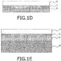
- FIGs. 1C and 1D are explanatory views showing an example of the step (B1) of the method for manufacturing an image display device.
- the photocurable resin composition layer 3 formed in step (A1) is irradiated with light (preferably ultraviolet light) to perform pre-curing, thereby forming the pre-cured resin layer 5.
- the purpose of the pre-curing of the photocurable resin composition layer 3 is to change the state of the photocurable resin composition from a liquid state to a substantially nonflowable state to improve the handling property by preventing the photocurable resin composition from flowing out even when the top and bottom are reversed as shown in FIG. 1D .
- the light transmitting cured resin layer 3 between the light shielding layer 1 and the image display member can be sufficiently cured with light without being removed from therebetween, and curing shrinkage can be reduced.
- the pre-curing of the photocurable resin composition layer 3 is preferably performed so that the curing rate (gel fraction) of the pre-cured resin layer 5 is 10 to 90%, more preferably 40 to 90%, and still more preferably 70 to 90%.
- the curing rate (gel fraction) is a numerical value defined as a ratio (consumption rate) of the amount of (meth)acryloyl group present in the photocurable resin composition layer after the ultraviolet irradiation to the amount of (meth)acryloyl group present before the ultraviolet irradiation, and the larger this numerical value is, the more curing progresses.
- the conditions of the ultraviolet irradiation such as the type of the light source, output power, illuminance, integrated light quantity, and the like are not particularly limited as long as the curing rate (gel fraction) of the pre-curing is preferably 10 to 90%, and a known photoradical polymerization process condition of (meth)acrylate by ultraviolet irradiation can be employed.
- ultraviolet irradiation is preferably performed using a UV-LED under a condition of an illuminance of 100 to 300 mW/cm 2 and an integrated light quantity of 100 to 300 mJ/cm 2 .
- a condition of the ultraviolet irradiation is preferably selected so that no dripping or deformation of the pre-cured resin layer 5 occurs during the laminating process in step (C1) to be described later within the range of the above curing rate.
- the viscosity is preferably 20 Pa*S or more (cone plate rheometer, 25 °C, cone and plate C 35/2, rotation speed 10 rpm).
- step (CI) the image display member and the light transmitting optical member are bonded to each other via the pre-cured resin layer.
- FIG. 1E is an explanatory view showing an example of the step (C1) of the method for manufacturing an image display device.
- the light transmitting optical member 2 is bonded to the image display member 6 on the side of the pre-cured resin layer 5.
- the bonding can be carried out, for example, by applying pressure at 10 to 80 °C using a known pressure bonding device.
- step (D1) the pre-cured resin layer disposed between the image display member and the light transmitting optical member is irradiated with light and is final-cured, whereby the image display member and the light transmitting optical member are laminated via the light transmitting cured resin layer to complete an image display device.
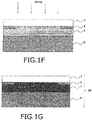
- FIGs. 1F and 1G are explanatory views showing an example of the step (D1) of the method for manufacturing an image display device.
- the pre-cured resin layer 5 sandwiched between the image display member 6 and the light transmitting optical member 2 is irradiated with light (preferably ultraviolet light) and is final-cured.
- the pre-cured resin layer 5 is final-cured to sufficiently cure the pre-cured resin layer 5 so that the image display member 6 and the light transmitting optical member 2 are bonded and laminated.
- the image display member 6 and the light transmitting optical member 2 are laminated with the light transmitting cured resin layer 7 interposed therebetween to form an image display device 10 as shown in FIG. 1G .
- the pre-cured resin layer 5 between the light shielding layer 1 of the light transmitting optical member 2 and the image display member 6 may be final-cured by irradiating the pre-cured resin layer 5 with light.
- the final-curing is preferably performed so that the curing rate (gel fraction) of the light transmitting cured resin layer 7 is 90% or more, more preferably 95% or more.
- the conditions of the final-curing such as the type of the light source, output power, illuminance, integrated light quantity, and the like are not particularly limited, and a known photo-radical polymerization process condition of (meth)acrylate by irradiation with ultraviolet light may be employed.
- ultraviolet irradiation is preferably performed using an ultraviolet irradiator (metal halide lamps, highpressure mercury, UV-LEDs, etc.) under a condition of an illuminance of 50 to 300 mW/cm 2 and an integrated light quantity of 1,000 to 3,000 mJ/cm 2 .
- an ultraviolet irradiator metal halide lamps, highpressure mercury, UV-LEDs, etc.
- the image display member 6 examples include a liquid crystal display panel, an organic EL display panel, a plasma display panel, and a touch panel.
- the touch panel means an image display/input panel that combines a display element such as a liquid crystal display panel and a position input device such as a touch pad.
- the light transmitting cured resin layer 7 preferably has a shear storage modulus of 2,000 to 320,000 Pa. It should be noted that the shear storage modulus of the light transmitting cured resin layer 7 is a value at 25 °C. By setting the shear storage modulus of the light transmitting cured resin layer 7 within the above-mentioned range, the shear storage modulus of the pre-cured resin layer 5 before the final-curing can be in an appropriate range, that is, the pre-cured resin layer 5 can be in a low elasticity state. As a result, as shown in FIG.
- the light transmitting optical member 2 when the light transmitting optical member 2 is bonded to the image display member 6 on the side of the pre-cured resin layer 5, the light transmitting optical member 2 can be bonded at a lower bonding pressure, thus reducing damage caused by pressing the image display member 6 and the light transmitting optical member 2.
- the light transmitting cured resin layer 7 may be in any configuration as long as it has a light transmitting property so that the image formed on the image display member 6 can be viewed therethrough.
- step (A2) a photocurable resin composition is applied to a surface of an image display member to form a photocurable resin composition layer.
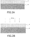
- FIG. 2A is an explanatory view showing an example of the step (A2) of the method for manufacturing an image display device.
- a photocurable resin composition is applied to a surface of the image display member 6 so that the resulting surface is flat to form a photocurable resin composition layer 3.
- the thickness of the photocurable resin composition layer 3 is preferably selected to cancel the height difference formed between the light shielding layer and the light shielding layer-forming side surface of the light transmitting optical member.
- the thickness of the photocurable resin composition layer 3 is preferably 2.5 to 40 times the thickness of the light shielding layer, more preferably 2.5 to 12.5 times, and still more preferably 2.5 to 4 times.
- the application of the photocurable resin composition may be performed once or a plurality of times as long as a necessary thickness is achieved.
- step (B2) the photocurable resin composition layer formed in step (A2) is irradiated with light to perform a pre-curing, thereby forming a pre-cured resin layer.
- FIGs. 2B and 2C are explanatory views showing an example of the step (B2) of the method for manufacturing an image display device.
- the photocurable resin composition layer 3 formed in step (A2) is irradiated with light (preferably ultraviolet light) to cause pre-curing, thereby forming the pre-cured resin layer 5 ( FIG. 2C ).
- the pre-curing of the photocurable resin composition layer 3 is preferably performed so that the curing rate (gel fraction) of the pre-cured resin layer 5 is 10 to 90%, more preferably 40 to 90%, and still more preferably 70 to 90%.
- step (C2) the image display member and the light transmitting optical member are bonded to each other via the pre-cured resin layer.
- FIG. 2D is an explanatory view showing an example of the step (C2) of the method for manufacturing an image display device.
- the light transmitting optical member 2 is bonded to the pre-cured resin layer 5 of the image display member 6 on the light shielding layer 1 side.
- the bonding can be carried out, for example, by applying pressure at 10 to 80 °C using a known pressure bonding device.
- step (D2) a pre-cured resin layer disposed between the image display member and the light transmitting optical member is irradiated with light and is final-cured, whereby the image display member and the light transmitting optical member are laminated via the light transmitting cured resin layer to complete an image display device.
- FIGs. 2E and 2F are explanatory views showing an example of the step (D2) of the method for manufacturing an image display device.
- the pre-cured resin layer 5 sandwiched between the image display member 6 and the light transmitting optical member 2 is irradiated with ultraviolet rays and is final-cured.
- the image display member 6 and the light transmitting optical member 2 are laminated with the light transmitting cured resin layer 7 interposed therebetween to form an image display device 10 as shown in FIG. 2F .
- the lifting phenomenon can be suppressed by containing a predetermined amount of a (meth)acrylate monomer having a ring structure as an acrylic monomer in the photocurable resin composition.
- the photocurable resin composition according to the present embodiment is a photocurable resin composition used in the method for manufacturing an image display device according to the first embodiment or the second embodiment.
- the photocurable resin composition contains a total of 31 to 55 mass% of a radical polymerizable component containing an acrylic oligomer and an acrylic monomer and 40 to 66 mass% of a plasticizer, 8 to 19 mass% of a (meth)acrylate monomer having a ring structure as the acrylic monomer, and the shear storage modulus after curing is 1,000 to 320,000 Pa. With this configuration, the lifting phenomenon can be suppressed.
- the light transmitting cured resin layer according to the present embodiment is a light transmitting cured resin layer used in the method for manufacturing an image display device according to the first embodiment or the second embodiment.
- the light transmitting cured resin layer contains a total of 31 to 55 mass% of a radical-polymerizable component containing an acrylic oligomer and an acrylic monomer, 40 to 66 mass% of a plasticizer, and 8 to 19 mass% of a (meth)acrylate monomer having a ring structure as the acrylic monomer, and having a shear storage modulus of 1,000 to 320,000 Pa. With this configuration, the lifting phenomenon can be suppressed.
- an image display device is manufactured by the method for manufacturing an image display device according to the first embodiment. Then, the lifting phenomenon of the pre-cured resin layer and the shear storage modulus of the light transmitting cured resin layer were evaluated. It should be noted that present technology is not limited to these examples.
- a light shielding layer having a width of 4 mm is applied on the entire periphery of the glass plate by a screen printing method using a thermosetting black ink (MRX ink available from Teikoku Ink Mfg.) and drying the light shielding layer so as to achieve an after-drying thickness of 40 ⁇ m to prepare a glass plate with a light shielding layer.
- MRX ink thermosetting black ink available from Teikoku Ink Mfg.
- the following components were uniformly mixed to prepare a photocurable resin composition.
- Hydrogenated polybutadiene having hydroxy groups at both terminal ends product name: GI-1000, GI-3000, KRASOL LBH-P-3000
- terpene resin 51 parts by mass in total
- the prepared photocurable resin composition was discharged onto the entire surface of the light shielding layer-forming side surface of the glass plate with the light shielding layer by using a resin dispenser to form a photocurable resin composition layer having an average thickness of 150 ⁇ m.
- the photocurable resin composition layer was pre-cured by irradiating the photocurable resin composition layer with ultraviolet light of 170 mW/cm 2 intensity using an ultraviolet irradiation device (UV-LED, product name H-16 LH4-V1-SM1, available from HOYA CANDEO OPTRONICS) so that the integrated light quantity was 280 mJ/cm 2 , thereby forming a pre-cured resin layer.
- UV-LED ultraviolet irradiation device
- the curing rate of the pre-cured resin layer was about 80 to 90% as determined using an absorption peak height of 1,640 to 1,620 cm -1 from the baseline in the FT-IR measurement chart as an index.
- the glass plate obtained in the step (B) was placed on a surface where a polarizing plate of a liquid crystal display element having a size of 40 (W) x 70 (L) mm was laminated so that the pre-cured resin layer side of the glass plate was on the polarizing plate side, and the glass plate was pressed by a rubber roller on the glass plate side to bond the glass plate.
- the liquid crystal display element obtained in step (C) was irradiated with ultraviolet rays (200 mW/cm 2 ) from the glass plate side by using an ultraviolet irradiation device (metal halide lamps available from USHIO) so that the integrated light quantity was 1,000 mJ/cm 2 or more, and the pre-cured resin layer was final-cured to form a light transmitting cured resin layer.
- the curing rate of the light transmitting cured resin layer was 97%.
- a liquid crystal display device was obtained in which a glass plate as a light transmitting optical member was laminated on a liquid crystal display element via a light transmitting cured resin layer.
- a liquid crystal display device was prepared in the same manner as in Example 1 except that the composition of the photocurable resin composition in Example 1 was changed as follows.
- Hydrogenated polybutadiene having hydroxy groups at both terminal ends product name: GI-1000, GI-3000, KRASOL LBH-P-3000
- terpene resin 54.6 parts by mass in total
- a liquid crystal display device was prepared in the same manner as in Example 1 except that the composition of the photocurable resin composition in Example 1 was changed as follows.
- Dicyclopentenyloxyethyl acrylate 8 parts by mass
- Isobornyl acrylate 6 parts by mass
- Benzyl acrylate 5 parts by mass
- Hydrogenated polybutadiene having hydroxy groups at both terminal ends product name: GI-1000, GI-3000, KRASOL LBH-P-3000
- terpene resin 40.6 parts by mass in total
- a liquid crystal display device was prepared in the same manner as in Example 1 except that the composition of the photocurable resin composition in Example 1 was changed as follows.
- Hydrogenated polybutadiene having hydroxy groups at both terminal ends product name: GI-1000, GI-3000, KRASOL LBH-P-3000
- terpene resin 52.85 parts by mass in total
- a liquid crystal display device was prepared in the same manner as in Example 4, except that an equal amount of dicyclopentanyl acrylate was used instead of dicyclopentenyl acrylate in the composition of the photocurable resin composition in Example 4.
- a liquid crystal display device was prepared in the same manner as in Example 4, except that an equal amount of isobornyl acrylate was used instead of dicyclopentenyl acrylate in the composition of the photocurable resin composition in Example 4.
- a liquid crystal display device was prepared in the same manner as in Example 4, except that an equal amount of tetrahydrofurfuryl acrylate was used instead of dicyclopentenyl acrylate in the composition of the photocurable resin composition in Example 4.
- a liquid crystal display device was prepared in the same manner as in Example 4, except that an equal amount of benzyl acrylate was used instead of dicyclopentenyl acrylate in the composition of the photocurable resin composition in Example 4.
- a liquid crystal display device was prepared in the same manner as in Example 1 except that the composition of the photocurable resin composition in Example 1 was changed as follows.
- Hydrogenated polybutadiene having hydroxy groups at both terminal ends product name: GI-1000, GI-3000, KRASOL LBH-P-3000
- terpene resin 66 parts by mass in total
- a liquid crystal display device was prepared in the same manner as in Example 1 except that the composition of the photocurable resin composition in Example 1 was changed as follows.
- a liquid crystal display device was prepared in the same manner as in Example 1 except that the composition of the photocurable resin composition in Example 1 was changed as follows.
- Hydrogenated polybutadiene having hydroxy groups at both terminal ends product name: GI-1000, GI-3000, KRASOL LBH-P-3000
- terpene resin 51.4 parts by mass in total
- a liquid crystal display device was prepared in the same manner as in Example 1 except that the composition of the photocurable resin composition in Example 1 was changed as follows.
- Hydrogenated polybutadiene having hydroxy groups at both terminal ends product name: GI-1000, GI-3000, KRASOL LBH-P-3000
- terpene resin 55.7 parts by mass in total
- a liquid crystal display device was prepared in the same manner as in Example 4, except that an equal amount of lauryl acrylate was used instead of dicyclopentenyl acrylate in the composition of the photocurable resin composition in Example 4.
- a liquid crystal display device was prepared in the same manner as in Example 4, except that an equal amount of n-octyl acrylate was used instead of dicyclopentenyl acrylate in the composition of the photocurable resin composition in Example 4.
- a liquid crystal display device was prepared in the same manner as in Example 4, except that an equal amount of octyl/decyl acrylate was used instead of dicyclopentenyl acrylate in the composition of the photocurable resin composition in Example 4.
- a liquid crystal display device was prepared in the same manner as in Example 4, except that an equal amount of isostearyl acrylate was used instead of dicyclopentenyl acrylate in the composition of the photocurable resin composition in Example 4.
- a liquid crystal display device was prepared in the same manner as in Example 4, except that an equal amount of isodecyl acrylate was used instead of dicyclopentenyl acrylate in the composition of the photocurable resin composition in Example 4.
- a liquid crystal display device was prepared in the same manner as in Example 1 except that the composition of the photocurable resin composition in Example 1 was changed as follows.
- Terpene resin 53 parts by mass
- a liquid crystal display device was prepared in the same manner as in Comparative Example 7, except that, in step (B) of Comparative Example 7, a photocurable resin composition layer was pre-cured by irradiating ultraviolet light of 344 mW/cm 2 intensity so that the integrated light quantity was 290 mJ/cm 2 , thereby forming a pre-cured resin layer.
- a liquid crystal display device was prepared in the same manner as in Comparative Example 7, except that, in step (B) of Comparative Example 7, a photocurable resin composition layer was pre-cured by irradiating ultraviolet light of 513 mW/cm 2 intensity so that the integrated light quantity was 297 mJ/cm 2 , thereby forming a pre-cured resin layer.
- a liquid crystal display device was prepared in the same manner as in Comparative Example 7, except that, in step (B) of Comparative Example 7, a photocurable resin composition layer was pre-cured by irradiating ultraviolet light of 852 mW/cm 2 intensity so that the integrated light quantity was 309 mJ/cm 2 , thereby forming a pre-cured resin layer.
- a liquid crystal display device was prepared in the same manner as in Comparative Example 7, except that, in step (B) of Comparative Example 7, a photocurable resin composition layer was pre-cured by irradiating ultraviolet light of 852 mW/cm 2 intensity so that the integrated light quantity was 3,696 mJ/cm 2 , thereby forming a pre-cured resin layer.
- a liquid crystal display device was prepared in the same manner as in Comparative Example 7, except that, in step (B) of Comparative Example 7, a photocurable resin composition layer was pre-cured by irradiating ultraviolet light of 170 mW/cm 2 intensity so that the integrated light quantity was 1,169 mJ/cm 2 , thereby forming a pre-cured resin layer.
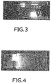
- FIG. 3 is a plan view showing an example of the appearance of the pre-cured resin layer when the evaluation of the lifting phenomenon is OK.
- FIG. 4 is a plan view showing an example of the appearance of the pre-cured resin layer when the evaluation of the lifting phenomenon is NG. The results are shown in the following table.
- the shear storage modulus of the light transmitting cured resin layer was calculated using a viscoelasticity measuring device.
- the measurement conditions were set to a measurement temperature range of 20 to 25 °C, a frequency of 1 Hz, and a strain of 0.1%. The results are shown in the following table.
- a photocurable resin composition contains a total of 31 to 55 mass% of a radical polymerizable component containing an acrylic oligomer and an acrylic monomer and 40 to 66 mass% of a plasticizer
- the acrylic monomer contains 5 to 19 mass% of a (meth)acrylate monomer having a cyclic hydrocarbon group
- the shear storage modulus of the light transmitting cured resin layer is 1,000 to 320,000
Landscapes
- Chemical & Material Sciences (AREA)
- Organic Chemistry (AREA)
- Physics & Mathematics (AREA)
- Health & Medical Sciences (AREA)
- Chemical Kinetics & Catalysis (AREA)
- Medicinal Chemistry (AREA)
- Polymers & Plastics (AREA)
- Nonlinear Science (AREA)
- Engineering & Computer Science (AREA)
- General Physics & Mathematics (AREA)
- Optics & Photonics (AREA)
- Theoretical Computer Science (AREA)
- Crystallography & Structural Chemistry (AREA)
- Mathematical Physics (AREA)
- Manufacturing & Machinery (AREA)
- Devices For Indicating Variable Information By Combining Individual Elements (AREA)
- Macromonomer-Based Addition Polymer (AREA)
- Electroluminescent Light Sources (AREA)
- Adhesives Or Adhesive Processes (AREA)
- Liquid Crystal (AREA)
Abstract
Description
- The present disclosure relates to a method for manufacturing an image display device by bonding and laminating an image display member such as a liquid crystal display panel and a light transmitting optical member such as a transparent protective sheet disposed on the surface of the display member via a light transmitting cured resin layer. This application claims priority on the basis of Japanese Patent Application No.
2017 -125891 - In an image display device such as a liquid crystal display panel used for an information terminal such as a smartphone, a photocurable resin composition layer is formed by arranging a photocurable resin composition between an image display member such as a liquid crystal display panel or an organic EL panel and a light transmitting optical member. Thereafter, the photocurable resin composition layer is cured by irradiating the photocurable resin composition layer with light to form a light transmitting cured resin layer. In this way, image display devices are manufactured by bonding and laminating the image display member and the light transmitting optical member.
- A light shielding layer is usually provided at a peripheral portion of the image display surface of the light transmitting optical member in order to improve the brightness and contrast of a display image. Therefore, the curing of the photocurable resin composition sandwiched between the light shielding layer and the image display member does not progress sufficiently, so that sufficient adhesive strength may not be obtained in some cases. As a result, there is a concern that separation between the light transmitting optical member and the image display member and invasion of moisture into the gap may deteriorate image quality.
- Thus, for example, a method for manufacturing a display device has been proposed which includes a first irradiation step (pre-curing step) of irradiating light to an adhesive applied to at least one of a display panel and a substrate, a bonding step of bonding the display panel and the substrate after the first irradiation step, and a second irradiation step (final-curing step) of irradiating light to the adhesive after the bonding step (PLT 1).
- PLT1: International Publication No.
WO 2009/054168 - When the image display member and the light transmitting optical member are bonded to each other after the pre-curing step of the photocurable resin composition, it is preferable that the surface layer portion of the pre-cured adhesive is as flat as possible from the viewpoints of more effective expression of the adhesive force with the members to be bonded and ensuring a sufficient adhesive area. In addition, in consideration of the reduction of damages caused by pressing against the image display member and the light transmitting optical member which are the adherends, it is preferable that the adherends can be adhered with a smaller bonding pressure. That is, the photocurable resin composition is preferably lower in elasticity.
- However, in order to reduce the elasticity of the photocurable resin composition, the crosslinking density of the photocurable resin composition is also reduced. Further, when curing of the outermost surface of the photocurable resin composition layer in the pre-cured state is insufficient, a so-called lifting phenomenon occurs. This lifting phenomenon is considered to be caused by the fact that an uncured component such as a polymerizable monomer existing in an insufficiently cured region permeates into the resin in the cured region and swells, resulting in wrinkles.
- This technology has been proposed in view of such a conventional situation, and provides a method for manufacturing an image display device capable of suppressing the lifting phenomenon. Also provided are a photocurable resin composition and a light transmitting cured resin layer.
- As a result of intensive studies, the present inventors found that the above problem can be solved by containing a predetermined amount of a (meth)acrylate monomer having a ring structure as an acrylic monomer in the photocurable resin composition.
- Specifically, a method for manufacturing an image display device according to the present technology includes the following steps (A) to (D), wherein the photocurable resin composition contains a total of 31 to 55 mass% of a radical polymerizable component containing an acrylic oligomer and an acrylic monomer and 40 to 66 mass% of a plasticizer, and contains 5 to 19 mass% of a (meth)acrylate monomer having a ring structure as the acrylic monomer, and the light transmitting cured resin layer has a shear storage modulus of 1,000 to 320,000 Pa.
- A step of applying a photocurable resin composition to a surface of a light transmitting optical member or a surface of an image display member to form a photocurable resin composition layer.
- A step of pre-curing by irradiating the photocurable resin composition layer with light to form a pre-cured resin layer.
- A step of bonding the image display member and the light transmitting optical member via the pre-cured resin layer.
- A step of obtaining an image display device by irradiating light to the pre-cured resin layer disposed between the image display member and the light transmitting optical member to final-cure the pre-cured resin layer, thereby laminating the image display member and the light transmitting optical member via the light transmitting cured resin layer.
- A photocurable resin composition according to the present technology includes: a total of 31 to 55 mass% of a radical polymerizable component containing an acrylic oligomer and an acrylic monomer and 40 to 66 mass% of a plasticizer; and 8 to 19 mass% of a (meth)acrylate monomer having a ring structure as the acrylic monomer, wherein a shear storage modulus of the photocurable resin composition after curing is 1,000 to 320,000 Pa.
- A light transmitting cured resin layer according to the present technology includes: a total of 31 to 55 mass% of a radical-polymerizable component containing an acrylic oligomer and an acrylic monomer, 40 to 66 mass% of a plasticizer, and 8 to 19 mass% of a (meth)acrylate monomer having a ring structure as the acrylic monomer, and having a shear storage modulus of 1,000 to 320,000 Pa.
- The present technology can suppress resin swelling by containing a predetermined amount of a (meth)acrylate monomer having a ring structure as an acrylic monomer in the photocurable resin composition, because, when the photocurable resin composition is pre-cured, an uncured component present in an insufficiently cured region of the photocurable resin composition is less likely to permeate into the cured resin due to the (meth)acrylate monomer having a ring structure as a bulky skeleton. That is, the present technology can suppress the lifting phenomenon.
-
-
FIG. 1A is an explanatory view showing an example of a step (A1) of a method for manufacturing an image display device according to the present embodiment. -
FIG. 1B is an explanatory view of a step (A1) of the method for manufacturing an image display device according to the present embodiment. -
FIG. 1C is an explanatory view of a step (B1) of the method for manufacturing an image display device according to the present embodiment. -
FIG. 1D is an explanatory view of a step (B1) of the method for manufacturing an image display device according to the present embodiment. -
FIG. 1E is an explanatory view of a step (C1) of the method for manufacturing an image display device according to the present embodiment. -
FIG. 1F is an explanatory view of a step (D1) of the method for manufacturing an image display device according to the present embodiment. -
FIG. 1G is an explanatory view of a step (D1) of the method for manufacturing an image display device according to the present embodiment. -
FIG. 2A is an explanatory view of a step (A2) of the method for manufacturing an image display device according to the present embodiment. -
FIG. 2B is an explanatory view of a step (B2) of the method for manufacturing an image display device according to the present embodiment. -
FIG. 2C is an explanatory view of a step (B2) of the method for manufacturing an image display device according to the present embodiment. -
FIG. 2D is an explanatory view of a step (C2) of the method for manufacturing an image display device according to the present embodiment. -
FIG. 2E is an explanatory view of a step (D2) of the method for manufacturing an image display device according to the present embodiment. -
FIG. 2F is an explanatory view of a step (D2) of the method for manufacturing an image display device according to the present embodiment. -
FIG. 3 is a plan view showing an example of an appearance of a pre-cured resin layer when the evaluation of the lifting phenomenon is OK. -
FIG. 4 is a plan view showing an example of an appearance of a pre-cured resin layer when the evaluation of the lifting phenomenon is NG. - Hereinafter, embodiments of the present invention will be described in detail. First, a method for manufacturing an image display device will be described in detail for each step in the order of the first embodiment and then the second embodiment with reference to the drawings.
- The method for manufacturing an image display device includes a step (A1) of applying a photocurable resin composition to a surface of an image display member to form a photocurable resin composition layer.
-
FIGs. 1A and 1B are explanatory views showing an example of step (A1) of the method for manufacturing an image display device. First, as shown inFIG. 1A , a light transmittingoptical member 2 having alight shielding layer 1 formed on a peripheral portion of one side is prepared. Next, as shown in FIG. IB, a photocurableresin composition layer 3 is formed by applying a photocurable resin composition to thesurface 2a of the light transmittingoptical member 2 to cancel a height difference 4 formed between thelight shielding layer 1 and the light shielding layer-formingside surface 2a of the light transmittingoptical member 2. Specifically, it is preferable to apply the photocurable resin composition to the entire surface of the light shielding layer-formingside surface 2a of the light transmittingoptical member 2, including the surface of thelight shielding layer 1, so that the resulting surface is flat without any height difference. The thickness of the photocurableresin composition layer 3 is preferably 1.2 to 50 times the thickness of thelight shielding layer 1, and more preferably 2 to 30 times the thickness. - It should be noted that the application of the photocurable resin composition may be performed once or a plurality of times as long as a necessary thickness is achieved.
- The
light shielding layer 1 is provided, for example, to improve the contrast of an image. Thelight shielding layer 1 is formed by applying a paint colored black or the like by a screen printing method or the like, and drying and curing the paint. The thickness of thelight shielding layer 1 is usually 5 to 100 µm. The thickness of thelight shielding layer 1 corresponds to the height difference 4. - The light transmitting
optical member 2 may be formed of any material as long as the material has a light transmitting property such that an image displayed on the image display member is visible. For example, a plate-like material or a sheet-like material such as glass, acrylic resin, polyethylene terephthalate, polyethylene naphthalate, and polycarbonate may be used, and a structure such as a touch panel in which sheet members are laminated may be used. These materials may be treated on one or both sides such as with a hard coating or anti-reflective treatment. Physical properties such as the thickness and elastic modulus of the light transmittingoptical member 2 may be appropriately selected according to the purpose of use. - The photocurable resin composition is preferably in a liquid state. By using a liquid material, the height difference 4 formed between the
light shielding layer 1 and the light shielding layer-formingside surface 2a of the light transmittingoptical member 2 can be more reliably canceled. The term "liquid state" preferably means a state having a viscosity of 0.01 to 100 Pa*s at 25 °C as measured by a Brookfield type (B-type) viscometer. - The photocurable resin composition preferably contains a radical polymerizable component containing an acrylic oligomer and an acrylic monomer, a photopolymerization initiator, and a plasticizer.
- The total content of the radical polymerizable component in the photocurable resin composition is 31 to 55 mass%, preferably 40 to 55 mass%.
- The acrylic oligomer is a base material of the photocurable resin composition, and a (meth)acrylate oligomer having polyisoprene, polyurethane, polybutadiene and the like as a skeleton thereof is preferable. As used herein, the term (meth)acrylate includes both acrylate and methacrylate.
- Specific examples of the (meth)acrylate oligomers having a polyisoprene skeleton include esterified products of polyisoprene polymer with maleic anhydride adduct and 2-hydroxyethyl methacrylate (product name: UC102 (molecular weight: 17,000 in terms of polystyrene) available from Kuraray; product name: UC203 (molecular weight: 35,000 in terms of polystyrene) available from Kuraray; and product name: UC-1 (molecular weight: 25,000) available from Kuraray), among others.
- Examples of the (meth)acrylic-type oligomers having a polyurethane backbone include aliphatic urethane acrylate (EBECRYL 230 (molecular weight of 5,000) available from Daicel Allnex; and UA-1 available from Light Chemical Industry), among others.
- As the (meth)acrylate oligomer having a polybutadiene skeleton, known oligomers may be employed.
- The content of the acrylic oligomer in the photocurable resin composition is preferably 5 to 30 mass%. When two or more acrylic oligomers are used in combination, it is preferable that the total amount of the acrylic oligomers satisfies the above range.
- The acrylic monomer is used as a reactive diluent for imparting sufficient reactivity and coating property, among other properties, to the photocurable resin composition in a manufacturing process of an image display device. The acrylic monomer contains at least a (meth)acrylate monomer having a ring structure, and may further contain other acrylic monomers. The content of the (meth)acrylate monomer having a ring structure in the photocurable resin composition is 5 to 19 mass%, may be 5 to 12 mass%, or may be 8 to 10 mass%. With this structure, the lifting phenomenon can be suppressed during the pre-curing of the photocurable resin composition layer.
- The (meth)acrylate monomer having a ring structure preferably has at least one of an alicyclic hydrocarbon group, an aromatic hydrocarbon group, and a heterocycle as the ring structure. The (meth)acrylate monomer having a ring structure may be a monofunctional (meth)acrylate monomer or a polyfunctional (meth)acrylate monomer.
- In the (meth)acrylate monomer having an alicyclic hydrocarbon group, the carbon number of the alicyclic hydrocarbon group is preferably 4 to 30, more preferably 4 to 20, and still more preferably 8 to 14. The alicyclic hydrocarbon group may have a monocyclic structure or a polycyclic structure, but preferably have a polycyclic structure. The alicyclic hydrocarbon group may be saturated or unsaturated. The alicyclic hydrocarbon group may have a substituent.
- The (meth)acrylate monomer having an alicyclic hydrocarbon group preferably has a bridged alicyclic hydrocarbon group from the viewpoint of suppressing the lifting phenomenon. Specific examples include isobornyl (meth)acrylate, dicyclopentanyl (meth)acrylate, dicyclopentenyl (meth)acrylate, dicyclopentenyloxy (meth)acrylate, dicyclopentenyloxyethyl acrylate, adamantyl (meth)acrylate, 2-alkyl-2-adamantyl (meth)acrylate, 3-hydroxy-1-adamantyl (meth)acrylate, and 1-perfluoroadamantyl (meth)acrylate. Among these, dicyclopentenyloxyethyl acrylate, dicyclopentenyl acrylate, dicyclopentanyl acrylate, and isobornyl acrylate are preferred from the viewpoint of suppressing the lifting phenomenon.
- In the (meth)acrylate monomer having an aromatic hydrocarbon group, the carbon number of the aromatic hydrocarbon group is preferably 6 to 30, and more preferably 6 to 18. The aromatic hydrocarbon group may have a monocyclic structure or a polycyclic structure. The aromatic hydrocarbon group may have a substituent.
- Specific examples of (meth)acrylate monomers having an aromatic hydrocarbon group include monofunctional monomers such as benzyl (meth)acrylate, phenyl (meth)acrylate, phenoxyethyl (meth)acrylate, phenoxypolyethylene glycol (meth)acrylate, nonylphenoxypolyethylene glycol (meth)acrylate, phenoxypolypropylene glycol (meth)acrylate, 2-(meth)acryloyloxyethyl-2-hydroxypropyl phthalate, 2-hydroxy-3-phenoxypropyl (meth)acrylate, and polyfunctional monomers such as polycarbonate diol di (meth)acrylate, bisphenol A ethylene oxide adduct di (meth)acrylate, and bisphenol A propylene oxide adduct di (meth)acrylate. Among these, from the viewpoint of suppressing the lifting phenomenon, a monocyclic monomer is preferable, and specifically benzyl (meth)acrylate is preferable.
- The (meth)acrylate monomer having a heterocyclic ring preferably has at least one of a nitrogen atom, an oxygen atom, and a sulfur atom as heterocyclic heteroatoms, and more preferably has an oxygen atom. The number of carbon atoms constituting the heterocycle is preferably 3 to 10, and more preferably 3 to 8. The heterocycle may be a monocyclic structure or a polycyclic structure. If the heterocyclic ring is a polycyclic structure, it may be condensed. The heterocycle may have a substituent.
- Specific examples of the (meth)acrylate monomer having a heterocyclic ring include tetrahydrofurfuryl (meth)acrylate, 4-tetrahydropyranyl acrylate, and 2-tetrahydropyranyl methyl acrylate, wherein tetrahydrofurfuryl (meth)acrylate is preferred, and tetrahydrofurfuryl (meth)acrylate is more preferred. Only one kind of (meth)acrylate monomer having a ring structure may be used, or two or more kinds of acrylate monomers may be used in combination.
- Examples of other acrylic monomers other than the (meth)acrylate monomer having a ring structure include linear or branched (meth)acrylate monomers. Specific examples include 2-hydroxypropyl methacrylate, 4-hydroxybutyl acrylate, lauryl acrylate, n-octyl acrylate, isodecyl acrylate, isostearyl acrylate, and octyl/decyl acrylate, among others.
- The content of the other acrylic monomer in the photocurable resin composition is preferably 5 to 35 mass%. When two or more acrylic monomers are used in combination, it is preferable that the total amount thereof satisfies the above range.
- As the photopolymerization initiator, a known photoradical polymerization initiator can be used. Examples include 1-hydroxy-cyclohexyl phenyl ketone (Irgacure 184, available from BASF), 2-hydroxy-1-{4-[4-(2-Hydroxy-2-methyl-propyronyl) benzyl] phenyl}-2-methyl-1-propane-1-one (Irgacure 127, available from BASF), benzophenone, and acetophenone, among others. Only one kind of photopolymerization initiator may be used, or two or more kinds may be used in combination.
- The content of the photopolymerization initiator is preferably 0.1 to 5 parts by mass, more preferably 0.2 to 3 parts by mass, relative to the total 100 parts by mass of the radical polymerizable components. By setting such a range, it is possible to prevent insufficient curing at the time of ultraviolet irradiation and to prevent an increase in outgassing due to cleavage. When two or more photopolymerization initiators are used in combination, it is preferable that the total amount of the photopolymerization initiators satisfies the above range.
- The plasticizer is used to impart buffering properties to the cured resin layer and to reduce the curing shrinkage ratio of the photocurable resin composition. Further, the plasticizer does not substantially react with the acrylic oligomer and the acrylic monomer when irradiated with ultraviolet rays. Examples of the plasticizer include a solid tackifier and a liquid oil component. Only one kind of plasticizer may be used, or two or more kinds of plasticizer may be used in combination.
- Examples of solid tackifiers include terpene type resins such as terpene resins, terpene phenolic resins, and hydrogenated terpene resins, and rosin type resins such as natural rosin, polymerized rosin, rosin esters, and hydrogenated rosin, as well as terpene hydrogenated resins. In addition, non-reactive oligomers obtained by pre-polymerizing the above-mentioned acrylic monomers with a low molecular weight may also be used, and examples thereof include copolymers of butyl acrylate, 2-hexyl acrylate and acrylic acid, and copolymers of cyclohexyl acrylate and methacrylic acid, among others.
- Examples of the liquid oil component include polybutadiene oil and polyisoprene oil.
- The content of the plasticizer in the photocurable resin composition is 40 to 66 mass%, and may be 40 to 60 mass%. When two or more plasticizers are used in combination, it is preferable that the total amount thereof satisfies the above range.
- The photocurable resin composition may further contain a chain transfer agent for adjusting the molecular weight. Examples of chain transfer agents include 2-mercaptoethanol, lauryl mercaptan, glycidyl mercaptan, mercaptoacetic acid, 2-ethylhexyl thioglycolate, 2,3-dimethylcapto-1-propanol, and α-methylstyrene dimer.
- The photocurable resin composition may further contain an adhesion improving agent such as a silane coupling agent and an additive such as an antioxidant as required.
- In step (B1), the photocurable resin composition layer formed in step (A1) is irradiated with light to perform a pre-curing, thereby forming a pre-cured resin layer.
-
FIGs. 1C and1D are explanatory views showing an example of the step (B1) of the method for manufacturing an image display device. As shown inFIG. 1C , the photocurableresin composition layer 3 formed in step (A1) is irradiated with light (preferably ultraviolet light) to perform pre-curing, thereby forming thepre-cured resin layer 5. The purpose of the pre-curing of the photocurableresin composition layer 3 is to change the state of the photocurable resin composition from a liquid state to a substantially nonflowable state to improve the handling property by preventing the photocurable resin composition from flowing out even when the top and bottom are reversed as shown inFIG. 1D . Further, by performing the pre-curing, the light transmitting curedresin layer 3 between thelight shielding layer 1 and the image display member can be sufficiently cured with light without being removed from therebetween, and curing shrinkage can be reduced. - The pre-curing of the photocurable
resin composition layer 3 is preferably performed so that the curing rate (gel fraction) of thepre-cured resin layer 5 is 10 to 90%, more preferably 40 to 90%, and still more preferably 70 to 90%. Here, the curing rate (gel fraction) is a numerical value defined as a ratio (consumption rate) of the amount of (meth)acryloyl group present in the photocurable resin composition layer after the ultraviolet irradiation to the amount of (meth)acryloyl group present before the ultraviolet irradiation, and the larger this numerical value is, the more curing progresses. - Specifically, the curing rate (gel fraction) can be calculated by substituting an absorption peak height (X) of 1,640 to 1,620 cm-1 from the baseline in the FT-IR measurement chart of the photocurable resin composition layer before ultraviolet irradiation and an absorption peak height (Y) of 1,640 to 1,620 cm-1 from the baseline in the FT-IR measurement chart of the photocurable resin composition layer after ultraviolet irradiation into the following equation:

- The conditions of the ultraviolet irradiation such as the type of the light source, output power, illuminance, integrated light quantity, and the like are not particularly limited as long as the curing rate (gel fraction) of the pre-curing is preferably 10 to 90%, and a known photoradical polymerization process condition of (meth)acrylate by ultraviolet irradiation can be employed. In particular, ultraviolet irradiation is preferably performed using a UV-LED under a condition of an illuminance of 100 to 300 mW/cm2 and an integrated light quantity of 100 to 300 mJ/cm2.
- Further, a condition of the ultraviolet irradiation is preferably selected so that no dripping or deformation of the
pre-cured resin layer 5 occurs during the laminating process in step (C1) to be described later within the range of the above curing rate. For example, the viscosity is preferably 20 Pa*S or more (cone plate rheometer, 25 °C, cone and plate C 35/2,rotation speed 10 rpm). - In step (CI), the image display member and the light transmitting optical member are bonded to each other via the pre-cured resin layer.
-
FIG. 1E is an explanatory view showing an example of the step (C1) of the method for manufacturing an image display device. As shown in FIG. IE, the light transmittingoptical member 2 is bonded to theimage display member 6 on the side of thepre-cured resin layer 5. The bonding can be carried out, for example, by applying pressure at 10 to 80 °C using a known pressure bonding device. - In step (D1), the pre-cured resin layer disposed between the image display member and the light transmitting optical member is irradiated with light and is final-cured, whereby the image display member and the light transmitting optical member are laminated via the light transmitting cured resin layer to complete an image display device.
-
FIGs. 1F and 1G are explanatory views showing an example of the step (D1) of the method for manufacturing an image display device. As shown inFIG. 1F , thepre-cured resin layer 5 sandwiched between theimage display member 6 and the light transmittingoptical member 2 is irradiated with light (preferably ultraviolet light) and is final-cured. Thepre-cured resin layer 5 is final-cured to sufficiently cure thepre-cured resin layer 5 so that theimage display member 6 and the light transmittingoptical member 2 are bonded and laminated. Thus, theimage display member 6 and the light transmittingoptical member 2 are laminated with the light transmitting cured resin layer 7 interposed therebetween to form animage display device 10 as shown inFIG. 1G . If necessary, thepre-cured resin layer 5 between thelight shielding layer 1 of the light transmittingoptical member 2 and theimage display member 6 may be final-cured by irradiating thepre-cured resin layer 5 with light. - The final-curing is preferably performed so that the curing rate (gel fraction) of the light transmitting cured resin layer 7 is 90% or more, more preferably 95% or more. The conditions of the final-curing such as the type of the light source, output power, illuminance, integrated light quantity, and the like are not particularly limited, and a known photo-radical polymerization process condition of (meth)acrylate by irradiation with ultraviolet light may be employed. In particular, ultraviolet irradiation is preferably performed using an ultraviolet irradiator (metal halide lamps, highpressure mercury, UV-LEDs, etc.) under a condition of an illuminance of 50 to 300 mW/cm2 and an integrated light quantity of 1,000 to 3,000 mJ/cm2.
- Examples of the
image display member 6 include a liquid crystal display panel, an organic EL display panel, a plasma display panel, and a touch panel. Here, the touch panel means an image display/input panel that combines a display element such as a liquid crystal display panel and a position input device such as a touch pad. - The light transmitting cured resin layer 7 preferably has a shear storage modulus of 2,000 to 320,000 Pa. It should be noted that the shear storage modulus of the light transmitting cured resin layer 7 is a value at 25 °C. By setting the shear storage modulus of the light transmitting cured resin layer 7 within the above-mentioned range, the shear storage modulus of the
pre-cured resin layer 5 before the final-curing can be in an appropriate range, that is, thepre-cured resin layer 5 can be in a low elasticity state. As a result, as shown inFIG. 1 (E) , when the light transmittingoptical member 2 is bonded to theimage display member 6 on the side of thepre-cured resin layer 5, the light transmittingoptical member 2 can be bonded at a lower bonding pressure, thus reducing damage caused by pressing theimage display member 6 and the light transmittingoptical member 2. - The light transmitting cured resin layer 7 may be in any configuration as long as it has a light transmitting property so that the image formed on the
image display member 6 can be viewed therethrough. - As described above, in the first embodiment, an example was explained in which a photocurable resin composition is applied to the light shielding layer-forming side surface of the light transmitting optical member. In the following second embodiment, an example will be described in which a photocurable resin composition is applied to the surface of an image display member. It should be noted that, in the drawings, the same reference sign indicates the same component.
- Hereinafter, a second embodiment of the method for manufacturing an image display device will be described in detail for each process step with reference to the drawings.
- In step (A2), a photocurable resin composition is applied to a surface of an image display member to form a photocurable resin composition layer.
-
FIG. 2A is an explanatory view showing an example of the step (A2) of the method for manufacturing an image display device. As shown inFIG. 2A , a photocurable resin composition is applied to a surface of theimage display member 6 so that the resulting surface is flat to form a photocurableresin composition layer 3. The thickness of the photocurableresin composition layer 3 is preferably selected to cancel the height difference formed between the light shielding layer and the light shielding layer-forming side surface of the light transmitting optical member. For example, the thickness of the photocurableresin composition layer 3 is preferably 2.5 to 40 times the thickness of the light shielding layer, more preferably 2.5 to 12.5 times, and still more preferably 2.5 to 4 times. - It should be noted that the application of the photocurable resin composition may be performed once or a plurality of times as long as a necessary thickness is achieved.
- In step (B2), the photocurable resin composition layer formed in step (A2) is irradiated with light to perform a pre-curing, thereby forming a pre-cured resin layer.
-
FIGs. 2B and2C are explanatory views showing an example of the step (B2) of the method for manufacturing an image display device. As shown inFIG. 2B , the photocurableresin composition layer 3 formed in step (A2) is irradiated with light (preferably ultraviolet light) to cause pre-curing, thereby forming the pre-cured resin layer 5 (FIG. 2C ). The pre-curing of the photocurableresin composition layer 3 is preferably performed so that the curing rate (gel fraction) of thepre-cured resin layer 5 is 10 to 90%, more preferably 40 to 90%, and still more preferably 70 to 90%. - In step (C2), the image display member and the light transmitting optical member are bonded to each other via the pre-cured resin layer.
-
FIG. 2D is an explanatory view showing an example of the step (C2) of the method for manufacturing an image display device. As shown inFIG. 2D , the light transmittingoptical member 2 is bonded to thepre-cured resin layer 5 of theimage display member 6 on thelight shielding layer 1 side. The bonding can be carried out, for example, by applying pressure at 10 to 80 °C using a known pressure bonding device. - In step (D2), a pre-cured resin layer disposed between the image display member and the light transmitting optical member is irradiated with light and is final-cured, whereby the image display member and the light transmitting optical member are laminated via the light transmitting cured resin layer to complete an image display device.
-
FIGs. 2E and 2F are explanatory views showing an example of the step (D2) of the method for manufacturing an image display device. As shown inFIG. 2E , thepre-cured resin layer 5 sandwiched between theimage display member 6 and the light transmittingoptical member 2 is irradiated with ultraviolet rays and is final-cured. Thus, theimage display member 6 and the light transmittingoptical member 2 are laminated with the light transmitting cured resin layer 7 interposed therebetween to form animage display device 10 as shown inFIG. 2F . - As described above, according to the present technology, the lifting phenomenon can be suppressed by containing a predetermined amount of a (meth)acrylate monomer having a ring structure as an acrylic monomer in the photocurable resin composition.
- The photocurable resin composition according to the present embodiment is a photocurable resin composition used in the method for manufacturing an image display device according to the first embodiment or the second embodiment. The photocurable resin composition contains a total of 31 to 55 mass% of a radical polymerizable component containing an acrylic oligomer and an acrylic monomer and 40 to 66 mass% of a plasticizer, 8 to 19 mass% of a (meth)acrylate monomer having a ring structure as the acrylic monomer, and the shear storage modulus after curing is 1,000 to 320,000 Pa. With this configuration, the lifting phenomenon can be suppressed.
- The light transmitting cured resin layer according to the present embodiment is a light transmitting cured resin layer used in the method for manufacturing an image display device according to the first embodiment or the second embodiment. The light transmitting cured resin layer contains a total of 31 to 55 mass% of a radical-polymerizable component containing an acrylic oligomer and an acrylic monomer, 40 to 66 mass% of a plasticizer, and 8 to 19 mass% of a (meth)acrylate monomer having a ring structure as the acrylic monomer, and having a shear storage modulus of 1,000 to 320,000 Pa. With this configuration, the lifting phenomenon can be suppressed.
- Examples of the present technology will be described below. In this technology, an image display device is manufactured by the method for manufacturing an image display device according to the first embodiment. Then, the lifting phenomenon of the pre-cured resin layer and the shear storage modulus of the light transmitting cured resin layer were evaluated. It should be noted that present technology is not limited to these examples.
- In this example, the following compounds were used.
- Aliphatic urethane acrylate, product name: EBECRYL 230, available from Daicel Allnex
- Dicyclopentenyloxyethyl acrylate, product name: FA-512 AS, available from Hitachi Chemical Company
Dicyclopentanyl acrylate, product name: FA-513 AS, available from Hitachi Chemical Company
Dicyclopentenyl acrylate, product name: FA-511 AS, available from Hitachi Chemical Company
Isobomyl acrylate, product name: IBXA, available from Osaka Organic Chemical Industry
Tetrahydrofurfuryl acrylate, product name: Biscoat#150, available from Osaka Organic Chemical
Benzyl acrylate, product name: Biscoat#160, available from Osaka Organic Chemical - 4-hydroxybutyl acrylate; product name: 4-HBA; available from BASF
Lauryl acrylate, product name: LA, available from Osaka Organic Chemical Industry
n-octyl acrylate; product name: NOAA, available from Osaka Organic Chemical Industry
Isodecyl acrylate; product name: FA-111A, available from Hitachi Chemical Company
Hydroxypropyl methacrylate; product name: Acriester HP (HPMA), available from Mitsubishi Rayon
Isostearyl acrylate, product name: ISTA, available from Osaka Organic Chemical
Octyl/decyl acrylate, product name: ODA-N, available from Daicel Allnex Plasticizer
Hydrogenated polybutadiene having hydroxy groups at both terminal ends, product name: GI-1000, GI-3000, available from Nippon Soda
Hydrogenated polybutadiene having hydroxy groups at both terminal ends, product name: KRASOL LBH-P-3000, available from CRAY VALLEY
Terpene resin, product name: Clearon M105, available from Yasuhara Chemical - 2,4,6-trimethylbenzoyl-diphenyl-phosphine oxide, product name LUCIRIN TPO, available from BASF
1-hydroxy-cyclohexyl-phenyl-ketone, product name: Irgacure 184, available from BASF - 3-methacryloxypropyltrimethoxysilane, product name: KBM-503, available from Shin-Etsu Silicone
3-mercaptopropyltrimethoxysilane, product name: KBM-803, available from Shin-Etsu Silicone
Hindered phenolic antioxidant, product name: IRGANOX 1010, available from BASF - After preparing a glass plate having a size of 45 (w) x 80 (1) x 0.4 (t) mm, a light shielding layer having a width of 4 mm is applied on the entire periphery of the glass plate by a screen printing method using a thermosetting black ink (MRX ink available from Teikoku Ink Mfg.) and drying the light shielding layer so as to achieve an after-drying thickness of 40 µm to prepare a glass plate with a light shielding layer.
- The following components were uniformly mixed to prepare a photocurable resin composition.
- Aliphatic urethane acrylate: 10 parts by mass
- Dicyclopentenyloxyethyl acrylate: 8.5 parts by mass
- 4-hydroxybutyl acrylate, lauryl acrylate, n-octyl acrylate, and isodecyl acrylate: 27 parts by mass in total
- Hydrogenated polybutadiene having hydroxy groups at both terminal ends (product name: GI-1000, GI-3000, KRASOL LBH-P-3000) and terpene resin: 51 parts by mass in total
- 2,4,6-trimethylbenzoyl-diphenyl-phosphine oxide and 1-hydroxy-cyclohexyl-phenyl-ketone: 3 parts by mass in total
- 3-methacryloxypropyltrimethoxysilane, 3-mercaptopropyltrimethoxysilane, and hindered phenolic antioxidant: 0.5 parts by mass in total
- The prepared photocurable resin composition was discharged onto the entire surface of the light shielding layer-forming side surface of the glass plate with the light shielding layer by using a resin dispenser to form a photocurable resin composition layer having an average thickness of 150 µm.
- The photocurable resin composition layer was pre-cured by irradiating the photocurable resin composition layer with ultraviolet light of 170 mW/cm2 intensity using an ultraviolet irradiation device (UV-LED, product name H-16 LH4-V1-SM1, available from HOYA CANDEO OPTRONICS) so that the integrated light quantity was 280 mJ/cm2, thereby forming a pre-cured resin layer.
- The curing rate of the pre-cured resin layer was about 80 to 90% as determined using an absorption peak height of 1,640 to 1,620 cm-1 from the baseline in the FT-IR measurement chart as an index.
- The glass plate obtained in the step (B) was placed on a surface where a polarizing plate of a liquid crystal display element having a size of 40 (W) x 70 (L) mm was laminated so that the pre-cured resin layer side of the glass plate was on the polarizing plate side, and the glass plate was pressed by a rubber roller on the glass plate side to bond the glass plate.
- The liquid crystal display element obtained in step (C) was irradiated with ultraviolet rays (200 mW/cm2) from the glass plate side by using an ultraviolet irradiation device (metal halide lamps available from USHIO) so that the integrated light quantity was 1,000 mJ/cm2 or more, and the pre-cured resin layer was final-cured to form a light transmitting cured resin layer. The curing rate of the light transmitting cured resin layer was 97%. Thus, a liquid crystal display device was obtained in which a glass plate as a light transmitting optical member was laminated on a liquid crystal display element via a light transmitting cured resin layer.
- A liquid crystal display device was prepared in the same manner as in Example 1 except that the composition of the photocurable resin composition in Example 1 was changed as follows.
- Aliphatic urethane acrylate: 6 parts by mass
- Dicyclopentenyloxyethyl acrylate: 8 parts by mass
- 4-hydroxybutyl acrylate, lauryl acrylate, n-octyl acrylate, and isodecyl acrylate: 28 parts by mass in total
- Hydrogenated polybutadiene having hydroxy groups at both terminal ends (product name: GI-1000, GI-3000, KRASOL LBH-P-3000) and terpene resin: 54.6 parts by mass in total
- 2,4,6-trimethylbenzoyl-diphenyl-phosphine oxide and 1-hydroxy-cyclohexyl-phenyl-ketone: 3 parts by mass in total
- 3-methacryloxypropyltrimethoxysilane, 3-mercaptopropyltrimethoxysilane, and hindered phenolic antioxidant: 0.4 parts by mass in total
- A liquid crystal display device was prepared in the same manner as in Example 1 except that the composition of the photocurable resin composition in Example 1 was changed as follows.
- Aliphatic urethane acrylate: 19 parts by mass
- Dicyclopentenyloxyethyl acrylate: 8 parts by mass
Isobornyl acrylate: 6 parts by mass
Benzyl acrylate: 5 parts by mass - 4-hydroxybutyl acrylate, lauryl acrylate, and hydroxypropyl methacrylate: 17 parts by mass in total
- Hydrogenated polybutadiene having hydroxy groups at both terminal ends (product name: GI-1000, GI-3000, KRASOL LBH-P-3000) and terpene resin: 40.6 parts by mass in total
- 2,4,6-trimethylbenzoyl-diphenyl-phosphine oxide and 1-hydroxy-cyclohexyl-phenyl-ketone: 3.8 parts by mass in total
- 3-methacryloxypropyltrimethoxysilane, 3-mercaptopropyltrimethoxysilane, and hindered phenolic antioxidant: 0.6 parts by mass in total
- A liquid crystal display device was prepared in the same manner as in Example 1 except that the composition of the photocurable resin composition in Example 1 was changed as follows.
- Aliphatic urethane acrylate: 11 parts by mass
- Dicyclopentenyl acrylate: 8.8 parts by mass
- 4-hydroxybutyl acrylate, lauryl acrylate, n-octyl acrylate, and isodecyl acrylate: 25 parts by mass in total
- Hydrogenated polybutadiene having hydroxy groups at both terminal ends (product name: GI-1000, GI-3000, KRASOL LBH-P-3000) and terpene resin: 52.85 parts by mass in total
- 2,4,6-trimethylbenzoyl-diphenyl-phosphine oxide and 1-hydroxy-cyclohexyl-phenyl-ketone: 2 parts by mass in total
- 3-methacryloxypropyltrimethoxysilane, 3 -mercaptopropyltrimethoxysilane, and hindered phenolic antioxidant: 0.35 parts by mass in total
- A liquid crystal display device was prepared in the same manner as in Example 4, except that an equal amount of dicyclopentanyl acrylate was used instead of dicyclopentenyl acrylate in the composition of the photocurable resin composition in Example 4.
- A liquid crystal display device was prepared in the same manner as in Example 4, except that an equal amount of isobornyl acrylate was used instead of dicyclopentenyl acrylate in the composition of the photocurable resin composition in Example 4.
- A liquid crystal display device was prepared in the same manner as in Example 4, except that an equal amount of tetrahydrofurfuryl acrylate was used instead of dicyclopentenyl acrylate in the composition of the photocurable resin composition in Example 4.
- A liquid crystal display device was prepared in the same manner as in Example 4, except that an equal amount of benzyl acrylate was used instead of dicyclopentenyl acrylate in the composition of the photocurable resin composition in Example 4.
- A liquid crystal display device was prepared in the same manner as in Example 1 except that the composition of the photocurable resin composition in Example 1 was changed as follows.
- Aliphatic urethane acrylate: 10.85 parts by mass
- Dicyclopentenyl acrylate: 8.8 parts by mass
- 4-hydroxybutyl acrylate and lauryl acrylate: 12 parts by mass in total Plasticizer
- Hydrogenated polybutadiene having hydroxy groups at both terminal ends (product name: GI-1000, GI-3000, KRASOL LBH-P-3000) and terpene resin: 66 parts by mass in total
- 2,4,6-trimethylbenzoyl-diphenyl-phosphine oxide and 1-hydroxy-cyclohexyl-phenyl-ketone: 2 parts by mass in total
- 3 -methacryloxypropyltrimethoxysilane, 3-mercaptopropyltrimethoxysilane, and hindered phenolic antioxidant: 0.35 parts by mass in total
- A liquid crystal display device was prepared in the same manner as in Example 1 except that the composition of the photocurable resin composition in Example 1 was changed as follows.
- Aliphatic urethane acrylate: 14 parts by mass
- Dicyclopentenyloxyethyl acrylate: 9 parts by mass
- 4-hydroxybutyl acrylate and lauryl acrylate: 34.65 parts by mass in total Plasticizer
Hydrogenated polybutadiene having hydroxy groups at both terminal ends (product name: GI-1000, GI-3000, KRASOL LBH-P-3000) and terpene resin: 40 parts by mass in total - 2,4,6-trimethylbenzoyl-diphenyl-phosphine oxide and 1-hydroxy-cyclohexyl-phenyl-ketone: 2 parts by mass in total
- 3-methacryloxypropyltrimethoxysilane and hindered phenolic antioxidant: 0.35 parts by mass in total
- A liquid crystal display device was prepared in the same manner as in Example 1 except that the composition of the photocurable resin composition in Example 1 was changed as follows.
- Aliphatic urethane acrylate: 10.3 parts by mass
- 4-hydroxybutyl acrylate, lauryl acrylate, n-octyl acrylate, isodecyl acrylate, and isostearyl acrylate: 36 parts by mass in total
- Hydrogenated polybutadiene having hydroxy groups at both terminal ends (product name: GI-1000, GI-3000, KRASOL LBH-P-3000) and terpene resin: 51.4 parts by mass in total
- 2,4,6-trimethylbenzoyl-diphenyl-phosphine oxide and 1-hydroxy-cyclohexyl-phenyl-ketone: 2 parts by mass in total
- 3-methacryloxypropyltrimethoxysilane, 3-mercaptopropyltrimethoxysilane, and hindered phenolic antioxidant: 0.3 parts by mass in total
- A liquid crystal display device was prepared in the same manner as in Example 1 except that the composition of the photocurable resin composition in Example 1 was changed as follows.
- Aliphatic urethane acrylate: 10.1 parts by mass
- Dicyclopentenyloxyethyl acrylate: 0.8 parts by mass
- 4-hydroxybutyl acrylate, lauryl acrylate, n-octyl acrylate, and isodecyl acrylate: 30 parts by mass in total
- Hydrogenated polybutadiene having hydroxy groups at both terminal ends (product name: GI-1000, GI-3000, KRASOL LBH-P-3000) and terpene resin: 55.7 parts by mass in total
- 2,4,6-trimethylbenzoyl-diphenyl-phosphine oxide and 1-hydroxy-cyclohexyl-phenyl-ketone: 3 parts by mass in total
- 3-methacryloxypropyltrimethoxysilane, 3-mercaptopropyltrimethoxysilane, and hindered phenolic antioxidant: 0.4 parts by mass in total
- A liquid crystal display device was prepared in the same manner as in Example 4, except that an equal amount of lauryl acrylate was used instead of dicyclopentenyl acrylate in the composition of the photocurable resin composition in Example 4.
- A liquid crystal display device was prepared in the same manner as in Example 4, except that an equal amount of n-octyl acrylate was used instead of dicyclopentenyl acrylate in the composition of the photocurable resin composition in Example 4.
- A liquid crystal display device was prepared in the same manner as in Example 4, except that an equal amount of octyl/decyl acrylate was used instead of dicyclopentenyl acrylate in the composition of the photocurable resin composition in Example 4.
- A liquid crystal display device was prepared in the same manner as in Example 4, except that an equal amount of isostearyl acrylate was used instead of dicyclopentenyl acrylate in the composition of the photocurable resin composition in Example 4.
- A liquid crystal display device was prepared in the same manner as in Example 4, except that an equal amount of isodecyl acrylate was used instead of dicyclopentenyl acrylate in the composition of the photocurable resin composition in Example 4.
- A liquid crystal display device was prepared in the same manner as in Example 1 except that the composition of the photocurable resin composition in Example 1 was changed as follows.
- Aliphatic urethane acrylate: 10.6 parts by mass
- 4-hydroxybutyl acrylate, lauryl acrylate, n-octyl acrylate, and isodecyl acrylate: 34 parts by mass in total
- Terpene resin: 53 parts by mass
- 2,4,6-trimethylbenzoyl-diphenyl-phosphine oxide and 1-hydroxy-cyclohexyl-phenyl-ketone: 2.1 parts by mass in total
- 3-methacryloxypropyltrimethoxysilane and hindered phenolic antioxidant: 0.3 parts by mass in total
- A liquid crystal display device was prepared in the same manner as in Comparative Example 7, except that, in step (B) of Comparative Example 7, a photocurable resin composition layer was pre-cured by irradiating ultraviolet light of 344 mW/cm2 intensity so that the integrated light quantity was 290 mJ/cm2, thereby forming a pre-cured resin layer.
- A liquid crystal display device was prepared in the same manner as in Comparative Example 7, except that, in step (B) of Comparative Example 7, a photocurable resin composition layer was pre-cured by irradiating ultraviolet light of 513 mW/cm2 intensity so that the integrated light quantity was 297 mJ/cm2, thereby forming a pre-cured resin layer.
- A liquid crystal display device was prepared in the same manner as in Comparative Example 7, except that, in step (B) of Comparative Example 7, a photocurable resin composition layer was pre-cured by irradiating ultraviolet light of 852 mW/cm2 intensity so that the integrated light quantity was 309 mJ/cm2, thereby forming a pre-cured resin layer.
- A liquid crystal display device was prepared in the same manner as in Comparative Example 7, except that, in step (B) of Comparative Example 7, a photocurable resin composition layer was pre-cured by irradiating ultraviolet light of 852 mW/cm2 intensity so that the integrated light quantity was 3,696 mJ/cm2, thereby forming a pre-cured resin layer.
- A liquid crystal display device was prepared in the same manner as in Comparative Example 7, except that, in step (B) of Comparative Example 7, a photocurable resin composition layer was pre-cured by irradiating ultraviolet light of 170 mW/cm2 intensity so that the integrated light quantity was 1,169 mJ/cm2, thereby forming a pre-cured resin layer.
- In the step (B) of each Example and Comparative Example, the appearance of the pre-cured resin layer was observed and the presence or absence of the lifting phenomenon was evaluated. When the lifting phenomenon did not occur, it was evaluated as OK, and when the lifting phenomenon occurred, it was evaluated as NG.
FIG. 3 is a plan view showing an example of the appearance of the pre-cured resin layer when the evaluation of the lifting phenomenon is OK.FIG. 4 is a plan view showing an example of the appearance of the pre-cured resin layer when the evaluation of the lifting phenomenon is NG. The results are shown in the following table. - The shear storage modulus of the light transmitting cured resin layer was calculated using a viscoelasticity measuring device. The measurement conditions were set to a measurement temperature range of 20 to 25 °C, a frequency of 1 Hz, and a strain of 0.1%. The results are shown in the following table.


- It has been found that, as in Examples 1 to 10, when a photocurable resin composition contains a total of 31 to 55 mass% of a radical polymerizable component containing an acrylic oligomer and an acrylic monomer and 40 to 66 mass% of a plasticizer, the acrylic monomer contains 5 to 19 mass% of a (meth)acrylate monomer having a cyclic hydrocarbon group, and the shear storage modulus of the light transmitting cured resin layer is 1,000 to 320,000, the lifting phenomenon can be suppressed.
- In contrast, it was found that lifting phenomenon occurs when the photocurable resin composition does not contain a (meth)acrylate monomer having a ring structure as in Comparative Examples 1 and 3 to 7.
- In addition, it was found that lifting phenomenon occurs when the content of the (meth)acrylate monomer having a ring structure in the photocurable resin composition is less than 5 mass% as in Comparative Example 2.
- Moreover, it was found that lifting phenomenon occurs even if the photocurable resin composition is prepared so that the shear storage modulus of the light transmitting cured resin layer after the final-curing is increased, when the photocurable resin composition does not contain a (meth)acrylate monomer having a ring structure as in Comparative Example 8.
- It was found that the lifting phenomenon occurs even if the illuminance and the integrated light quantity of the ultraviolet rays used for the pre-curing of the photocurable resin composition are changed when the photocurable resin composition does not contain a (meth)acrylate monomer having a ring structure as in Comparative Example 9 to 12.
- 1 Light shielding layer, 2 light transmitting optical member, 2a light shielding layer-forming side surface, 3 photocurable resin composition layer, 4 height difference, 5 pre-cured resin layer, 6 image display member, 7 light transmitting cured resin layer, 10 image display device
Claims (10)
- A method for manufacturing an image display device, comprising:a step (A) of applying a photocurable resin composition to a surface of a light transmitting optical member or a surface of an image display member to form a photocurable resin composition layer;a step (B) of pre-curing by irradiating the photocurable resin composition layer with light to form a pre-cured resin layer;a step (C) of bonding the image display member and the light transmitting optical member via the pre-cured resin layer; anda step (D) of obtaining an image display device by irradiating light to the pre-cured resin layer disposed between the image display member and the light transmitting optical member to final-cure the pre-cured resin layer, thereby laminating the image display member and the light transmitting optical member via the light transmitting cured resin layer,wherein the photocurable resin composition contains a total of 31 to 55 mass% of a radical polymerizable component containing an acrylic oligomer and an acrylic monomer and 40 to 66 mass% of a plasticizer, and contains 5 to 19 mass% of a (meth)acrylate monomer having a ring structure as the acrylic monomer, andwherein the light transmitting cured resin layer has a shear storage modulus of 1,000 to 320,000 Pa.
- The method for manufacturing an image display device according to claim 1, wherein the (meth)acrylate monomer having the ring structure has at least one of an alicyclic hydrocarbon group, an aromatic hydrocarbon group, and a heterocycle as the ring structure.
- The method for manufacturing an image display device according to claim 1 or 2, wherein the light transmitting cured resin layer has a shear storage modulus of 2,000 to 320,000 Pa.
- The method for manufacturing an image display device according to any one of claims 1 to 3, wherein the photocurable resin composition contains 8 to 10 mass% of a (meth)acrylate monomer having the ring structure.
- The method for manufacturing an image display device according to any one of claims 1 to 4, wherein in the step (B), the photocurable resin composition layer is irradiated with ultraviolet rays to pre-cure the photocurable resin composition layer so that the curing rate of the pre-cured resin layer is 70 to 90%
- The method for manufacturing an image display device according to any one of claims 1 to 5, wherein in the step (B), light irradiation is performed using a UV-LED under conditions of an illuminance of 100 to 300.mW/cm2 and an integrated light quantity of 100 to 300 mJ/cm2.
- The method for manufacturing an image display device according to any one of claims 1 to 6, wherein in the step (D), the pre-cured resin layer is final-cured by irradiating the pre-cured resin layer with ultraviolet rays so that the curing rate of the light transmitting cured resin layer is 90% or more.
- The method for manufacturing an image display device according to any one of claims 1 to 7, wherein the image display member is a liquid crystal display panel, an organic EL display panel, a plasma display panel, or a touch panel.
- A photocurable resin composition, comprising:a total of 31 to 55 mass% of a radical polymerizable component containing an acrylic oligomer and an acrylic monomer and 40 to 66 mass% of a plasticizer; and8 to 19 mass% of a (meth)acrylate monomer having a ring structure as the acrylic monomer,wherein a shear storage modulus of the photocurable resin composition after curing is 1,000 to 320,000 Pa.
- A light transmitting cured resin layer containing a total of 31 to 55 mass% of a radical-polymerizable component containing an acrylic oligomer and an acrylic monomer, 40 to 66 mass% of a plasticizer, and 8 to 19 mass% of a (meth)acrylate monomer having a ring structure as the acrylic monomer, and having a shear storage modulus of 1,000 to 320,000 Pa.
Applications Claiming Priority (2)
| Application Number | Priority Date | Filing Date | Title |
|---|---|---|---|
| JP2017125891A JP6370967B1 (en) | 2017-06-28 | 2017-06-28 | Method for manufacturing image display device, photocurable resin composition, and light transmissive cured resin layer |
| PCT/JP2018/023440 WO2019004020A1 (en) | 2017-06-28 | 2018-06-20 | Method for producing image display device, photocurable resin composition and light-transmitting cured resin layer |
Publications (3)
| Publication Number | Publication Date |
|---|---|
| EP3648084A1 true EP3648084A1 (en) | 2020-05-06 |
| EP3648084A4 EP3648084A4 (en) | 2021-03-17 |
| EP3648084B1 EP3648084B1 (en) | 2023-12-20 |
Family
ID=63104383
Family Applications (1)
| Application Number | Title | Priority Date | Filing Date |
|---|---|---|---|
| EP18824791.0A Active EP3648084B1 (en) | 2017-06-28 | 2018-06-20 | Method for producing image display device, photocurable resin composition and light-transmitting cured resin layer |
Country Status (7)
| Country | Link |
|---|---|
| US (1) | US12576628B2 (en) |
| EP (1) | EP3648084B1 (en) |
| JP (1) | JP6370967B1 (en) |
| KR (2) | KR20200011966A (en) |
| CN (1) | CN110945581B (en) |
| TW (1) | TWI791544B (en) |
| WO (1) | WO2019004020A1 (en) |
Families Citing this family (6)
| Publication number | Priority date | Publication date | Assignee | Title |
|---|---|---|---|---|
| JP7080144B2 (en) * | 2018-09-19 | 2022-06-03 | アイカ工業株式会社 | Photocurable adhesive resin composition |
| CN209590464U (en) * | 2019-02-02 | 2019-11-05 | 合肥京东方显示技术有限公司 | A kind of color membrane substrates and display device |
| KR102473023B1 (en) * | 2019-11-01 | 2022-12-01 | 코제노벨머티얼리스코리아 주식회사 | Pressure-sensitive adhesive film |
| KR20220087073A (en) | 2020-12-17 | 2022-06-24 | 송혜진 | assembly type multi hanger |
| JP7825959B2 (en) * | 2021-09-14 | 2026-03-09 | 日東電工株式会社 | Pressure-sensitive adhesive composition and pressure-sensitive adhesive sheet |
| CN116444719B (en) * | 2023-03-24 | 2025-03-18 | 五邑大学 | A composite material with negative Poisson's ratio and its preparation method and application |
Family Cites Families (24)
| Publication number | Priority date | Publication date | Assignee | Title |
|---|---|---|---|---|
| BR0115549A (en) * | 2000-11-22 | 2003-09-23 | Dsm Nv | Radiation Curable Compositions |
| CN103289025B (en) | 2006-07-14 | 2017-09-26 | 迪睿合电子材料有限公司 | Resin combination and display device |
| WO2009054168A1 (en) | 2007-10-22 | 2009-04-30 | Sharp Kabushiki Kaisha | Display device and method for production thereof |
| TWI485214B (en) | 2008-09-05 | 2015-05-21 | Kyoritsu Chemical Co Ltd | And a photohardenable resin composition for bonding an optical functional material |
| KR20160141876A (en) | 2009-10-16 | 2016-12-09 | 데쿠세리아루즈 가부시키가이샤 | Display device, process for manufacturing same, and transparent resin filler |
| JP2011224853A (en) * | 2010-04-19 | 2011-11-10 | Nitto Denko Corp | Film, and adhesive/bonding sheet |
| JP6220123B2 (en) | 2012-12-14 | 2017-10-25 | デクセリアルズ株式会社 | Manufacturing method of image display device |
| JP5304922B1 (en) * | 2012-05-09 | 2013-10-02 | デクセリアルズ株式会社 | Manufacturing method of image display device |
| JP5979587B2 (en) * | 2012-05-16 | 2016-08-24 | 荒川化学工業株式会社 | Active energy ray curable resins, active energy ray curable hard coating agents, cured films using them, plastic films on which cured films are laminated, and processed products using plastic films. |
| WO2013191254A1 (en) * | 2012-06-22 | 2013-12-27 | ソマール株式会社 | Energy ray-curable resin composition, cured product and laminate |
| JP2014202996A (en) * | 2013-04-08 | 2014-10-27 | 株式会社カネカ | Image display device manufacturing method and image display device |
| JP6127745B2 (en) * | 2013-06-06 | 2017-05-17 | デクセリアルズ株式会社 | Photocurable resin composition and method for manufacturing image display device |
| WO2015046422A1 (en) * | 2013-09-30 | 2015-04-02 | 日立化成株式会社 | Photocurable resin composition, image display device and method for manufacturing image display device |
| JP6251636B2 (en) | 2014-05-27 | 2017-12-20 | 協立化学産業株式会社 | Manufacturing method of laminate |
| JP5901808B2 (en) * | 2014-08-05 | 2016-04-13 | 古河電気工業株式会社 | Curable hygroscopic resin composition for sealing electronic device, sealing resin and electronic device |
| JP6387510B2 (en) | 2014-11-20 | 2018-09-12 | 協立化学産業株式会社 | Photocurable resin composition |
| JP2016210638A (en) * | 2015-04-30 | 2016-12-15 | 旭硝子株式会社 | Multi-layered glass with display |
| KR20200019792A (en) * | 2015-06-02 | 2020-02-24 | 미쯔비시 케미컬 주식회사 | Photocurable adhesive sheet, adhesive sheet and image display device |
| JP6479589B2 (en) * | 2015-06-22 | 2019-03-06 | デクセリアルズ株式会社 | Manufacturing method of image display device |
| KR101814249B1 (en) * | 2015-07-16 | 2018-01-05 | 삼성에스디아이 주식회사 | Adhesive film, optical member comprising the same and optical display apparatus comprising the same |
| JP6700004B2 (en) * | 2015-08-04 | 2020-05-27 | デクセリアルズ株式会社 | Method for manufacturing optical member |
| WO2017038845A1 (en) * | 2015-09-01 | 2017-03-09 | デクセリアルズ株式会社 | Photocurable resin composition and method for manufacturing image display device |
| JP6689051B2 (en) * | 2015-09-01 | 2020-04-28 | デクセリアルズ株式会社 | Photocurable resin composition and method for manufacturing image display device |
| JP6700795B2 (en) | 2016-01-12 | 2020-05-27 | キヤノン株式会社 | Projection display device |
-
2017
- 2017-06-28 JP JP2017125891A patent/JP6370967B1/en active Active
-
2018
- 2018-06-20 WO PCT/JP2018/023440 patent/WO2019004020A1/en not_active Ceased
- 2018-06-20 EP EP18824791.0A patent/EP3648084B1/en active Active
- 2018-06-20 KR KR1020197038123A patent/KR20200011966A/en not_active Ceased
- 2018-06-20 CN CN201880055417.4A patent/CN110945581B/en active Active
- 2018-06-20 KR KR1020227002512A patent/KR102566223B1/en active Active
- 2018-06-20 US US16/627,581 patent/US12576628B2/en active Active
- 2018-06-28 TW TW107122284A patent/TWI791544B/en active
Also Published As
| Publication number | Publication date |
|---|---|
| TW201906970A (en) | 2019-02-16 |
| WO2019004020A1 (en) | 2019-01-03 |
| JP2019008231A (en) | 2019-01-17 |
| KR20200011966A (en) | 2020-02-04 |
| KR20220018609A (en) | 2022-02-15 |
| EP3648084B1 (en) | 2023-12-20 |
| CN110945581A (en) | 2020-03-31 |
| US20200148916A1 (en) | 2020-05-14 |
| TWI791544B (en) | 2023-02-11 |
| US12576628B2 (en) | 2026-03-17 |
| CN110945581B (en) | 2022-01-14 |
| KR102566223B1 (en) | 2023-08-11 |
| JP6370967B1 (en) | 2018-08-08 |
| EP3648084A4 (en) | 2021-03-17 |
Similar Documents
| Publication | Publication Date | Title |
|---|---|---|
| EP3648084B1 (en) | Method for producing image display device, photocurable resin composition and light-transmitting cured resin layer | |
| EP3473687B1 (en) | Photocurable resin composition and method of manufacturing image display device using the same | |
| KR102137449B1 (en) | Method of manufacturing image display device | |
| EP3006475B1 (en) | Photocurable resin composition and image display device production method | |
| EP2713355B1 (en) | Method for manufacturing image display device | |
| EP2767970B1 (en) | Method for producing image display device | |
| US11124676B2 (en) | Method for manufacturing optical member | |
| EP3936931A1 (en) | Optical resin composition and image display device including the same | |
| JP6220123B2 (en) | Manufacturing method of image display device | |
| US20210107268A1 (en) | Method of manufacturing image display apparatus | |
| JP6689051B2 (en) | Photocurable resin composition and method for manufacturing image display device | |
| JP6495965B2 (en) | Manufacturing method of image display device | |
| JP6786647B2 (en) | Manufacturing method of image display device |
Legal Events
| Date | Code | Title | Description |
|---|---|---|---|
| STAA | Information on the status of an ep patent application or granted ep patent |
Free format text: STATUS: THE INTERNATIONAL PUBLICATION HAS BEEN MADE |
|
| PUAI | Public reference made under article 153(3) epc to a published international application that has entered the european phase |
Free format text: ORIGINAL CODE: 0009012 |
|
| STAA | Information on the status of an ep patent application or granted ep patent |
Free format text: STATUS: REQUEST FOR EXAMINATION WAS MADE |
|
| 17P | Request for examination filed |
Effective date: 20200123 |
|
| AK | Designated contracting states |
Kind code of ref document: A1 Designated state(s): AL AT BE BG CH CY CZ DE DK EE ES FI FR GB GR HR HU IE IS IT LI LT LU LV MC MK MT NL NO PL PT RO RS SE SI SK SM TR |
|
| AX | Request for extension of the european patent |
Extension state: BA ME |
|
| DAV | Request for validation of the european patent (deleted) | ||
| DAX | Request for extension of the european patent (deleted) | ||
| A4 | Supplementary search report drawn up and despatched |
Effective date: 20210212 |
|
| RIC1 | Information provided on ipc code assigned before grant |
Ipc: G09F 9/00 20060101AFI20210208BHEP Ipc: G02F 1/1333 20060101ALI20210208BHEP Ipc: C09J 11/06 20060101ALI20210208BHEP Ipc: H05B 33/10 20060101ALI20210208BHEP Ipc: C09J 5/00 20060101ALI20210208BHEP Ipc: H01L 51/50 20060101ALI20210208BHEP Ipc: C08F 290/06 20060101ALI20210208BHEP Ipc: C09J 4/02 20060101ALI20210208BHEP Ipc: H05B 33/04 20060101ALI20210208BHEP Ipc: H01L 27/32 20060101ALI20210208BHEP Ipc: B32B 37/12 20060101ALI20210208BHEP |
|
| REG | Reference to a national code |
Ref legal event code: R079 Ipc: C09J0004000000 Ref country code: DE Ref legal event code: R079 Ref document number: 602018062983 Country of ref document: DE Free format text: PREVIOUS MAIN CLASS: G09F0009000000 Ipc: C09J0004000000 |
|
| RIC1 | Information provided on ipc code assigned before grant |
Ipc: H10K 59/00 20230101ALN20230511BHEP Ipc: H10K 50/00 20230101ALN20230511BHEP Ipc: H05B 33/10 20060101ALN20230511BHEP Ipc: H05B 33/04 20060101ALN20230511BHEP Ipc: G09F 9/00 20060101ALN20230511BHEP Ipc: G02F 1/1333 20060101ALN20230511BHEP Ipc: C09J 11/06 20060101ALN20230511BHEP Ipc: C09J 5/00 20060101ALN20230511BHEP Ipc: C08F 290/06 20060101ALN20230511BHEP Ipc: B32B 37/12 20060101ALI20230511BHEP Ipc: C08F 220/30 20060101ALI20230511BHEP Ipc: C09J 4/02 20060101ALI20230511BHEP Ipc: C09J 4/00 20060101AFI20230511BHEP |
|
| GRAP | Despatch of communication of intention to grant a patent |
Free format text: ORIGINAL CODE: EPIDOSNIGR1 |
|
| STAA | Information on the status of an ep patent application or granted ep patent |
Free format text: STATUS: GRANT OF PATENT IS INTENDED |
|
| RIC1 | Information provided on ipc code assigned before grant |
Ipc: H10K 59/00 20230101ALN20230530BHEP Ipc: H10K 50/00 20230101ALN20230530BHEP Ipc: H05B 33/10 20060101ALN20230530BHEP Ipc: H05B 33/04 20060101ALN20230530BHEP Ipc: G09F 9/00 20060101ALN20230530BHEP Ipc: G02F 1/1333 20060101ALN20230530BHEP Ipc: C09J 11/06 20060101ALN20230530BHEP Ipc: C09J 5/00 20060101ALN20230530BHEP Ipc: C08F 290/06 20060101ALN20230530BHEP Ipc: B32B 37/12 20060101ALI20230530BHEP Ipc: C08F 220/30 20060101ALI20230530BHEP Ipc: C09J 4/02 20060101ALI20230530BHEP Ipc: C09J 4/00 20060101AFI20230530BHEP |
|
| RIC1 | Information provided on ipc code assigned before grant |
Ipc: H10K 59/00 20230101ALN20230615BHEP Ipc: H10K 50/00 20230101ALN20230615BHEP Ipc: H05B 33/10 20060101ALN20230615BHEP Ipc: H05B 33/04 20060101ALN20230615BHEP Ipc: G09F 9/00 20060101ALN20230615BHEP Ipc: G02F 1/1333 20060101ALN20230615BHEP Ipc: C09J 11/06 20060101ALN20230615BHEP Ipc: C09J 5/00 20060101ALN20230615BHEP Ipc: C08F 290/06 20060101ALN20230615BHEP Ipc: B32B 37/12 20060101ALI20230615BHEP Ipc: C08F 220/30 20060101ALI20230615BHEP Ipc: C09J 4/02 20060101ALI20230615BHEP Ipc: C09J 4/00 20060101AFI20230615BHEP |
|
| INTG | Intention to grant announced |
Effective date: 20230630 |
|
| GRAS | Grant fee paid |
Free format text: ORIGINAL CODE: EPIDOSNIGR3 |
|
| GRAA | (expected) grant |
Free format text: ORIGINAL CODE: 0009210 |
|
| STAA | Information on the status of an ep patent application or granted ep patent |
Free format text: STATUS: THE PATENT HAS BEEN GRANTED |
|
| P01 | Opt-out of the competence of the unified patent court (upc) registered |
Effective date: 20231030 |
|
| AK | Designated contracting states |
Kind code of ref document: B1 Designated state(s): AL AT BE BG CH CY CZ DE DK EE ES FI FR GB GR HR HU IE IS IT LI LT LU LV MC MK MT NL NO PL PT RO RS SE SI SK SM TR |
|
| REG | Reference to a national code |
Ref country code: GB Ref legal event code: FG4D |
|
| REG | Reference to a national code |
Ref country code: DE Ref legal event code: R096 Ref document number: 602018062983 Country of ref document: DE |
|
| REG | Reference to a national code |
Ref country code: CH Ref legal event code: EP |
|
| REG | Reference to a national code |
Ref country code: IE Ref legal event code: FG4D |
|
| PG25 | Lapsed in a contracting state [announced via postgrant information from national office to epo] |
Ref country code: GR Free format text: LAPSE BECAUSE OF FAILURE TO SUBMIT A TRANSLATION OF THE DESCRIPTION OR TO PAY THE FEE WITHIN THE PRESCRIBED TIME-LIMIT Effective date: 20240321 |
|
| REG | Reference to a national code |
Ref country code: LT Ref legal event code: MG9D |
|
| PG25 | Lapsed in a contracting state [announced via postgrant information from national office to epo] |
Ref country code: LT Free format text: LAPSE BECAUSE OF FAILURE TO SUBMIT A TRANSLATION OF THE DESCRIPTION OR TO PAY THE FEE WITHIN THE PRESCRIBED TIME-LIMIT Effective date: 20231220 |
|
| REG | Reference to a national code |
Ref country code: NL Ref legal event code: MP Effective date: 20231220 |
|
| PG25 | Lapsed in a contracting state [announced via postgrant information from national office to epo] |
Ref country code: ES Free format text: LAPSE BECAUSE OF FAILURE TO SUBMIT A TRANSLATION OF THE DESCRIPTION OR TO PAY THE FEE WITHIN THE PRESCRIBED TIME-LIMIT Effective date: 20231220 |
|
| PG25 | Lapsed in a contracting state [announced via postgrant information from national office to epo] |
Ref country code: LT Free format text: LAPSE BECAUSE OF FAILURE TO SUBMIT A TRANSLATION OF THE DESCRIPTION OR TO PAY THE FEE WITHIN THE PRESCRIBED TIME-LIMIT Effective date: 20231220 Ref country code: GR Free format text: LAPSE BECAUSE OF FAILURE TO SUBMIT A TRANSLATION OF THE DESCRIPTION OR TO PAY THE FEE WITHIN THE PRESCRIBED TIME-LIMIT Effective date: 20240321 Ref country code: FI Free format text: LAPSE BECAUSE OF FAILURE TO SUBMIT A TRANSLATION OF THE DESCRIPTION OR TO PAY THE FEE WITHIN THE PRESCRIBED TIME-LIMIT Effective date: 20231220 Ref country code: ES Free format text: LAPSE BECAUSE OF FAILURE TO SUBMIT A TRANSLATION OF THE DESCRIPTION OR TO PAY THE FEE WITHIN THE PRESCRIBED TIME-LIMIT Effective date: 20231220 Ref country code: BG Free format text: LAPSE BECAUSE OF FAILURE TO SUBMIT A TRANSLATION OF THE DESCRIPTION OR TO PAY THE FEE WITHIN THE PRESCRIBED TIME-LIMIT Effective date: 20240320 |
|
| REG | Reference to a national code |
Ref country code: AT Ref legal event code: MK05 Ref document number: 1642442 Country of ref document: AT Kind code of ref document: T Effective date: 20231220 |
|
| PG25 | Lapsed in a contracting state [announced via postgrant information from national office to epo] |
Ref country code: NL Free format text: LAPSE BECAUSE OF FAILURE TO SUBMIT A TRANSLATION OF THE DESCRIPTION OR TO PAY THE FEE WITHIN THE PRESCRIBED TIME-LIMIT Effective date: 20231220 |
|
| PG25 | Lapsed in a contracting state [announced via postgrant information from national office to epo] |
Ref country code: SE Free format text: LAPSE BECAUSE OF FAILURE TO SUBMIT A TRANSLATION OF THE DESCRIPTION OR TO PAY THE FEE WITHIN THE PRESCRIBED TIME-LIMIT Effective date: 20231220 Ref country code: RS Free format text: LAPSE BECAUSE OF FAILURE TO SUBMIT A TRANSLATION OF THE DESCRIPTION OR TO PAY THE FEE WITHIN THE PRESCRIBED TIME-LIMIT Effective date: 20231220 Ref country code: NO Free format text: LAPSE BECAUSE OF FAILURE TO SUBMIT A TRANSLATION OF THE DESCRIPTION OR TO PAY THE FEE WITHIN THE PRESCRIBED TIME-LIMIT Effective date: 20240320 Ref country code: NL Free format text: LAPSE BECAUSE OF FAILURE TO SUBMIT A TRANSLATION OF THE DESCRIPTION OR TO PAY THE FEE WITHIN THE PRESCRIBED TIME-LIMIT Effective date: 20231220 Ref country code: LV Free format text: LAPSE BECAUSE OF FAILURE TO SUBMIT A TRANSLATION OF THE DESCRIPTION OR TO PAY THE FEE WITHIN THE PRESCRIBED TIME-LIMIT Effective date: 20231220 Ref country code: HR Free format text: LAPSE BECAUSE OF FAILURE TO SUBMIT A TRANSLATION OF THE DESCRIPTION OR TO PAY THE FEE WITHIN THE PRESCRIBED TIME-LIMIT Effective date: 20231220 |
|
| PG25 | Lapsed in a contracting state [announced via postgrant information from national office to epo] |
Ref country code: IS Free format text: LAPSE BECAUSE OF FAILURE TO SUBMIT A TRANSLATION OF THE DESCRIPTION OR TO PAY THE FEE WITHIN THE PRESCRIBED TIME-LIMIT Effective date: 20240420 |
|
| PG25 | Lapsed in a contracting state [announced via postgrant information from national office to epo] |
Ref country code: AT Free format text: LAPSE BECAUSE OF FAILURE TO SUBMIT A TRANSLATION OF THE DESCRIPTION OR TO PAY THE FEE WITHIN THE PRESCRIBED TIME-LIMIT Effective date: 20231220 Ref country code: CZ Free format text: LAPSE BECAUSE OF FAILURE TO SUBMIT A TRANSLATION OF THE DESCRIPTION OR TO PAY THE FEE WITHIN THE PRESCRIBED TIME-LIMIT Effective date: 20231220 |
|
| PG25 | Lapsed in a contracting state [announced via postgrant information from national office to epo] |
Ref country code: SK Free format text: LAPSE BECAUSE OF FAILURE TO SUBMIT A TRANSLATION OF THE DESCRIPTION OR TO PAY THE FEE WITHIN THE PRESCRIBED TIME-LIMIT Effective date: 20231220 |
|
| PG25 | Lapsed in a contracting state [announced via postgrant information from national office to epo] |
Ref country code: SM Free format text: LAPSE BECAUSE OF FAILURE TO SUBMIT A TRANSLATION OF THE DESCRIPTION OR TO PAY THE FEE WITHIN THE PRESCRIBED TIME-LIMIT Effective date: 20231220 Ref country code: SK Free format text: LAPSE BECAUSE OF FAILURE TO SUBMIT A TRANSLATION OF THE DESCRIPTION OR TO PAY THE FEE WITHIN THE PRESCRIBED TIME-LIMIT Effective date: 20231220 Ref country code: RO Free format text: LAPSE BECAUSE OF FAILURE TO SUBMIT A TRANSLATION OF THE DESCRIPTION OR TO PAY THE FEE WITHIN THE PRESCRIBED TIME-LIMIT Effective date: 20231220 Ref country code: IT Free format text: LAPSE BECAUSE OF FAILURE TO SUBMIT A TRANSLATION OF THE DESCRIPTION OR TO PAY THE FEE WITHIN THE PRESCRIBED TIME-LIMIT Effective date: 20231220 Ref country code: IS Free format text: LAPSE BECAUSE OF FAILURE TO SUBMIT A TRANSLATION OF THE DESCRIPTION OR TO PAY THE FEE WITHIN THE PRESCRIBED TIME-LIMIT Effective date: 20240420 Ref country code: EE Free format text: LAPSE BECAUSE OF FAILURE TO SUBMIT A TRANSLATION OF THE DESCRIPTION OR TO PAY THE FEE WITHIN THE PRESCRIBED TIME-LIMIT Effective date: 20231220 Ref country code: CZ Free format text: LAPSE BECAUSE OF FAILURE TO SUBMIT A TRANSLATION OF THE DESCRIPTION OR TO PAY THE FEE WITHIN THE PRESCRIBED TIME-LIMIT Effective date: 20231220 Ref country code: AT Free format text: LAPSE BECAUSE OF FAILURE TO SUBMIT A TRANSLATION OF THE DESCRIPTION OR TO PAY THE FEE WITHIN THE PRESCRIBED TIME-LIMIT Effective date: 20231220 |
|
| PG25 | Lapsed in a contracting state [announced via postgrant information from national office to epo] |
Ref country code: PL Free format text: LAPSE BECAUSE OF FAILURE TO SUBMIT A TRANSLATION OF THE DESCRIPTION OR TO PAY THE FEE WITHIN THE PRESCRIBED TIME-LIMIT Effective date: 20231220 Ref country code: PT Free format text: LAPSE BECAUSE OF FAILURE TO SUBMIT A TRANSLATION OF THE DESCRIPTION OR TO PAY THE FEE WITHIN THE PRESCRIBED TIME-LIMIT Effective date: 20240422 |
|
| PG25 | Lapsed in a contracting state [announced via postgrant information from national office to epo] |
Ref country code: PT Free format text: LAPSE BECAUSE OF FAILURE TO SUBMIT A TRANSLATION OF THE DESCRIPTION OR TO PAY THE FEE WITHIN THE PRESCRIBED TIME-LIMIT Effective date: 20240422 Ref country code: PL Free format text: LAPSE BECAUSE OF FAILURE TO SUBMIT A TRANSLATION OF THE DESCRIPTION OR TO PAY THE FEE WITHIN THE PRESCRIBED TIME-LIMIT Effective date: 20231220 |
|
| REG | Reference to a national code |
Ref country code: DE Ref legal event code: R097 Ref document number: 602018062983 Country of ref document: DE |
|
| PG25 | Lapsed in a contracting state [announced via postgrant information from national office to epo] |
Ref country code: DK Free format text: LAPSE BECAUSE OF FAILURE TO SUBMIT A TRANSLATION OF THE DESCRIPTION OR TO PAY THE FEE WITHIN THE PRESCRIBED TIME-LIMIT Effective date: 20231220 |
|
| PLBE | No opposition filed within time limit |
Free format text: ORIGINAL CODE: 0009261 |
|
| STAA | Information on the status of an ep patent application or granted ep patent |
Free format text: STATUS: NO OPPOSITION FILED WITHIN TIME LIMIT |
|
| PG25 | Lapsed in a contracting state [announced via postgrant information from national office to epo] |
Ref country code: SI Free format text: LAPSE BECAUSE OF FAILURE TO SUBMIT A TRANSLATION OF THE DESCRIPTION OR TO PAY THE FEE WITHIN THE PRESCRIBED TIME-LIMIT Effective date: 20231220 |
|
| PG25 | Lapsed in a contracting state [announced via postgrant information from national office to epo] |
Ref country code: SI Free format text: LAPSE BECAUSE OF FAILURE TO SUBMIT A TRANSLATION OF THE DESCRIPTION OR TO PAY THE FEE WITHIN THE PRESCRIBED TIME-LIMIT Effective date: 20231220 Ref country code: DK Free format text: LAPSE BECAUSE OF FAILURE TO SUBMIT A TRANSLATION OF THE DESCRIPTION OR TO PAY THE FEE WITHIN THE PRESCRIBED TIME-LIMIT Effective date: 20231220 |
|
| 26N | No opposition filed |
Effective date: 20240923 |
|
| PG25 | Lapsed in a contracting state [announced via postgrant information from national office to epo] |
Ref country code: MC Free format text: LAPSE BECAUSE OF FAILURE TO SUBMIT A TRANSLATION OF THE DESCRIPTION OR TO PAY THE FEE WITHIN THE PRESCRIBED TIME-LIMIT Effective date: 20231220 |
|
| REG | Reference to a national code |
Ref country code: CH Ref legal event code: PL |
|
| PG25 | Lapsed in a contracting state [announced via postgrant information from national office to epo] |
Ref country code: LU Free format text: LAPSE BECAUSE OF NON-PAYMENT OF DUE FEES Effective date: 20240620 |
|
| GBPC | Gb: european patent ceased through non-payment of renewal fee |
Effective date: 20240620 |
|
| PG25 | Lapsed in a contracting state [announced via postgrant information from national office to epo] |
Ref country code: IE Free format text: LAPSE BECAUSE OF NON-PAYMENT OF DUE FEES Effective date: 20240620 |
|
| PG25 | Lapsed in a contracting state [announced via postgrant information from national office to epo] |
Ref country code: BE Free format text: LAPSE BECAUSE OF NON-PAYMENT OF DUE FEES Effective date: 20240630 Ref country code: CH Free format text: LAPSE BECAUSE OF NON-PAYMENT OF DUE FEES Effective date: 20240630 |
|
| PG25 | Lapsed in a contracting state [announced via postgrant information from national office to epo] |
Ref country code: FR Free format text: LAPSE BECAUSE OF NON-PAYMENT OF DUE FEES Effective date: 20240630 |
|
| PG25 | Lapsed in a contracting state [announced via postgrant information from national office to epo] |
Ref country code: GB Free format text: LAPSE BECAUSE OF NON-PAYMENT OF DUE FEES Effective date: 20240620 |
|
| REG | Reference to a national code |
Ref country code: BE Ref legal event code: MM Effective date: 20240630 |
|
| PGFP | Annual fee paid to national office [announced via postgrant information from national office to epo] |
Ref country code: DE Payment date: 20250429 Year of fee payment: 8 |
|
| PG25 | Lapsed in a contracting state [announced via postgrant information from national office to epo] |
Ref country code: CY Free format text: LAPSE BECAUSE OF FAILURE TO SUBMIT A TRANSLATION OF THE DESCRIPTION OR TO PAY THE FEE WITHIN THE PRESCRIBED TIME-LIMIT; INVALID AB INITIO Effective date: 20180620 |
|
| PG25 | Lapsed in a contracting state [announced via postgrant information from national office to epo] |
Ref country code: HU Free format text: LAPSE BECAUSE OF FAILURE TO SUBMIT A TRANSLATION OF THE DESCRIPTION OR TO PAY THE FEE WITHIN THE PRESCRIBED TIME-LIMIT; INVALID AB INITIO Effective date: 20180620 |