EP3647877A1 - Image forming apparatus - Google Patents
Image forming apparatus Download PDFInfo
- Publication number
- EP3647877A1 EP3647877A1 EP19206448.3A EP19206448A EP3647877A1 EP 3647877 A1 EP3647877 A1 EP 3647877A1 EP 19206448 A EP19206448 A EP 19206448A EP 3647877 A1 EP3647877 A1 EP 3647877A1
- Authority
- EP
- European Patent Office
- Prior art keywords
- voltage
- load
- failure portion
- image forming
- forming apparatus
- Prior art date
- Legal status (The legal status is an assumption and is not a legal conclusion. Google has not performed a legal analysis and makes no representation as to the accuracy of the status listed.)
- Granted
Links
Images




Classifications
-
- G—PHYSICS
- G03—PHOTOGRAPHY; CINEMATOGRAPHY; ANALOGOUS TECHNIQUES USING WAVES OTHER THAN OPTICAL WAVES; ELECTROGRAPHY; HOLOGRAPHY
- G03G—ELECTROGRAPHY; ELECTROPHOTOGRAPHY; MAGNETOGRAPHY
- G03G15/00—Apparatus for electrographic processes using a charge pattern
- G03G15/55—Self-diagnostics; Malfunction or lifetime display
-
- H—ELECTRICITY
- H04—ELECTRIC COMMUNICATION TECHNIQUE
- H04N—PICTORIAL COMMUNICATION, e.g. TELEVISION
- H04N1/00—Scanning, transmission or reproduction of documents or the like, e.g. facsimile transmission; Details thereof
- H04N1/00002—Diagnosis, testing or measuring; Detecting, analysing or monitoring not otherwise provided for
- H04N1/00026—Methods therefor
- H04N1/00037—Detecting, i.e. determining the occurrence of a predetermined state
-
- G—PHYSICS
- G03—PHOTOGRAPHY; CINEMATOGRAPHY; ANALOGOUS TECHNIQUES USING WAVES OTHER THAN OPTICAL WAVES; ELECTROGRAPHY; HOLOGRAPHY
- G03G—ELECTROGRAPHY; ELECTROPHOTOGRAPHY; MAGNETOGRAPHY
- G03G15/00—Apparatus for electrographic processes using a charge pattern
- G03G15/50—Machine control of apparatus for electrographic processes using a charge pattern, e.g. regulating differents parts of the machine, multimode copiers, microprocessor control
- G03G15/5004—Power supply control, e.g. power-saving mode, automatic power turn-off
-
- G—PHYSICS
- G03—PHOTOGRAPHY; CINEMATOGRAPHY; ANALOGOUS TECHNIQUES USING WAVES OTHER THAN OPTICAL WAVES; ELECTROGRAPHY; HOLOGRAPHY
- G03G—ELECTROGRAPHY; ELECTROPHOTOGRAPHY; MAGNETOGRAPHY
- G03G15/00—Apparatus for electrographic processes using a charge pattern
- G03G15/50—Machine control of apparatus for electrographic processes using a charge pattern, e.g. regulating differents parts of the machine, multimode copiers, microprocessor control
- G03G15/5075—Remote control machines, e.g. by a host
- G03G15/5079—Remote control machines, e.g. by a host for maintenance
-
- H—ELECTRICITY
- H04—ELECTRIC COMMUNICATION TECHNIQUE
- H04N—PICTORIAL COMMUNICATION, e.g. TELEVISION
- H04N1/00—Scanning, transmission or reproduction of documents or the like, e.g. facsimile transmission; Details thereof
- H04N1/00002—Diagnosis, testing or measuring; Detecting, analysing or monitoring not otherwise provided for
- H04N1/00071—Diagnosis, testing or measuring; Detecting, analysing or monitoring not otherwise provided for characterised by the action taken
- H04N1/00074—Indicating or reporting
- H04N1/00076—Indicating or reporting locally
-
- H—ELECTRICITY
- H04—ELECTRIC COMMUNICATION TECHNIQUE
- H04N—PICTORIAL COMMUNICATION, e.g. TELEVISION
- H04N1/00—Scanning, transmission or reproduction of documents or the like, e.g. facsimile transmission; Details thereof
- H04N1/00002—Diagnosis, testing or measuring; Detecting, analysing or monitoring not otherwise provided for
- H04N1/00071—Diagnosis, testing or measuring; Detecting, analysing or monitoring not otherwise provided for characterised by the action taken
- H04N1/00074—Indicating or reporting
- H04N1/00079—Indicating or reporting remotely
-
- H—ELECTRICITY
- H04—ELECTRIC COMMUNICATION TECHNIQUE
- H04N—PICTORIAL COMMUNICATION, e.g. TELEVISION
- H04N1/00—Scanning, transmission or reproduction of documents or the like, e.g. facsimile transmission; Details thereof
- H04N1/0035—User-machine interface; Control console
- H04N1/00405—Output means
- H04N1/00408—Display of information to the user, e.g. menus
-
- H—ELECTRICITY
- H04—ELECTRIC COMMUNICATION TECHNIQUE
- H04N—PICTORIAL COMMUNICATION, e.g. TELEVISION
- H04N1/00—Scanning, transmission or reproduction of documents or the like, e.g. facsimile transmission; Details thereof
- H04N1/00885—Power supply means, e.g. arrangements for the control of power supply to the apparatus or components thereof
- H04N1/00899—Detection of supply level or supply failure
-
- G—PHYSICS
- G03—PHOTOGRAPHY; CINEMATOGRAPHY; ANALOGOUS TECHNIQUES USING WAVES OTHER THAN OPTICAL WAVES; ELECTROGRAPHY; HOLOGRAPHY
- G03G—ELECTROGRAPHY; ELECTROPHOTOGRAPHY; MAGNETOGRAPHY
- G03G15/00—Apparatus for electrographic processes using a charge pattern
- G03G15/80—Details relating to power supplies, circuits boards, electrical connections
Definitions
- the present disclosure relates to a technology of identifying, when an abnormality has occurred in operation of an image forming apparatus such as a copying machine or a printer, a failure portion being a cause of the abnormality.
- An image forming apparatus is configured to form an image on a sheet by causing a plurality of components to operate in cooperation with one another. The operation of each component is controlled individually. When the operation control is not finished normally, the image forming apparatus notifies of occurrence of an abnormality by displaying an error code or transmitting an error code to a call center via a network. A service engineer of the image forming apparatus repairs the image forming apparatus based on the error code. In this manner, service support for recovering the operation of the image forming apparatus to a normal state is operated.
- the service engineer When repairing an image forming apparatus based on an error code, the service engineer appropriately checks a failure of a component related to the error code at the site, and identifies a failure portion required to be repaired. A large amount of time is required for repairing the image forming apparatus, which forces a user to feel inconvenience while the image forming apparatus is being repaired.
- Japanese Patent Application Laid-open No. 2005-237046 there is disclosed a method of identifying a failure portion, which involves distinguishing between failures of a high-voltage power supply and a charging wire, to thereby distinguish between a failure of a load and a failure of the apparatus itself. Such a method of identifying a failure portion is used to reduce work hours of repair by the service engineer.
- a failure of an image forming apparatus may occur not only in a high-voltage power supply but also in each component inside the apparatus.
- a large number of error codes to be generated in response to a failure are also prepared.
- a failure portion identification diagnosis program is prepared in association with each error code in some cases. The failure portion identification diagnosis program is used by the service engineer to check a component related to an operation abnormality, to thereby quickly identify a failure portion.
- a diagnosis program corresponding to each of a large number of error codes is implemented, a storage region for storing software increases, leading to an increase in cost.
- the present disclosure has a primary object to provide an image forming apparatus configured to quickly identify a failure portion at low cost.
- the present invention in its first aspect provides an image forming apparatus as specified in claims 1 to 13.
- FIG. 1 is a configuration diagram of an image forming apparatus according to at least one embodiment of the present disclosure.
- the image forming apparatus 1 includes an image reader 2, an image forming unit 3, and an operation unit 1000.
- the image reader 2 is configured to read a document image from a document D.
- the image forming unit 3 is configured to form an image on a sheet S.
- the operation unit 1000 is a user interface including an input device such as a key button or a touch panel and an output device, for example, a display.
- the image forming apparatus 1 includes a copying function of forming the original image read by the image reader 2 on the sheet S by the image forming unit 3.
- the image reader 2 includes, on its upper side, a document table 4 formed of a transparent glass plate and a document pressing plate 5.
- the document D is placed at a predetermined position on the document table 4 with an image side thereof facing downward.
- the document pressing plate 5 presses the document D placed on the document table 4 in a fixed manner.
- a lamp 6 for irradiating the document D with light, an image processing unit 7, and an optical system including reflection mirrors 8, 9, and 10 for guiding an optical image of the irradiated document D to the image processing unit 7 are installed below the document table 4.
- the lamp 6 and the reflection mirrors 8, 9, and 10 move at a predetermined speed to scan the document D.
- the image processing unit 7 generates image data representing a document image based on the optical image of the irradiated document D.
- the image forming unit 3 includes components such as a photosensitive drum 11, a primary charging roller 12, a rotary developing unit 13, an intermediate transfer belt 14, a transfer roller 15, a cleaner 16, a laser unit 17, and a fixing device 19.
- the photosensitive drum 11 is a photosensitive member having a drum shape, and the surface of the photosensitive drum 11 is uniformly charged by the primary charging roller 12.
- the laser unit 17 acquires image data from the image reader 2, and irradiates the photosensitive drum 11 having the charged surface with laser light whose light emission is controlled in accordance with this image data. With this process, an electrostatic latent image that depends on the image data is formed on the surface of the photosensitive drum.
- the rotary developing unit 13 causes toners of respective colors of magenta (M), cyan (C), yellow (Y), and black (K) to adhere to the electrostatic latent image formed on the surface of the photosensitive drum 11, to thereby form a toner image on the surface of the photosensitive drum 11.
- the rotary developing unit 13 is a developing device of a rotational development system.
- the rotary developing unit 13 includes a developing device 13K, a developing device 13Y, a developing device 13M, and a developing device 13C, and is rotated by a motor (rotary motor).
- the developing device 13K is configured to develop an image by a toner of black.
- the developing device 13Y is configured to develop an image by a toner of yellow.
- the developing device 13M is configured to develop an image by a toner of magenta.
- the developing device 13C is configured to develop an image by a toner of cyan.
- the rotary developing unit 13 When a monochrome toner image is to be formed on the photosensitive drum 11, the rotary developing unit 13 develops an image by causing the developing device 13K to rotationally move to a development position close to the photosensitive drum 11. When a full-color toner image is to be formed, the rotary developing unit 13 rotates to arrange the respective developing devices 13Y, 13M, 13C, and 13K at development positions in order, to thereby develop an image by toners of respective colors in order.
- the toner image formed on the photosensitive drum 11 by the rotary developing unit 13 is transferred onto the intermediate transfer belt 14 being a transfer member. Toners that remain on the photosensitive drum 11 after the transfer are cleaned by the cleaner 16.
- the toner image transferred onto the intermediate transfer belt 14 is transferred onto the sheet S by the transfer roller 15.
- the sheet S is supplied to the transfer roller 15 from a paper cassette 18 or a manual feed tray 50.
- the image forming apparatus 1 includes a feeding mechanism, for example, a roller, for supplying the sheet S to a conveyance path.
- the fixing device 19 is installed on a downstream side of the transfer roller 15 with respect to a conveyance direction of the sheet S.
- the fixing device 19 fixes the transferred toner image onto the sheet S.
- the sheet S on which the toner image is fixed is delivered from the fixing device 19 to the outside of the image forming apparatus 1 via a discharge roller pair 21.
- the image forming apparatus 1 includes a front door 22, which is openable and closable, in order to enable access to consumables such as the photosensitive drum 11 and the rotary developing unit 13 inside the image forming apparatus 1.
- the front door 22 is opened at the time of repair or inspection of each component described above inside the image forming apparatus 1 or at the time of replacement of consumables inside the image forming apparatus 1.
- the image forming apparatus 1 includes a front door open/close sensor 801 for detecting opening/closing of the front door 22.
- the image forming apparatus 1 includes a paper cassette opening/closing sensor 205 for detecting opening/closing of each paper cassette 18, and a paper size detection sensor (not shown) configured to detect a size of the sheet S inside the paper cassette 18.
- a paper cassette opening/closing sensor 205 detects this closing.
- the paper size detection sensor automatically detects the size of the sheet S based on the result of detection.
- the image forming apparatus 1 includes a manual feed sensor 201 configured to detect whether there is a sheet S on the manual feed tray 50.
- the image forming apparatus 1 displays, on the operation unit 1000, a screen for urging the user to set the size of the placed sheet S.
- the user sets the sheet size in accordance with the instruction on the screen, to thereby enable the image forming apparatus 1 to recognize the size of the sheet S on the manual feed tray 50.
- the configuration of the image forming apparatus 1 is not limited to the above-mentioned configuration, and for example, an image forming apparatus having a well-known configuration in which a plurality of photosensitive drums are arranged along a movement direction of a transfer belt in association with a plurality of color components may be employed.
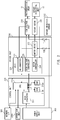
- FIG. 2 and FIG. 3 are explanatory diagrams of a control system for the image forming apparatus 1.
- This control system controls a charging function of charging the surface of the photosensitive drum 11 and a rotation control function of control rotation of the rotary developing unit 13.
- the control system includes a power supply unit 200, a control unit 210, a driver unit 230, a high-voltage unit 240, and a rotary motor 241.
- the power supply unit 200, the control unit 210, the driver unit 230, and the high-voltage unit 240 operate in cooperation with one another to implement the charging function of charging the surface of the photosensitive drum 11.
- the power supply unit 200, the control unit 210, the driver unit 230, and the rotary motor 241 operate in cooperation with one another to implement the rotation control function of control rotation of the rotary developing unit 13.
- Components to be driven by a motor driver 233 may be, for example, a motor for rotating the photosensitive drum 11, a motor for driving a conveyance roller configured to convey paper, or a motor for rotating a polygon mirror included in the laser unit 17, in addition to the rotary motor 241.
- a plurality of functions for forming an image in this manner are formed.
- a board (first board) of the power supply unit 200 includes fuses FU1, FU2, and FU3.
- the control unit 210 includes a DC/DC converter 211, a central processing unit (CPU) 212a, a read only memory (ROM) 212b, and a random access memory (RAM) 212c.
- the driver unit 230 drives the high-voltage unit 240 and the rotary motor 241.
- a board (second board) of the driver unit 230 includes an application specific integrated circuit (ASIC) 231, the motor driver 233, and fuses FU4 and FU5.
- the driver unit 230 includes voltage detectors 303a and 303b, a signal detector 305, and a current detector 306a.
- ASIC application specific integrated circuit
- the driver unit 230 includes voltage detectors 303a and 303b, a signal detector 305, and a current detector 306a.
- Such a control system operates as a power supply, a controller, a signal output device as a signal output unit,
- the power supply unit 200 outputs a power supply voltage of +24 V.
- the power supply unit 200 distributes the power supply voltage to a plurality of voltage supply systems via the fuses FU1 to FU3, to thereby supply current to each component.
- the control unit 210 drops the power supply voltage of +24 V, which has been supplied from the power supply unit 200, to a voltage of 3.3 V by the DC/DC converter 211, to thereby supply current to the CPU 212a and the driver unit 230 (ASIC 231), for example.
- the driver unit 230 supplies the power supply voltage of +24 V, which has been supplied from the power supply unit 200, to the high-voltage unit 240 or the motor driver 233 via the fuses FU4 and FU5.
- the CPU 212a executes a computer program stored in the ROM 212b, to thereby control an operation of each component and execute various kinds of control sequences relating to image formation.
- the RAM 212c is used as a working memory, and stores rewritable data that is required to be stored temporarily or permanently.
- the RAM 212c stores, for example, a high-voltage set value set in the high-voltage unit 240 or drive setting information on a detachable unit.
- the CPU 212a performs serial communication to/from the ASIC 231.
- the CPU 212a uses the serial communication to perform a read/write operation for a register or RAM inside the ASIC 231, to thereby control the operation of the ASIC 231.
- the signal output device in at least one embodiment is implemented by the ASIC 231.
- the ASIC 231 includes function modules such as an AD converter 232 for taking in an analog signal value, a high-voltage controller 235 for controlling the high-voltage unit 240, and a motor controller 234 for controlling the rotary motor 241.
- the ASIC 231 is configured to acquire a set value from the CPU 212a, and set each function module based on the set value. Each function module causes its logic circuit to operate based on the set value, to thereby output a control signal.
- the high-voltage controller 235 outputs a control signal (high-voltage control signal) for controlling the operation of the high-voltage unit 240.
- the motor controller 234 outputs a control signal (motor control signal) for controlling the operation of the motor driver 233.
- the control circuit in at least one embodiment is the high-voltage unit 240 and the motor driver 233.
- the control circuit is a load controller configured to control the operation of the connected load operation device based on a power supply voltage supplied from the power supply and a control signal acquired from the signal output device.
- the motor driver 233 includes a driver integrated circuit (IC) for driving the rotary motor 241.
- the driver IC controls rotation of the rotary motor 241 based on a motor control signal for driving the rotary motor 241.
- the rotary motor 241 is rotated to rotate the rotary developing unit 13 being the load operation device.
- a rotary detection sensor 242 for detecting rotation is provided in the rotary developing unit 13.
- the rotary developing unit 13 is rotated to cause the rotary detection sensor 242 to transmit to the ASIC 231 a detection result indicating detection of rotation.
- the ASIC 231 converts an output signal being an analog signal output from the rotary detection sensor 242 into a digital signal by the AD converter 232, and transmits the digital signal to the CPU 212a.
- the CPU 212a controls the position of the rotary developing unit 13 based on the acquired digital signal.
- the CPU 212a determines that an abnormality has occurred in the position control of the rotary developing unit 13. That is, the rotary detection sensor 242 detects a control abnormality of the rotary developing unit 13 being the load operation device.
- a plurality of sensors (abnormality detectors) configured to detect such a control abnormality are provided in association with a plurality of load operation devices, respectively.
- the CPU 212a stops an image forming operation, and executes failure portion identification processing for identifying a failure portion being a cause of the abnormality.
- the CPU 212a is connected to the operation unit 1000 and a network interface (I/F) 1001.
- the CPU 212a acquires an input signal, for example, an instruction from the operation unit 1000, and displays a screen on the operation unit 1000.
- the CPU 212a performs communication to/from an external device, for example, a computer, by the network I/F 1001 via a predetermined network.
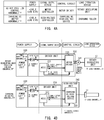
- FIG. 4A and FIG. 4B are explanatory diagrams of the failure portion identification processing in at least one embodiment.
- FIG. 4A is a failure portion identification table storing information (failure portion identification information) indicating portions of the power supply, the signal output device, the control circuit, and the load operation device whose states are to be checked for each type of control abnormality.
- the failure portion identification table is stored in the ROM 212b of the control unit 210.
- the CPU 212a refers to each piece of failure portion identification information of the failure portion occurrence table at the time of occurrence of a control abnormality, and checks the states of components related to the operation abnormality from items on the left side of the table in order, to thereby identify a failure portion.
- FIG. 4B is an explanatory diagram of the failure portion. Identification of the failure portion is executed in order from the power supply, the signal output device, the control circuit, and the load operation device.
- the CPU 212a first starts to check the power supply. As illustrated in FIG. 4A and FIG. 4B , when the abnormality of the position control of the rotary developing unit 13 has occurred, the CPU 212a checks the voltage of +24V_B, which is the input side of the fuse FU5, in order to check the failure portion of the power supply. In order to check the voltage of +24V B, the voltage detector 303a of the driver unit 230 detects whether a value of the voltage of +24V B, which is the input side of the fuse FU5, is equal to or larger than a predetermined value (threshold value). In this case, the threshold value is set to 18 V.
- the result of detection by the voltage detector 303a is transmitted to the CPU 212a via the ASIC 231.
- the CPU 212a checks the failure portion based on the result of detection by the voltage detector 303a.
- the CPU 212a determines that the output of +24V B by the power supply (power supply unit 200) is normal.
- the CPU 212a determines that the output by the power supply (power supply unit 200) is abnormal.
- the CPU 212a When determining that the output by the power supply (power supply unit 200) is abnormal, the CPU 212a confirms that a path (fuse FU3) that outputs the voltage of +24V B of the power supply unit 200 is the failure portion.
- the image forming apparatus 1 does not support replacement of only the fuse parts, and replacement is performed in units of boards. Thus, in this case, the CPU 212a identifies the power supply unit 200 as the failure part (parts to be replaced) (an abnormality of power supply output).
- the voltage detector 303b of the driver unit 230 detects whether the value of the voltage of +24V_B_FU, which is the output side of the fuse FU5, is equal to or larger than a predetermined value (threshold value).
- the voltage detector 303b executes detection processing similarly to the voltage detector 303a, and transmits the detection result to the CPU 212a via the ASIC 231.
- the CPU 212a determines whether the voltage of +24V_B_FU is normal based on the result of detection by the voltage detector 303b. When determining that the voltage of +24V_B_FU is abnormal, the CPU 212a confirms that the fuse FU5 is the failure portion.
- the CPU 212a identifies the driver unit 230 as the failure part (blowout of fuse).
- the CPU 212a determines that the power supply (power supply system of +24V_B in driver unit 230) is normal.
- the CPU 212a checks the failure portion of the signal output device. In order to check the failure portion of the signal output device, the CPU 212a checks a control signal (motor control signal) transmitted from the motor controller 234 of the ASIC 231 to the motor driver 233.
- the motor control signal contains signals such as a rotation direction, speed, or drive mode of the rotary motor 241.
- the CPU 212a In order to check a motor control signal, the CPU 212a first sets the ASIC 231 so that each motor control signal is output at a high level.
- the signal detector 305 of the driver unit 230 compares the value of each motor control signal with a predetermined threshold value. In this case, the threshold value is set to 2.8 V.
- the result of comparison by the signal detector 305 is transmitted to the CPU 212a via the ASIC 231.
- the CPU 212a checks the output state of a motor control signal based on the result of comparison by the signal detector 305. When the comparison result indicates the fact that the value of the motor control signal is equal to or larger than 2.8 V, the CPU 212a determines that the control signal is normal. When the comparison result indicates the fact that the value of the motor control signal is smaller than 2.8 V, the CPU 212a determines that the control signal is abnormal. When determining that the control signal is abnormal, the CPU 212a identifies the motor controller 234 as the failure portion. In this case, the CPU 212a identifies the driver unit 230 as the failure portion (an abnormality of signal output).
- the CPU 212a sets the ASIC 231 so that each motor control signal is output at a low level.
- the signal detector 305 compares the value of each motor control signal with a predetermined threshold value, to thereby check the control signal.
- the threshold value is set to 0.8 V.
- the result of comparison by the signal detector 305 is transmitted to the CPU 212a via the ASIC 231.
- the CPU 212a checks the output state of the motor control signal based on the result of comparison by the signal detector 305. When the comparison result indicates the fact that the value of the motor control signal is smaller than 0.8 V, the CPU 212a determines that the control signal is normal. When the comparison result indicates the fact that the value of the motor control signal is equal to or larger than 0.8 V, the CPU 212a determines that the control signal is abnormal. When determining that the control signal is abnormal, the CPU 212a identifies the motor controller 234 as the failure portion. In this case, the CPU 212a identifies the driver unit 230 as the failure portion (the abnormality of signal output).
- the CPU 212a checks the failure portion of the control circuit. In order to check the failure portion of the control circuit, the CPU 212a checks the output of the motor driver 233.
- the CPU 212a In order to check the output of the motor driver 233, the CPU 212a first sets the motor controller 234 of the ASIC 231 to cause operation of the rotary motor 241.
- the ASIC 231 (motor controller 234) being the signal output device transmits to the motor driver 233 a motor control signal for causing the operation.
- the current detector 306a of the driver unit 230 detects an output current from the control circuit (motor driver 233) under a state in which the power supply voltage and the motor control signal are input to the control circuit (motor driver 233). In order to check whether there is an abnormality of the motor driver 233, the current detector 306a detects whether a value of a current flowing from the motor driver 233 to the rotary motor 241 is equal to or larger than a predetermined value (equal to or larger than threshold value). In this case, the threshold value is set to 100 mA.
- the result of detection by the current detector 306a is transmitted to the CPU 212a via the ASIC 231.
- the CPU 212a checks the failure portion based on the result of detection by the voltage detector 306a.
- the CPU 212a determines that the motor driver 233 is normal.
- the CPU 212a determines that the motor driver 233 is abnormal.
- the CPU 212a identifies the control circuit as the failure portion (an abnormality of the control circuit).
- the CPU 212a determines that the driver unit 230 has failed, whereas when the rotary motor 241 is not in operation, the CPU 212a determines that an actuator has failed (an abnormality of the actuator), and identifies the rotary motor 241 as the failure part.
- the CPU 212a checks the failure portion of the load operation device.
- the CPU 212a executes rotation control of the rotary motor 241 again, to thereby check the load operation device (rotary developing unit 13).
- the CPU 212a checks whether the rotary detection sensor 242 detects rotation of the rotary developing unit 13.
- the CPU 212a acquires the result of detection by the rotary detection sensor 242 via the ASIC 231.
- the CPU 212a determines that the load operation device is abnormal, and identifies the rotary developing unit 13 as the failure portion (an abnormality of the load).
- the rotary developing unit 13 is the failure part.
- the CPU 212a determines that the load operation device is normal. In response to the detection of rotation, the CPU 212a determines that the failure portion cannot be identified.
- the abnormality of the charging DC output is an abnormality that occurs when the primary charging roller 12 charges the surface of the photosensitive drum 11.
- the abnormality of the charging DC output is detected when the surface of the photosensitive drum 11 is not charged to a predetermined voltage value. Whether there is the abnormality of the charging DC output is detected based on a detected value of a current flowing from the high-voltage unit 240 to the photosensitive drum 11 via the primary charging roller 12. This current value is detected by the current detector 306.
- the primary charging roller 12 charges the surface of the photosensitive drum 11 under control by the high-voltage unit 240.
- the CPU 212a When the abnormality of the charging DC output has occurred, the CPU 212a first starts to check a failure of the power supply.
- the CPU 212a checks the voltage of +24V_A, which is the input side of the fuse FU4 installed on the board (second board) of the driver unit 230, to check the failure portion of the power supply.
- the voltage detector 303a of the driver unit 230 detects whether a value of the voltage of +24V_A, which is the input side of the fuse FU4, is equal to or larger than a predetermined value (threshold value). In this case, the threshold value is set to 18 V.
- the result of detection by the voltage detector 303a is transmitted to the CPU 212a via the ASIC 231.
- the CPU 212a checks the failure portion based on the result of detection by the voltage detector 303a.
- the CPU 212a determines that the output by the power supply (power supply unit 200) is normal.
- the CPU 212a determines that the output by the power supply (power supply unit 200) is abnormal.
- the CPU 212a When determining that the output by the power supply (power supply unit 200) is abnormal, the CPU 212a confirms that a path (fuse FU2) that outputs the voltage of +24V A of the power supply unit 200 is the failure portion. In this case, the CPU 212a identifies the power supply unit 200 as the failure part (the abnormality of power supply output).
- the voltage detector 303b of the driver unit 230 detects whether the value of the voltage of +24V_A_FU, which is the output side of the fuse FU4, is equal to or larger than a predetermined value (threshold value).
- the voltage detector 303b executes detection processing similarly to the voltage detector 303a, and transmits the detection result to the CPU 212a via the ASIC 231.
- the CPU 212a determines whether the voltage of +24V_A_FU is normal based on the result of detection by the voltage detector 303b. When determining that the voltage of +24V_A_FU is abnormal, the CPU 212a identifies the fuse FU4 as the failure portion.
- the CPU 212a identifies the driver unit 230 as the failure part (blowout of fuse).
- the CPU 212a determines that the power supply (power supply system of +24V_A in driver unit 230) is normal.
- the CPU 212a checks the failure portion of the signal output device. In order to check the failure portion of the signal output device, the CPU 212a checks a control signal (high-voltage control signal) transmitted from the high-voltage controller 235 of the ASIC 231 to the high-voltage unit 240.
- the high-voltage control signal contains signals such as an output voltage setting signal, or a clock for transformer driving.
- the CPU 212a In order to check a high-voltage control signal, the CPU 212a first sets the ASIC 231 so that each high-voltage control signal is output at a high level.
- the signal detector 305 of the driver unit 230 compares the value of each high-voltage control signal with a predetermined threshold value. In this case, the threshold value is set to 2.8 V.
- the result of comparison by the signal detector 305 is transmitted to the CPU 212a via the ASIC 231.
- the CPU 212a checks the output state of a high-voltage control signal based on the result of comparison by the signal detector 305. When the comparison result indicates the fact that the value of the high-voltage control signal is equal to or larger than 2.8 V, the CPU 212a determines that the control signal is normal. When the comparison result indicates the fact that the value of the high-voltage control signal is smaller than 2.8 V, the CPU 212a determines that the control signal is abnormal. When determining that the control signal is abnormal, the CPU 212a confirms that the high-voltage controller 235 is the failure portion. In this case, the CPU 212a identifies the driver unit 230 as the failure portion (the abnormality of signal output).
- the CPU 212a sets the ASIC 231 so that each high-voltage control signal is output at a low level.
- the signal detector 305 compares the value of each high-voltage control signal with a predetermined threshold value, to thereby check the control signal.
- the threshold value is set to 0.8 V.
- the result of comparison by the signal detector 305 is transmitted to the CPU 212a via the ASIC 231.
- the CPU 212a checks the output state of the high-voltage control signal based on the result of comparison by the signal detector 305. When the comparison result indicates the fact that the value of the high-voltage control signal is smaller than 0.8 V, the CPU 212a determines that the control signal is normal. When the comparison result indicates the fact that the value of the high-voltage control signal is equal to or larger than 0.8 V, the CPU 212a determines that the control signal is abnormal. When determining that the control signal is abnormal, the CPU 212a confirms that the high-voltage controller 235 is the failure portion. In this case, the CPU 212a identifies the driver unit 230 as the failure portion (the abnormality of signal output).
- the CPU 212a checks the failure portion of the control circuit. In order to check the failure portion of the control circuit, the CPU 212a checks the output of a charging DC high-voltage device 220 inside a board (third board) of the high-voltage unit 240.
- the charging DC high-voltage device 220 supplies a high voltage to the primary charging roller 12 so as to charge the photosensitive drum 11.
- the CPU 212a In order to check the output of the charging DC high-voltage device 220, the CPU 212a first sets the high-voltage controller 235 of the ASIC 231 so that the charging DC high-voltage device 220 outputs a predetermined high voltage (-1,000 V in this case).
- the ASIC 231 (high-voltage controller 235) being the signal output device transmits a high-voltage control signal for outputting a predetermined high voltage to the high-voltage unit 240 (charging DC high-voltage device 220).
- the high-voltage unit 240 includes a current detector 306b configured to detect an output current value of the charging DC high-voltage device 220.
- the current detector 306b detects whether the output current value at a time when the charging DC high-voltage device 220 is outputting a high voltage (-1,000 V) in response to the high-voltage control signal is equal to or larger than a predetermined value (equal to or larger than threshold value).
- the threshold value is set to 20 ⁇ A.
- the result of detection by the current detector 306b is transmitted to the CPU 212a via the ASIC 231.
- the CPU 212a checks the output state of the high-voltage control signal based on the result of detection by the voltage detector 306b.
- the CPU 212a determines that a control abnormality of the charging DC high-voltage device 220 has occurred. In this case, the CPU 212a confirms that the charging DC high-voltage device 220 is the failure portion.
- the CPU 212a identifies the high-voltage unit 240 as the failure part (the abnormality of the control circuit).
- the CPU 212a determines that an abnormality due to short-circuit failure inside the photosensitive drum 11 has occurred. In this case, the CPU 212a identifies the photosensitive drum 11 as the failure part (the abnormality of the load).
- FIG. 5A and FIG. 5B are diagrams for illustrating examples of results of processing to be displayed on the operation unit 1000.
- FIG. 5A is a diagram for illustrating an example of display of a processing result in at least one embodiment
- FIG. 5B is a diagram for illustrating an example of display of a processing result in the related art.
- the identified failure part is notified.
- the fact that the power supply unit 200 (first board) is the failure part and is required to be replaced is displayed on the operation unit 1000.
- detailed display of displaying a code or message specifically indicating the failure part is enabled.
- the service engineer can recover the image forming apparatus 1 from the failure state (error state) within a short period of time by replacing the notified failure part without investigating the failure cause. As a result, it is possible to reduce the downtime of the image forming apparatus 1.
- the processing result may be notified to a call center via the network I/F 1001 in addition to display on the operation unit 1000.
- the failure part is notified to the call center via the network I/F 1001 at the time of occurrence of an abnormality, to thereby enable the service engineer to know the failure part without visiting the installation location of the image forming apparatus 1.
- the service engineer can prepare parts for replacement in advance at the time of visiting the installation location, and quickly repair the image forming apparatus 1 to recover the image forming apparatus 1 from the failure state within a short period of time.
- processing for the signal output device is executed after processing for the power supply.
- this order may be opposite. This is because input from the power supply to the control circuit and input from the signal output device to the control circuit are executed in parallel.
- FIG. 6 is a flow chart for illustrating image forming processing including processing of identifying the failure portion.
- the image forming apparatus 1 starts the processing of identifying the failure portion being a cause of the error.
- the CPU 212a waits for input of an instruction to start image formation from the user via the operation unit 1000 or the network I/F 1001 (Step S500: N).
- Step S500: N When an instruction to start image formation is received (Step S500: Y), the CPU 212a starts to form an image in accordance with the instruction.
- the CPU 212a monitors occurrence of an error due to a control abnormality of each component until the image formation is finished (Step S501: N, and Step S509: N).
- the CPU 212a monitors occurrence of an error based on the result of detection by various kinds of sensors installed inside the image forming apparatus 1. When an error has occurred, the CPU 212a performs retry that depends on the type of the error.
- the CPU 212a includes a retry counter configured to count the number of times of retry for each type of an error.
- the CPU 212a clears the number of times of retry for each type of an error stored in the retry counter to all "0" (Step S510).
- Step S501 When an error has occurred during the image formation (Step S501: Y), the CPU 212a stops the image formation (Step S502), and executes the processing of identifying the failure portion (Step S503).
- the rotary developing unit 13 is rotationally driven by the rotary motor 241. Occurrence of this error is detected when the rotary detection sensor 242 has not detected rotation of the rotary developing unit 13 even after a predetermined period of time has elapsed since the rotary motor 241 started control of rotating the rotary developing unit 13.
- the processing of identifying the failure portion is started in response to occurrence of the control abnormality of the rotary developing unit 13. The detailed processing procedure of identification of the failure portion is described later.
- the CPU 212a determines whether the failure portion is identified by the processing of identifying the failure portion (Step S504). When the failure portion is identified (Step S504: Y), as illustrated in FIG. 5A , the CPU 212a finishes the processing by displaying failures parts to be replaced on the operation unit 1000 (Step S508).
- Step S504 the CPU 212a increases the number of times of retry due to an abnormality of a rotary position control by one (Step S505).
- the CPU 212a determines whether the number of times of retry is equal to or larger than a predetermined count (equal to or larger than 3 in this case) (Step S506).
- the CPU 212a resumes the image formation to monitor again whether there is occurrence of an error. That is, the CPU 212a allows the execution of image formation until an error is detected a predetermined number of times. With this process, the image forming processing is executed again.
- Step S506 When the number of times of retry is equal to or larger than the predetermined count (equal to or larger than 3) (Step S506: Y), the CPU 212a determines that the abnormality portion has failed to be identified (Step S507). In this case, the CPU 212a displays the fact that the abnormality portion has failed to be identified on the operation unit 1000, and stops the operation of the apparatus under the error state (Step S508). In this case, similarly to the related art, the service engineer investigates the cause of the error.
- the image forming apparatus 1 executes the image forming processing including the processing of identifying the failure portion, and notifies of a failure part when the failure portion is identified.
- FIG. 7 and FIG. 8 are flow charts for illustrating the processing of identifying the failure portion, which is executed in Step S503.
- FIG. 7 is an illustration of the processing of identifying the failure portion in a case where a control abnormality of the rotary developing unit 13 has occurred.
- FIG. 8 is an illustration of the processing of identifying the failure portion in a case where the abnormality of the charging DC output has occurred.
- the CPU 212a first checks the output state of the power supply (Step S600). When there is no output from the power supply, this means that the power supply has failed.
- Step S601: Y the CPU 212a determines whether the power supply unit 200 (fuse FU3) has failed (Step S602).
- Step S602: Y the CPU 212a identifies the power supply unit 200 as the failure portion (Step S603).
- Step S602: N the CPU 212a identifies the driver unit 230 (fuse FU5) as the failure portion (Step S604).
- Step S601: N the CPU 212a checks the signal output state of the signal output device (Step S605). When an appropriate signal is not output, this means that the signal output device has failed.
- Step S606: Y the CPU 212a identifies the driver unit 230 (motor controller 234) as the failure part because replacement of only the signal output devices is not supported (Step S604).
- Step S606: N the CPU 212a checks the current output state of the control circuit (Step S607). When an appropriate output current is not output, this means that the control circuit has failed.
- Step S608: Y the CPU 212a identifies the driver unit 230 (motor driver 233) as the failure part because the motor driver 233 is mounted on the driver unit 230 (Step S604).
- Step S608: N the CPU 212a checks the operation of the actuator (Step S609).
- Step S610: Y the CPU 212a identifies the rotary motor 241 as the failure part (Step S611).
- Step S612 the CPU 212a controls the load operation device to operate, and checks the operation of the load operation device (Step S612).
- Step S613: Y the CPU 212a identifies the rotary developing unit 13 as the failure part (Step S614).
- Step S613 N
- the CPU 212a determines that the failure portion cannot be identified (Step S615).
- Step S615 "No" is determined in Step S504 of FIG. 6 , and the number of times of retry is increased by one in Step S505.
- Step S620 to Step S626 of FIG. 8 is similar to the processing of Step S601 to Step S606 of FIG. 7 , and thus a description thereof is omitted here.
- Step S626: N the CPU 212a checks the current output state of the control circuit (Step S627). When an appropriate output current is not output, this means that the control circuit has failed.
- Step S628: Y the CPU 212a identifies the high-voltage unit 240 as the failure part because the charging DC high-voltage device 220 configured to output a charging DC is mounted on the high-voltage unit 240 (Step S629).
- Step S630 The processing of identifying the failure portion in the case of the abnormality of the charging DC output skips checking of a failure due to an operation of the load operation device. This is because there is no portion of the load operation device to be determined to have a failure.
- the CPU 212a finishes the processing of identifying the failure portion without checking a failure of a component to be subjected to failure checking.
- the CPU 212a does not redundantly execute processing of identifying the failure portion for a component to be subjected to failure identification other than the identified failure portion.
- the present disclosure can also be applied to other control targets to be driven by the motor, for example.
- the present disclosure can also be applied to, for example, an abnormality of movement of the primary transfer roller.
- identification of a failure portion for a plurality of abnormalities is executed by identifying a failure portion of the power supply, identifying a failure portion of the signal output device, identifying a failure portion of the control circuit, and identifying a failure portion of the load operation device.
- the failure portion is identified by checking the failure in order from the power supply, the signal output device, the control circuit, and the load operation device. With this process, the failure portion can be identified by the same framework for a large number of errors (control abnormalities), and thus a program for identifying the failure portion is inhibited from becoming complex. Further, a memory capacity required for implementation of the function can be reduced, to thereby quickly identify the failure portion at low cost.
- An image forming apparatus (1) includes a plurality of functions for forming an image, which are implemented by a power supply, a signal output unit, a control circuit, and a load operation unit operating in cooperation with one another.
- the load operation unit includes a sensor for detecting an abnormality. When the sensor has detected an abnormality, the image forming apparatus identifies a failure portion being a cause of the abnormality by checking failure portions of the power supply and the signal output unit, checking a failure portion of the control circuit when there is no failure portion in the power supply and the signal output unit, and checking a failure portion of the load operation unit when there is no failure portion in the control circuit.
Landscapes
- Engineering & Computer Science (AREA)
- Multimedia (AREA)
- Signal Processing (AREA)
- Physics & Mathematics (AREA)
- General Physics & Mathematics (AREA)
- Health & Medical Sciences (AREA)
- Biomedical Technology (AREA)
- General Health & Medical Sciences (AREA)
- Microelectronics & Electronic Packaging (AREA)
- Human Computer Interaction (AREA)
- Control Or Security For Electrophotography (AREA)
- Accessory Devices And Overall Control Thereof (AREA)
Abstract
Description
- The present disclosure relates to a technology of identifying, when an abnormality has occurred in operation of an image forming apparatus such as a copying machine or a printer, a failure portion being a cause of the abnormality.
- An image forming apparatus is configured to form an image on a sheet by causing a plurality of components to operate in cooperation with one another. The operation of each component is controlled individually. When the operation control is not finished normally, the image forming apparatus notifies of occurrence of an abnormality by displaying an error code or transmitting an error code to a call center via a network. A service engineer of the image forming apparatus repairs the image forming apparatus based on the error code. In this manner, service support for recovering the operation of the image forming apparatus to a normal state is operated.
- When repairing an image forming apparatus based on an error code, the service engineer appropriately checks a failure of a component related to the error code at the site, and identifies a failure portion required to be repaired. A large amount of time is required for repairing the image forming apparatus, which forces a user to feel inconvenience while the image forming apparatus is being repaired. In Japanese Patent Application Laid-open No.
2005-237046 - A failure of an image forming apparatus may occur not only in a high-voltage power supply but also in each component inside the apparatus. A large number of error codes to be generated in response to a failure are also prepared. A failure portion identification diagnosis program is prepared in association with each error code in some cases. The failure portion identification diagnosis program is used by the service engineer to check a component related to an operation abnormality, to thereby quickly identify a failure portion. However, when a diagnosis program corresponding to each of a large number of error codes is implemented, a storage region for storing software increases, leading to an increase in cost. The present disclosure has a primary object to provide an image forming apparatus configured to quickly identify a failure portion at low cost.
- The present invention in its first aspect provides an image forming apparatus as specified in
claims 1 to 13. - Further features of the present invention will become apparent from the following description of exemplary embodiments (with reference to the attached drawings).
-
-
FIG. 1 is a configuration diagram of an image forming apparatus according to at least one embodiment of the present disclosure. -
FIG. 2 is an explanatory diagram of a control system for the image forming apparatus. -
FIG. 3 is an explanatory diagram of the control system for the image forming apparatus. -
FIG. 4A and FIG. 4B are explanatory diagrams of failure portion identification processing. -
FIG. 5A and FIG. 5B are diagrams for illustrating examples of results of processing to be displayed on an operation portion. -
FIG. 6 is a flow chart for illustrating image forming processing including processing of identifying a failure portion. -
FIG. 7 is a flow chart for illustrating the processing of identifying a failure portion. -
FIG. 8 is a flow chart for illustrating the processing of identifying a failure portion. - An image forming apparatus according to at least one embodiment of the present disclosure is described with reference to the drawings.
-
FIG. 1 is a configuration diagram of an image forming apparatus according to at least one embodiment of the present disclosure. Theimage forming apparatus 1 includes animage reader 2, animage forming unit 3, and anoperation unit 1000. Theimage reader 2 is configured to read a document image from a document D. Theimage forming unit 3 is configured to form an image on a sheet S. Theoperation unit 1000 is a user interface including an input device such as a key button or a touch panel and an output device, for example, a display. Theimage forming apparatus 1 includes a copying function of forming the original image read by theimage reader 2 on the sheet S by theimage forming unit 3. - The
image reader 2 includes, on its upper side, a document table 4 formed of a transparent glass plate and adocument pressing plate 5. The document D is placed at a predetermined position on the document table 4 with an image side thereof facing downward. Thedocument pressing plate 5 presses the document D placed on the document table 4 in a fixed manner. Alamp 6 for irradiating the document D with light, animage processing unit 7, and an optical system includingreflection mirrors image processing unit 7 are installed below the document table 4. Thelamp 6 and the reflection mirrors 8, 9, and 10 move at a predetermined speed to scan the document D. Theimage processing unit 7 generates image data representing a document image based on the optical image of the irradiated document D. - In order to form an image, the
image forming unit 3 includes components such as aphotosensitive drum 11, aprimary charging roller 12, a rotary developingunit 13, anintermediate transfer belt 14, atransfer roller 15, acleaner 16, alaser unit 17, and afixing device 19. Thephotosensitive drum 11 is a photosensitive member having a drum shape, and the surface of thephotosensitive drum 11 is uniformly charged by theprimary charging roller 12. Thelaser unit 17 acquires image data from theimage reader 2, and irradiates thephotosensitive drum 11 having the charged surface with laser light whose light emission is controlled in accordance with this image data. With this process, an electrostatic latent image that depends on the image data is formed on the surface of the photosensitive drum. - The rotary developing
unit 13 causes toners of respective colors of magenta (M), cyan (C), yellow (Y), and black (K) to adhere to the electrostatic latent image formed on the surface of thephotosensitive drum 11, to thereby form a toner image on the surface of thephotosensitive drum 11. The rotary developingunit 13 is a developing device of a rotational development system. The rotary developingunit 13 includes a developingdevice 13K, a developingdevice 13Y, a developingdevice 13M, and a developingdevice 13C, and is rotated by a motor (rotary motor). The developingdevice 13K is configured to develop an image by a toner of black. The developingdevice 13Y is configured to develop an image by a toner of yellow. The developingdevice 13M is configured to develop an image by a toner of magenta. The developingdevice 13C is configured to develop an image by a toner of cyan. - When a monochrome toner image is to be formed on the
photosensitive drum 11, the rotary developingunit 13 develops an image by causing the developingdevice 13K to rotationally move to a development position close to thephotosensitive drum 11. When a full-color toner image is to be formed, the rotary developingunit 13 rotates to arrange the respective developingdevices - The toner image formed on the
photosensitive drum 11 by the rotary developingunit 13 is transferred onto theintermediate transfer belt 14 being a transfer member. Toners that remain on thephotosensitive drum 11 after the transfer are cleaned by thecleaner 16. The toner image transferred onto theintermediate transfer belt 14 is transferred onto the sheet S by thetransfer roller 15. The sheet S is supplied to thetransfer roller 15 from apaper cassette 18 or amanual feed tray 50. Theimage forming apparatus 1 includes a feeding mechanism, for example, a roller, for supplying the sheet S to a conveyance path. - The fixing
device 19 is installed on a downstream side of thetransfer roller 15 with respect to a conveyance direction of the sheet S. The fixingdevice 19 fixes the transferred toner image onto the sheet S. The sheet S on which the toner image is fixed is delivered from the fixingdevice 19 to the outside of theimage forming apparatus 1 via adischarge roller pair 21. - The
image forming apparatus 1 includes afront door 22, which is openable and closable, in order to enable access to consumables such as thephotosensitive drum 11 and therotary developing unit 13 inside theimage forming apparatus 1. Thefront door 22 is opened at the time of repair or inspection of each component described above inside theimage forming apparatus 1 or at the time of replacement of consumables inside theimage forming apparatus 1. Theimage forming apparatus 1 includes a front door open/close sensor 801 for detecting opening/closing of thefront door 22. - The
image forming apparatus 1 includes a paper cassette opening/closing sensor 205 for detecting opening/closing of eachpaper cassette 18, and a paper size detection sensor (not shown) configured to detect a size of the sheet S inside thepaper cassette 18. When thepaper cassette 18 is closed, the paper cassette opening/closing sensor 205 detects this closing. When the paper cassette opening/closing sensor 205 detects closing of thepaper cassette 18, the paper size detection sensor automatically detects the size of the sheet S based on the result of detection. - The
image forming apparatus 1 includes amanual feed sensor 201 configured to detect whether there is a sheet S on themanual feed tray 50. When themanual feed sensor 201 has detected the fact that the sheet S is placed on themanual feed tray 50, theimage forming apparatus 1 displays, on theoperation unit 1000, a screen for urging the user to set the size of the placed sheet S. The user sets the sheet size in accordance with the instruction on the screen, to thereby enable theimage forming apparatus 1 to recognize the size of the sheet S on themanual feed tray 50. - The configuration of the
image forming apparatus 1 is not limited to the above-mentioned configuration, and for example, an image forming apparatus having a well-known configuration in which a plurality of photosensitive drums are arranged along a movement direction of a transfer belt in association with a plurality of color components may be employed. -
FIG. 2 andFIG. 3 are explanatory diagrams of a control system for theimage forming apparatus 1. Now, a description is given of components configured to control thephotosensitive drum 11 and therotary developing unit 13. This control system controls a charging function of charging the surface of thephotosensitive drum 11 and a rotation control function of control rotation of therotary developing unit 13. The control system includes apower supply unit 200, acontrol unit 210, adriver unit 230, a high-voltage unit 240, and arotary motor 241. Thepower supply unit 200, thecontrol unit 210, thedriver unit 230, and the high-voltage unit 240 operate in cooperation with one another to implement the charging function of charging the surface of thephotosensitive drum 11. Thepower supply unit 200, thecontrol unit 210, thedriver unit 230, and therotary motor 241 operate in cooperation with one another to implement the rotation control function of control rotation of therotary developing unit 13. Components to be driven by amotor driver 233 may be, for example, a motor for rotating thephotosensitive drum 11, a motor for driving a conveyance roller configured to convey paper, or a motor for rotating a polygon mirror included in thelaser unit 17, in addition to therotary motor 241. In the control system, a plurality of functions for forming an image in this manner are formed. - A board (first board) of the
power supply unit 200 includes fuses FU1, FU2, and FU3. Thecontrol unit 210 includes a DC/DC converter 211, a central processing unit (CPU) 212a, a read only memory (ROM) 212b, and a random access memory (RAM) 212c. Thedriver unit 230 drives the high-voltage unit 240 and therotary motor 241. To implement this function, a board (second board) of thedriver unit 230 includes an application specific integrated circuit (ASIC) 231, themotor driver 233, and fuses FU4 and FU5. Further, in order to identify a failure portion described later, thedriver unit 230 includesvoltage detectors signal detector 305, and acurrent detector 306a. Such a control system operates as a power supply, a controller, a signal output device as a signal output unit, a control circuit, and a load operation device as a load operation unit. - Now, a description is given of the power supply. The
power supply unit 200 outputs a power supply voltage of +24 V. Thepower supply unit 200 distributes the power supply voltage to a plurality of voltage supply systems via the fuses FU1 to FU3, to thereby supply current to each component. Thecontrol unit 210 drops the power supply voltage of +24 V, which has been supplied from thepower supply unit 200, to a voltage of 3.3 V by the DC/DC converter 211, to thereby supply current to theCPU 212a and the driver unit 230 (ASIC 231), for example. Thedriver unit 230 supplies the power supply voltage of +24 V, which has been supplied from thepower supply unit 200, to the high-voltage unit 240 or themotor driver 233 via the fuses FU4 and FU5. - Now, a description is given of the controller. In the
control unit 210, theCPU 212a executes a computer program stored in theROM 212b, to thereby control an operation of each component and execute various kinds of control sequences relating to image formation. At this time, theRAM 212c is used as a working memory, and stores rewritable data that is required to be stored temporarily or permanently. TheRAM 212c stores, for example, a high-voltage set value set in the high-voltage unit 240 or drive setting information on a detachable unit. TheCPU 212a performs serial communication to/from theASIC 231. TheCPU 212a uses the serial communication to perform a read/write operation for a register or RAM inside theASIC 231, to thereby control the operation of theASIC 231. - Now, a description is given of the signal output device. The signal output device in at least one embodiment is implemented by the
ASIC 231. TheASIC 231 includes function modules such as anAD converter 232 for taking in an analog signal value, a high-voltage controller 235 for controlling the high-voltage unit 240, and amotor controller 234 for controlling therotary motor 241. TheASIC 231 is configured to acquire a set value from theCPU 212a, and set each function module based on the set value. Each function module causes its logic circuit to operate based on the set value, to thereby output a control signal. In at least one embodiment, the high-voltage controller 235 outputs a control signal (high-voltage control signal) for controlling the operation of the high-voltage unit 240. Themotor controller 234 outputs a control signal (motor control signal) for controlling the operation of themotor driver 233. - Now, a description is given of the control circuit. The control circuit in at least one embodiment is the high-
voltage unit 240 and themotor driver 233. The control circuit is a load controller configured to control the operation of the connected load operation device based on a power supply voltage supplied from the power supply and a control signal acquired from the signal output device. - For example, the
motor driver 233 includes a driver integrated circuit (IC) for driving therotary motor 241. The driver IC controls rotation of therotary motor 241 based on a motor control signal for driving therotary motor 241. Therotary motor 241 is rotated to rotate therotary developing unit 13 being the load operation device. Arotary detection sensor 242 for detecting rotation is provided in therotary developing unit 13. Therotary developing unit 13 is rotated to cause therotary detection sensor 242 to transmit to the ASIC 231 a detection result indicating detection of rotation. - The
ASIC 231 converts an output signal being an analog signal output from therotary detection sensor 242 into a digital signal by theAD converter 232, and transmits the digital signal to theCPU 212a. TheCPU 212a controls the position of therotary developing unit 13 based on the acquired digital signal. When the position control is not finished within a predetermined period of time (5 seconds in at least one embodiment), theCPU 212a determines that an abnormality has occurred in the position control of therotary developing unit 13. That is, therotary detection sensor 242 detects a control abnormality of therotary developing unit 13 being the load operation device. A plurality of sensors (abnormality detectors) configured to detect such a control abnormality are provided in association with a plurality of load operation devices, respectively. When occurrence of a control abnormality is determined in this manner, theCPU 212a stops an image forming operation, and executes failure portion identification processing for identifying a failure portion being a cause of the abnormality. - The
CPU 212a is connected to theoperation unit 1000 and a network interface (I/F) 1001. TheCPU 212a acquires an input signal, for example, an instruction from theoperation unit 1000, and displays a screen on theoperation unit 1000. TheCPU 212a performs communication to/from an external device, for example, a computer, by the network I/F 1001 via a predetermined network. -
FIG. 4A and FIG. 4B are explanatory diagrams of the failure portion identification processing in at least one embodiment.FIG. 4A is a failure portion identification table storing information (failure portion identification information) indicating portions of the power supply, the signal output device, the control circuit, and the load operation device whose states are to be checked for each type of control abnormality. The failure portion identification table is stored in theROM 212b of thecontrol unit 210. TheCPU 212a refers to each piece of failure portion identification information of the failure portion occurrence table at the time of occurrence of a control abnormality, and checks the states of components related to the operation abnormality from items on the left side of the table in order, to thereby identify a failure portion. Parts to be replaced of a portion being the failure portion are referred to as "failure parts".FIG. 4B is an explanatory diagram of the failure portion. Identification of the failure portion is executed in order from the power supply, the signal output device, the control circuit, and the load operation device. - Identification of the failure portion at the time of occurrence of an abnormality of a position control of the
rotary developing unit 13 is executed in the following manner. TheCPU 212a first starts to check the power supply. As illustrated inFIG. 4A and FIG. 4B , when the abnormality of the position control of therotary developing unit 13 has occurred, theCPU 212a checks the voltage of +24V_B, which is the input side of the fuse FU5, in order to check the failure portion of the power supply. In order to check the voltage of +24V B, thevoltage detector 303a of thedriver unit 230 detects whether a value of the voltage of +24V B, which is the input side of the fuse FU5, is equal to or larger than a predetermined value (threshold value). In this case, the threshold value is set to 18 V. - The result of detection by the
voltage detector 303a is transmitted to theCPU 212a via theASIC 231. TheCPU 212a checks the failure portion based on the result of detection by thevoltage detector 303a. When the detection result indicates the fact that the value of the voltage of +24V_B is equal to or larger than 18 V, theCPU 212a determines that the output of +24V B by the power supply (power supply unit 200) is normal. When the detection result indicates the fact that the value of the voltage of +24V B is smaller than 18 V, theCPU 212a determines that the output by the power supply (power supply unit 200) is abnormal. When determining that the output by the power supply (power supply unit 200) is abnormal, theCPU 212a confirms that a path (fuse FU3) that outputs the voltage of +24V B of thepower supply unit 200 is the failure portion. Theimage forming apparatus 1 according to at least one embodiment does not support replacement of only the fuse parts, and replacement is performed in units of boards. Thus, in this case, theCPU 212a identifies thepower supply unit 200 as the failure part (parts to be replaced) (an abnormality of power supply output). - When the voltage of +24V_B is normal, the
voltage detector 303b of thedriver unit 230 detects whether the value of the voltage of +24V_B_FU, which is the output side of the fuse FU5, is equal to or larger than a predetermined value (threshold value). Thevoltage detector 303b executes detection processing similarly to thevoltage detector 303a, and transmits the detection result to theCPU 212a via theASIC 231. TheCPU 212a determines whether the voltage of +24V_B_FU is normal based on the result of detection by thevoltage detector 303b. When determining that the voltage of +24V_B_FU is abnormal, theCPU 212a confirms that the fuse FU5 is the failure portion. Similar to thepower supply unit 200, replacement of only the fuse parts is not supported, and replacement is performed in units of boards. Thus, in this case, theCPU 212a identifies thedriver unit 230 as the failure part (blowout of fuse). When determining that the voltages of +24V_B and +24V_B_FU are normal, theCPU 212a determines that the power supply (power supply system of +24V_B in driver unit 230) is normal. - When the power supply system in the
driver unit 230 is normal, theCPU 212a checks the failure portion of the signal output device. In order to check the failure portion of the signal output device, theCPU 212a checks a control signal (motor control signal) transmitted from themotor controller 234 of theASIC 231 to themotor driver 233. The motor control signal contains signals such as a rotation direction, speed, or drive mode of therotary motor 241. - In order to check a motor control signal, the
CPU 212a first sets theASIC 231 so that each motor control signal is output at a high level. Thesignal detector 305 of thedriver unit 230 compares the value of each motor control signal with a predetermined threshold value. In this case, the threshold value is set to 2.8 V. - The result of comparison by the
signal detector 305 is transmitted to theCPU 212a via theASIC 231. TheCPU 212a checks the output state of a motor control signal based on the result of comparison by thesignal detector 305. When the comparison result indicates the fact that the value of the motor control signal is equal to or larger than 2.8 V, theCPU 212a determines that the control signal is normal. When the comparison result indicates the fact that the value of the motor control signal is smaller than 2.8 V, theCPU 212a determines that the control signal is abnormal. When determining that the control signal is abnormal, theCPU 212a identifies themotor controller 234 as the failure portion. In this case, theCPU 212a identifies thedriver unit 230 as the failure portion (an abnormality of signal output). - Next, the
CPU 212a sets theASIC 231 so that each motor control signal is output at a low level. Thesignal detector 305 compares the value of each motor control signal with a predetermined threshold value, to thereby check the control signal. In this case, the threshold value is set to 0.8 V. - The result of comparison by the
signal detector 305 is transmitted to theCPU 212a via theASIC 231. TheCPU 212a checks the output state of the motor control signal based on the result of comparison by thesignal detector 305. When the comparison result indicates the fact that the value of the motor control signal is smaller than 0.8 V, theCPU 212a determines that the control signal is normal. When the comparison result indicates the fact that the value of the motor control signal is equal to or larger than 0.8 V, theCPU 212a determines that the control signal is abnormal. When determining that the control signal is abnormal, theCPU 212a identifies themotor controller 234 as the failure portion. In this case, theCPU 212a identifies thedriver unit 230 as the failure portion (the abnormality of signal output). - When the power supply and the signal output device are normal, the
CPU 212a checks the failure portion of the control circuit. In order to check the failure portion of the control circuit, theCPU 212a checks the output of themotor driver 233. - In order to check the output of the
motor driver 233, theCPU 212a first sets themotor controller 234 of theASIC 231 to cause operation of therotary motor 241. The ASIC 231 (motor controller 234) being the signal output device transmits to the motor driver 233 a motor control signal for causing the operation. - The
current detector 306a of thedriver unit 230 detects an output current from the control circuit (motor driver 233) under a state in which the power supply voltage and the motor control signal are input to the control circuit (motor driver 233). In order to check whether there is an abnormality of themotor driver 233, thecurrent detector 306a detects whether a value of a current flowing from themotor driver 233 to therotary motor 241 is equal to or larger than a predetermined value (equal to or larger than threshold value). In this case, the threshold value is set to 100 mA. - The result of detection by the
current detector 306a is transmitted to theCPU 212a via theASIC 231. TheCPU 212a checks the failure portion based on the result of detection by thevoltage detector 306a. When the detection result indicates the fact that the value of the current flowing through therotary motor 241 is equal to or larger than 100 mA, theCPU 212a determines that themotor driver 233 is normal. When the detection result indicates the fact that the value of the current flowing through therotary motor 241 is smaller than 100 mA, theCPU 212a determines that themotor driver 233 is abnormal. When determining that themotor driver 233 has failed, theCPU 212a identifies the control circuit as the failure portion (an abnormality of the control circuit). - At this time, when the
rotary motor 241 is in operation, theCPU 212a determines that thedriver unit 230 has failed, whereas when therotary motor 241 is not in operation, theCPU 212a determines that an actuator has failed (an abnormality of the actuator), and identifies therotary motor 241 as the failure part. - When the power supply, the signal output device, and the control circuit are normal, the
CPU 212a checks the failure portion of the load operation device. TheCPU 212a executes rotation control of therotary motor 241 again, to thereby check the load operation device (rotary developing unit 13). In order to check the load operation device, theCPU 212a checks whether therotary detection sensor 242 detects rotation of therotary developing unit 13. TheCPU 212a acquires the result of detection by therotary detection sensor 242 via theASIC 231. When therotary detection sensor 242 does not detect rotation of therotary developing unit 13, theCPU 212a determines that the load operation device is abnormal, and identifies therotary developing unit 13 as the failure portion (an abnormality of the load). In this case, therotary developing unit 13 is the failure part. When therotary detection sensor 242 detects rotation of therotary developing unit 13, theCPU 212a determines that the load operation device is normal. In response to the detection of rotation, theCPU 212a determines that the failure portion cannot be identified. - Next, a description is given of processing of identifying the failure portion at a time when an abnormality of a charging DC output is detected. The abnormality of the charging DC output is an abnormality that occurs when the
primary charging roller 12 charges the surface of thephotosensitive drum 11. For example, the abnormality of the charging DC output is detected when the surface of thephotosensitive drum 11 is not charged to a predetermined voltage value. Whether there is the abnormality of the charging DC output is detected based on a detected value of a current flowing from the high-voltage unit 240 to thephotosensitive drum 11 via theprimary charging roller 12. This current value is detected by the current detector 306. Theprimary charging roller 12 charges the surface of thephotosensitive drum 11 under control by the high-voltage unit 240. - When the abnormality of the charging DC output has occurred, the
CPU 212a first starts to check a failure of the power supply. TheCPU 212a checks the voltage of +24V_A, which is the input side of the fuse FU4 installed on the board (second board) of thedriver unit 230, to check the failure portion of the power supply. In order to check the voltage of +24V_A, thevoltage detector 303a of thedriver unit 230 detects whether a value of the voltage of +24V_A, which is the input side of the fuse FU4, is equal to or larger than a predetermined value (threshold value). In this case, the threshold value is set to 18 V. - The result of detection by the
voltage detector 303a is transmitted to theCPU 212a via theASIC 231. TheCPU 212a checks the failure portion based on the result of detection by thevoltage detector 303a. When the detection result indicates the fact that the value of the voltage of +24V_A is equal to or larger than 18 V, theCPU 212a determines that the output by the power supply (power supply unit 200) is normal. When the detection result indicates the fact that the value of the voltage of +24V A is smaller than 18 V, theCPU 212a determines that the output by the power supply (power supply unit 200) is abnormal. When determining that the output by the power supply (power supply unit 200) is abnormal, theCPU 212a confirms that a path (fuse FU2) that outputs the voltage of +24V A of thepower supply unit 200 is the failure portion. In this case, theCPU 212a identifies thepower supply unit 200 as the failure part (the abnormality of power supply output). - When the voltage of +24V_A is normal, the
voltage detector 303b of thedriver unit 230 detects whether the value of the voltage of +24V_A_FU, which is the output side of the fuse FU4, is equal to or larger than a predetermined value (threshold value). Thevoltage detector 303b executes detection processing similarly to thevoltage detector 303a, and transmits the detection result to theCPU 212a via theASIC 231. TheCPU 212a determines whether the voltage of +24V_A_FU is normal based on the result of detection by thevoltage detector 303b. When determining that the voltage of +24V_A_FU is abnormal, theCPU 212a identifies the fuse FU4 as the failure portion. In this case, theCPU 212a identifies thedriver unit 230 as the failure part (blowout of fuse). When determining that the voltages of +24V_A and +24V_A_FU are normal, theCPU 212a determines that the power supply (power supply system of +24V_A in driver unit 230) is normal. - When the power supply system in the
driver unit 230 is normal, theCPU 212a checks the failure portion of the signal output device. In order to check the failure portion of the signal output device, theCPU 212a checks a control signal (high-voltage control signal) transmitted from the high-voltage controller 235 of theASIC 231 to the high-voltage unit 240. The high-voltage control signal contains signals such as an output voltage setting signal, or a clock for transformer driving. - In order to check a high-voltage control signal, the
CPU 212a first sets theASIC 231 so that each high-voltage control signal is output at a high level. Thesignal detector 305 of thedriver unit 230 compares the value of each high-voltage control signal with a predetermined threshold value. In this case, the threshold value is set to 2.8 V. - The result of comparison by the
signal detector 305 is transmitted to theCPU 212a via theASIC 231. TheCPU 212a checks the output state of a high-voltage control signal based on the result of comparison by thesignal detector 305. When the comparison result indicates the fact that the value of the high-voltage control signal is equal to or larger than 2.8 V, theCPU 212a determines that the control signal is normal. When the comparison result indicates the fact that the value of the high-voltage control signal is smaller than 2.8 V, theCPU 212a determines that the control signal is abnormal. When determining that the control signal is abnormal, theCPU 212a confirms that the high-voltage controller 235 is the failure portion. In this case, theCPU 212a identifies thedriver unit 230 as the failure portion (the abnormality of signal output). - Next, the
CPU 212a sets theASIC 231 so that each high-voltage control signal is output at a low level. Thesignal detector 305 compares the value of each high-voltage control signal with a predetermined threshold value, to thereby check the control signal. In this case, the threshold value is set to 0.8 V. - The result of comparison by the
signal detector 305 is transmitted to theCPU 212a via theASIC 231. TheCPU 212a checks the output state of the high-voltage control signal based on the result of comparison by thesignal detector 305. When the comparison result indicates the fact that the value of the high-voltage control signal is smaller than 0.8 V, theCPU 212a determines that the control signal is normal. When the comparison result indicates the fact that the value of the high-voltage control signal is equal to or larger than 0.8 V, theCPU 212a determines that the control signal is abnormal. When determining that the control signal is abnormal, theCPU 212a confirms that the high-voltage controller 235 is the failure portion. In this case, theCPU 212a identifies thedriver unit 230 as the failure portion (the abnormality of signal output). - When the power supply and the signal output device are normal, the
CPU 212a checks the failure portion of the control circuit. In order to check the failure portion of the control circuit, theCPU 212a checks the output of a charging DC high-voltage device 220 inside a board (third board) of the high-voltage unit 240. The charging DC high-voltage device 220 supplies a high voltage to theprimary charging roller 12 so as to charge thephotosensitive drum 11. - In order to check the output of the charging DC high-
voltage device 220, theCPU 212a first sets the high-voltage controller 235 of theASIC 231 so that the charging DC high-voltage device 220 outputs a predetermined high voltage (-1,000 V in this case). The ASIC 231 (high-voltage controller 235) being the signal output device transmits a high-voltage control signal for outputting a predetermined high voltage to the high-voltage unit 240 (charging DC high-voltage device 220). - The high-
voltage unit 240 includes acurrent detector 306b configured to detect an output current value of the charging DC high-voltage device 220. Thecurrent detector 306b detects whether the output current value at a time when the charging DC high-voltage device 220 is outputting a high voltage (-1,000 V) in response to the high-voltage control signal is equal to or larger than a predetermined value (equal to or larger than threshold value). In this case, the threshold value is set to 20 µA. - The result of detection by the
current detector 306b is transmitted to theCPU 212a via theASIC 231. TheCPU 212a checks the output state of the high-voltage control signal based on the result of detection by thevoltage detector 306b. When the detection result indicates the fact that the output voltage value of the charging DC high-voltage device 220 is smaller than 20 µA, theCPU 212a determines that a control abnormality of the charging DC high-voltage device 220 has occurred. In this case, theCPU 212a confirms that the charging DC high-voltage device 220 is the failure portion. TheCPU 212a identifies the high-voltage unit 240 as the failure part (the abnormality of the control circuit). When the detection result indicates the fact that the output current value of the charging DC high-voltage device 220 is equal to or larger than 20 µA, theCPU 212a determines that an abnormality due to short-circuit failure inside thephotosensitive drum 11 has occurred. In this case, theCPU 212a identifies thephotosensitive drum 11 as the failure part (the abnormality of the load). - As described above, processing of identifying the failure portion by a similar diagnosis program is executed for each type of control abnormality. After identification of the failure portion, the
CPU 212a notifies of the processing result. TheCPU 212a notifies of the processing result by displaying the processing result on theoperation unit 1000, for example.FIG. 5A and FIG. 5B are diagrams for illustrating examples of results of processing to be displayed on theoperation unit 1000.FIG. 5A is a diagram for illustrating an example of display of a processing result in at least one embodiment, andFIG. 5B is a diagram for illustrating an example of display of a processing result in the related art. - In
FIG. 5A , the identified failure part is notified. In this example, the fact that the power supply unit 200 (first board) is the failure part and is required to be replaced is displayed on theoperation unit 1000. In this manner, in at least one embodiment, contrary to the related-art simple display (FIG. 5B ) of an error code indicating a control abnormality, detailed display of displaying a code or message specifically indicating the failure part is enabled. With this detailed display, the service engineer can recover theimage forming apparatus 1 from the failure state (error state) within a short period of time by replacing the notified failure part without investigating the failure cause. As a result, it is possible to reduce the downtime of theimage forming apparatus 1. - The processing result may be notified to a call center via the network I/
F 1001 in addition to display on theoperation unit 1000. The failure part is notified to the call center via the network I/F 1001 at the time of occurrence of an abnormality, to thereby enable the service engineer to know the failure part without visiting the installation location of theimage forming apparatus 1. As a result, the service engineer can prepare parts for replacement in advance at the time of visiting the installation location, and quickly repair theimage forming apparatus 1 to recover theimage forming apparatus 1 from the failure state within a short period of time. - In the above-mentioned description of the processing of identifying the failure portion, processing for the signal output device is executed after processing for the power supply. However, this order may be opposite. This is because input from the power supply to the control circuit and input from the signal output device to the control circuit are executed in parallel.
-
FIG. 6 is a flow chart for illustrating image forming processing including processing of identifying the failure portion. When an error (control abnormality) has occurred during the image forming processing, theimage forming apparatus 1 starts the processing of identifying the failure portion being a cause of the error. - The
CPU 212a waits for input of an instruction to start image formation from the user via theoperation unit 1000 or the network I/F 1001 (Step S500: N). When an instruction to start image formation is received (Step S500: Y), theCPU 212a starts to form an image in accordance with the instruction. TheCPU 212a monitors occurrence of an error due to a control abnormality of each component until the image formation is finished (Step S501: N, and Step S509: N). TheCPU 212a monitors occurrence of an error based on the result of detection by various kinds of sensors installed inside theimage forming apparatus 1. When an error has occurred, theCPU 212a performs retry that depends on the type of the error. TheCPU 212a includes a retry counter configured to count the number of times of retry for each type of an error. When the image formation is finished (Step S509: Y), theCPU 212a clears the number of times of retry for each type of an error stored in the retry counter to all "0" (Step S510). When an error has not occurred or when a control abnormality is resolved by retry after an error has occurred, the image forming processing is finished. - When an error has occurred during the image formation (Step S501: Y), the
CPU 212a stops the image formation (Step S502), and executes the processing of identifying the failure portion (Step S503). Now, a description is given of an exemplary case in which an error of not detecting rotation of therotary developing unit 13 has occurred (the abnormality of the position control of the rotary developing unit 13). Therotary developing unit 13 is rotationally driven by therotary motor 241. Occurrence of this error is detected when therotary detection sensor 242 has not detected rotation of therotary developing unit 13 even after a predetermined period of time has elapsed since therotary motor 241 started control of rotating therotary developing unit 13. The processing of identifying the failure portion is started in response to occurrence of the control abnormality of therotary developing unit 13. The detailed processing procedure of identification of the failure portion is described later. - The
CPU 212a determines whether the failure portion is identified by the processing of identifying the failure portion (Step S504). When the failure portion is identified (Step S504: Y), as illustrated inFIG. 5A , theCPU 212a finishes the processing by displaying failures parts to be replaced on the operation unit 1000 (Step S508). - When the failure portion is not identified (Step S504: N), the
CPU 212a increases the number of times of retry due to an abnormality of a rotary position control by one (Step S505). TheCPU 212a determines whether the number of times of retry is equal to or larger than a predetermined count (equal to or larger than 3 in this case) (Step S506). When the number of times of retry is smaller than the predetermined count (smaller than 3) (Step S506: N), theCPU 212a resumes the image formation to monitor again whether there is occurrence of an error. That is, theCPU 212a allows the execution of image formation until an error is detected a predetermined number of times. With this process, the image forming processing is executed again. - When the number of times of retry is equal to or larger than the predetermined count (equal to or larger than 3) (Step S506: Y), the
CPU 212a determines that the abnormality portion has failed to be identified (Step S507). In this case, theCPU 212a displays the fact that the abnormality portion has failed to be identified on theoperation unit 1000, and stops the operation of the apparatus under the error state (Step S508). In this case, similarly to the related art, the service engineer investigates the cause of the error. - As described above, the
image forming apparatus 1 executes the image forming processing including the processing of identifying the failure portion, and notifies of a failure part when the failure portion is identified. -
FIG. 7 andFIG. 8 are flow charts for illustrating the processing of identifying the failure portion, which is executed in Step S503.FIG. 7 is an illustration of the processing of identifying the failure portion in a case where a control abnormality of therotary developing unit 13 has occurred.FIG. 8 is an illustration of the processing of identifying the failure portion in a case where the abnormality of the charging DC output has occurred. - Now, a description is given of the processing of identifying the failure portion in a case where an abnormality has occurred in rotation control of the
rotary developing unit 13. - The
CPU 212a first checks the output state of the power supply (Step S600). When there is no output from the power supply, this means that the power supply has failed. When the power supply has failed (Step S601: Y), theCPU 212a determines whether the power supply unit 200 (fuse FU3) has failed (Step S602). When thepower supply unit 200 has failed (Step S602: Y), theCPU 212a identifies thepower supply unit 200 as the failure portion (Step S603). When thepower supply unit 200 has not failed (Step S602: N), theCPU 212a identifies the driver unit 230 (fuse FU5) as the failure portion (Step S604). - When the power supply has not failed (Step S601: N), the
CPU 212a checks the signal output state of the signal output device (Step S605). When an appropriate signal is not output, this means that the signal output device has failed. When the signal output device has failed (Step S606: Y), theCPU 212a identifies the driver unit 230 (motor controller 234) as the failure part because replacement of only the signal output devices is not supported (Step S604). When the signal output device has not failed (Step S606: N), theCPU 212a checks the current output state of the control circuit (Step S607). When an appropriate output current is not output, this means that the control circuit has failed. When the control circuit has failed (Step S608: Y), theCPU 212a identifies the driver unit 230 (motor driver 233) as the failure part because themotor driver 233 is mounted on the driver unit 230 (Step S604). - When the control circuit has not failed (Step S608: N), the
CPU 212a checks the operation of the actuator (Step S609). When the actuator has failed (Step S610: Y), theCPU 212a identifies therotary motor 241 as the failure part (Step S611). When the actuator has not failed (Step S610: N), theCPU 212a controls the load operation device to operate, and checks the operation of the load operation device (Step S612). When the load operation device has not operated, this means that the load operation device has failed. When the load operation device has failed (Step S613: Y), theCPU 212a identifies therotary developing unit 13 as the failure part (Step S614). When the load operation device has not failed (Step S613: N), theCPU 212a determines that the failure portion cannot be identified (Step S615). As a result, "No" is determined in Step S504 ofFIG. 6 , and the number of times of retry is increased by one in Step S505. - Now, a description is given of the processing of identifying the failure portion in a case where the abnormality of the charging DC output has occurred. The processing of Step S620 to Step S626 of
FIG. 8 is similar to the processing of Step S601 to Step S606 ofFIG. 7 , and thus a description thereof is omitted here. - When the signal output device has not failed (Step S626: N), the
CPU 212a checks the current output state of the control circuit (Step S627). When an appropriate output current is not output, this means that the control circuit has failed. When the control circuit has failed (Step S628: Y), theCPU 212a identifies the high-voltage unit 240 as the failure part because the charging DC high-voltage device 220 configured to output a charging DC is mounted on the high-voltage unit 240 (Step S629). When the control circuit has not failed (Step S628: N), theCPU 212a identifies thephotosensitive drum 11 as the failure part (Step S630). The processing of identifying the failure portion in the case of the abnormality of the charging DC output skips checking of a failure due to an operation of the load operation device. This is because there is no portion of the load operation device to be determined to have a failure. - As illustrated in
FIG. 7 andFIG. 8 , after the failure portion has been identified, theCPU 212a finishes the processing of identifying the failure portion without checking a failure of a component to be subjected to failure checking. Thus, theCPU 212a does not redundantly execute processing of identifying the failure portion for a component to be subjected to failure identification other than the identified failure portion. - In at least one embodiment, a description has been given of the control abnormality of the
rotary developing unit 13, but the present disclosure can also be applied to other control targets to be driven by the motor, for example. In the image forming apparatus including a photosensitive member for each of a plurality of color components and an intermediate transfer member, and having a configuration of moving a primary transfer roller for separating the photosensitive members from the intermediate transfer member, the present disclosure can also be applied to, for example, an abnormality of movement of the primary transfer roller. - In the
image forming apparatus 1 according to at least one embodiment, identification of a failure portion for a plurality of abnormalities is executed by identifying a failure portion of the power supply, identifying a failure portion of the signal output device, identifying a failure portion of the control circuit, and identifying a failure portion of the load operation device. The failure portion is identified by checking the failure in order from the power supply, the signal output device, the control circuit, and the load operation device. With this process, the failure portion can be identified by the same framework for a large number of errors (control abnormalities), and thus a program for identifying the failure portion is inhibited from becoming complex. Further, a memory capacity required for implementation of the function can be reduced, to thereby quickly identify the failure portion at low cost. - While the present invention has been described with reference to exemplary embodiments, it is to be understood that the invention is not limited to the disclosed exemplary embodiments. The scope of the following claims is to be accorded the broadest interpretation so as to encompass all such modifications and equivalent structures and functions.
- An image forming apparatus (1) includes a plurality of functions for forming an image, which are implemented by a power supply, a signal output unit, a control circuit, and a load operation unit operating in cooperation with one another. The load operation unit includes a sensor for detecting an abnormality. When the sensor has detected an abnormality, the image forming apparatus identifies a failure portion being a cause of the abnormality by checking failure portions of the power supply and the signal output unit, checking a failure portion of the control circuit when there is no failure portion in the power supply and the signal output unit, and checking a failure portion of the load operation unit when there is no failure portion in the control circuit.
Claims (13)
- An image forming apparatus, comprising:a power supply means (200) configured to supply a voltage necessary to form an image;a load operation means (241, 11) configured to execute an operation for forming an image;a load control means (233, 240) configured to operate by being supplied with a voltage from the power supply means (200), to thereby control an operation of the load operation means (241, 11);a signal output means (231) configured to operate by being supplied with a voltage from the power supply means (200), to thereby output to the load control means (233, 240) a control signal for controlling an operation to be executed by the load control means (233, 240);a detecting means (242,306b) configured to detect an abnormality of an operation of the load operation means (241, 11); anda control means (210) configured to execute failure portion identification processing of identifying a failure portion which is a cause of an abnormality of an operation of the load operation means (241, 11) by:checking a state of a supply system for the voltage supplied from the power supply means (200) when the detecting means (242, 306b) detects the abnormality;checking a state of the signal output means (231) when there is no failure in the supply system;checking a state of the load control means (233,240) when there is no failure portion in the signal output means (231); andchecking a state of the load operation means (241,11) when there is no failure portion in the load control means (233, 240).
- The image forming apparatus according to claim 1,wherein the load operation means (241, 11) includes a first load (241) and a second load (11),wherein the load control means (233, 240) includes a first load control means (233) configured to control an operation of the first load (241), and a second load control means (240) configured to control an operation of the second load (11),wherein the signal output means (231) includes a first signal output means (234) configured to output a control signal to the first load control means (233), and a second signal output means (235) configured to output a control signal to the second load control means (240), andwherein the detecting means (242, 306b) includes a first abnormality detecting means (242) configured to detect an abnormality of an operation of the first load (241), and a second abnormality detecting means (306b) configured to detect an abnormality of an operation of the second load (11).
- The image forming apparatus according to claim 2, further comprising a storage means (212c) configured to store a table representing information indicating the power supply means (200), the signal output means (231), the load control means (233, 240), and the load operation means (241, 11), the states of which are to be checked for each type of the abnormality,
wherein the control means (210) is configured to execute the failure portion identification processing by referring to the table in accordance with the load operation means (241, 11) for which the abnormality is detected by the detecting means (242). - The image forming apparatus according to any one of claims 1 - 3, further comprising a voltage detecting means (303a, 303b) configured to detect:a voltage value of a supply system to which a voltage is supplied from a first board (200) via a fuse (FU2, FU3), wherein the power supply means (200) is provided on the first board (200); anda voltage value of a supply system to which a voltage is supplied via a fuse (FU4, FU5) which is provided on a second board (230), wherein the signal output means (231) is provided on the second board (230),wherein the control means (210) is configured to identify a failure portion of the supply system based on the voltage values detected by the voltage detecting means (303a,303b).
- The image forming apparatus according to claim 4, wherein the control means (210) is configured to:detect a voltage value of a voltage output from the first board (200) via the fuse (FU2, FU3); anddetect a voltage value of a voltage input via the fuse (FU4, FU5) included in the second board (230), when the detected voltage value is normal.
- The image forming apparatus according to any one of claims 1 - 5, wherein the control means (210) is configured to identify a failure portion relating to the signal output means (231) depending on an output state of the control signal.
- The image forming apparatus according to any one of claims 1 - 6,wherein the load control means (233, 240) is configured to operate the load operation means (241, 11) by supplying one of a voltage and a current to the load operation means (241, 11), andwherein the control means (210) is configured to identify a failure portion relating to the load control means (233, 240) in accordance with one of the voltage and the current supplied from the load control means (233, 240).
- The image forming apparatus according to any one of claims 1 - 7, wherein the control means (210) is configured to avoid, when the failure portion is identified, executing the failure portion identification processing for a part to be subjected to failure identification other than the identified failure portion.
- The image forming apparatus according to any one of claims 1 - 8, wherein the control means (210) is configured to avoid the failure portion identification processing for a part other than a part to be subjected to the failure identification.
- The image forming apparatus according to any one of claims 1 - 9, further comprising a notifying means (212a) configured to give a notification indicating the failure portion identified by the control means (210).
- The image forming apparatus according to claim 10, wherein the notifying means (212a) is configured to give the notification by displaying (1000) the failure portion on a predetermined display.
- The image forming apparatus according to any one of claims 10 - 11, further comprising a network interface (1001) for communicating to/from an outside device,
wherein the notifying means (212a) is configured to give the notification by transmitting the failure portion to the outside device via the network interface (1001). - The image forming apparatus according to any one of claims 1 - 12, wherein the control means (210) is configured to, when the failure portion has failed to be identified, allow execution of image formation until the detecting means (242) detects an abnormality of the load operation means (241, 11) a predetermined number of times.
Applications Claiming Priority (1)
| Application Number | Priority Date | Filing Date | Title |
|---|---|---|---|
| JP2018207948A JP7229727B2 (en) | 2018-11-05 | 2018-11-05 | image forming device |
Publications (2)
| Publication Number | Publication Date |
|---|---|
| EP3647877A1 true EP3647877A1 (en) | 2020-05-06 |
| EP3647877B1 EP3647877B1 (en) | 2024-06-19 |
Family
ID=68424767
Family Applications (1)
| Application Number | Title | Priority Date | Filing Date |
|---|---|---|---|
| EP19206448.3A Active EP3647877B1 (en) | 2018-11-05 | 2019-10-31 | Image forming apparatus |
Country Status (4)
| Country | Link |
|---|---|
| US (1) | US10938997B2 (en) |
| EP (1) | EP3647877B1 (en) |
| JP (1) | JP7229727B2 (en) |
| CN (1) | CN111142347B (en) |
Cited By (1)
| Publication number | Priority date | Publication date | Assignee | Title |
|---|---|---|---|---|
| WO2023075997A1 (en) * | 2021-10-29 | 2023-05-04 | Hewlett-Packard Development Company, L.P. | Status display of image forming apparatus using power input through wired interface |
Families Citing this family (4)
| Publication number | Priority date | Publication date | Assignee | Title |
|---|---|---|---|---|
| US11102358B2 (en) * | 2019-07-01 | 2021-08-24 | Canon Kabushiki Kaisha | Image forming apparatus determining failure when reactivated before preparing a printing operation |
| US11567441B2 (en) * | 2020-11-30 | 2023-01-31 | Canon Kabushiki Kaisha | Image forming apparatus displaying abnormal state of rotary members driven by a motor based on a detected current value |
| JP7593189B2 (en) * | 2021-03-25 | 2024-12-03 | セイコーエプソン株式会社 | Printing device |
| JP7747496B2 (en) * | 2021-11-15 | 2025-10-01 | 東芝テック株式会社 | Image forming apparatus and program |
Citations (3)
| Publication number | Priority date | Publication date | Assignee | Title |
|---|---|---|---|---|
| EP0602343A2 (en) * | 1992-10-23 | 1994-06-22 | Konica Corporation | Abnormality detection circuit for a motor for use in a copier |
| JP2005237046A (en) | 2004-02-17 | 2005-09-02 | Fuji Xerox Co Ltd | Electric equipment and its abnormality determination device |
| US20070280720A1 (en) * | 2006-06-06 | 2007-12-06 | Yoshihisa Kimura | Power supply apparatus and image forming apparatus |
Family Cites Families (8)
| Publication number | Priority date | Publication date | Assignee | Title |
|---|---|---|---|---|
| JPH06141580A (en) * | 1992-10-23 | 1994-05-20 | Konica Corp | Abnormality detecting circuit for motor |
| JP4400072B2 (en) * | 2003-03-14 | 2010-01-20 | 富士ゼロックス株式会社 | Power supply unit that performs control by status monitoring |
| JP2006062129A (en) * | 2004-08-25 | 2006-03-09 | Fuji Xerox Co Ltd | Abnormality detector and detecting method of electronic apparatus |
| JP2006243348A (en) * | 2005-03-03 | 2006-09-14 | Canon Inc | Method for detecting failure location of image forming apparatus |
| JP5230405B2 (en) * | 2008-12-26 | 2013-07-10 | キヤノン株式会社 | Surface potential measuring apparatus and image forming apparatus |
| JP5907768B2 (en) * | 2012-01-25 | 2016-04-26 | シャープ株式会社 | Error detection circuit of image forming apparatus |
| JP2015085661A (en) * | 2013-11-01 | 2015-05-07 | 株式会社沖データ | Printing apparatus, data processing apparatus, and control method for data processing apparatus |
| US20170187321A1 (en) * | 2015-12-28 | 2017-06-29 | Ricoh Company, Ltd. | Motor control device, motor control system, image forming apparatus, conveyance apparatus, and motor control method |
-
2018
- 2018-11-05 JP JP2018207948A patent/JP7229727B2/en active Active
-
2019
- 2019-10-28 US US16/666,228 patent/US10938997B2/en active Active
- 2019-10-31 EP EP19206448.3A patent/EP3647877B1/en active Active
- 2019-10-31 CN CN201911057100.7A patent/CN111142347B/en active Active
Patent Citations (3)
| Publication number | Priority date | Publication date | Assignee | Title |
|---|---|---|---|---|
| EP0602343A2 (en) * | 1992-10-23 | 1994-06-22 | Konica Corporation | Abnormality detection circuit for a motor for use in a copier |
| JP2005237046A (en) | 2004-02-17 | 2005-09-02 | Fuji Xerox Co Ltd | Electric equipment and its abnormality determination device |
| US20070280720A1 (en) * | 2006-06-06 | 2007-12-06 | Yoshihisa Kimura | Power supply apparatus and image forming apparatus |
Cited By (1)
| Publication number | Priority date | Publication date | Assignee | Title |
|---|---|---|---|---|
| WO2023075997A1 (en) * | 2021-10-29 | 2023-05-04 | Hewlett-Packard Development Company, L.P. | Status display of image forming apparatus using power input through wired interface |
Also Published As
| Publication number | Publication date |
|---|---|
| CN111142347A (en) | 2020-05-12 |
| CN111142347B (en) | 2023-03-28 |
| JP7229727B2 (en) | 2023-02-28 |
| US10938997B2 (en) | 2021-03-02 |
| JP2020076792A (en) | 2020-05-21 |
| EP3647877B1 (en) | 2024-06-19 |
| US20200145543A1 (en) | 2020-05-07 |
Similar Documents
| Publication | Publication Date | Title |
|---|---|---|
| EP3647877B1 (en) | Image forming apparatus | |
| JP7683084B2 (en) | Image forming apparatus and control method thereof | |
| US11184487B2 (en) | Image forming apparatus | |
| JP7834463B2 (en) | Image forming apparatus, information processing apparatus | |
| US11245797B2 (en) | Image forming apparatus, malfunction diagnosis method of image forming apparatus, and storage medium | |
| US10996604B2 (en) | Image forming apparatus configured to diagnose failure | |
| US11102358B2 (en) | Image forming apparatus determining failure when reactivated before preparing a printing operation | |
| US11624995B2 (en) | Image forming apparatus that controls failure diagnosis start timimg based on type of error detected and control method therefor | |
| US11146694B2 (en) | Image forming apparatus | |
| US11316985B2 (en) | Image forming apparatus for determining whether a door sensor or an interrupt voltage switch has failed | |
| JP7301520B2 (en) | image forming device | |
| JP2021009225A (en) | Image forming device | |
| JP2021020347A (en) | Image formation apparatus | |
| US10795300B2 (en) | Image forming apparatus | |
| US11188024B2 (en) | Image forming apparatus to which container containing developer is detachably attached | |
| JP2020076840A (en) | Image formation device, and fault site identifying method | |
| JP2020173376A (en) | Image forming apparatus |
Legal Events
| Date | Code | Title | Description |
|---|---|---|---|
| PUAI | Public reference made under article 153(3) epc to a published international application that has entered the european phase |
Free format text: ORIGINAL CODE: 0009012 |
|
| STAA | Information on the status of an ep patent application or granted ep patent |
Free format text: STATUS: THE APPLICATION HAS BEEN PUBLISHED |
|
| AK | Designated contracting states |
Kind code of ref document: A1 Designated state(s): AL AT BE BG CH CY CZ DE DK EE ES FI FR GB GR HR HU IE IS IT LI LT LU LV MC MK MT NL NO PL PT RO RS SE SI SK SM TR |
|
| AX | Request for extension of the european patent |
Extension state: BA ME |
|
| STAA | Information on the status of an ep patent application or granted ep patent |
Free format text: STATUS: REQUEST FOR EXAMINATION WAS MADE |
|
| 17P | Request for examination filed |
Effective date: 20201106 |
|
| RBV | Designated contracting states (corrected) |
Designated state(s): AL AT BE BG CH CY CZ DE DK EE ES FI FR GB GR HR HU IE IS IT LI LT LU LV MC MK MT NL NO PL PT RO RS SE SI SK SM TR |
|
| STAA | Information on the status of an ep patent application or granted ep patent |
Free format text: STATUS: EXAMINATION IS IN PROGRESS |
|
| 17Q | First examination report despatched |
Effective date: 20220207 |
|
| GRAP | Despatch of communication of intention to grant a patent |
Free format text: ORIGINAL CODE: EPIDOSNIGR1 |
|
| STAA | Information on the status of an ep patent application or granted ep patent |
Free format text: STATUS: GRANT OF PATENT IS INTENDED |
|
| INTG | Intention to grant announced |
Effective date: 20240118 |
|
| GRAS | Grant fee paid |
Free format text: ORIGINAL CODE: EPIDOSNIGR3 |
|
| GRAA | (expected) grant |
Free format text: ORIGINAL CODE: 0009210 |
|
| STAA | Information on the status of an ep patent application or granted ep patent |
Free format text: STATUS: THE PATENT HAS BEEN GRANTED |
|
| AK | Designated contracting states |
Kind code of ref document: B1 Designated state(s): AL AT BE BG CH CY CZ DE DK EE ES FI FR GB GR HR HU IE IS IT LI LT LU LV MC MK MT NL NO PL PT RO RS SE SI SK SM TR |
|
| REG | Reference to a national code |
Ref country code: GB Ref legal event code: FG4D |
|
| REG | Reference to a national code |
Ref country code: CH Ref legal event code: EP |
|
| REG | Reference to a national code |
Ref country code: DE Ref legal event code: R096 Ref document number: 602019053827 Country of ref document: DE |
|
| PG25 | Lapsed in a contracting state [announced via postgrant information from national office to epo] |
Ref country code: BG Free format text: LAPSE BECAUSE OF FAILURE TO SUBMIT A TRANSLATION OF THE DESCRIPTION OR TO PAY THE FEE WITHIN THE PRESCRIBED TIME-LIMIT Effective date: 20240619 |
|
| PG25 | Lapsed in a contracting state [announced via postgrant information from national office to epo] |
Ref country code: FI Free format text: LAPSE BECAUSE OF FAILURE TO SUBMIT A TRANSLATION OF THE DESCRIPTION OR TO PAY THE FEE WITHIN THE PRESCRIBED TIME-LIMIT Effective date: 20240619 Ref country code: HR Free format text: LAPSE BECAUSE OF FAILURE TO SUBMIT A TRANSLATION OF THE DESCRIPTION OR TO PAY THE FEE WITHIN THE PRESCRIBED TIME-LIMIT Effective date: 20240619 |
|
| REG | Reference to a national code |
Ref country code: LT Ref legal event code: MG9D |
|
| PG25 | Lapsed in a contracting state [announced via postgrant information from national office to epo] |
Ref country code: GR Free format text: LAPSE BECAUSE OF FAILURE TO SUBMIT A TRANSLATION OF THE DESCRIPTION OR TO PAY THE FEE WITHIN THE PRESCRIBED TIME-LIMIT Effective date: 20240920 |
|
| REG | Reference to a national code |
Ref country code: NL Ref legal event code: MP Effective date: 20240619 |
|
| PG25 | Lapsed in a contracting state [announced via postgrant information from national office to epo] |
Ref country code: LV Free format text: LAPSE BECAUSE OF FAILURE TO SUBMIT A TRANSLATION OF THE DESCRIPTION OR TO PAY THE FEE WITHIN THE PRESCRIBED TIME-LIMIT Effective date: 20240619 |
|
| PG25 | Lapsed in a contracting state [announced via postgrant information from national office to epo] |
Ref country code: NO Free format text: LAPSE BECAUSE OF FAILURE TO SUBMIT A TRANSLATION OF THE DESCRIPTION OR TO PAY THE FEE WITHIN THE PRESCRIBED TIME-LIMIT Effective date: 20240919 Ref country code: LV Free format text: LAPSE BECAUSE OF FAILURE TO SUBMIT A TRANSLATION OF THE DESCRIPTION OR TO PAY THE FEE WITHIN THE PRESCRIBED TIME-LIMIT Effective date: 20240619 Ref country code: HR Free format text: LAPSE BECAUSE OF FAILURE TO SUBMIT A TRANSLATION OF THE DESCRIPTION OR TO PAY THE FEE WITHIN THE PRESCRIBED TIME-LIMIT Effective date: 20240619 Ref country code: GR Free format text: LAPSE BECAUSE OF FAILURE TO SUBMIT A TRANSLATION OF THE DESCRIPTION OR TO PAY THE FEE WITHIN THE PRESCRIBED TIME-LIMIT Effective date: 20240920 Ref country code: FI Free format text: LAPSE BECAUSE OF FAILURE TO SUBMIT A TRANSLATION OF THE DESCRIPTION OR TO PAY THE FEE WITHIN THE PRESCRIBED TIME-LIMIT Effective date: 20240619 Ref country code: BG Free format text: LAPSE BECAUSE OF FAILURE TO SUBMIT A TRANSLATION OF THE DESCRIPTION OR TO PAY THE FEE WITHIN THE PRESCRIBED TIME-LIMIT Effective date: 20240619 Ref country code: RS Free format text: LAPSE BECAUSE OF FAILURE TO SUBMIT A TRANSLATION OF THE DESCRIPTION OR TO PAY THE FEE WITHIN THE PRESCRIBED TIME-LIMIT Effective date: 20240919 |
|
| PG25 | Lapsed in a contracting state [announced via postgrant information from national office to epo] |
Ref country code: NL Free format text: LAPSE BECAUSE OF FAILURE TO SUBMIT A TRANSLATION OF THE DESCRIPTION OR TO PAY THE FEE WITHIN THE PRESCRIBED TIME-LIMIT Effective date: 20240619 |
|
| REG | Reference to a national code |
Ref country code: AT Ref legal event code: MK05 Ref document number: 1696300 Country of ref document: AT Kind code of ref document: T Effective date: 20240619 |
|
| PG25 | Lapsed in a contracting state [announced via postgrant information from national office to epo] |
Ref country code: NL Free format text: LAPSE BECAUSE OF FAILURE TO SUBMIT A TRANSLATION OF THE DESCRIPTION OR TO PAY THE FEE WITHIN THE PRESCRIBED TIME-LIMIT Effective date: 20240619 |
|
| PG25 | Lapsed in a contracting state [announced via postgrant information from national office to epo] |
Ref country code: PT Free format text: LAPSE BECAUSE OF FAILURE TO SUBMIT A TRANSLATION OF THE DESCRIPTION OR TO PAY THE FEE WITHIN THE PRESCRIBED TIME-LIMIT Effective date: 20241021 |
|
| PG25 | Lapsed in a contracting state [announced via postgrant information from national office to epo] |
Ref country code: PT Free format text: LAPSE BECAUSE OF FAILURE TO SUBMIT A TRANSLATION OF THE DESCRIPTION OR TO PAY THE FEE WITHIN THE PRESCRIBED TIME-LIMIT Effective date: 20241021 |
|
| PG25 | Lapsed in a contracting state [announced via postgrant information from national office to epo] |
Ref country code: PL Free format text: LAPSE BECAUSE OF FAILURE TO SUBMIT A TRANSLATION OF THE DESCRIPTION OR TO PAY THE FEE WITHIN THE PRESCRIBED TIME-LIMIT Effective date: 20240619 |
|
| PG25 | Lapsed in a contracting state [announced via postgrant information from national office to epo] |
Ref country code: EE Free format text: LAPSE BECAUSE OF FAILURE TO SUBMIT A TRANSLATION OF THE DESCRIPTION OR TO PAY THE FEE WITHIN THE PRESCRIBED TIME-LIMIT Effective date: 20240619 |
|
| PG25 | Lapsed in a contracting state [announced via postgrant information from national office to epo] |
Ref country code: AT Free format text: LAPSE BECAUSE OF FAILURE TO SUBMIT A TRANSLATION OF THE DESCRIPTION OR TO PAY THE FEE WITHIN THE PRESCRIBED TIME-LIMIT Effective date: 20240619 Ref country code: IS Free format text: LAPSE BECAUSE OF FAILURE TO SUBMIT A TRANSLATION OF THE DESCRIPTION OR TO PAY THE FEE WITHIN THE PRESCRIBED TIME-LIMIT Effective date: 20241019 |
|
| PG25 | Lapsed in a contracting state [announced via postgrant information from national office to epo] |
Ref country code: CZ Free format text: LAPSE BECAUSE OF FAILURE TO SUBMIT A TRANSLATION OF THE DESCRIPTION OR TO PAY THE FEE WITHIN THE PRESCRIBED TIME-LIMIT Effective date: 20240619 |
|
| PG25 | Lapsed in a contracting state [announced via postgrant information from national office to epo] |
Ref country code: SK Free format text: LAPSE BECAUSE OF FAILURE TO SUBMIT A TRANSLATION OF THE DESCRIPTION OR TO PAY THE FEE WITHIN THE PRESCRIBED TIME-LIMIT Effective date: 20240619 Ref country code: RO Free format text: LAPSE BECAUSE OF FAILURE TO SUBMIT A TRANSLATION OF THE DESCRIPTION OR TO PAY THE FEE WITHIN THE PRESCRIBED TIME-LIMIT Effective date: 20240619 |
|
| PG25 | Lapsed in a contracting state [announced via postgrant information from national office to epo] |
Ref country code: ES Free format text: LAPSE BECAUSE OF FAILURE TO SUBMIT A TRANSLATION OF THE DESCRIPTION OR TO PAY THE FEE WITHIN THE PRESCRIBED TIME-LIMIT Effective date: 20240619 Ref country code: SM Free format text: LAPSE BECAUSE OF FAILURE TO SUBMIT A TRANSLATION OF THE DESCRIPTION OR TO PAY THE FEE WITHIN THE PRESCRIBED TIME-LIMIT Effective date: 20240619 |
|
| PG25 | Lapsed in a contracting state [announced via postgrant information from national office to epo] |
Ref country code: SM Free format text: LAPSE BECAUSE OF FAILURE TO SUBMIT A TRANSLATION OF THE DESCRIPTION OR TO PAY THE FEE WITHIN THE PRESCRIBED TIME-LIMIT Effective date: 20240619 Ref country code: SK Free format text: LAPSE BECAUSE OF FAILURE TO SUBMIT A TRANSLATION OF THE DESCRIPTION OR TO PAY THE FEE WITHIN THE PRESCRIBED TIME-LIMIT Effective date: 20240619 Ref country code: RO Free format text: LAPSE BECAUSE OF FAILURE TO SUBMIT A TRANSLATION OF THE DESCRIPTION OR TO PAY THE FEE WITHIN THE PRESCRIBED TIME-LIMIT Effective date: 20240619 Ref country code: PL Free format text: LAPSE BECAUSE OF FAILURE TO SUBMIT A TRANSLATION OF THE DESCRIPTION OR TO PAY THE FEE WITHIN THE PRESCRIBED TIME-LIMIT Effective date: 20240619 Ref country code: IS Free format text: LAPSE BECAUSE OF FAILURE TO SUBMIT A TRANSLATION OF THE DESCRIPTION OR TO PAY THE FEE WITHIN THE PRESCRIBED TIME-LIMIT Effective date: 20241019 Ref country code: ES Free format text: LAPSE BECAUSE OF FAILURE TO SUBMIT A TRANSLATION OF THE DESCRIPTION OR TO PAY THE FEE WITHIN THE PRESCRIBED TIME-LIMIT Effective date: 20240619 Ref country code: EE Free format text: LAPSE BECAUSE OF FAILURE TO SUBMIT A TRANSLATION OF THE DESCRIPTION OR TO PAY THE FEE WITHIN THE PRESCRIBED TIME-LIMIT Effective date: 20240619 Ref country code: CZ Free format text: LAPSE BECAUSE OF FAILURE TO SUBMIT A TRANSLATION OF THE DESCRIPTION OR TO PAY THE FEE WITHIN THE PRESCRIBED TIME-LIMIT Effective date: 20240619 Ref country code: AT Free format text: LAPSE BECAUSE OF FAILURE TO SUBMIT A TRANSLATION OF THE DESCRIPTION OR TO PAY THE FEE WITHIN THE PRESCRIBED TIME-LIMIT Effective date: 20240619 |
|
| PG25 | Lapsed in a contracting state [announced via postgrant information from national office to epo] |
Ref country code: IT Free format text: LAPSE BECAUSE OF FAILURE TO SUBMIT A TRANSLATION OF THE DESCRIPTION OR TO PAY THE FEE WITHIN THE PRESCRIBED TIME-LIMIT Effective date: 20240619 |
|
| REG | Reference to a national code |
Ref country code: DE Ref legal event code: R097 Ref document number: 602019053827 Country of ref document: DE |
|
| PG25 | Lapsed in a contracting state [announced via postgrant information from national office to epo] |
Ref country code: DK Free format text: LAPSE BECAUSE OF FAILURE TO SUBMIT A TRANSLATION OF THE DESCRIPTION OR TO PAY THE FEE WITHIN THE PRESCRIBED TIME-LIMIT Effective date: 20240619 |
|
| PLBE | No opposition filed within time limit |
Free format text: ORIGINAL CODE: 0009261 |
|
| STAA | Information on the status of an ep patent application or granted ep patent |
Free format text: STATUS: NO OPPOSITION FILED WITHIN TIME LIMIT |
|
| 26N | No opposition filed |
Effective date: 20250320 |
|
| REG | Reference to a national code |
Ref country code: CH Ref legal event code: PL |
|
| PG25 | Lapsed in a contracting state [announced via postgrant information from national office to epo] |
Ref country code: MC Free format text: LAPSE BECAUSE OF FAILURE TO SUBMIT A TRANSLATION OF THE DESCRIPTION OR TO PAY THE FEE WITHIN THE PRESCRIBED TIME-LIMIT Effective date: 20240619 |
|
| PG25 | Lapsed in a contracting state [announced via postgrant information from national office to epo] |
Ref country code: BE Free format text: LAPSE BECAUSE OF NON-PAYMENT OF DUE FEES Effective date: 20241031 Ref country code: LU Free format text: LAPSE BECAUSE OF NON-PAYMENT OF DUE FEES Effective date: 20241031 |
|
| PG25 | Lapsed in a contracting state [announced via postgrant information from national office to epo] |
Ref country code: FR Free format text: LAPSE BECAUSE OF NON-PAYMENT OF DUE FEES Effective date: 20241031 |
|
| PG25 | Lapsed in a contracting state [announced via postgrant information from national office to epo] |
Ref country code: CH Free format text: LAPSE BECAUSE OF NON-PAYMENT OF DUE FEES Effective date: 20241031 |
|
| REG | Reference to a national code |
Ref country code: BE Ref legal event code: MM Effective date: 20241031 |
|
| PG25 | Lapsed in a contracting state [announced via postgrant information from national office to epo] |
Ref country code: SE Free format text: LAPSE BECAUSE OF FAILURE TO SUBMIT A TRANSLATION OF THE DESCRIPTION OR TO PAY THE FEE WITHIN THE PRESCRIBED TIME-LIMIT Effective date: 20240619 |
|
| PGFP | Annual fee paid to national office [announced via postgrant information from national office to epo] |
Ref country code: GB Payment date: 20250923 Year of fee payment: 7 |
|
| PG25 | Lapsed in a contracting state [announced via postgrant information from national office to epo] |
Ref country code: IE Free format text: LAPSE BECAUSE OF NON-PAYMENT OF DUE FEES Effective date: 20241031 |
|
| PGFP | Annual fee paid to national office [announced via postgrant information from national office to epo] |
Ref country code: DE Payment date: 20250923 Year of fee payment: 7 |
|
| PG25 | Lapsed in a contracting state [announced via postgrant information from national office to epo] |
Ref country code: HU Free format text: LAPSE BECAUSE OF FAILURE TO SUBMIT A TRANSLATION OF THE DESCRIPTION OR TO PAY THE FEE WITHIN THE PRESCRIBED TIME-LIMIT; INVALID AB INITIO Effective date: 20191031 |
|
| PG25 | Lapsed in a contracting state [announced via postgrant information from national office to epo] |
Ref country code: CY Free format text: LAPSE BECAUSE OF FAILURE TO SUBMIT A TRANSLATION OF THE DESCRIPTION OR TO PAY THE FEE WITHIN THE PRESCRIBED TIME-LIMIT; INVALID AB INITIO Effective date: 20191031 |