EP3647777A1 - Sensor substrate and sensor device - Google Patents
Sensor substrate and sensor device Download PDFInfo
- Publication number
- EP3647777A1 EP3647777A1 EP18823804.2A EP18823804A EP3647777A1 EP 3647777 A1 EP3647777 A1 EP 3647777A1 EP 18823804 A EP18823804 A EP 18823804A EP 3647777 A1 EP3647777 A1 EP 3647777A1
- Authority
- EP
- European Patent Office
- Prior art keywords
- detection electrode
- insulating substrate
- electrodes
- electrode
- detection
- Prior art date
- Legal status (The legal status is an assumption and is not a legal conclusion. Google has not performed a legal analysis and makes no representation as to the accuracy of the status listed.)
- Granted
Links
Images


Classifications
-
- G—PHYSICS
- G01—MEASURING; TESTING
- G01N—INVESTIGATING OR ANALYSING MATERIALS BY DETERMINING THEIR CHEMICAL OR PHYSICAL PROPERTIES
- G01N15/00—Investigating characteristics of particles; Investigating permeability, pore-volume or surface-area of porous materials
- G01N15/06—Investigating concentration of particle suspensions
- G01N15/0606—Investigating concentration of particle suspensions by collecting particles on a support
-
- G—PHYSICS
- G01—MEASURING; TESTING
- G01N—INVESTIGATING OR ANALYSING MATERIALS BY DETERMINING THEIR CHEMICAL OR PHYSICAL PROPERTIES
- G01N27/00—Investigating or analysing materials by the use of electric, electrochemical, or magnetic means
- G01N27/26—Investigating or analysing materials by the use of electric, electrochemical, or magnetic means by investigating electrochemical variables; by using electrolysis or electrophoresis
- G01N27/403—Cells and electrode assemblies
- G01N27/406—Cells and probes with solid electrolytes
- G01N27/407—Cells and probes with solid electrolytes for investigating or analysing gases
- G01N27/4071—Cells and probes with solid electrolytes for investigating or analysing gases using sensor elements of laminated structure
-
- G—PHYSICS
- G01—MEASURING; TESTING
- G01N—INVESTIGATING OR ANALYSING MATERIALS BY DETERMINING THEIR CHEMICAL OR PHYSICAL PROPERTIES
- G01N15/00—Investigating characteristics of particles; Investigating permeability, pore-volume or surface-area of porous materials
- G01N15/06—Investigating concentration of particle suspensions
- G01N15/0656—Investigating concentration of particle suspensions using electric, e.g. electrostatic methods or magnetic methods
-
- G—PHYSICS
- G01—MEASURING; TESTING
- G01N—INVESTIGATING OR ANALYSING MATERIALS BY DETERMINING THEIR CHEMICAL OR PHYSICAL PROPERTIES
- G01N27/00—Investigating or analysing materials by the use of electric, electrochemical, or magnetic means
- G01N27/02—Investigating or analysing materials by the use of electric, electrochemical, or magnetic means by investigating impedance
- G01N27/04—Investigating or analysing materials by the use of electric, electrochemical, or magnetic means by investigating impedance by investigating resistance
-
- G—PHYSICS
- G01—MEASURING; TESTING
- G01N—INVESTIGATING OR ANALYSING MATERIALS BY DETERMINING THEIR CHEMICAL OR PHYSICAL PROPERTIES
- G01N15/00—Investigating characteristics of particles; Investigating permeability, pore-volume or surface-area of porous materials
- G01N2015/0042—Investigating dispersion of solids
- G01N2015/0046—Investigating dispersion of solids in gas, e.g. smoke
-
- Y—GENERAL TAGGING OF NEW TECHNOLOGICAL DEVELOPMENTS; GENERAL TAGGING OF CROSS-SECTIONAL TECHNOLOGIES SPANNING OVER SEVERAL SECTIONS OF THE IPC; TECHNICAL SUBJECTS COVERED BY FORMER USPC CROSS-REFERENCE ART COLLECTIONS [XRACs] AND DIGESTS
- Y02—TECHNOLOGIES OR APPLICATIONS FOR MITIGATION OR ADAPTATION AGAINST CLIMATE CHANGE
- Y02T—CLIMATE CHANGE MITIGATION TECHNOLOGIES RELATED TO TRANSPORTATION
- Y02T10/00—Road transport of goods or passengers
- Y02T10/10—Internal combustion engine [ICE] based vehicles
- Y02T10/40—Engine management systems
Definitions
- the present invention relates to a sensor board including an insulating substrate and electrodes located on the insulating substrate, and a sensor device.
- Automobiles may incorporate a diesel particulate filter (DPF) to collect particulate matter (PM) mainly containing soot in exhaust gas.
- DPF diesel particulate filter
- a known PM detector that serves as a PM detection sensor may include an insulating substrate formed from sintered ceramics, such as sintered aluminum oxide, and detection electrodes located on a surface of the insulating substrate (e.g., Patent Literature 1). The detector detects particulate matter based on a change in the electrical characteristics caused by a detection target, such as PM contained in exhaust gas, adhering between a pair of detection electrodes.
- the PM detector can have lower detection capability for PM after PM has adhered between the detection electrodes.
- a sensor board includes an insulating substrate having an upper surface and a lower surface, a first detection electrode located on the upper surface of the insulating substrate, a second detection electrode located on the lower surface of the insulating substrate, and a heat generator located between the first detection electrode and the second detection electrode inside the insulating substrate and including at least one conductor layer.
- a portion of the insulating substrate between the heat generator and the first detection electrode has the same thickness as a portion of the insulating substrate between the heat generator and the second electrode.
- a sensor device includes the sensor board with the above structure, and a power source that supplies electric power to the first detection electrode and the second detection electrode.
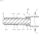
- Fig. 1A is a top view of a sensor board according to an embodiment of the present invention
- Fig. 1B is a cross-sectional view taken along line A-A in Fig. 1A .
- a sensor board 10 is included in a sensor device for detecting, for example, particulate matter (PM) such as soot that may be contained in exhaust gas from a diesel engine vehicle or a gasoline engine vehicle (e.g., installed on a path for exhaust gas from an automobile).
- the sensor board 10 basically includes an insulating substrate 1 having an upper surface and a lower surface, detection electrode 2 located on the upper surface of the insulating substrate 1, second electrode 2 located on the lower surface of the insulating substrate 1, and a heat generator 4 located inside the insulating substrate 1.
- the heat generator 4 includes at least one conductor layer 5 that actually generates heat through resistive heating.
- the conductor layer 5 is located between the first detection electrode 2 and the second detection electrode 3 inside the insulating substrate 1.
- the conductor layer 5 may be simply located between the first detection electrode 2 and the second detection electrode 3 inside the insulating substrate 1 without overlapping the first detection electrode 2 or the second detection electrode 3 in a plan view.
- the first detection electrode 2 include positive electrodes 2a and negative electrodes 2b.
- the second detection electrode 3 include positive electrodes 3a and negative electrodes 3b.
- the first detection electrode 2 or the second detection electrode 3 on the upper or lower surface of the insulating substrate 1 include at least one pair of positive and negative electrodes (with no labels when referred to collectively).
- the first detection electrode 2 and the second detection electrode 3 may be simply referred to as detection electrode or electrode without being distinguished from each other.
- the positive and negative electrodes 2a and 2b may be simply referred to as the first detection electrode 2, and the positive and negative electrode 3a and 3b may be simply referred to as the second detection electrode 3, without being distinguished from each other.
- the first detection electrode 2 and the second detection electrode 3 detect particulate matter in an installation environment of the sensor board 10 by detecting the particulate matter, such as soot, adhering to the insulating substrate 1. More specifically, when detecting such particulate matter, the positive electrodes 2a and 3a and the negative electrodes 2b and 3b change, or for example, their electrical insulation decreases or they are short-circuited. Such changes allow detection of particulate matter in the installation environment of the sensor board 10.
- a short circuit between the positive electrode 2a or 3a and the negative electrode 3a or 3b can be detected by, for example, an external detection circuit connected to the electrodes.
- the environment contains, for example, the exhaust gas from an automobile described above.
- the positive and negative electrodes 2a and 3s as the first detection electrode 2 are located on the upper surface of the insulating substrate 1.
- the positive and negative electrodes 2b and 3b as the second detection electrode 3 are located on the lower surface of the insulating substrate 1.
- the positive electrodes 2a and the negative electrodes 2b as the first detection electrode 2 are interdigitated electrodes that face and interlock each other.
- the positive electrodes 3a and the negative electrodes 2b as the second detection electrode 3 are also interdigitated electrodes that face and interlock each other.
- the first detection electrode 2 has the same line width, interval between adjacent electrodes, and pattern as the second detection electrode 3. This allows particulate matter detection in the same manner on the upper surface and the lower surface of the insulating substrate 1.
- the first detection electrode 2 and the second detection electrode 3 may have different patterns.
- the positive electrodes (2a or 3a) and the negative electrodes (2b or 3b) on the surface on which higher sensitivity for particulate matter is intended may be arranged at smaller intervals than the electrodes on the other surface, depending on the installation environment of the sensor board 1.
- an area including either the first detection electrodes 2 or the second detection electrodes 3 is an effective area in which particulate matter is detectable (an area in which particulate matter may adhere).
- the effective area is to be located in an environment containing, for example, exhaust gas from an automobile, when the sensor board 3 is installed in the environment.
- the first detection electrodes 2 and the second detection electrodes 3 are each connected to a positive electrode or a negative electrode of an external direct current (DC) power source (not shown in Figs. 1A and 1B ) through their terminals 2T.
- the heat generator 4 (described later) is also connected to an external DC power source through its terminals 4T.
- the terminals 2T of the detection electrodes are conductors continuous with the detection electrodes, and are parts of the detection electrodes.
- the terminals 4T of the heat generator are conductors continuous with the heat generator 4, and are parts of the heat generator 4.
- the terminal 2T of the detection electrodes continuous with the positive electrodes 2a or 3a as the detection electrode 2 or 3 is connected to the positive electrode of the DC power source.
- the terminal 2T continuous with the negative electrodes 2b or 3b as the detection electrodes 2 or 3 is connected to the negative electrode of the DC power source.
- the terminals 4T of the heat generator may be connected to the positive electrode and the negative electrode of the same DC power source as above, or to a positive electrode and a negative electrode of another DC power source. This may be determined in accordance with intended conditions such as control, current values, circuit design, and yield.
- the heat generator 4 including at least one conductor layer 5 is located inside the insulating substrate 1.
- two conductor layers 5 are located inside the insulating substrate 1.
- the conductor layers 5 are located between the first detection electrode 2 and the second detection electrode 3.
- being located between the first detection electrode 2 and the second detection electrode 3 refers to being located between the first detection electrode 2 and the second detection electrode 3 in a cross-sectional view of Fig. 1B , for example.
- the conductor layers 5 partially overlap the first detection electrode 2 and the second detection electrode 3 in a plan view.
- the conductor layers 5 may not overlap the first detection electrode 2 or the second detection electrode 3 in a plan view.
- the heat generator 4 is connected to an external DC power source (e.g., a power source of 20 V).
- the heat generating electrode 4 is heated to, for example, about 700 °C to decompose and remove particulate matter adhering to the first detection electrode 2, the second detection electrode 3, and near these electrodes.
- the heat generator 4 generates heat through resistive heating.
- the heat generator 4 includes the conductor layer 5 that actually generates heat.
- connection conductors 6 having a lower electrical resistance extend between the terminals 4T and the conductor layers 5.
- the conductor layers 5 with a smaller line width than the connection conductors 6 have a greater electrical resistance, and thus generate heat through resistive heating with a current supplied from the terminals 4T.
- the heat generator 4 may include a heater (conductor layer 5) located inside the insulating substrate 1 and wires (the terminals 4T and the connection conductor 6) for supplying a current to the heater from the upper and lower surfaces of the insulating substrate 1.
- the conductor layer 5 included in the heat generator 4 is located at the periphery of the insulating substrate 1 in a plan view.
- the conductor layer 5 thus efficiently heats the first detection electrode 2 and the second detection electrode 3 in areas including the above periphery, through which heat can easily escape outside.
- This structure effectively heats, decomposes, and removes particulate matter adhering to the first detection electrode 2, the second detection electrode 3, and near these electrodes.
- the resultant sensor board 10 minimizes the time taken for regeneration, and allows easy fabrication of a highly practical sensor device.
- the upper and lower conductor layers 5 inside the insulating substrate 1 are located adjacent to the upper and lower surfaces of the insulating substrate 1.
- the upper conductor layer 5 is located immediately below the first detection electrode 2 inside the insulating substrate 1.
- the lower conductor layer 5 is located immediately above the second detection electrode 3 inside the insulating substrate 1.
- the upper conductor layer 5 functions as a heater to mainly heat the first detection electrode 2.
- the lower conductor layer 5 functions as a heater to mainly heat the second detection electrode 3.
- a portion of the insulating substrate 1 between the heat generator 4 (conductor layer 5) and the first detection electrode 2 has the same thickness T1 as the thickness T2 of a portion of the insulating substrate 1 between the heat generator 4 (conductor layer 5) and the second electrode 3.
- the thickness T1 of the portion of the insulating substrate 1 between the heat generator 4 (conductor layer 5) and the first detection electrode 2 is the distance between the facing surfaces of the first detection electrode 2 and the conductor layer 2.
- the thickness T2 of the portion of the insulating substrate 1 between the heat generator 4 (conductor layer 5) and the second electrode 3 is the distance between the facing surfaces of the second detection electrode 3 and the conductor layer 2.
- the thickness T1 of the portion of the insulating substrate 1 between the heat generator 4 and the first detection electrode 2 may be referred to as an upper thickness T1
- the thickness T2 of the portion of the insulating substrate 1 between the heat generator 4 and the second electrode 3 may be referred to as a lower thickness T2.
- the upper thickness T1 and the lower thickness T2 may not be precisely the same but may be slightly different due to, for example, accuracy and variations in preparing the insulating substrate 1 and forming the first electrode 2, the second electrode 3, and the conductor layers 5 (described later).
- the thickness of the insulating substrate 1 is about 0.8 to 1.5 mm and the sensor board 10 is fabricated by stacking ceramic green sheets (described later)
- the upper thickness T1 and the lower thickness T2 may differ from each other by about 0.1 to 0.3 mm.
- the insulating substrate 1 which may be a rectangular prism, serves as a base to receive the first detection electrode 2, the second detection electrode 3, and the heat generator 4 in an electrically insulated manner.
- the insulating substrate 1 is formed from sintered ceramics, such as sintered aluminum oxide, sintered aluminum nitride, sintered mullite, sintered glass ceramic, or zirconium ceramic (sintered zirconium oxide).
- the insulating substrate 1 is a stack of multiple insulating layers formed from such sintered ceramics.
- the sensor board 10 can be fabricated by, for example, stacking ceramic green sheets as described below.
- the insulating substrate 1 may be fabricated by, for example, stacking multiple insulating layers formed from sintered aluminum oxide in the manner described below.
- the insulating substrate 1 fabricated in the manner described below includes upper and lower insulating layers sintered with each other at their interface. Thus, no clear boundary may be viewable between these insulating layers.
- a raw material powder such as silicon oxide (SiO 2 ), magnesium oxide (MgO), or manganese oxide (Mn 2 O 3 ) is first added to an aluminum oxide (Al 2 O 3 ) powder as a sintering aid, and an appropriate binder, solvent, and plasticizer are further added to the mixture.
- the mixture is then kneaded to prepare ceramic slurry.
- the ceramic slurry is then shaped into a sheet using a method such as a doctor blade or by calendering to obtain a ceramic green sheet.
- the ceramic green sheet then undergoes punching as appropriate.
- Multiple ceramic green sheets prepared in this manner are stacked on one another as appropriate and fired at high temperatures (about 1300 to 1600 °C). The above processes allow the fabrication of the insulating substrate 1.
- the insulating substrate 1 may include a crystal phase containing alumina and manganese and a glass phase containing manganese.
- the crystal phase may also contain various ceramics, such as mullite, zirconia, aluminum nitride, or glass ceramics, other than alumina.
- the glass phase is an amorphous phase containing at least Mn 2 O 3 , and may further contain at least one oxide of an element selected from the group consisting of Si, Mg, Ca, Sr, B, Nb, Cr, and Co.
- the glass phase may be an amorphous phase containing Mn 2 O 3 , SiO 2 , and MgO.
- the glass phase containing manganese is exposed at the surfaces of the insulating substrate, such as the upper and lower surfaces.
- the insulating substrate 1 has fewer defects that may cause cracks and is thus less likely to break.
- the glass phase having a lower Young's modulus than the crystal phase containing alumina can absorb thermal shock caused by water droplets on the insulating substrate 1, and thus reduces breaks.
- the first and second detection electrodes are formed from a metal material that will not oxidize entirely in an environment containing, for example, a high-temperature air current, such as exhaust gas from an automobile. This allows detection of particulate matter for a long period of time.
- metal materials include easily-passivatable metals and platinum. Electrodes made of platinum are highly resistant to oxidation at high temperatures, and are thus unlikely to oxidize entirely. Electrodes made of an easily-passivatable metal have their exposed surfaces covered with passivation layers, and are thus unlikely to oxidize entirely.
- Examples of easily-passivatable metals include base metal materials that contain at least one element selected from the group consisting of iron, aluminum, nickel, titanium, chromium, and silicon.
- the metal material for the detection electrodes contains, for example, at least one of such base metal materials by at least about 80% by mass.
- the base metal materials do not catalyze decomposition of particulate matter. The use of such materials lowers the likelihood that the adhering particulate matter is decomposed unintentionally and increase the detection accuracy.
- the metal material for the detection electrodes 2 mainly containing at least one of the above base metal materials may further contain at least one of other metal components.
- Such other metal materials may be metal materials that may not easily form passivation layers, and may be other metal materials (e.g. tungsten).
- the first detection electrode 2 and the second detection electrode 3 may be formed in the manner described below.
- a powder of at least one of the above base metal materials is kneaded with an organic solvent and a binder to prepare a metal paste.
- the metal paste is then applied in a predetermined pattern to a main surface and other areas of a ceramic green sheet to be the insulating substrate 1.
- the metal paste is applied by, for example, screen printing.
- the metal paste and the ceramic green sheet are then co-fired.
- the above processes allow the fabrication of the insulating substrate 1 including the detection electrode 2.
- metal materials for forming a passivation layer containing an oxide on the surfaces include a Fe-Ni-Cr-Ti-Al alloy and a MoSi2 metal.
- the thickness of the passivation layer is set to, for example, about 0.1 to 5 ⁇ m.
- the passivation layer with a thickness in the range effectively covers the surfaces of the detection electrodes 3a to 3h, and thus effectively reduces the likelihood that the electrodes oxidize entirely or mostly.
- the first detection electrode 2 and the second detection electrode 3 may have about 90% of their surface areas covered by passivation layers. In other words, 90% or more of the exposed surfaces of the first detection electrode 2 and the second detection electrode 3 may be covered with passivation layers. This structure effectively reduces the likelihood that the detection electrodes oxidize entirely.
- the surfaces of the first detection electrode 2 and the second detection electrode 3 may be entirely covered with passivation layers.
- the exposed surfaces of the detection electrodes may be entirely covered with passivation layers. This structure more effectively reduces the likelihood that the detection electrodes oxidize entirely.
- the terminals 2T of the first detection electrode 2 and the second detection electrodes 3 may also be formed from the same metal material in the same manner as described above.
- the terminals 2T of the first detection electrode 2 and the second detection electrode 3 may also be covered with a plating layer in the same manner as described above.
- the surfaces of the terminals 2T of the first detection electrode 2 and the second detection electrode 3 may be each covered with a metal plating layer by electroplating or electroless plating.
- the metal plating layer is formed from a metal highly resistant to corrosion and easily connectable with a connection member, such as nickel, copper, gold, or silver.
- the metal plating layer includes a nickel plating layer with a thickness of about 0.5 to 10 ⁇ m and a gold plating layer with a thickness of about 0.1 to 3 ⁇ m that are sequentially deposited, or a nickel plating layer with a thickness of about 1 to 10 ⁇ m and a silver plating layer with a thickness of about 0.1 to 1 ⁇ m that are sequentially deposited. These plating layers effectively reduce corrosion at the terminals 2T of the detection electrodes.
- a metal plating layer formed from a metal other than the above metals, such as a palladium plating layer, may be additionally deposited between the above plating layers.
- the conductor layer 5, the connection conductor 6, and the terminals 4T included in the heat generator 4 are formed from, for example, the same metal material and the same manner as the first and second detection electrodes 2 and 3.
- the metal materials for forming the heat generator 4 include materials including iron, titanium, chromium, and silicon with high electrical resistivity, to particularly increase heat generation efficiency.
- the heat generator 4 may mainly contain a metal resistant to oxidation, such as platinum or a Fe-Ni-Cr alloy.
- the above metal material constitutes at least about 80% by mass of the conductor layer 5 in the heat generator, and is a main component of the heat generator 4.
- the heat generators 4 may also contain an inorganic component, such as glass or a ceramic material, other than the metal material.
- the inorganic component adjusts the firing shrinkage that occurs when, for example, the heat generation electrodes 7 are co-fired with the insulating substrate 1.
- connection conductor 6 and the terminals 4T included in the heat generator 4 are electrically connected with each other with a feedthrough conductor (with no labels) extending partially through the insulating substrate 1 in the thickness direction.
- the feedthrough conductor can be a part of the connection conductor 6, and can be formed from the same metal material and the same manner as the connection conductor 6 (described later).
- the first detection electrode 2, the second detection electrode 3, the conductor layer 5, and the connection conductor 6 are formed by preparing a metal paste containing the powder of the above metal material kneaded with an organic solvent and a binder, and applying or embedding, in a predetermined pattern, the metal paste to the surface or into through-holes of the ceramic green sheet to be the insulating substrate 1.
- the through-holes are preliminarily formed by, for example, punching.
- the metal paste is applied or embedded by, for example, screen printing.
- the ceramic green sheet to which the metal paste to be the first detection electrode 2, the second detection electrode 3, the conductor layer 5, and the connection conductor 6 (including the feedthrough conductor) are printed is stacked on other ceramic green sheets as appropriate. The metal paste and the ceramic green sheets are then co-fired.
- the above processes allow the fabrication of the sensor board 10 including the first detection electrode 2, the second detection electrode 3, the conductor layer 5, and the connection conductor 6.
- the upper thickness T1 equal to the lower thickness T2 can be achieved by using the same number of insulating layers with the same layer thickness between the heat generator 4 and the first detection electrode 2 and between the heat generator 4 and the second electrode 3.
- the insulating layers can have varying thicknesses depending on the accuracy in preparing the ceramic green sheets. As described above, the difference in the upper thickness T1 and the lower thickness T2 caused by such variations falls within tolerance.
- the insulating layers between the heat generator 4 and the first detection electrode 2 in the portion with the upper thickness T1 may each have a thickness different from the insulating layers between the heat generator 4 and the second electrode 3 in the portion with the thickness T2.
- the value obtained by multiplying the thickness of each layer and the number of layers for the upper thickness T1 is set the same as the value obtained by multiplying the thickness of each layer and the number of layers for the lower thickness T2.
- Fig. 2 is a cross-sectional view of a sensor board according to another embodiment of the present invention.
- a single conductor layer 5 is located inside an insulating substrate 1.
- a sensor board 10 according to this embodiment includes a heat generator 4 including the single conductor layer 5, a connection section 6, and terminals 4T.
- the structure in this example differs from the structure shown in Figs. 1A and 1B in the heat generator 4, and includes the same other components. The same components as described above will not be described.
- the heat generator 4 including the conductor layer 5 is also located between the first detection electrode 2 and the second detection electrode 3 inside the insulating substrate 1.
- a portion of the insulating substrate 1 between the heat generator 4 and the first detection electrode 2 has the same thickness (upper thickness) T1 as the thickness (lower thickness) T2 of a portion of the insulating substrate between the heat generator 4 and the second electrode 3.
- the single conductor layer 5 supplies heat equally to the upper and lower surfaces of the insulating substrate 1 to heat both the first detection electrode 2 and the second detection electrode 3. This heats and removes particulate matter adhering to the first detection electrode 2, the second detection electrode 3, and near these electrodes.
- the single conductor layer 5 can heat both the first detection electrode 2 and the second detection electrode 3. This structure can reduce the thickness of the sensor board 5. This structure also increases heating efficiency and thus reduces power consumption.
- the upper thickness T1 and the lower thickness T2 are equal to each other.
- This structure allows effective heating on both the upper and lower surfaces of the insulating substrate 1. The structure thus effectively removes particulate matter adhering to the first detection electrode 2, the second detection electrode 3, and near these electrodes.
- the heat generator 4 including the conductor layer 5 immediately below the upper surface of the insulating substrate adjacent to the first detection electrode 2 and the conductor layer 5 immediately above the lower surface of the insulating substrate 1 adjacent to the second detection electrode 3 have the advantageous effects described below.
- the conductor layers 3 can be each located adjacent to the first detection electrode 2 and the second detection electrode 3.
- This structure can effectively heat the adhering particulate matter.
- the structure also allows adjustment of electric power (current value) supplied to the conductor layer 5 adjacent to the first detection electrode 2 and the conductor layer 5 adjacent to the second detection electrode 3.
- the heating conditions current amount
- the structure allows effective use of electric power by the conductor layers 5 in generating heat through resistive heating, thus reducing, for example, the load on automobile batteries for supplying power and improving the performance and usefulness of the automobile including fuel efficiency and durability.
- Fig. 3A is a top view of a sensor board according to another embodiment of the present invention
- Fig. 3B is a cross-sectional view taken along line B-B in Fig. 3A
- conductor layers 5 included in heat generators 4 are located at the periphery of the insulating substrate 1 in a plan view.
- each electrode is columnar, and has its exposed end face functioning as an electrode.
- each heat generator 4 includes the conductor layer 5, a connection section 6, and terminals 4T.
- the structure in this example differs from the structure shown in Figs. 1A and 1B in the arrangement of the conductor layers 4 and the shape of the electrodes, and includes the same other components. The same components as described above will not be described.
- the conductor layers 5 included in the heat generators 4 are located at the periphery of the insulating substrate 1 in a plan view, allowing heat to effectively transfer from the periphery of the insulating substrate 1, through which heat can easily escape outside, toward the middle portion of the insulating substrate 1 in a plan view, thus heating the adhering particulate matter.
- the middle portion of the insulating substrate 1 contains no conductor layer 5 in a plan view. This structure reduces excessive heating of the middle portion with heat generated by the conductor layers 5. This reduces wasteful consumption of power supplied to the conductor layers 5, and allows efficient heating of the adhering particulate matter with less power.
- the conductor layers 5 avoid overlapping the first detection electrode 2 or the second detection electrode 3 in a plan view.
- the conductor layers 5 may be located without overlapping the first detection electrode 2 or the second detection electrode 3.
- This structure also allows heat from the conductor layers 5 to transfer effectively from the periphery of the insulating substrate 1 toward the middle portion in a plan view. This effectively heats and removes particulate matter adhering to the first detection electrode 2, the second detection electrode 3, and near these electrodes.
- the upper thickness T1 and the lower thickness T2 are equal to each other.
- This structure allows effective heating on both the upper and lower surfaces of the insulating substrate 1. The structure thus effectively removes particulate matter adhering to the first detection electrode 2, the second detection electrode 3, and near these electrodes.
- the first detection electrode 2 and the second detection electrode 3 are columnar.
- the columnar electrodes are feedthrough conductors (with no labels for feedthrough conductors) that partially extend through the insulating substrate 1 in the thickness direction.
- the end faces of the feedthrough conductors exposed at the upper and lower surfaces of the insulating substrate 1 practically function as detectors for detecting adhering particulate matter.
- the columnar electrodes include adjacent positive and negative electrodes 2a and 2b and adjacent positive and negative electrodes 3a and 3b.
- the positive electrodes 2a or 3a are connected to a positive electrode of a DC power source.
- the negative electrodes 2b or 3b are connected to a negative electrode of the DC power source.
- the wiring conductors each include, for example, a feedthrough conductor extending from a terminal 2T into the insulating substrate 1 and an inner wire located between insulating layers.
- the feedthrough conductors and the inner wires may be located dispersedly between multiple layers depending on the space allowed for the wiring conductors.
- the positive and negative electrode pairs 2a and 2b or 3a and 3b can be arranged more densely on the insulating substrate 1 than when these electrodes are interdigitated electrodes. Thus, particulate matter can be detected effectively.
- Each pair of positive and negative electrodes 2a and 2b or 3a and 3b may be electrically connected to a different detection circuit.
- This structure can identify a pair of positive electrode 2a or 3a and negative electrode 2b or 3b between which particulate matter has adhered.
- This structure can also detect, for example, a part containing a large amount of particulate matter in the installation environment of the sensor board 10 (e.g., a position in an exhaust pipe for exhaust gas).
- Fig. 4 is a cross-sectional view of a sensor device 20 according to another embodiment of the present invention.
- the sensor device 20 includes a sensor board 10 having any one of the structures described above and power sources P supplying electric power to the first detection electrode 2 and the second detection electrode 3.
- the power sources P are, for example, DC power sources as described above.
- the DC power sources may be storage batteries installed in a device such as an automobile or a facility that discharges a gas containing particulate matter.
- the terminals 2T connected to the first detection electrode 2 and the second detection electrode 3 are connected to lead terminals 11, through which the first and second detection electrodes 2 and 3 are electrically connected to the power sources P.
- the lead terminals 11 are not directly used to detect particulate matter.
- the lead terminals 11 may be formed from any material appropriately selected in accordance with the installation environment, the yield and the economy of the sensor board 10, or other conditions.
- the lead terminals 10a11 are formed from a metal material highly resistant to oxidation such as platinum or gold
- the sensor device 10 including the lead terminals 11 can be highly reliable.
- the lead terminals 11 may also be formed from, for example, an iron based alloy, such as an iron-nickel-cobalt alloy, or copper for economy.
- the lead terminals 10a and 10b including the lead terminals 11 may have the exposed surfaces protected with plating layers, such as gold plating layers.
- the lead terminals 11 are joined to the terminals 2T or other components with, for example, a brazing material (with no labels) such as a silver brazing material (silver-copper brazing material) or a gold brazing material.
- a brazing material such as a silver brazing material (silver-copper brazing material) or a gold brazing material.
- the brazing material may be any material appropriately selected in accordance with various conditions for either manufacturing or using the sensor board 10.
- the terminals 4T included in the heat generators 4 may be electrically connected to power sources with conductive connectors, such as lead terminals (not shown).
- the power sources electrically connected with the terminals 4T of the heat generators 4 may be the same as or different from the power sources P electrically connected with the terminals 2T of the detection electrodes.
- the power sources may be appropriately selected in accordance with, for example, the power amount to be used by the heat generators 4.
- the sensor board and the sensor device according to the embodiments of the present invention are not limited to the structures described above, and may be changed variously within the scope of the present invention.
- the interval between a pair of adjacent positive and negative electrodes 2a and 2b or 3a and 3b as the first or second detection electrode 2 or 3 may differ from the interval between another pair of adjacent positive and negative electrodes 2a and 2b or 3a and 3b.
- the intervals in one portion may be different from the intervals in the other portion.
- the portion with the smaller intervals can detect adhering particulate matter in a low concentration (a low volume percentage in the exhaust gas) with high sensitivity.
- the portion including the larger intervals can detect adhering particulate matter (having a low volume percentage in the exhaust gas) over a longer period of time. More specifically, the sensor board and the sensor device can effectively improve sensitivity and extend the service life.
Landscapes
- Chemical & Material Sciences (AREA)
- Life Sciences & Earth Sciences (AREA)
- Health & Medical Sciences (AREA)
- Physics & Mathematics (AREA)
- Analytical Chemistry (AREA)
- Biochemistry (AREA)
- General Health & Medical Sciences (AREA)
- General Physics & Mathematics (AREA)
- Immunology (AREA)
- Pathology (AREA)
- Dispersion Chemistry (AREA)
- Chemical Kinetics & Catalysis (AREA)
- Electrochemistry (AREA)
- Molecular Biology (AREA)
- Investigating Or Analyzing Materials By The Use Of Electric Means (AREA)
Abstract
Description
- The present invention relates to a sensor board including an insulating substrate and electrodes located on the insulating substrate, and a sensor device.
- Automobiles may incorporate a diesel particulate filter (DPF) to collect particulate matter (PM) mainly containing soot in exhaust gas. To detect, for example, an abnormality of the DPF, a known PM detector that serves as a PM detection sensor may include an insulating substrate formed from sintered ceramics, such as sintered aluminum oxide, and detection electrodes located on a surface of the insulating substrate (e.g., Patent Literature 1). The detector detects particulate matter based on a change in the electrical characteristics caused by a detection target, such as PM contained in exhaust gas, adhering between a pair of detection electrodes.
- The PM detector can have lower detection capability for PM after PM has adhered between the detection electrodes.
- A sensor board according to one aspect of the present invention includes an insulating substrate having an upper surface and a lower surface, a first detection electrode located on the upper surface of the insulating substrate, a second detection electrode located on the lower surface of the insulating substrate, and a heat generator located between the first detection electrode and the second detection electrode inside the insulating substrate and including at least one conductor layer. A portion of the insulating substrate between the heat generator and the first detection electrode has the same thickness as a portion of the insulating substrate between the heat generator and the second electrode.
- A sensor device according to another aspect of the present invention includes the sensor board with the above structure, and a power source that supplies electric power to the first detection electrode and the second detection electrode.
-
-
Fig. 1A is a top view of a sensor board according to an embodiment of the present invention, andFig. 1B is a cross-sectional view taken along line A-A inFig. 1A . -
Fig. 2 is a cross-sectional view of a sensor board according to another embodiment of the present invention. -
Fig. 3A is a top view of a sensor board according to another embodiment of the present invention, andFig. 3B is a cross-sectional view taken along line B-B inFig. 3A . -
Fig. 4 is a cross-sectional view of a sensor device according to another embodiment of the present invention. - A sensor board and a sensor device according to embodiments of the present invention will now be described with reference to the accompanying drawings. The terms upper and lower (e.g., upper surface) herein are for descriptive purposes, and do not intend to limit the directions in, for example, actual use of the sensor board or the sensor device.
-
Fig. 1A is a top view of a sensor board according to an embodiment of the present invention, andFig. 1B is a cross-sectional view taken along line A-A inFig. 1A . - A
sensor board 10 is included in a sensor device for detecting, for example, particulate matter (PM) such as soot that may be contained in exhaust gas from a diesel engine vehicle or a gasoline engine vehicle (e.g., installed on a path for exhaust gas from an automobile). Thesensor board 10 basically includes aninsulating substrate 1 having an upper surface and a lower surface,detection electrode 2 located on the upper surface of theinsulating substrate 1,second electrode 2 located on the lower surface of theinsulating substrate 1, and aheat generator 4 located inside theinsulating substrate 1. Theheat generator 4 includes at least oneconductor layer 5 that actually generates heat through resistive heating. - The
conductor layer 5 is located between thefirst detection electrode 2 and thesecond detection electrode 3 inside theinsulating substrate 1. Theconductor layer 5 may be simply located between thefirst detection electrode 2 and thesecond detection electrode 3 inside theinsulating substrate 1 without overlapping thefirst detection electrode 2 or thesecond detection electrode 3 in a plan view. Thefirst detection electrode 2 includepositive electrodes 2a andnegative electrodes 2b. Thesecond detection electrode 3 includepositive electrodes 3a andnegative electrodes 3b. Thefirst detection electrode 2 or thesecond detection electrode 3 on the upper or lower surface of theinsulating substrate 1 include at least one pair of positive and negative electrodes (with no labels when referred to collectively). In the example described below, thefirst detection electrode 2 and thesecond detection electrode 3 may be simply referred to as detection electrode or electrode without being distinguished from each other. The positive andnegative electrodes first detection electrode 2, and the positive andnegative electrode second detection electrode 3, without being distinguished from each other. - The
first detection electrode 2 and the second detection electrode 3 (on the upper surface and the lower surface of the insulating substrate 1) detect particulate matter in an installation environment of thesensor board 10 by detecting the particulate matter, such as soot, adhering to theinsulating substrate 1. More specifically, when detecting such particulate matter, thepositive electrodes negative electrodes sensor board 10. A short circuit between thepositive electrode negative electrode - The positive and
negative electrodes 2a and 3s as thefirst detection electrode 2 are located on the upper surface of theinsulating substrate 1. The positive andnegative electrodes second detection electrode 3 are located on the lower surface of theinsulating substrate 1. In the example shown inFigs. 1A and 1B , thepositive electrodes 2a and thenegative electrodes 2b as thefirst detection electrode 2 are interdigitated electrodes that face and interlock each other. Thepositive electrodes 3a and thenegative electrodes 2b as thesecond detection electrode 3 are also interdigitated electrodes that face and interlock each other. Thefirst detection electrode 2 has the same line width, interval between adjacent electrodes, and pattern as thesecond detection electrode 3. This allows particulate matter detection in the same manner on the upper surface and the lower surface of theinsulating substrate 1. - The
first detection electrode 2 and thesecond detection electrode 3 may have different patterns. For example, the positive electrodes (2a or 3a) and the negative electrodes (2b or 3b) on the surface on which higher sensitivity for particulate matter is intended may be arranged at smaller intervals than the electrodes on the other surface, depending on the installation environment of thesensor board 1. - In
Figs. 1A and 1B , an area including either thefirst detection electrodes 2 or thesecond detection electrodes 3 is an effective area in which particulate matter is detectable (an area in which particulate matter may adhere). The effective area is to be located in an environment containing, for example, exhaust gas from an automobile, when thesensor board 3 is installed in the environment. - The
first detection electrodes 2 and thesecond detection electrodes 3 are each connected to a positive electrode or a negative electrode of an external direct current (DC) power source (not shown inFigs. 1A and 1B ) through theirterminals 2T. The heat generator 4 (described later) is also connected to an external DC power source through itsterminals 4T. Theterminals 2T of the detection electrodes are conductors continuous with the detection electrodes, and are parts of the detection electrodes. Theterminals 4T of the heat generator are conductors continuous with theheat generator 4, and are parts of theheat generator 4. - The
terminal 2T of the detection electrodes continuous with thepositive electrodes detection electrode terminal 2T continuous with thenegative electrodes detection electrodes terminals 4T of the heat generator may be connected to the positive electrode and the negative electrode of the same DC power source as above, or to a positive electrode and a negative electrode of another DC power source. This may be determined in accordance with intended conditions such as control, current values, circuit design, and yield. - The
heat generator 4 including at least oneconductor layer 5 is located inside the insulatingsubstrate 1. In the example shown inFigs. 1A and 1B , twoconductor layers 5 are located inside the insulatingsubstrate 1. The conductor layers 5 are located between thefirst detection electrode 2 and thesecond detection electrode 3. As described above, being located between thefirst detection electrode 2 and thesecond detection electrode 3 refers to being located between thefirst detection electrode 2 and thesecond detection electrode 3 in a cross-sectional view ofFig. 1B , for example. More specifically, in the example shown inFigs. 1A and 1B , the conductor layers 5 partially overlap thefirst detection electrode 2 and thesecond detection electrode 3 in a plan view. The conductor layers 5 may not overlap thefirst detection electrode 2 or thesecond detection electrode 3 in a plan view. - As described above, the
heat generator 4 is connected to an external DC power source (e.g., a power source of 20 V). Theheat generating electrode 4 is heated to, for example, about 700 °C to decompose and remove particulate matter adhering to thefirst detection electrode 2, thesecond detection electrode 3, and near these electrodes. Theheat generator 4 generates heat through resistive heating. Theheat generator 4 includes theconductor layer 5 that actually generates heat. In the example shown inFigs. 1A and 1B ,connection conductors 6 having a lower electrical resistance extend between theterminals 4T and the conductor layers 5. The conductor layers 5 with a smaller line width than theconnection conductors 6 have a greater electrical resistance, and thus generate heat through resistive heating with a current supplied from theterminals 4T. Theheat generator 4 may include a heater (conductor layer 5) located inside the insulatingsubstrate 1 and wires (theterminals 4T and the connection conductor 6) for supplying a current to the heater from the upper and lower surfaces of the insulatingsubstrate 1. - The
conductor layer 5 included in theheat generator 4 is located at the periphery of the insulatingsubstrate 1 in a plan view. Theconductor layer 5 thus efficiently heats thefirst detection electrode 2 and thesecond detection electrode 3 in areas including the above periphery, through which heat can easily escape outside. This structure effectively heats, decomposes, and removes particulate matter adhering to thefirst detection electrode 2, thesecond detection electrode 3, and near these electrodes. Theresultant sensor board 10 minimizes the time taken for regeneration, and allows easy fabrication of a highly practical sensor device. - In the example shown in
Figs. 1A and 1B , the upper andlower conductor layers 5 inside the insulatingsubstrate 1 are located adjacent to the upper and lower surfaces of the insulatingsubstrate 1. Theupper conductor layer 5 is located immediately below thefirst detection electrode 2 inside the insulatingsubstrate 1. Thelower conductor layer 5 is located immediately above thesecond detection electrode 3 inside the insulatingsubstrate 1. Theupper conductor layer 5 functions as a heater to mainly heat thefirst detection electrode 2. Thelower conductor layer 5 functions as a heater to mainly heat thesecond detection electrode 3. - In the
sensor board 10 according to the embodiment, a portion of the insulatingsubstrate 1 between the heat generator 4 (conductor layer 5) and thefirst detection electrode 2 has the same thickness T1 as the thickness T2 of a portion of the insulatingsubstrate 1 between the heat generator 4 (conductor layer 5) and thesecond electrode 3. In a cross-sectional view shown inFig. 1B , for example, the thickness T1 of the portion of the insulatingsubstrate 1 between the heat generator 4 (conductor layer 5) and thefirst detection electrode 2 is the distance between the facing surfaces of thefirst detection electrode 2 and theconductor layer 2. The thickness T2 of the portion of the insulatingsubstrate 1 between the heat generator 4 (conductor layer 5) and thesecond electrode 3 is the distance between the facing surfaces of thesecond detection electrode 3 and theconductor layer 2. For simplicity, the thickness T1 of the portion of the insulatingsubstrate 1 between theheat generator 4 and thefirst detection electrode 2 may be referred to as an upper thickness T1, and the thickness T2 of the portion of the insulatingsubstrate 1 between theheat generator 4 and thesecond electrode 3 may be referred to as a lower thickness T2. - The upper thickness T1 and the lower thickness T2 may not be precisely the same but may be slightly different due to, for example, accuracy and variations in preparing the insulating
substrate 1 and forming thefirst electrode 2, thesecond electrode 3, and the conductor layers 5 (described later). For example, when the thickness of the insulatingsubstrate 1 is about 0.8 to 1.5 mm and thesensor board 10 is fabricated by stacking ceramic green sheets (described later), the upper thickness T1 and the lower thickness T2 may differ from each other by about 0.1 to 0.3 mm. - The insulating
substrate 1, which may be a rectangular prism, serves as a base to receive thefirst detection electrode 2, thesecond detection electrode 3, and theheat generator 4 in an electrically insulated manner. The insulatingsubstrate 1 is formed from sintered ceramics, such as sintered aluminum oxide, sintered aluminum nitride, sintered mullite, sintered glass ceramic, or zirconium ceramic (sintered zirconium oxide). The insulatingsubstrate 1 is a stack of multiple insulating layers formed from such sintered ceramics. Thesensor board 10 can be fabricated by, for example, stacking ceramic green sheets as described below. - The insulating
substrate 1 may be fabricated by, for example, stacking multiple insulating layers formed from sintered aluminum oxide in the manner described below. The insulatingsubstrate 1 fabricated in the manner described below includes upper and lower insulating layers sintered with each other at their interface. Thus, no clear boundary may be viewable between these insulating layers. - A raw material powder such as silicon oxide (SiO2), magnesium oxide (MgO), or manganese oxide (Mn2O3) is first added to an aluminum oxide (Al2O3) powder as a sintering aid, and an appropriate binder, solvent, and plasticizer are further added to the mixture. The mixture is then kneaded to prepare ceramic slurry. The ceramic slurry is then shaped into a sheet using a method such as a doctor blade or by calendering to obtain a ceramic green sheet. The ceramic green sheet then undergoes punching as appropriate. Multiple ceramic green sheets prepared in this manner are stacked on one another as appropriate and fired at high temperatures (about 1300 to 1600 °C). The above processes allow the fabrication of the insulating
substrate 1. - The insulating
substrate 1 may include a crystal phase containing alumina and manganese and a glass phase containing manganese. The crystal phase may also contain various ceramics, such as mullite, zirconia, aluminum nitride, or glass ceramics, other than alumina. - The glass phase is an amorphous phase containing at least Mn2O3, and may further contain at least one oxide of an element selected from the group consisting of Si, Mg, Ca, Sr, B, Nb, Cr, and Co. The glass phase may be an amorphous phase containing Mn2O3, SiO2, and MgO.
- The glass phase containing manganese is exposed at the surfaces of the insulating substrate, such as the upper and lower surfaces. Thus, the insulating
substrate 1 has fewer defects that may cause cracks and is thus less likely to break. When, for example, the insulatingsubstrate 1 comes in contact with exhaust gas, the glass phase having a lower Young's modulus than the crystal phase containing alumina can absorb thermal shock caused by water droplets on the insulatingsubstrate 1, and thus reduces breaks. - The first and second detection electrodes are formed from a metal material that will not oxidize entirely in an environment containing, for example, a high-temperature air current, such as exhaust gas from an automobile. This allows detection of particulate matter for a long period of time. Examples of such metal materials include easily-passivatable metals and platinum. Electrodes made of platinum are highly resistant to oxidation at high temperatures, and are thus unlikely to oxidize entirely. Electrodes made of an easily-passivatable metal have their exposed surfaces covered with passivation layers, and are thus unlikely to oxidize entirely.
- Examples of easily-passivatable metals include base metal materials that contain at least one element selected from the group consisting of iron, aluminum, nickel, titanium, chromium, and silicon. The metal material for the detection electrodes contains, for example, at least one of such base metal materials by at least about 80% by mass. The base metal materials do not catalyze decomposition of particulate matter. The use of such materials lowers the likelihood that the adhering particulate matter is decomposed unintentionally and increase the detection accuracy.
- The metal material for the
detection electrodes 2 mainly containing at least one of the above base metal materials may further contain at least one of other metal components. Such other metal materials may be metal materials that may not easily form passivation layers, and may be other metal materials (e.g. tungsten). - The
first detection electrode 2 and thesecond detection electrode 3 may be formed in the manner described below. A powder of at least one of the above base metal materials is kneaded with an organic solvent and a binder to prepare a metal paste. The metal paste is then applied in a predetermined pattern to a main surface and other areas of a ceramic green sheet to be the insulatingsubstrate 1. The metal paste is applied by, for example, screen printing. The metal paste and the ceramic green sheet are then co-fired. The above processes allow the fabrication of the insulatingsubstrate 1 including thedetection electrode 2. - More specifically, metal materials for forming a passivation layer containing an oxide on the surfaces include a Fe-Ni-Cr-Ti-Al alloy and a MoSi2 metal. The thickness of the passivation layer is set to, for example, about 0.1 to 5 µm. The passivation layer with a thickness in the range effectively covers the surfaces of the
detection electrodes 3a to 3h, and thus effectively reduces the likelihood that the electrodes oxidize entirely or mostly. - The
first detection electrode 2 and thesecond detection electrode 3 may have about 90% of their surface areas covered by passivation layers. In other words, 90% or more of the exposed surfaces of thefirst detection electrode 2 and thesecond detection electrode 3 may be covered with passivation layers. This structure effectively reduces the likelihood that the detection electrodes oxidize entirely. - The surfaces of the
first detection electrode 2 and thesecond detection electrode 3 may be entirely covered with passivation layers. In other words, the exposed surfaces of the detection electrodes may be entirely covered with passivation layers. This structure more effectively reduces the likelihood that the detection electrodes oxidize entirely. - The
terminals 2T of thefirst detection electrode 2 and thesecond detection electrodes 3 may also be formed from the same metal material in the same manner as described above. Theterminals 2T of thefirst detection electrode 2 and thesecond detection electrode 3 may also be covered with a plating layer in the same manner as described above. - The surfaces of the
terminals 2T of thefirst detection electrode 2 and thesecond detection electrode 3 may be each covered with a metal plating layer by electroplating or electroless plating. The metal plating layer is formed from a metal highly resistant to corrosion and easily connectable with a connection member, such as nickel, copper, gold, or silver. For example, the metal plating layer includes a nickel plating layer with a thickness of about 0.5 to 10 µm and a gold plating layer with a thickness of about 0.1 to 3 µm that are sequentially deposited, or a nickel plating layer with a thickness of about 1 to 10 µm and a silver plating layer with a thickness of about 0.1 to 1 µm that are sequentially deposited. These plating layers effectively reduce corrosion at theterminals 2T of the detection electrodes. A metal plating layer formed from a metal other than the above metals, such as a palladium plating layer, may be additionally deposited between the above plating layers. - The
conductor layer 5, theconnection conductor 6, and theterminals 4T included in theheat generator 4 are formed from, for example, the same metal material and the same manner as the first andsecond detection electrodes conductor layer 5 in particular) include materials including iron, titanium, chromium, and silicon with high electrical resistivity, to particularly increase heat generation efficiency. Theheat generator 4 may mainly contain a metal resistant to oxidation, such as platinum or a Fe-Ni-Cr alloy. - The above metal material constitutes at least about 80% by mass of the
conductor layer 5 in the heat generator, and is a main component of theheat generator 4. Theheat generators 4 may also contain an inorganic component, such as glass or a ceramic material, other than the metal material. The inorganic component adjusts the firing shrinkage that occurs when, for example, the heat generation electrodes 7 are co-fired with the insulatingsubstrate 1. - The
connection conductor 6 and theterminals 4T included in theheat generator 4 are electrically connected with each other with a feedthrough conductor (with no labels) extending partially through the insulatingsubstrate 1 in the thickness direction. The feedthrough conductor can be a part of theconnection conductor 6, and can be formed from the same metal material and the same manner as the connection conductor 6 (described later). - The
first detection electrode 2, thesecond detection electrode 3, theconductor layer 5, and the connection conductor 6 (including the feedthrough conductor) are formed by preparing a metal paste containing the powder of the above metal material kneaded with an organic solvent and a binder, and applying or embedding, in a predetermined pattern, the metal paste to the surface or into through-holes of the ceramic green sheet to be the insulatingsubstrate 1. The through-holes are preliminarily formed by, for example, punching. The metal paste is applied or embedded by, for example, screen printing. The ceramic green sheet to which the metal paste to be thefirst detection electrode 2, thesecond detection electrode 3, theconductor layer 5, and the connection conductor 6 (including the feedthrough conductor) are printed is stacked on other ceramic green sheets as appropriate. The metal paste and the ceramic green sheets are then co-fired. The above processes allow the fabrication of thesensor board 10 including thefirst detection electrode 2, thesecond detection electrode 3, theconductor layer 5, and theconnection conductor 6. - During fabrication, the upper thickness T1 equal to the lower thickness T2 can be achieved by using the same number of insulating layers with the same layer thickness between the
heat generator 4 and thefirst detection electrode 2 and between theheat generator 4 and thesecond electrode 3. In this case, the insulating layers can have varying thicknesses depending on the accuracy in preparing the ceramic green sheets. As described above, the difference in the upper thickness T1 and the lower thickness T2 caused by such variations falls within tolerance. - The insulating layers between the
heat generator 4 and thefirst detection electrode 2 in the portion with the upper thickness T1 may each have a thickness different from the insulating layers between theheat generator 4 and thesecond electrode 3 in the portion with the thickness T2. In this case, the value obtained by multiplying the thickness of each layer and the number of layers for the upper thickness T1 is set the same as the value obtained by multiplying the thickness of each layer and the number of layers for the lower thickness T2. -
Fig. 2 is a cross-sectional view of a sensor board according to another embodiment of the present invention. InFig. 2 , the same components as inFigs. 1A and 1B are given the same reference numerals. In the example shown inFig. 2 , asingle conductor layer 5 is located inside an insulatingsubstrate 1. Asensor board 10 according to this embodiment includes aheat generator 4 including thesingle conductor layer 5, aconnection section 6, andterminals 4T. The structure in this example differs from the structure shown inFigs. 1A and 1B in theheat generator 4, and includes the same other components. The same components as described above will not be described. - In the example shown in
Fig. 2 , theheat generator 4 including theconductor layer 5 is also located between thefirst detection electrode 2 and thesecond detection electrode 3 inside the insulatingsubstrate 1. A portion of the insulatingsubstrate 1 between theheat generator 4 and thefirst detection electrode 2 has the same thickness (upper thickness) T1 as the thickness (lower thickness) T2 of a portion of the insulating substrate between theheat generator 4 and thesecond electrode 3. - In the example shown in
Fig. 2 , thesingle conductor layer 5 supplies heat equally to the upper and lower surfaces of the insulatingsubstrate 1 to heat both thefirst detection electrode 2 and thesecond detection electrode 3. This heats and removes particulate matter adhering to thefirst detection electrode 2, thesecond detection electrode 3, and near these electrodes. In this example, thesingle conductor layer 5 can heat both thefirst detection electrode 2 and thesecond detection electrode 3. This structure can reduce the thickness of thesensor board 5. This structure also increases heating efficiency and thus reduces power consumption. - In the example shown in
Fig. 2 as well, the upper thickness T1 and the lower thickness T2 are equal to each other. This structure allows effective heating on both the upper and lower surfaces of the insulatingsubstrate 1. The structure thus effectively removes particulate matter adhering to thefirst detection electrode 2, thesecond detection electrode 3, and near these electrodes. - As in the embodiment referring to
Figs. 1A and 1B , theheat generator 4 including theconductor layer 5 immediately below the upper surface of the insulating substrate adjacent to thefirst detection electrode 2 and theconductor layer 5 immediately above the lower surface of the insulatingsubstrate 1 adjacent to thesecond detection electrode 3 have the advantageous effects described below. - The conductor layers 3 can be each located adjacent to the
first detection electrode 2 and thesecond detection electrode 3. This structure can effectively heat the adhering particulate matter. The structure also allows adjustment of electric power (current value) supplied to theconductor layer 5 adjacent to thefirst detection electrode 2 and theconductor layer 5 adjacent to thesecond detection electrode 3. When, for example, different amounts of particulate matter adhere to the first andsecond detection electrodes first detection electrode 2 and for thesecond detection electrode 3. The structure allows effective use of electric power by the conductor layers 5 in generating heat through resistive heating, thus reducing, for example, the load on automobile batteries for supplying power and improving the performance and usefulness of the automobile including fuel efficiency and durability. -
Fig. 3A is a top view of a sensor board according to another embodiment of the present invention, andFig. 3B is a cross-sectional view taken along line B-B inFig. 3A . InFig. 2 , the same components as inFigs. 1A and 1B are given the same reference numerals. In the example shown inFigs. 3A and 3B , conductor layers 5 included inheat generators 4 are located at the periphery of the insulatingsubstrate 1 in a plan view. In the example shown inFigs. 3A and 3B , each electrode is columnar, and has its exposed end face functioning as an electrode. In asensor board 10 according to this embodiment, eachheat generator 4 includes theconductor layer 5, aconnection section 6, andterminals 4T. The structure in this example differs from the structure shown inFigs. 1A and 1B in the arrangement of the conductor layers 4 and the shape of the electrodes, and includes the same other components. The same components as described above will not be described. - The conductor layers 5 included in the
heat generators 4 are located at the periphery of the insulatingsubstrate 1 in a plan view, allowing heat to effectively transfer from the periphery of the insulatingsubstrate 1, through which heat can easily escape outside, toward the middle portion of the insulatingsubstrate 1 in a plan view, thus heating the adhering particulate matter. The middle portion of the insulatingsubstrate 1 contains noconductor layer 5 in a plan view. This structure reduces excessive heating of the middle portion with heat generated by the conductor layers 5. This reduces wasteful consumption of power supplied to the conductor layers 5, and allows efficient heating of the adhering particulate matter with less power. - In the example shown in
Figs. 3A and 3B , the conductor layers 5 avoid overlapping thefirst detection electrode 2 or thesecond detection electrode 3 in a plan view. As in this example, the conductor layers 5 may be located without overlapping thefirst detection electrode 2 or thesecond detection electrode 3. This structure also allows heat from the conductor layers 5 to transfer effectively from the periphery of the insulatingsubstrate 1 toward the middle portion in a plan view. This effectively heats and removes particulate matter adhering to thefirst detection electrode 2, thesecond detection electrode 3, and near these electrodes. - In the example shown in
Figs. 3A and 3B as well, the upper thickness T1 and the lower thickness T2 are equal to each other. This structure allows effective heating on both the upper and lower surfaces of the insulatingsubstrate 1. The structure thus effectively removes particulate matter adhering to thefirst detection electrode 2, thesecond detection electrode 3, and near these electrodes. - In the example shown in
Figs. 3A and 3B , thefirst detection electrode 2 and thesecond detection electrode 3 are columnar. The columnar electrodes are feedthrough conductors (with no labels for feedthrough conductors) that partially extend through the insulatingsubstrate 1 in the thickness direction. The end faces of the feedthrough conductors exposed at the upper and lower surfaces of the insulatingsubstrate 1 practically function as detectors for detecting adhering particulate matter. The columnar electrodes include adjacent positive andnegative electrodes negative electrodes positive electrodes negative electrodes - In
Figs. 3A and 3B , the wiring conductors electrically connecting one pair of positive andnegative electrodes terminals 2T of the detection electrodes are shown, and other wiring conductors are not shown for simplifying the drawings. The wiring conductors each include, for example, a feedthrough conductor extending from a terminal 2T into the insulatingsubstrate 1 and an inner wire located between insulating layers. The feedthrough conductors and the inner wires may be located dispersedly between multiple layers depending on the space allowed for the wiring conductors. - When the electrodes are columnar as in this example, the positive and
negative electrode pairs substrate 1 than when these electrodes are interdigitated electrodes. Thus, particulate matter can be detected effectively. Each pair of positive andnegative electrodes positive electrode negative electrode -
Fig. 4 is a cross-sectional view of asensor device 20 according to another embodiment of the present invention. Thesensor device 20 includes asensor board 10 having any one of the structures described above and power sources P supplying electric power to thefirst detection electrode 2 and thesecond detection electrode 3. The power sources P are, for example, DC power sources as described above. The DC power sources may be storage batteries installed in a device such as an automobile or a facility that discharges a gas containing particulate matter. - In the
sensor device 20 according to this embodiment, theterminals 2T connected to thefirst detection electrode 2 and thesecond detection electrode 3 are connected to leadterminals 11, through which the first andsecond detection electrodes - The
lead terminals 11 are not directly used to detect particulate matter. Thus, thelead terminals 11 may be formed from any material appropriately selected in accordance with the installation environment, the yield and the economy of thesensor board 10, or other conditions. When, for example, the lead terminals 10a11 are formed from a metal material highly resistant to oxidation such as platinum or gold, thesensor device 10 including thelead terminals 11 can be highly reliable. Thelead terminals 11 may also be formed from, for example, an iron based alloy, such as an iron-nickel-cobalt alloy, or copper for economy. The lead terminals 10a and 10b including thelead terminals 11 may have the exposed surfaces protected with plating layers, such as gold plating layers. - The
lead terminals 11 are joined to theterminals 2T or other components with, for example, a brazing material (with no labels) such as a silver brazing material (silver-copper brazing material) or a gold brazing material. Similarly to thelead terminals 11, the brazing material may be any material appropriately selected in accordance with various conditions for either manufacturing or using thesensor board 10. - Similarly to the
terminals 2T of the detection electrodes, theterminals 4T included in theheat generators 4 may be electrically connected to power sources with conductive connectors, such as lead terminals (not shown). The power sources electrically connected with theterminals 4T of theheat generators 4 may be the same as or different from the power sources P electrically connected with theterminals 2T of the detection electrodes. The power sources may be appropriately selected in accordance with, for example, the power amount to be used by theheat generators 4. - The sensor board and the sensor device according to the embodiments of the present invention are not limited to the structures described above, and may be changed variously within the scope of the present invention. For example, the interval between a pair of adjacent positive and
negative electrodes second detection electrode negative electrodes -
- 1
- insulating substrate
- 2
- first detection electrode
- 2a
- positive electrode
- 2b
- negative electrode
- 3
- second detection electrode
- 3a
- positive electrode
- 3b
- negative electrode
- 4
- heat generator
- 5
- conductor layer
- 6
- connection conductor
- 10
- sensor board
- 11
- lead terminal
- 20
- sensor device
Claims (4)
- A sensor board, comprising:an insulating substrate having an upper surface and a lower surface;a first detection electrode located on the upper surface of the insulating substrate;a second detection electrode located on the lower surface of the insulating substrate; anda heat generator located between the first detection electrode and the second detection electrode inside the insulating substrate, the heat generator including at least one conductor layer,wherein a portion of the insulating substrate between the heat generator and the first detection electrode has the same thickness as a portion of the insulating substrate between the heat generator and the second electrode.
- The sensor board according to claim 1, wherein
the heat generator includes a conductor layer located adjacent to the first detection electrode and immediately below the upper surface of the insulating substrate, and a conductor layer located adjacent to the second detection electrode and immediately above the lower surface of the insulating substrate. - The sensor board according to claim 1 or claim 2, wherein
the conductor layer included in the heat generator is located at a periphery of the insulating substrate in a plan view. - A sensor device, comprising:the sensor board according to any one of claims 1 to 3; anda power source configured to supply electric power to the first detection electrode and the second detection electrode.
Applications Claiming Priority (2)
| Application Number | Priority Date | Filing Date | Title |
|---|---|---|---|
| JP2017125161 | 2017-06-27 | ||
| PCT/JP2018/016610 WO2019003612A1 (en) | 2017-06-27 | 2018-04-24 | Sensor substrate and sensor device |
Publications (3)
| Publication Number | Publication Date |
|---|---|
| EP3647777A1 true EP3647777A1 (en) | 2020-05-06 |
| EP3647777A4 EP3647777A4 (en) | 2021-03-17 |
| EP3647777B1 EP3647777B1 (en) | 2024-07-10 |
Family
ID=64742828
Family Applications (1)
| Application Number | Title | Priority Date | Filing Date |
|---|---|---|---|
| EP18823804.2A Active EP3647777B1 (en) | 2017-06-27 | 2018-04-24 | Sensor substrate and sensor device |
Country Status (4)
| Country | Link |
|---|---|
| US (1) | US11513095B2 (en) |
| EP (1) | EP3647777B1 (en) |
| JP (1) | JP6957616B2 (en) |
| WO (1) | WO2019003612A1 (en) |
Families Citing this family (4)
| Publication number | Priority date | Publication date | Assignee | Title |
|---|---|---|---|---|
| JP2020034349A (en) * | 2018-08-28 | 2020-03-05 | イビデン株式会社 | Particulate matter detection sensor element |
| JP2020034348A (en) * | 2018-08-28 | 2020-03-05 | イビデン株式会社 | Particulate matter detection sensor element |
| WO2022252037A1 (en) * | 2021-05-31 | 2022-12-08 | 京东方科技集团股份有限公司 | Sensing substrate and preparation method therefor, and electronic device |
| JP7528889B2 (en) * | 2021-08-04 | 2024-08-06 | 株式会社デンソー | Manufacturing method of state detection sensor |
Family Cites Families (16)
| Publication number | Priority date | Publication date | Assignee | Title |
|---|---|---|---|---|
| DE2913866C2 (en) | 1979-04-06 | 1987-03-12 | Robert Bosch Gmbh, 7000 Stuttgart | Sensor for the determination of components in flowing gases |
| JPH01299451A (en) * | 1988-05-27 | 1989-12-04 | Toshiba Corp | Gas sensor |
| JP2704190B2 (en) * | 1988-10-11 | 1998-01-26 | 日成ビルド工業株式会社 | Snowfall sensor |
| DE102004043121A1 (en) * | 2004-09-07 | 2006-03-09 | Robert Bosch Gmbh | Sensor element for particle sensors and method for operating the same |
| DE102006009066A1 (en) * | 2005-04-01 | 2006-10-05 | Robert Bosch Gmbh | Sensor element for particle sensors and method for operating the same |
| DE102006055520A1 (en) * | 2006-11-24 | 2008-05-29 | Robert Bosch Gmbh | Device and method for checking the functionality or plausibility of a sensor based on an interdigital electrode system sensor and a sensor for detecting particles in a gas stream and its use |
| US20080265870A1 (en) * | 2007-04-27 | 2008-10-30 | Nair Balakrishnan G | Particulate Matter Sensor |
| WO2009049091A2 (en) * | 2007-10-09 | 2009-04-16 | University Of Florida Research Foundation, Inc. | Multifunctional potentiometric gas sensor array with an integrated temperature control and temperature sensors |
| US8225640B2 (en) * | 2008-12-11 | 2012-07-24 | Delphi Technologies, Inc. | Soot sensor and method for sensing soot |
| JP6248964B2 (en) | 2014-06-16 | 2017-12-20 | 株式会社デンソー | Particulate matter detector |
| US10393693B2 (en) | 2014-10-17 | 2019-08-27 | Amotech Co., Ltd. | Flat plate-type oxygen sensor element |
| JP2016217849A (en) * | 2015-05-19 | 2016-12-22 | 株式会社デンソー | Particulate matter detection sensor |
| JP6536507B2 (en) | 2015-09-15 | 2019-07-03 | 株式会社デンソー | Particulate matter detection sensor |
| KR101724499B1 (en) * | 2015-12-11 | 2017-04-07 | 현대자동차 주식회사 | Particulate matter sensor and measurement method thereof |
| JP6406237B2 (en) | 2015-12-17 | 2018-10-17 | 株式会社デンソー | Sensor element |
| US10539493B2 (en) * | 2016-07-25 | 2020-01-21 | Denso Corporation | Particulate matter detection sensor and particulate matter detection apparatus |
-
2018
- 2018-04-24 US US16/626,963 patent/US11513095B2/en active Active
- 2018-04-24 WO PCT/JP2018/016610 patent/WO2019003612A1/en not_active Ceased
- 2018-04-24 EP EP18823804.2A patent/EP3647777B1/en active Active
- 2018-04-24 JP JP2019526183A patent/JP6957616B2/en active Active
Also Published As
| Publication number | Publication date |
|---|---|
| US11513095B2 (en) | 2022-11-29 |
| EP3647777A4 (en) | 2021-03-17 |
| EP3647777B1 (en) | 2024-07-10 |
| JPWO2019003612A1 (en) | 2020-04-16 |
| WO2019003612A1 (en) | 2019-01-03 |
| US20200141893A1 (en) | 2020-05-07 |
| JP6957616B2 (en) | 2021-11-02 |
Similar Documents
| Publication | Publication Date | Title |
|---|---|---|
| US9528971B2 (en) | Particulate matter detection element and method of manufacturing same | |
| EP3647777B1 (en) | Sensor substrate and sensor device | |
| US4952903A (en) | Ceramic heater having portions connecting heat-generating portion and lead portions | |
| CN103575628B (en) | Particle matter detecting element, the particle matter detection sensor equipped with the element and the method for manufacturing the element | |
| US8402813B2 (en) | Sensor element of a gas sensor | |
| JP2003322632A (en) | Ceramic heater, multilayer gas sensor element and method of manufacturing the same, and gas sensor including multilayer gas sensor element | |
| JP6272492B2 (en) | Sensor substrate, sensor substrate with leads, and sensor device | |
| JP5553030B2 (en) | CERAMIC HEATER, GAS SENSOR ELEMENT HAVING SAME, GAS SENSOR, AND METHOD FOR MANUFACTURING THE SAME | |
| EP3330702B1 (en) | Sensor substrate and sensor device | |
| JP6674842B2 (en) | Sensor substrate and sensor device | |
| US5554839A (en) | Ceramic heater | |
| JP2004004072A (en) | Measurement sensor | |
| JP2001242129A (en) | Stacked gas sensor element, method of manufacturing the same, and gas sensor having the same | |
| EP3450945B1 (en) | Sensor substrate and sensor apparatus | |
| JP6462408B2 (en) | Sensor substrate and detection device | |
| US20150300919A1 (en) | Method for Producing a Sensor Element | |
| JP6437786B2 (en) | Sensor substrate, sensor device, and sensor substrate manufacturing method | |
| JP2681301B2 (en) | Detector element terminal structure | |
| US20200182768A1 (en) | Sensor board and sensor device including sensor board | |
| JP4426065B2 (en) | Gas sensor element and gas sensor including the same | |
| JP2003223972A (en) | Ceramic heater | |
| JP2016173251A (en) | Particulate matter detection sensor | |
| JP2003057204A (en) | Oxygen sensor |
Legal Events
| Date | Code | Title | Description |
|---|---|---|---|
| STAA | Information on the status of an ep patent application or granted ep patent |
Free format text: STATUS: THE INTERNATIONAL PUBLICATION HAS BEEN MADE |
|
| PUAI | Public reference made under article 153(3) epc to a published international application that has entered the european phase |
Free format text: ORIGINAL CODE: 0009012 |
|
| STAA | Information on the status of an ep patent application or granted ep patent |
Free format text: STATUS: REQUEST FOR EXAMINATION WAS MADE |
|
| 17P | Request for examination filed |
Effective date: 20191227 |
|
| AK | Designated contracting states |
Kind code of ref document: A1 Designated state(s): AL AT BE BG CH CY CZ DE DK EE ES FI FR GB GR HR HU IE IS IT LI LT LU LV MC MK MT NL NO PL PT RO RS SE SI SK SM TR |
|
| AX | Request for extension of the european patent |
Extension state: BA ME |
|
| DAV | Request for validation of the european patent (deleted) | ||
| DAX | Request for extension of the european patent (deleted) | ||
| A4 | Supplementary search report drawn up and despatched |
Effective date: 20210211 |
|
| RIC1 | Information provided on ipc code assigned before grant |
Ipc: G01N 27/04 20060101AFI20210205BHEP Ipc: G01N 15/00 20060101ALN20210205BHEP Ipc: G01N 27/407 20060101ALI20210205BHEP Ipc: G01N 15/06 20060101ALI20210205BHEP Ipc: G01N 27/406 20060101ALI20210205BHEP |
|
| RIN1 | Information on inventor provided before grant (corrected) |
Inventor name: KIMURA, TAKASHI Inventor name: OTOMARU, HIDEKAZU |
|
| STAA | Information on the status of an ep patent application or granted ep patent |
Free format text: STATUS: EXAMINATION IS IN PROGRESS |
|
| 17Q | First examination report despatched |
Effective date: 20221116 |
|
| P01 | Opt-out of the competence of the unified patent court (upc) registered |
Effective date: 20230505 |
|
| GRAP | Despatch of communication of intention to grant a patent |
Free format text: ORIGINAL CODE: EPIDOSNIGR1 |
|
| STAA | Information on the status of an ep patent application or granted ep patent |
Free format text: STATUS: GRANT OF PATENT IS INTENDED |
|
| RIC1 | Information provided on ipc code assigned before grant |
Ipc: G01N 15/00 20060101ALN20240108BHEP Ipc: G01N 27/406 20060101ALI20240108BHEP Ipc: G01N 27/407 20060101ALI20240108BHEP Ipc: G01N 15/06 20060101ALI20240108BHEP Ipc: G01N 27/04 20060101AFI20240108BHEP |
|
| INTG | Intention to grant announced |
Effective date: 20240201 |
|
| GRAS | Grant fee paid |
Free format text: ORIGINAL CODE: EPIDOSNIGR3 |
|
| GRAA | (expected) grant |
Free format text: ORIGINAL CODE: 0009210 |
|
| STAA | Information on the status of an ep patent application or granted ep patent |
Free format text: STATUS: THE PATENT HAS BEEN GRANTED |
|
| AK | Designated contracting states |
Kind code of ref document: B1 Designated state(s): AL AT BE BG CH CY CZ DE DK EE ES FI FR GB GR HR HU IE IS IT LI LT LU LV MC MK MT NL NO PL PT RO RS SE SI SK SM TR |
|
| REG | Reference to a national code |
Ref country code: CH Ref legal event code: EP |
|
| REG | Reference to a national code |
Ref country code: DE Ref legal event code: R096 Ref document number: 602018071656 Country of ref document: DE |
|
| REG | Reference to a national code |
Ref country code: LT Ref legal event code: MG9D |
|
| REG | Reference to a national code |
Ref country code: NL Ref legal event code: MP Effective date: 20240710 |
|
| PG25 | Lapsed in a contracting state [announced via postgrant information from national office to epo] |
Ref country code: PT Free format text: LAPSE BECAUSE OF FAILURE TO SUBMIT A TRANSLATION OF THE DESCRIPTION OR TO PAY THE FEE WITHIN THE PRESCRIBED TIME-LIMIT Effective date: 20241111 |
|
| REG | Reference to a national code |
Ref country code: AT Ref legal event code: MK05 Ref document number: 1702449 Country of ref document: AT Kind code of ref document: T Effective date: 20240710 |
|
| PG25 | Lapsed in a contracting state [announced via postgrant information from national office to epo] |
Ref country code: NL Free format text: LAPSE BECAUSE OF FAILURE TO SUBMIT A TRANSLATION OF THE DESCRIPTION OR TO PAY THE FEE WITHIN THE PRESCRIBED TIME-LIMIT Effective date: 20240710 |
|
| PG25 | Lapsed in a contracting state [announced via postgrant information from national office to epo] |
Ref country code: PT Free format text: LAPSE BECAUSE OF FAILURE TO SUBMIT A TRANSLATION OF THE DESCRIPTION OR TO PAY THE FEE WITHIN THE PRESCRIBED TIME-LIMIT Effective date: 20241111 Ref country code: NL Free format text: LAPSE BECAUSE OF FAILURE TO SUBMIT A TRANSLATION OF THE DESCRIPTION OR TO PAY THE FEE WITHIN THE PRESCRIBED TIME-LIMIT Effective date: 20240710 |
|
| PG25 | Lapsed in a contracting state [announced via postgrant information from national office to epo] |
Ref country code: NO Free format text: LAPSE BECAUSE OF FAILURE TO SUBMIT A TRANSLATION OF THE DESCRIPTION OR TO PAY THE FEE WITHIN THE PRESCRIBED TIME-LIMIT Effective date: 20241010 |
|
| PG25 | Lapsed in a contracting state [announced via postgrant information from national office to epo] |
Ref country code: GR Free format text: LAPSE BECAUSE OF FAILURE TO SUBMIT A TRANSLATION OF THE DESCRIPTION OR TO PAY THE FEE WITHIN THE PRESCRIBED TIME-LIMIT Effective date: 20241011 Ref country code: PL Free format text: LAPSE BECAUSE OF FAILURE TO SUBMIT A TRANSLATION OF THE DESCRIPTION OR TO PAY THE FEE WITHIN THE PRESCRIBED TIME-LIMIT Effective date: 20240710 Ref country code: FI Free format text: LAPSE BECAUSE OF FAILURE TO SUBMIT A TRANSLATION OF THE DESCRIPTION OR TO PAY THE FEE WITHIN THE PRESCRIBED TIME-LIMIT Effective date: 20240710 |
|
| PG25 | Lapsed in a contracting state [announced via postgrant information from national office to epo] |
Ref country code: BG Free format text: LAPSE BECAUSE OF FAILURE TO SUBMIT A TRANSLATION OF THE DESCRIPTION OR TO PAY THE FEE WITHIN THE PRESCRIBED TIME-LIMIT Effective date: 20240710 |
|
| PG25 | Lapsed in a contracting state [announced via postgrant information from national office to epo] |
Ref country code: LV Free format text: LAPSE BECAUSE OF FAILURE TO SUBMIT A TRANSLATION OF THE DESCRIPTION OR TO PAY THE FEE WITHIN THE PRESCRIBED TIME-LIMIT Effective date: 20240710 |
|
| PG25 | Lapsed in a contracting state [announced via postgrant information from national office to epo] |
Ref country code: IS Free format text: LAPSE BECAUSE OF FAILURE TO SUBMIT A TRANSLATION OF THE DESCRIPTION OR TO PAY THE FEE WITHIN THE PRESCRIBED TIME-LIMIT Effective date: 20241110 Ref country code: AT Free format text: LAPSE BECAUSE OF FAILURE TO SUBMIT A TRANSLATION OF THE DESCRIPTION OR TO PAY THE FEE WITHIN THE PRESCRIBED TIME-LIMIT Effective date: 20240710 |
|
| PG25 | Lapsed in a contracting state [announced via postgrant information from national office to epo] |
Ref country code: HR Free format text: LAPSE BECAUSE OF FAILURE TO SUBMIT A TRANSLATION OF THE DESCRIPTION OR TO PAY THE FEE WITHIN THE PRESCRIBED TIME-LIMIT Effective date: 20240710 |
|
| PG25 | Lapsed in a contracting state [announced via postgrant information from national office to epo] |
Ref country code: ES Free format text: LAPSE BECAUSE OF FAILURE TO SUBMIT A TRANSLATION OF THE DESCRIPTION OR TO PAY THE FEE WITHIN THE PRESCRIBED TIME-LIMIT Effective date: 20240710 Ref country code: RS Free format text: LAPSE BECAUSE OF FAILURE TO SUBMIT A TRANSLATION OF THE DESCRIPTION OR TO PAY THE FEE WITHIN THE PRESCRIBED TIME-LIMIT Effective date: 20241010 |
|
| PG25 | Lapsed in a contracting state [announced via postgrant information from national office to epo] |
Ref country code: RS Free format text: LAPSE BECAUSE OF FAILURE TO SUBMIT A TRANSLATION OF THE DESCRIPTION OR TO PAY THE FEE WITHIN THE PRESCRIBED TIME-LIMIT Effective date: 20241010 Ref country code: PL Free format text: LAPSE BECAUSE OF FAILURE TO SUBMIT A TRANSLATION OF THE DESCRIPTION OR TO PAY THE FEE WITHIN THE PRESCRIBED TIME-LIMIT Effective date: 20240710 Ref country code: NO Free format text: LAPSE BECAUSE OF FAILURE TO SUBMIT A TRANSLATION OF THE DESCRIPTION OR TO PAY THE FEE WITHIN THE PRESCRIBED TIME-LIMIT Effective date: 20241010 Ref country code: LV Free format text: LAPSE BECAUSE OF FAILURE TO SUBMIT A TRANSLATION OF THE DESCRIPTION OR TO PAY THE FEE WITHIN THE PRESCRIBED TIME-LIMIT Effective date: 20240710 Ref country code: IS Free format text: LAPSE BECAUSE OF FAILURE TO SUBMIT A TRANSLATION OF THE DESCRIPTION OR TO PAY THE FEE WITHIN THE PRESCRIBED TIME-LIMIT Effective date: 20241110 Ref country code: HR Free format text: LAPSE BECAUSE OF FAILURE TO SUBMIT A TRANSLATION OF THE DESCRIPTION OR TO PAY THE FEE WITHIN THE PRESCRIBED TIME-LIMIT Effective date: 20240710 Ref country code: GR Free format text: LAPSE BECAUSE OF FAILURE TO SUBMIT A TRANSLATION OF THE DESCRIPTION OR TO PAY THE FEE WITHIN THE PRESCRIBED TIME-LIMIT Effective date: 20241011 Ref country code: FI Free format text: LAPSE BECAUSE OF FAILURE TO SUBMIT A TRANSLATION OF THE DESCRIPTION OR TO PAY THE FEE WITHIN THE PRESCRIBED TIME-LIMIT Effective date: 20240710 Ref country code: ES Free format text: LAPSE BECAUSE OF FAILURE TO SUBMIT A TRANSLATION OF THE DESCRIPTION OR TO PAY THE FEE WITHIN THE PRESCRIBED TIME-LIMIT Effective date: 20240710 Ref country code: BG Free format text: LAPSE BECAUSE OF FAILURE TO SUBMIT A TRANSLATION OF THE DESCRIPTION OR TO PAY THE FEE WITHIN THE PRESCRIBED TIME-LIMIT Effective date: 20240710 Ref country code: AT Free format text: LAPSE BECAUSE OF FAILURE TO SUBMIT A TRANSLATION OF THE DESCRIPTION OR TO PAY THE FEE WITHIN THE PRESCRIBED TIME-LIMIT Effective date: 20240710 |
|
| REG | Reference to a national code |
Ref country code: DE Ref legal event code: R097 Ref document number: 602018071656 Country of ref document: DE |
|
| PG25 | Lapsed in a contracting state [announced via postgrant information from national office to epo] |
Ref country code: SM Free format text: LAPSE BECAUSE OF FAILURE TO SUBMIT A TRANSLATION OF THE DESCRIPTION OR TO PAY THE FEE WITHIN THE PRESCRIBED TIME-LIMIT Effective date: 20240710 Ref country code: DK Free format text: LAPSE BECAUSE OF FAILURE TO SUBMIT A TRANSLATION OF THE DESCRIPTION OR TO PAY THE FEE WITHIN THE PRESCRIBED TIME-LIMIT Effective date: 20240710 Ref country code: RO Free format text: LAPSE BECAUSE OF FAILURE TO SUBMIT A TRANSLATION OF THE DESCRIPTION OR TO PAY THE FEE WITHIN THE PRESCRIBED TIME-LIMIT Effective date: 20240710 |
|
| PG25 | Lapsed in a contracting state [announced via postgrant information from national office to epo] |
Ref country code: EE Free format text: LAPSE BECAUSE OF FAILURE TO SUBMIT A TRANSLATION OF THE DESCRIPTION OR TO PAY THE FEE WITHIN THE PRESCRIBED TIME-LIMIT Effective date: 20240710 |
|
| PG25 | Lapsed in a contracting state [announced via postgrant information from national office to epo] |
Ref country code: CZ Free format text: LAPSE BECAUSE OF FAILURE TO SUBMIT A TRANSLATION OF THE DESCRIPTION OR TO PAY THE FEE WITHIN THE PRESCRIBED TIME-LIMIT Effective date: 20240710 |
|
| PGFP | Annual fee paid to national office [announced via postgrant information from national office to epo] |
Ref country code: FR Payment date: 20250310 Year of fee payment: 8 |
|
| PG25 | Lapsed in a contracting state [announced via postgrant information from national office to epo] |
Ref country code: IT Free format text: LAPSE BECAUSE OF FAILURE TO SUBMIT A TRANSLATION OF THE DESCRIPTION OR TO PAY THE FEE WITHIN THE PRESCRIBED TIME-LIMIT Effective date: 20240710 Ref country code: SK Free format text: LAPSE BECAUSE OF FAILURE TO SUBMIT A TRANSLATION OF THE DESCRIPTION OR TO PAY THE FEE WITHIN THE PRESCRIBED TIME-LIMIT Effective date: 20240710 |
|
| PLBE | No opposition filed within time limit |
Free format text: ORIGINAL CODE: 0009261 |
|
| STAA | Information on the status of an ep patent application or granted ep patent |
Free format text: STATUS: NO OPPOSITION FILED WITHIN TIME LIMIT |
|
| 26N | No opposition filed |
Effective date: 20250411 |
|
| PGFP | Annual fee paid to national office [announced via postgrant information from national office to epo] |
Ref country code: DE Payment date: 20250305 Year of fee payment: 8 |
|
| PG25 | Lapsed in a contracting state [announced via postgrant information from national office to epo] |
Ref country code: SE Free format text: LAPSE BECAUSE OF FAILURE TO SUBMIT A TRANSLATION OF THE DESCRIPTION OR TO PAY THE FEE WITHIN THE PRESCRIBED TIME-LIMIT Effective date: 20240710 |
|
| REG | Reference to a national code |
Ref country code: CH Ref legal event code: H13 Free format text: ST27 STATUS EVENT CODE: U-0-0-H10-H13 (AS PROVIDED BY THE NATIONAL OFFICE) Effective date: 20251125 |
|
| PG25 | Lapsed in a contracting state [announced via postgrant information from national office to epo] |
Ref country code: LU Free format text: LAPSE BECAUSE OF NON-PAYMENT OF DUE FEES Effective date: 20250424 |
|
| PG25 | Lapsed in a contracting state [announced via postgrant information from national office to epo] |
Ref country code: MC Free format text: LAPSE BECAUSE OF FAILURE TO SUBMIT A TRANSLATION OF THE DESCRIPTION OR TO PAY THE FEE WITHIN THE PRESCRIBED TIME-LIMIT Effective date: 20240710 |
|
| GBPC | Gb: european patent ceased through non-payment of renewal fee |
Effective date: 20250424 |
|
| REG | Reference to a national code |
Ref country code: BE Ref legal event code: MM Effective date: 20250430 |
|
| PG25 | Lapsed in a contracting state [announced via postgrant information from national office to epo] |
Ref country code: GB Free format text: LAPSE BECAUSE OF NON-PAYMENT OF DUE FEES Effective date: 20250424 |
|
| PG25 | Lapsed in a contracting state [announced via postgrant information from national office to epo] |
Ref country code: BE Free format text: LAPSE BECAUSE OF NON-PAYMENT OF DUE FEES Effective date: 20250430 |
|
| PG25 | Lapsed in a contracting state [announced via postgrant information from national office to epo] |
Ref country code: CH Free format text: LAPSE BECAUSE OF NON-PAYMENT OF DUE FEES Effective date: 20250430 |
|
| PG25 | Lapsed in a contracting state [announced via postgrant information from national office to epo] |
Ref country code: IE Free format text: LAPSE BECAUSE OF NON-PAYMENT OF DUE FEES Effective date: 20250424 |