EP3644487A1 - Power converter system and coupled two-stage inductor - Google Patents
Power converter system and coupled two-stage inductor Download PDFInfo
- Publication number
- EP3644487A1 EP3644487A1 EP19154150.7A EP19154150A EP3644487A1 EP 3644487 A1 EP3644487 A1 EP 3644487A1 EP 19154150 A EP19154150 A EP 19154150A EP 3644487 A1 EP3644487 A1 EP 3644487A1
- Authority
- EP
- European Patent Office
- Prior art keywords
- inductor
- power
- cylinder
- converting unit
- unit
- Prior art date
- Legal status (The legal status is an assumption and is not a legal conclusion. Google has not performed a legal analysis and makes no representation as to the accuracy of the status listed.)
- Granted
Links
Images





Classifications
-
- H—ELECTRICITY
- H02—GENERATION; CONVERSION OR DISTRIBUTION OF ELECTRIC POWER
- H02M—APPARATUS FOR CONVERSION BETWEEN AC AND AC, BETWEEN AC AND DC, OR BETWEEN DC AND DC, AND FOR USE WITH MAINS OR SIMILAR POWER SUPPLY SYSTEMS; CONVERSION OF DC OR AC INPUT POWER INTO SURGE OUTPUT POWER; CONTROL OR REGULATION THEREOF
- H02M1/00—Details of apparatus for conversion
-
- H—ELECTRICITY
- H02—GENERATION; CONVERSION OR DISTRIBUTION OF ELECTRIC POWER
- H02M—APPARATUS FOR CONVERSION BETWEEN AC AND AC, BETWEEN AC AND DC, OR BETWEEN DC AND DC, AND FOR USE WITH MAINS OR SIMILAR POWER SUPPLY SYSTEMS; CONVERSION OF DC OR AC INPUT POWER INTO SURGE OUTPUT POWER; CONTROL OR REGULATION THEREOF
- H02M3/00—Conversion of DC power input into DC power output
- H02M3/02—Conversion of DC power input into DC power output without intermediate conversion into AC
- H02M3/04—Conversion of DC power input into DC power output without intermediate conversion into AC by static converters
- H02M3/10—Conversion of DC power input into DC power output without intermediate conversion into AC by static converters using discharge tubes with control electrode or semiconductor devices with control electrode
- H02M3/145—Conversion of DC power input into DC power output without intermediate conversion into AC by static converters using discharge tubes with control electrode or semiconductor devices with control electrode using devices of a triode or transistor type requiring continuous application of a control signal
- H02M3/155—Conversion of DC power input into DC power output without intermediate conversion into AC by static converters using discharge tubes with control electrode or semiconductor devices with control electrode using devices of a triode or transistor type requiring continuous application of a control signal using semiconductor devices only
- H02M3/156—Conversion of DC power input into DC power output without intermediate conversion into AC by static converters using discharge tubes with control electrode or semiconductor devices with control electrode using devices of a triode or transistor type requiring continuous application of a control signal using semiconductor devices only with automatic control of output voltage or current, e.g. switching regulators
- H02M3/158—Conversion of DC power input into DC power output without intermediate conversion into AC by static converters using discharge tubes with control electrode or semiconductor devices with control electrode using devices of a triode or transistor type requiring continuous application of a control signal using semiconductor devices only with automatic control of output voltage or current, e.g. switching regulators including plural semiconductor devices as final control devices for a single load
-
- H—ELECTRICITY
- H01—ELECTRIC ELEMENTS
- H01F—MAGNETS; INDUCTANCES; TRANSFORMERS; SELECTION OF MATERIALS FOR THEIR MAGNETIC PROPERTIES
- H01F37/00—Fixed inductances not covered by group H01F17/00
-
- H—ELECTRICITY
- H02—GENERATION; CONVERSION OR DISTRIBUTION OF ELECTRIC POWER
- H02M—APPARATUS FOR CONVERSION BETWEEN AC AND AC, BETWEEN AC AND DC, OR BETWEEN DC AND DC, AND FOR USE WITH MAINS OR SIMILAR POWER SUPPLY SYSTEMS; CONVERSION OF DC OR AC INPUT POWER INTO SURGE OUTPUT POWER; CONTROL OR REGULATION THEREOF
- H02M1/00—Details of apparatus for conversion
- H02M1/0067—Converter structures employing plural converter units, other than for parallel operation of the units on a single load
-
- H—ELECTRICITY
- H02—GENERATION; CONVERSION OR DISTRIBUTION OF ELECTRIC POWER
- H02M—APPARATUS FOR CONVERSION BETWEEN AC AND AC, BETWEEN AC AND DC, OR BETWEEN DC AND DC, AND FOR USE WITH MAINS OR SIMILAR POWER SUPPLY SYSTEMS; CONVERSION OF DC OR AC INPUT POWER INTO SURGE OUTPUT POWER; CONTROL OR REGULATION THEREOF
- H02M1/00—Details of apparatus for conversion
- H02M1/0067—Converter structures employing plural converter units, other than for parallel operation of the units on a single load
- H02M1/007—Plural converter units in cascade
-
- H—ELECTRICITY
- H02—GENERATION; CONVERSION OR DISTRIBUTION OF ELECTRIC POWER
- H02M—APPARATUS FOR CONVERSION BETWEEN AC AND AC, BETWEEN AC AND DC, OR BETWEEN DC AND DC, AND FOR USE WITH MAINS OR SIMILAR POWER SUPPLY SYSTEMS; CONVERSION OF DC OR AC INPUT POWER INTO SURGE OUTPUT POWER; CONTROL OR REGULATION THEREOF
- H02M3/00—Conversion of DC power input into DC power output
- H02M3/02—Conversion of DC power input into DC power output without intermediate conversion into AC
- H02M3/04—Conversion of DC power input into DC power output without intermediate conversion into AC by static converters
- H02M3/10—Conversion of DC power input into DC power output without intermediate conversion into AC by static converters using discharge tubes with control electrode or semiconductor devices with control electrode
- H02M3/145—Conversion of DC power input into DC power output without intermediate conversion into AC by static converters using discharge tubes with control electrode or semiconductor devices with control electrode using devices of a triode or transistor type requiring continuous application of a control signal
- H02M3/155—Conversion of DC power input into DC power output without intermediate conversion into AC by static converters using discharge tubes with control electrode or semiconductor devices with control electrode using devices of a triode or transistor type requiring continuous application of a control signal using semiconductor devices only
- H02M3/156—Conversion of DC power input into DC power output without intermediate conversion into AC by static converters using discharge tubes with control electrode or semiconductor devices with control electrode using devices of a triode or transistor type requiring continuous application of a control signal using semiconductor devices only with automatic control of output voltage or current, e.g. switching regulators
- H02M3/158—Conversion of DC power input into DC power output without intermediate conversion into AC by static converters using discharge tubes with control electrode or semiconductor devices with control electrode using devices of a triode or transistor type requiring continuous application of a control signal using semiconductor devices only with automatic control of output voltage or current, e.g. switching regulators including plural semiconductor devices as final control devices for a single load
- H02M3/1582—Buck-boost converters
Definitions
- the disclosure relates in general to a power converter system and a coupled two-stage inductor.
- the power converter system is provided.
- the single-stage power converter system with a high step-down ratio makes the duty ratio of switch decrease.
- the power converter system has poor performance in terms of accuracy and stability, and is susceptible to noise interference, which decreases power conversion efficiency.
- the control unit used in the power converter system is more expensive.
- the disclosure relates to a power converter system and a coupled two-stage inductor.
- circuit optimization integration one common switch enables two power converting units to perform a charging/discharging procedure with in-phase and same time sequence, not only greatly increasing the step-down ratio and conversion efficiency but also reducing the cost and the volume.
- a power converter system including a first power converting unit, a second power converting unit and a common switch.
- the first power converting unit includes a first inductor and a first capacitor.
- the first inductor is electrically connected to the first capacitor.
- the second power converting unit includes a second inductor and a second capacitor.
- the second inductor is electrically connected to the second capacitor.
- the common switch is electrically connected to the first power converting unit and the second power converting unit.
- the first power converting unit and the second power converting unit are both operated with the common switch. When the common switch is conducted, the first power converting unit and the second power converting unit perform a two-stage power converting procedure with in-phase and same time sequence.
- a coupled two-stage inductor including a first structure, a second structure, a first coil and a second coil.
- the first structure includes a first cylinder, a second cylinder, and a third cylinder interposed between the first cylinder and the second cylinder.
- the second structure includes a fourth cylinder, a fifth cylinder, and a sixth cylinder interposed between the fourth cylinder and the fifth cylinder.
- the first structure and the second structure are disposed oppositely, such that the first cylinder and the fourth cylinder are separated by a first gap, the second cylinder and the fifth cylinder are separated by a second gap, and the third cylinder and the sixth cylinder are separated by a third gap.
- the first coil is winded on the first cylinder and the fourth cylinder.
- the second coil is winded on the second cylinder and the fifth cylinder.
- a power converter system including a first power converting unit, a second power converting unit and a common switch.
- the first power converting unit includes a first inductor and a first capacitor.
- the first inductor is electrically connected to the first capacitor.
- the second power converting unit includes a second inductor and a second capacitor.
- the second inductor is electrically connected to the second capacitor.
- the common switch is electrically connected to the first power converting unit and the second power converting unit.
- the first power converting unit and the second power converting unit are both operated with the common switch.
- the first power converting unit and the second power converting unit perform a two-stage power converting procedure with in-phase and same time sequence.
- the first inductor and the second inductor are integrated as a coupled two-stage inductor.
- the power converter system 100 is a buck-buck power converter system.
- the power converter system 100 of FIG. 1 includes a first power converting unit VT11, a second power converting unit VT12, a common switch Q1, two charging control diodes A11 and A12 and two converting control diodes B11 and B12.
- the first power converting unit VT11 is a buck unit.
- the first power converting unit VT11 includes a first inductor L11 and a first capacitor C11.
- the first inductor L11 is electrically connected to the first capacitor C11, and, after storing power, the first inductor L11 is able to charge the first capacitor C11.
- the second power converting unit VT12 is a buck unit.
- the second power converting unit VT12 includes a second inductor L12 and a second capacitor C12.
- the second inductor L12 is electrically connected to the second capacitor C12, and, after storing power, the second inductor L12 is able to charge the second capacitor C12.
- the common switch Q1 is electrically connected to the first power converting unit VT11 and the second power converting unit VT12.
- the first power converting unit VT11 and the second power converting unit VT12 are both operated with the common switch Q1.
- the common switch Q1 When the common switch Q1 is conducted, the first power converting unit VT11 and the second power converting unit VT12 perform a two-stage power converting procedure with in-phase and same time sequence.
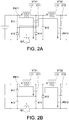
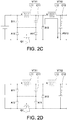
- FIGS. 2A to 2D schematic diagrams of a two-stage power converting procedure of the power converter system 100 of FIG. 1 are shown.
- the charging control diodes A11 and A12 are electrically connected to two ends of the common switch Q1 respectively.
- the common switch Q1 When the common switch Q1 is conducted, the charging control diodes A11 and A12 are automatically connected but the converting control diodes B11 and B12 are automatically disconnected to form a first charging loop PA11 and a second charging loop PA12.
- the first charging loop PA11 is configured to charge the first inductor L11 to store power.
- the second charging loop PA12 is configured to charge the second inductor L12 to store power.
- the converting control diodes B11 and B12 are electrically connected to an input end of the first inductor L11 and an input end of the second inductor L12 respectively.
- the converting control diodes B11 and B12 are automatically connected but the charging control diodes A11 and A12 are automatically disconnected to form a first converting loop PB11 and a second converting loop PB12.
- the first converting loop PB11 enables the first inductor L11 to charge the first capacitor C11.
- the second converting loop PB12 enables the second inductor L12 to charge the second capacitor C12.
- the converting control diode B11 is automatically disconnected, and only the second converting loop PB12 continues to enable the second inductor L12 to charge the second capacitor C12.
- the converting control diode B12 is automatically disconnected to complete the two-stage power converting procedure.
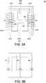
- the coupled two-stage inductor LB can be used to filter the waves in the two loops and suitable allocate the power storage for two times of voltage drop/voltage rise.
- the coupled two-stage inductor LB includes a first structure ST1, a second structure ST2, a first coil CO1 and a second coil CO2.
- the first structure ST1 includes a first cylinder CY1, a second cylinder CY2, and a third cylinder CY3 interposed between the first cylinder CY1 and the second cylinder CY2.
- the first cylinder CY1, the second cylinder CY2 and the third cylinder CY3 are connected by one end, such that the first structure ST1 has an E-shaped appearance.
- the second structure ST2 includes a fourth cylinder CY4, a fifth cylinder CY5, and a sixth cylinder CY6 interposed between the fourth cylinder CY4 and the fifth cylinder CY5.
- the fourth cylinder CY4, the fifth cylinder CY5 and the sixth cylinder CY6 are connected by one end, such that the second structure ST2 has an E-shaped appearance.
- the first structure ST1 and the second structure ST2 are disposed oppositely, such that the first cylinder CY1 corresponds to the fourth cylinder CY4, the second cylinder CY2 corresponds to the fifth cylinder CY5, and the third cylinder CY3 corresponds to the sixth cylinder CY6.
- the first cylinder CY1 and the fourth cylinder CY4 are separated by a first gap G1.
- the second cylinder CY2 and the fifth cylinder CY5 are separated by a second gap G2.
- the third cylinder CY3 and the sixth cylinder CY6 are separated by a third gap G3.
- the first coil CO1 is winded on the first cylinder CY1 and the fourth cylinder CY4.
- the second coil CO2 is winded on the second cylinder CY2 and the fifth cylinder CY5.
- the third cylinder CY3 and the sixth cylinder CY6 are not winded by any coil.
- all of the first cylinder CY1, the second cylinder CY2, the third cylinder CY3, the fourth cylinder CY4, the fifth cylinder CY5 and the sixth cylinder CY6 are magnetic cylinders.
- the first gap G1, the second gap G2 and the third gap G3 can be adjusted according to power distribution, therefore the dimensions of the first gap G1, the second gap G2 and the third gap G3 can be different.
- the number of windings N1 of the first coil CO1 and the number of windings N2 of the second coil CO2 can also be adjusted according to power distribution, and therefore can be different.
- FIG. 3B an equivalent circuit diagram of the coupled two-stage inductor LB of FIG. 3A is shown.
- the first gap G1, the second gap G2 and the third gap G3 respectively form a first magneto-resistance R1, a second magneto-resistance R2 and a third magneto-resistance R3.
- the coupled two-stage inductor LB can obtain the inductance of the first inductor L11 and the inductance of the second inductor L12 using the following equations (1) and (2).
- first magnetic flux ⁇ 1, the second magnetic flux ⁇ 2, the third magnetic flux ⁇ 3 can be correspondingly adjusted through the adjustment of the first gap G1, the second gap G2 and the third gap G3.
- suitable first inductor L11 and second inductor L12 can be designed according to the number of windings N1 and the number of windings N2.
- FIG. 4 a schematic diagram of the coupled two-stage inductor of FIG. 3A used in the power converter system of FIG. 1 is shown.
- the first inductor L11 and the second inductor L12 can be integrated as a coupled two-stage inductor LB.
- one coupled two-stage inductor LB corresponding to the first inductor L11 and the second inductor L12 can be designed. Since the coupled two-stage inductor LB provides the function of two inductors (that is, the first inductor L11 and the second inductor L12), the design of the two-stage power converter system can be simplified.
- the first charging loop PA11 and the second charging loop PA12 can be controlled by the same common switch Q1.
- the power converter system 100 of the present embodiment can increase the step-down ratio by more than 4 times, and therefore can be used in the vehicle power of the power converter system which requires a high step-down ratio.
- the efficiency of the power converter system 100 of the present embodiment is increased by more than 10%, and the cost and the volume are reduced by more than 30% and more than 40%, respectively.
- FIG. 5 a schematic diagram of a power converter system 500 according to another embodiment is shown is shown.
- the power converter system 500 is a buck-boost power converter system.
- the power converter system 500 of FIG. 5 includes a first power converting unit VT51, a second power converting unit VT52, a common switch Q5, two charging control diodes A51 and A52 and two converting control diodes B51 and B52.
- the first power converting unit VT51 is a buck unit.
- the first power converting unit VT51 includes a first inductor L51 and a first capacitor C51.
- the first inductor L51 is electrically connected to the first capacitor C51, and, after storing power, the first inductor L51 is able to charge the first capacitor C51.
- the second power converting unit VT52 is a boost unit.
- the second power converting unit VT52 includes a second inductor L52 and a second capacitor C52.
- the second inductor L52 is electrically connected to the second capacitor C52, and, after storing power, the second inductor L52 is able to charge the second capacitor C52.
- the common switch Q5 is electrically connected to the first power converting unit VT51 and the second power converting unit VT52.
- the first power converting unit VT51 and the second power converting unit VT52 are both operated with the common switch Q5.
- the common switch Q5 When the common switch Q5 is conducted, the first power converting unit VT51 and the second power converting unit VT52 perform a two-stage power converting procedure with in-phase and same time sequence.
- FIGS. 6A to 6D schematic diagrams of a two-stage power converting procedure of the power converter system 500 of FIG. 5 are shown.
- the charging control diodes A51 and A52 are electrically connected to two ends of the common switch Q5 respectively.
- the charging control diodes A51 and A52 are automatically connected but the converting control diodes B51 and B52 are automatically disconnected to form a first charging loop PA51 and a second charging loop PA52.
- the first charging loop PA51 is configured to charge the first inductor L51 to store power.
- the second charging loop PA52 is configured to charge the second inductor L52 to store power.
- the converting control diodes B51 and B52 are electrically connected to an input end of the first inductor L51 and an output end of the second inductor L52 respectively.
- the common switch Q5 When the common switch Q5 is not conducted, the converting control diodes B51 and B52 are automatically connected but the charging control diodes A51 and A52 are automatically disconnected to form a first converting loop PB51 and a second converting loop PB52.
- the first converting loop PB51 enables the first inductor L51 to charge the first capacitor C51.
- the second converting loop PB52 enables the second inductor L52 to charge the second capacitor C52.
- the converting control diode B51 is automatically disconnected, and only the second converting loop PB52 continues to enable the second inductor L52 to charge the second capacitor C52.
- the converting control diode B52 is automatically disconnected to complete the two-stage power converting procedure.
- the coupled two-stage inductor LB of FIG. 3A and FIG. 3B can also be used in the buck-boost power converter system 500 of FIG. 5 .
- the design parameters of the first inductor L51 and the second inductor L52 are similar to that of the above design and the similarities are not repeated here.
- the power converter system 700 is a boost-boost power converter system.
- the power converter system 700 of FIG. 7 includes a first power converting unit VT71, a second power converting unit VT72, a common switch Q7, a charging control diode A71 and two converting control diodes B71 and B72.
- the first power converting unit VT71 is a boost unit.
- the first power converting unit VT71 includes a first inductor L71 and a first capacitor C71.
- the first inductor L71 is electrically connected to the first capacitor C71, and, after storing power, the first inductor L71 is able to charge the first capacitor C71.
- the second power converting unit VT72 is a boost unit.
- the second power converting unit VT72 includes a second inductor L72 and a second capacitor C72.
- the second inductor L72 is electrically connected to the second capacitor C72, and, after storing power, the second inductor L72 is able to charge the second capacitor C72.
- the common switch Q7 is electrically connected to the first power converting unit VT71 and the second power converting unit VT72.
- the first power converting unit VT71 and the second power converting unit VT72 are both operated with the common switch Q7.
- the common switch Q7 When the common switch Q7 is conducted, the first power converting unit VT71 and the second power converting unit VT72 perform a two-stage power converting procedure with in-phase and same time sequence.
- FIGS. 8A to 8D schematic diagrams of a two-stage power converting procedure of the power converter system 700 of FIG. 7 are shown.
- the charging control diode A71 is electrically connected to one end of the common switch Q7.
- the common switch Q7 When the common switch Q7 is conducted, the charging control diode A71 are automatically connected but the converting control diodes B71 and B72 are automatically disconnected to form a first charging loop PA71 and a second charging loop PA72.
- the first charging loop PA71 is configured to charge the first inductor L71 to store power.
- the second charging loop PA72 is configured to charge the second inductor L72 to store power.
- the converting control diodes B71 and B72 are electrically connected to an output end of the first inductor L71 and an output end of the second inductor L72 respectively.
- the common switch Q7 When the common switch Q7 is not conducted, the converting control diodes B71 and B72 are automatically connected but the charging control diode A71 are automatically disconnected to form a first converting loop PB71 and a second converting loop PB72.
- the first converting loop PB71 enables the first inductor L71 to charge the first capacitor C71.
- the second converting loop PB72 enables the second inductor L72 to charge the second capacitor C72.
- the converting control diode B71 is automatically disconnected, and only the second converting loop PB72 continues to enable the second inductor L72 to charge the second capacitor C72.
- the coupled two-stage inductor LB of FIG. 3A and FIG. 3B can also be used in the boost-boost power converter system 700 of FIG. 7 .
- the design parameters of the first inductor L51 and the second inductor L52 are similar to that of the above design and the similarities are not repeated here.
- FIG. 9 a schematic diagram of a power converter system 900 according to another embodiment is shown.
- the power converter system 900 is a boost-buck power converter system.
- the power converter system 900 of FIG. 9 includes a first power converting unit VT91, a second power converting unit VT92, a common switch Q9, a charging control diode A91 and two converting control diodes B91 and B92.
- the first power converting unit VT91 is a boost unit.
- the first power converting unit VT91 includes a first inductor L91 and a first capacitor C91.
- the first inductor L91 is electrically connected to the first capacitor C91, and, after storing power, the first inductor L91 is able to charge the first capacitor C91.
- the second power converting unit VT92 is a buck unit.
- the second power converting unit VT92 includes a second inductor L92 and a second capacitor C92.
- the second inductor L92 is electrically connected to the second capacitor C92, and, after storing power, the second inductor L92 is able to charge the second capacitor C92.
- the common switch Q9 is electrically connected to the first power converting unit VT91 and the second power converting unit VT92.
- the first power converting unit VT91 and the second power converting unit VT92 are both operated with the common switch Q9.
- the common switch Q9 When the common switch Q9 is conducted, the first power converting unit VT91 and the second power converting unit VT92 perform a two-stage power converting procedure with in-phase and same time sequence.
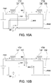
- FIGS. 10A to 10D schematic diagrams of a two-stage power converting procedure of the power converter system 900 of FIG. 9 are shown.
- the charging control diode A91 is electrically connected to one end of the common switch Q9.
- the common switch Q9 When the common switch Q9 is conducted, the charging control diode A91 are automatically connected but the converting control diodes B91 and B92 are automatically disconnected to form a first charging loop PA91 and a second charging loop PA92.
- the first charging loop PA91 is configured to charge the first inductor L91 to store power
- the second charging loop PA92 is configured to charge the second inductor L92 to store power.
- the converting control diodes B91 and B92 are electrically connected to an output end of the first inductor L91 and an input end of the second inductor L92 respectively.
- the common switch Q9 When the common switch Q9 is not conducted, the converting control diodes B91 and B92 are automatically connected but the charging control diode A91 are automatically disconnected to form a first converting loop PB91 and a second converting loop PB92.
- the first converting loop PB91 enables the first inductor L91 to charge the first capacitor C91.
- the second converting loop PB92 enables the second inductor L92 to charge the second capacitor C92.
- the converting control diode B91 is automatically disconnected, and only the second converting loop PB92 continues to enable the second inductor L92 to charge the second capacitor C92.
- the coupled two-stage inductor LB of FIG. 3A and FIG. 3B can also be used in the boost-buck power converter system 900 of FIG. 9 .
- the design parameters of the first inductor L91 and the second inductor L92 are similar to that of the above design and are not repeated here.
- the source of the common switches Q1, Q5, Q7 and Q9 shares the ground with the input voltage, such that the drive signal does not need to be isolated and the circuit cost can be reduced.
- the power converter systems 100, 500, 700 and 900 further use the charging control diodes A11 and A12, A51, A52, A71 and A91 to form the first charging loops PA11, PA51, PA71 and PA91 and the second charging loop PA12, PA52, PA72 and PA92.
- the power converter systems 100, 500, 700 and 900 further use the converting control diodes B11 and B12, B51, B52, B71, B72, B91 and B92 to form the first converting loops PB11, PB51, PB71 and PB91 and the second converting loop PB12, PB52, PB72 and PB92.
- the first power converting units VT11, VT51, VT71 and VT91 and the second power converting units VT12, VT52, VT72 and VT92 can concurrently perform a charging/discharging procedure with in-phase and same time sequence.
- FIG. 11A a current chart of the power converter system 100 of FIG. 1 is shown.
- the first power converting unit VT11 and the second power converting unit VT12 are both operated with the same common switch Q1, and therefore have only one time sequence.
- the first power converting unit VT11 and the second power converting unit VT12 are both operated with the same common switch Q1, therefore the first inductor L11 and the second inductor L12 can be charged at the same time.
- the common switch Q1 is conducted, the current curve IQ1(1) of the common switch Q1 shows that there are electric currents passing through the common switch Q1.
- a comparison of current curves IL11 and IL12 shows that the two inductors have the same current, such that the first power converting unit VT11 and the second power converting unit VT12 can perform a charging/discharging procedure with in-phase and same time sequence.
- FIG. 11B a current chart of the power converter system 500 of FIG. 5 is shown.
- the first power converting unit VT51 and the second power converting unit VT52 are both operated with the same common switch Q1, and therefore have only one time sequence.
- the first power converting unit VT51 and the second power converting unit VT52 are both operated with the same common switch Q1, therefore the first inductor L51 and the second inductor L52 can be charged at the same time.
- the current curve IQ1(5) of the common switch Q1 shows that there are electric currents passing through the current curve IQ1(5).
- a comparison of the current curves IL51 and IL52 shows that the two inductors have the same current, such that the first power converting unit VT51 and the second power converting unit VT522 can perform a charging/discharging procedure with in-phase and same time sequence.
- the current charts of the power converter systems 700 and 900 are similar to the current chart of the power converter system 500.
- the power converter systems 700 and 900 both have the feature of in-phase and same time sequence, and the similarities are not repeated here.
Landscapes
- Engineering & Computer Science (AREA)
- Power Engineering (AREA)
- Dc-Dc Converters (AREA)
Abstract
Description
- The disclosure relates in general to a power converter system and a coupled two-stage inductor.
- Along with the advance in the technology of electronics, various electronic devices are continuously provided one after another. Since different electronic devices may have different voltage specifications, the power converter system is provided. However, the single-stage power converter system with a high step-down ratio makes the duty ratio of switch decrease. The power converter system has poor performance in terms of accuracy and stability, and is susceptible to noise interference, which decreases power conversion efficiency. Furthermore, the control unit used in the power converter system is more expensive.
- The disclosure relates to a power converter system and a coupled two-stage inductor. Through circuit optimization integration, one common switch enables two power converting units to perform a charging/discharging procedure with in-phase and same time sequence, not only greatly increasing the step-down ratio and conversion efficiency but also reducing the cost and the volume.
- According to one embodiment of the disclosure, a power converter system including a first power converting unit, a second power converting unit and a common switch is provided. The first power converting unit includes a first inductor and a first capacitor. The first inductor is electrically connected to the first capacitor. The second power converting unit includes a second inductor and a second capacitor. The second inductor is electrically connected to the second capacitor. The common switch is electrically connected to the first power converting unit and the second power converting unit. The first power converting unit and the second power converting unit are both operated with the common switch. When the common switch is conducted, the first power converting unit and the second power converting unit perform a two-stage power converting procedure with in-phase and same time sequence.
- According to another embodiment of the disclosure, a coupled two-stage inductor including a first structure, a second structure, a first coil and a second coil is provided. The first structure includes a first cylinder, a second cylinder, and a third cylinder interposed between the first cylinder and the second cylinder. The second structure includes a fourth cylinder, a fifth cylinder, and a sixth cylinder interposed between the fourth cylinder and the fifth cylinder. The first structure and the second structure are disposed oppositely, such that the first cylinder and the fourth cylinder are separated by a first gap, the second cylinder and the fifth cylinder are separated by a second gap, and the third cylinder and the sixth cylinder are separated by a third gap. The first coil is winded on the first cylinder and the fourth cylinder. The second coil is winded on the second cylinder and the fifth cylinder.
- According to an embodiment of the disclosure, a power converter system including a first power converting unit, a second power converting unit and a common switch is provided. The first power converting unit includes a first inductor and a first capacitor. The first inductor is electrically connected to the first capacitor. The second power converting unit includes a second inductor and a second capacitor. The second inductor is electrically connected to the second capacitor. The common switch is electrically connected to the first power converting unit and the second power converting unit. The first power converting unit and the second power converting unit are both operated with the common switch. When the common switch is conducted, the first power converting unit and the second power converting unit perform a two-stage power converting procedure with in-phase and same time sequence. The first inductor and the second inductor are integrated as a coupled two-stage inductor.
- The above and other aspects of the disclosure will become better understood with regard to the following detailed description of the preferred but non-limiting embodiment(s). The following description is made with reference to the accompanying drawings.
-
-
FIG. 1 is a schematic diagram of a power converter system according to an embodiment. -
FIGS. 2A to 2D are schematic diagrams of a two-stage power converting procedure of the power converter system ofFIG. 1 . -
FIG. 3A is a schematic diagram of a coupled two-stage inductor according to an embodiment. -
FIG. 3B is an equivalent circuit diagram of the coupled two-stage inductor ofFIG. 3A . -
FIG. 4 is a schematic diagram of the coupled two-stage inductor ofFIG. 3A used in the power converter system ofFIG. 1 . -
FIG. 5 is a schematic diagram of a power converter system according to another embodiment. -
FIGS. 6A to 6D are schematic diagrams of a two-stage power converting procedure of the power converter system ofFIG. 5 . -
FIG. 7 is a schematic diagram of a power converter system according to another embodiment. -
FIGS. 8A to 8D are schematic diagrams of a two-stage power converting procedure of the power converter system ofFIG. 7 . -
FIG. 9 is a schematic diagram of a power converter system according to another embodiment. -
FIGS. 10A to 10D are schematic diagrams of a two-stage power converting procedure of the power converter system ofFIG. 9 . -
FIG. 11A is a current chart of the power converter system ofFIG. 1 . -
FIG. 11B is a current chart of the power converter system ofFIG. 5 . - In the following detailed description, for purposes of explanation, numerous specific details are set forth in order to provide a thorough understanding of the disclosed embodiments. It will be apparent, however, that one or more embodiments may be practiced without these specific details. In other instances, well-known structures and devices are schematically shown in order to simplify the drawing.
- Referring to
FIG. 1 , a schematic diagram of apower converter system 100 according to an embodiment is shown. In an embodiment as indicated inFIG. 1 , thepower converter system 100 is a buck-buck power converter system. Thepower converter system 100 ofFIG. 1 includes a first power converting unit VT11, a second power converting unit VT12, a common switch Q1, two charging control diodes A11 and A12 and two converting control diodes B11 and B12. The first power converting unit VT11 is a buck unit. The first power converting unit VT11 includes a first inductor L11 and a first capacitor C11. The first inductor L11 is electrically connected to the first capacitor C11, and, after storing power, the first inductor L11 is able to charge the first capacitor C11. The second power converting unit VT12 is a buck unit. The second power converting unit VT12 includes a second inductor L12 and a second capacitor C12. The second inductor L12 is electrically connected to the second capacitor C12, and, after storing power, the second inductor L12 is able to charge the second capacitor C12. - The common switch Q1 is electrically connected to the first power converting unit VT11 and the second power converting unit VT12. The first power converting unit VT11 and the second power converting unit VT12 are both operated with the common switch Q1. When the common switch Q1 is conducted, the first power converting unit VT11 and the second power converting unit VT12 perform a two-stage power converting procedure with in-phase and same time sequence.
- Referring to
FIGS. 2A to 2D , schematic diagrams of a two-stage power converting procedure of thepower converter system 100 ofFIG. 1 are shown. As indicated inFIG. 2A , the charging control diodes A11 and A12 are electrically connected to two ends of the common switch Q1 respectively. When the common switch Q1 is conducted, the charging control diodes A11 and A12 are automatically connected but the converting control diodes B11 and B12 are automatically disconnected to form a first charging loop PA11 and a second charging loop PA12. The first charging loop PA11 is configured to charge the first inductor L11 to store power. The second charging loop PA12 is configured to charge the second inductor L12 to store power. - As indicated in
FIG. 2B , the converting control diodes B11 and B12 are electrically connected to an input end of the first inductor L11 and an input end of the second inductor L12 respectively. When the common switch Q1 is not conducted, the converting control diodes B11 and B12 are automatically connected but the charging control diodes A11 and A12 are automatically disconnected to form a first converting loop PB11 and a second converting loop PB12. The first converting loop PB11 enables the first inductor L11 to charge the first capacitor C11. The second converting loop PB12 enables the second inductor L12 to charge the second capacitor C12. - As indicated in
FIG. 2C , when the first inductor L11 completes the procedure for charging the first capacitor C11, the converting control diode B11 is automatically disconnected, and only the second converting loop PB12 continues to enable the second inductor L12 to charge the second capacitor C12. - As indicated in
FIG. 2D , when the second inductor L12 completes the procedure for charging the second capacitor C12, the converting control diode B12 is automatically disconnected to complete the two-stage power converting procedure. - Referring to
FIG. 3A , a schematic diagram of a coupled two-stage inductor LB according to an embodiment is shown. In the above embodiments, the coupled two-stage inductor LB can be used to filter the waves in the two loops and suitable allocate the power storage for two times of voltage drop/voltage rise. The coupled two-stage inductor LB includes a first structure ST1, a second structure ST2, a first coil CO1 and a second coil CO2. The first structure ST1 includes a first cylinder CY1, a second cylinder CY2, and a third cylinder CY3 interposed between the first cylinder CY1 and the second cylinder CY2. The first cylinder CY1, the second cylinder CY2 and the third cylinder CY3 are connected by one end, such that the first structure ST1 has an E-shaped appearance. The second structure ST2 includes a fourth cylinder CY4, a fifth cylinder CY5, and a sixth cylinder CY6 interposed between the fourth cylinder CY4 and the fifth cylinder CY5. The fourth cylinder CY4, the fifth cylinder CY5 and the sixth cylinder CY6 are connected by one end, such that the second structure ST2 has an E-shaped appearance. The first structure ST1 and the second structure ST2 are disposed oppositely, such that the first cylinder CY1 corresponds to the fourth cylinder CY4, the second cylinder CY2 corresponds to the fifth cylinder CY5, and the third cylinder CY3 corresponds to the sixth cylinder CY6. The first cylinder CY1 and the fourth cylinder CY4 are separated by a first gap G1. The second cylinder CY2 and the fifth cylinder CY5 are separated by a second gap G2. The third cylinder CY3 and the sixth cylinder CY6 are separated by a third gap G3. The first coil CO1 is winded on the first cylinder CY1 and the fourth cylinder CY4. The second coil CO2 is winded on the second cylinder CY2 and the fifth cylinder CY5. The third cylinder CY3 and the sixth cylinder CY6 are not winded by any coil. - In the present embodiment, all of the first cylinder CY1, the second cylinder CY2, the third cylinder CY3, the fourth cylinder CY4, the fifth cylinder CY5 and the sixth cylinder CY6 are magnetic cylinders. The first gap G1, the second gap G2 and the third gap G3 can be adjusted according to power distribution, therefore the dimensions of the first gap G1, the second gap G2 and the third gap G3 can be different. Besides, the number of windings N1 of the first coil CO1 and the number of windings N2 of the second coil CO2 can also be adjusted according to power distribution, and therefore can be different.
- Referring to
FIG. 3B , an equivalent circuit diagram of the coupled two-stage inductor LB ofFIG. 3A is shown. The first gap G1, the second gap G2 and the third gap G3 respectively form a first magneto-resistance R1, a second magneto-resistance R2 and a third magneto-resistance R3. The coupled two-stage inductor LB can obtain the inductance of the first inductor L11 and the inductance of the second inductor L12 using the following equations (1) and (2).

- That is, the first magnetic flux Ø1, the second magnetic flux Ø2, the third magnetic flux Ø3 can be correspondingly adjusted through the adjustment of the first gap G1, the second gap G2 and the third gap G3. Then, suitable first inductor L11 and second inductor L12 can be designed according to the number of windings N1 and the number of windings N2.
- Referring to
FIG. 4 , a schematic diagram of the coupled two-stage inductor ofFIG. 3A used in the power converter system ofFIG. 1 is shown. The first inductor L11 and the second inductor L12 can be integrated as a coupled two-stage inductor LB. Based on the requirement of the power converter system, one coupled two-stage inductor LB corresponding to the first inductor L11 and the second inductor L12 can be designed. Since the coupled two-stage inductor LB provides the function of two inductors (that is, the first inductor L11 and the second inductor L12), the design of the two-stage power converter system can be simplified. - According to the design of the above embodiments, the first charging loop PA11 and the second charging loop PA12 can be controlled by the same common switch Q1. In comparison to the single-stage power converter system, the
power converter system 100 of the present embodiment can increase the step-down ratio by more than 4 times, and therefore can be used in the vehicle power of the power converter system which requires a high step-down ratio. In comparison to the existing dual-stage power converter system, the efficiency of thepower converter system 100 of the present embodiment is increased by more than 10%, and the cost and the volume are reduced by more than 30% and more than 40%, respectively. - The design of the above embodiments can also be used in other embodiments. Referring to
FIG. 5 , a schematic diagram of apower converter system 500 according to another embodiment is shown is shown. In an embodiment as indicated inFIG. 5 , thepower converter system 500 is a buck-boost power converter system. Thepower converter system 500 ofFIG. 5 includes a first power converting unit VT51, a second power converting unit VT52, a common switch Q5, two charging control diodes A51 and A52 and two converting control diodes B51 and B52. The first power converting unit VT51 is a buck unit. The first power converting unit VT51 includes a first inductor L51 and a first capacitor C51. The first inductor L51 is electrically connected to the first capacitor C51, and, after storing power, the first inductor L51 is able to charge the first capacitor C51. The second power converting unit VT52 is a boost unit. The second power converting unit VT52 includes a second inductor L52 and a second capacitor C52. The second inductor L52 is electrically connected to the second capacitor C52, and, after storing power, the second inductor L52 is able to charge the second capacitor C52. - The common switch Q5 is electrically connected to the first power converting unit VT51 and the second power converting unit VT52. The first power converting unit VT51 and the second power converting unit VT52 are both operated with the common switch Q5. When the common switch Q5 is conducted, the first power converting unit VT51 and the second power converting unit VT52 perform a two-stage power converting procedure with in-phase and same time sequence.
- Referring to
FIGS. 6A to 6D , schematic diagrams of a two-stage power converting procedure of thepower converter system 500 ofFIG. 5 are shown. As indicated inFIG. 6A , the charging control diodes A51 and A52 are electrically connected to two ends of the common switch Q5 respectively. When the common switch Q5 is conducted, the charging control diodes A51 and A52 are automatically connected but the converting control diodes B51 and B52 are automatically disconnected to form a first charging loop PA51 and a second charging loop PA52. The first charging loop PA51 is configured to charge the first inductor L51 to store power. The second charging loop PA52 is configured to charge the second inductor L52 to store power. - As indicated in
FIG. 6B , the converting control diodes B51 and B52 are electrically connected to an input end of the first inductor L51 and an output end of the second inductor L52 respectively. When the common switch Q5 is not conducted, the converting control diodes B51 and B52 are automatically connected but the charging control diodes A51 and A52 are automatically disconnected to form a first converting loop PB51 and a second converting loop PB52. The first converting loop PB51 enables the first inductor L51 to charge the first capacitor C51. The second converting loop PB52 enables the second inductor L52 to charge the second capacitor C52. - As indicated in
FIG. 6C , when the first inductor L51 completes the procedure for charging the first capacitor C51, the converting control diode B51 is automatically disconnected, and only the second converting loop PB52 continues to enable the second inductor L52 to charge the second capacitor C52. - As indicated in
FIG. 6D , when the second inductor L52 completes the procedure for charging the second capacitor C52, the converting control diode B52 is automatically disconnected to complete the two-stage power converting procedure. - It should be noted that the coupled two-stage inductor LB of
FIG. 3A and FIG. 3B can also be used in the buck-boostpower converter system 500 ofFIG. 5 . The design parameters of the first inductor L51 and the second inductor L52 are similar to that of the above design and the similarities are not repeated here. - Referring to
FIG. 7 , a schematic diagram of apower converter system 700 according to another embodiment is shown. In an embodiment as indicated inFIG. 7 , thepower converter system 700 is a boost-boost power converter system. Thepower converter system 700 ofFIG. 7 includes a first power converting unit VT71, a second power converting unit VT72, a common switch Q7, a charging control diode A71 and two converting control diodes B71 and B72. The first power converting unit VT71 is a boost unit. The first power converting unit VT71 includes a first inductor L71 and a first capacitor C71. The first inductor L71 is electrically connected to the first capacitor C71, and, after storing power, the first inductor L71 is able to charge the first capacitor C71. The second power converting unit VT72 is a boost unit. The second power converting unit VT72 includes a second inductor L72 and a second capacitor C72. The second inductor L72 is electrically connected to the second capacitor C72, and, after storing power, the second inductor L72 is able to charge the second capacitor C72. - The common switch Q7 is electrically connected to the first power converting unit VT71 and the second power converting unit VT72. The first power converting unit VT71 and the second power converting unit VT72 are both operated with the common switch Q7. When the common switch Q7 is conducted, the first power converting unit VT71 and the second power converting unit VT72 perform a two-stage power converting procedure with in-phase and same time sequence.
- Referring to
FIGS. 8A to 8D , schematic diagrams of a two-stage power converting procedure of thepower converter system 700 ofFIG. 7 are shown. As indicated inFIG. 8A , the charging control diode A71 is electrically connected to one end of the common switch Q7. When the common switch Q7 is conducted, the charging control diode A71 are automatically connected but the converting control diodes B71 and B72 are automatically disconnected to form a first charging loop PA71 and a second charging loop PA72. The first charging loop PA71 is configured to charge the first inductor L71 to store power. The second charging loop PA72 is configured to charge the second inductor L72 to store power. - As indicated in
FIG. 8B , the converting control diodes B71 and B72 are electrically connected to an output end of the first inductor L71 and an output end of the second inductor L72 respectively. When the common switch Q7 is not conducted, the converting control diodes B71 and B72 are automatically connected but the charging control diode A71 are automatically disconnected to form a first converting loop PB71 and a second converting loop PB72. The first converting loop PB71 enables the first inductor L71 to charge the first capacitor C71. The second converting loop PB72 enables the second inductor L72 to charge the second capacitor C72. - As indicated in
FIG. 8C , when the first inductor L71 completes the procedure for charging the first capacitor C71, the converting control diode B71 is automatically disconnected, and only the second converting loop PB72 continues to enable the second inductor L72 to charge the second capacitor C72. - As indicated in
FIG. 8D , when the second inductor L72 completes the procedure for charging the second capacitor C72, the converting control diode B72 is automatically disconnected to complete the two-stage power converting procedure. - It should be noted that the coupled two-stage inductor LB of
FIG. 3A and FIG. 3B can also be used in the boost-boostpower converter system 700 ofFIG. 7 . The design parameters of the first inductor L71 and the second inductor L72. The design parameters of the first inductor L51 and the second inductor L52 are similar to that of the above design and the similarities are not repeated here. - Referring to
FIG. 9 , a schematic diagram of apower converter system 900 according to another embodiment is shown. In an embodiment as indicated inFIG. 9 , thepower converter system 900 is a boost-buck power converter system. Thepower converter system 900 ofFIG. 9 includes a first power converting unit VT91, a second power converting unit VT92, a common switch Q9, a charging control diode A91 and two converting control diodes B91 and B92. The first power converting unit VT91 is a boost unit. The first power converting unit VT91 includes a first inductor L91 and a first capacitor C91. The first inductor L91 is electrically connected to the first capacitor C91, and, after storing power, the first inductor L91 is able to charge the first capacitor C91. The second power converting unit VT92 is a buck unit. The second power converting unit VT92 includes a second inductor L92 and a second capacitor C92. The second inductor L92 is electrically connected to the second capacitor C92, and, after storing power, the second inductor L92 is able to charge the second capacitor C92. - The common switch Q9 is electrically connected to the first power converting unit VT91 and the second power converting unit VT92. The first power converting unit VT91 and the second power converting unit VT92 are both operated with the common switch Q9. When the common switch Q9 is conducted, the first power converting unit VT91 and the second power converting unit VT92 perform a two-stage power converting procedure with in-phase and same time sequence.
- Referring to
FIGS. 10A to 10D , schematic diagrams of a two-stage power converting procedure of thepower converter system 900 ofFIG. 9 are shown. As indicated inFIG. 10A , the charging control diode A91 is electrically connected to one end of the common switch Q9. When the common switch Q9 is conducted, the charging control diode A91 are automatically connected but the converting control diodes B91 and B92 are automatically disconnected to form a first charging loop PA91 and a second charging loop PA92. The first charging loop PA91 is configured to charge the first inductor L91 to store power, the second charging loop PA92 is configured to charge the second inductor L92 to store power. - As indicated in
FIG. 10B , the converting control diodes B91 and B92 are electrically connected to an output end of the first inductor L91 and an input end of the second inductor L92 respectively. When the common switch Q9 is not conducted, the converting control diodes B91 and B92 are automatically connected but the charging control diode A91 are automatically disconnected to form a first converting loop PB91 and a second converting loop PB92. The first converting loop PB91 enables the first inductor L91 to charge the first capacitor C91. The second converting loop PB92 enables the second inductor L92 to charge the second capacitor C92. - As indicated in
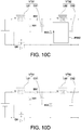
FIG. 10C , when the first inductor L91 completes the procedure for charging the first capacitor C91, the converting control diode B91 is automatically disconnected, and only the second converting loop PB92 continues to enable the second inductor L92 to charge the second capacitor C92. - As indicated in
FIG. 10D , when the second inductor L92 completes the procedure for charging the second capacitor C92, the converting control diode B92 is automatically disconnected to complete the two-stage power converting procedure. - It should be noted that the coupled two-stage inductor LB of
FIG. 3A and FIG. 3B can also be used in the boost-buckpower converter system 900 ofFIG. 9 . The design parameters of the first inductor L91 and the second inductor L92 are similar to that of the above design and are not repeated here. - In the
power converter systems - Besides, the
power converter systems power converter systems - Referring to
FIG. 11A , a current chart of thepower converter system 100 ofFIG. 1 is shown. In thepower converter system 100, the first power converting unit VT11 and the second power converting unit VT12 are both operated with the same common switch Q1, and therefore have only one time sequence. Also, in thepower converter system 100, the first power converting unit VT11 and the second power converting unit VT12 are both operated with the same common switch Q1, therefore the first inductor L11 and the second inductor L12 can be charged at the same time. When the common switch Q1 is conducted, the current curve IQ1(1) of the common switch Q1 shows that there are electric currents passing through the common switch Q1. A comparison of current curves IL11 and IL12 shows that the two inductors have the same current, such that the first power converting unit VT11 and the second power converting unit VT12 can perform a charging/discharging procedure with in-phase and same time sequence. - Referring to
FIG. 11B , a current chart of thepower converter system 500 ofFIG. 5 is shown. In thepower converter system 500, the first power converting unit VT51 and the second power converting unit VT52 are both operated with the same common switch Q1, and therefore have only one time sequence. Moreover, in thepower converter system 500, the first power converting unit VT51 and the second power converting unit VT52 are both operated with the same common switch Q1, therefore the first inductor L51 and the second inductor L52 can be charged at the same time. When the common switch Q1 is conducted, the current curve IQ1(5) of the common switch Q1 shows that there are electric currents passing through the current curve IQ1(5). A comparison of the current curves IL51 and IL52 shows that the two inductors have the same current, such that the first power converting unit VT51 and the second power converting unit VT522 can perform a charging/discharging procedure with in-phase and same time sequence. - The current charts of the
power converter systems power converter system 500. Thepower converter systems - It will be apparent to those skilled in the art that various modifications and variations can be made to the disclosed embodiments. It is intended that the specification and examples be considered as exemplary only, with a true scope of the disclosure being indicated by the following claims and their equivalents.
Claims (15)
- A power converter system (100), wherein the power converter system comprises:a first power converting unit (VT11), comprising a first inductor (L11) and a first capacitor (C11), wherein the first inductor (L11) is electrically connected to the first capacitor (C11);a second power converting unit (VT12), comprising a second inductor (L12) and a second capacitor (C12), wherein the second inductor (L12) is electrically connected to the second capacitor (C12); anda common switch (Q1) electrically connected to the first power converting unit (VT11) and the second power converting unit (VT12), wherein the first power converting unit (VT11) and the second power converting unit (VT12) are both operated with the common switch (Q1), and when the common switch (Q1) is conducted, the first power converting unit (VT11) and the second power converting unit (VT12) perform a two-stage power converting procedure with in-phase and same time sequence.
- The power converter system according to claim 1, further comprising:at least one charging control diode electrically connected to the common switch, wherein when the common switch is conducted, the at least one charging control diode is connected to form a first charging loop and a second charging loop, the first charging loop charges the first inductor, and the second charging loop charges the second inductor.
- The power converter system according to claim 2, wherein the first power converting unit is a buck unit, the second power converting unit is a buck unit, the quantity of the at least one charging control diode is two, and the two charging control diodes are electrically connected to two ends of the common switch respectively.
- The power converter system according to claim 2, wherein the first power converting unit is a buck unit, the second power converting unit is a boost unit, the quantity of the at least one charging control diode is two, and the two charging control diodes are electrically connected to two ends of the common switch respectively.
- The power converter system according to claim 2, wherein the first power converting unit is a boost unit, the second power converting unit is a boost unit, the quantity of the at least one charging control diode is one, and the charging control diode is electrically connected to one end of the common switch.
- The power converter system according to claim 2, wherein the first power converting unit is a boost unit, the second power converting unit is a buck unit, the quantity of the at least one charging control diode is one, and the charging control diode is electrically connected to one end of the common switch.
- The power converter system according to anyone of the claims 1 to 6, further comprising:at least one converting control diode electrically connected to the first power converting unit or the second power converting unit, wherein when the common switch is not conducted, the at least one converting control diode is connected to form a first converting loop and a second converting loop, the first converting loop enables the first inductor to charge the first capacitor, and the second converting loop enables the second inductor to charge the second capacitor.
- The power converter system according to claim 7, wherein the first power converting unit is a buck unit, the second power converting unit is a buck unit, the quantity of the at least one converting control diode is two, and the two converting control diodes are electrically connected to an input end of the first inductor and an input end of the second inductor respectively.
- The power converter system according to claim 7, wherein the first power converting unit is a buck unit, the second power converting unit is a boost unit, the quantity of the at least one converting control diode is two, and the two converting control diodes are electrically connected to an input end of the first inductor and an output end of the second inductor respectively.
- The power converter system according to claim 7, wherein the first power converting unit is a boost unit, the second power converting unit is a boost unit, the quantity of the at least one converting control diode is two, and the two converting control diodes are electrically connected to an output end of the first inductor and an output end of the second inductor respectively.
- The power converter system according to claim 7, wherein the first power converting unit is a boost unit, the second power converting unit is a buck unit, the quantity of the at least one converting control diode is two, and the two converting control diodes are electrically connected to an output end of the first inductor and an input end of the second inductor respectively.
- The power converter system according to anyone of the claims 1 to 11, wherein the first inductor and the second inductor are integrated as a coupled two-stage inductor, and the coupled two-stage inductor comprises:a first structure, comprising:a first cylinder;a second cylinder; anda third cylinder interposed between the first cylinder and the second cylinder;a second structure, comprising:a fourth cylinder;a fifth cylinder; anda sixth cylinder interposed between the fourth cylinder and the fifth cylinder, wherein the first structure and the second structure are disposed oppositely, such that the first cylinder and the fourth cylinder are separated by a first gap, the second cylinder and the fifth cylinder are separated by a second gap, and the third cylinder and the sixth cylinder are separated by a third gap;a first coil winded on the first cylinder and the fourth cylinder; anda second coil winded on the second cylinder and the fifth cylinder.
- The power converter system according to claim 12, wherein all of the first cylinder, the second cylinder, the third cylinder, the fourth cylinder, the fifth cylinder and the sixth cylinder are magnetic cylinders.
- The power converter system according to claim 12 or 13, wherein the number of windings of the first coil and the number of windings of the second coil can be different.
- The power converter system according to anyone of the claims 12 to 14, wherein the dimensions of the first gap, the second gap and the third gap can be different.
Applications Claiming Priority (1)
| Application Number | Priority Date | Filing Date | Title |
|---|---|---|---|
| TW107138097A TWI696340B (en) | 2018-10-26 | 2018-10-26 | Power converter system and coupled two-stage inductor |
Publications (2)
| Publication Number | Publication Date |
|---|---|
| EP3644487A1 true EP3644487A1 (en) | 2020-04-29 |
| EP3644487B1 EP3644487B1 (en) | 2021-07-07 |
Family
ID=65243382
Family Applications (1)
| Application Number | Title | Priority Date | Filing Date |
|---|---|---|---|
| EP19154150.7A Active EP3644487B1 (en) | 2018-10-26 | 2019-01-29 | Power converter system and coupled two-stage inductor |
Country Status (4)
| Country | Link |
|---|---|
| EP (1) | EP3644487B1 (en) |
| CN (1) | CN111106738B (en) |
| ES (1) | ES2893230T3 (en) |
| TW (1) | TWI696340B (en) |
Citations (4)
| Publication number | Priority date | Publication date | Assignee | Title |
|---|---|---|---|---|
| US4857822A (en) * | 1987-09-23 | 1989-08-15 | Virginia Tech Intellectual Properties, Inc. | Zero-voltage-switched multi-resonant converters including the buck and forward type |
| US6304460B1 (en) * | 2000-05-05 | 2001-10-16 | Slobodan Cuk | Switching DC-to-DC converter utilizing a soft switching technique |
| US8772967B1 (en) * | 2011-03-04 | 2014-07-08 | Volterra Semiconductor Corporation | Multistage and multiple-output DC-DC converters having coupled inductors |
| CN104753335A (en) * | 2014-07-10 | 2015-07-01 | 西南交通大学 | Quadratic form Buck power factor correction converter |
Family Cites Families (5)
| Publication number | Priority date | Publication date | Assignee | Title |
|---|---|---|---|---|
| TWI477044B (en) * | 2012-08-10 | 2015-03-11 | Univ Nat Kaohsiung Marine | Step-down rectifier |
| TWI514730B (en) * | 2014-06-16 | 2015-12-21 | Univ Nat Taipei Technology | Ultra high step-down converter |
| TWM548595U (en) * | 2016-10-07 | 2017-09-11 | 心誠鎂行動醫電股份有限公司 | Circuit for atomizing liquid and device thereof |
| TWI625033B (en) * | 2017-03-31 | 2018-05-21 | 崑山科技大學 | Interleaved direct-current boost device |
| CN107360648A (en) * | 2017-07-28 | 2017-11-17 | 株洲麦格米特电气有限责任公司 | A kind of two paths of LED of Buck topologys flows drive circuit |
-
2018
- 2018-10-26 TW TW107138097A patent/TWI696340B/en active
- 2018-11-12 CN CN201811342664.0A patent/CN111106738B/en active Active
-
2019
- 2019-01-29 ES ES19154150T patent/ES2893230T3/en active Active
- 2019-01-29 EP EP19154150.7A patent/EP3644487B1/en active Active
Patent Citations (4)
| Publication number | Priority date | Publication date | Assignee | Title |
|---|---|---|---|---|
| US4857822A (en) * | 1987-09-23 | 1989-08-15 | Virginia Tech Intellectual Properties, Inc. | Zero-voltage-switched multi-resonant converters including the buck and forward type |
| US6304460B1 (en) * | 2000-05-05 | 2001-10-16 | Slobodan Cuk | Switching DC-to-DC converter utilizing a soft switching technique |
| US8772967B1 (en) * | 2011-03-04 | 2014-07-08 | Volterra Semiconductor Corporation | Multistage and multiple-output DC-DC converters having coupled inductors |
| CN104753335A (en) * | 2014-07-10 | 2015-07-01 | 西南交通大学 | Quadratic form Buck power factor correction converter |
Also Published As
| Publication number | Publication date |
|---|---|
| CN111106738A (en) | 2020-05-05 |
| TW202017301A (en) | 2020-05-01 |
| TWI696340B (en) | 2020-06-11 |
| CN111106738B (en) | 2021-07-09 |
| ES2893230T3 (en) | 2022-02-08 |
| EP3644487B1 (en) | 2021-07-07 |
Similar Documents
| Publication | Publication Date | Title |
|---|---|---|
| US10427532B2 (en) | On-board and wireless vehicle charging systems with shared components | |
| CN110326183B (en) | Charging device and vehicle power supply unit | |
| JP5710731B2 (en) | Battery cell module balancing control circuit using LC series resonance | |
| CN108512423B (en) | A high-efficiency and high-power vehicle-mounted DCDC power supply | |
| US9887553B2 (en) | Electric power transmission device, and electric power reception device and vehicle including the same | |
| CN112311232B (en) | A switched capacitor DC/DC converter, switching power supply and control method | |
| Colak et al. | A constant resistance analysis and control of cascaded buck and boost converter for wireless EV chargers | |
| US9991818B2 (en) | Apparatuses and related methods for a wireless power receiver using coupled inductors | |
| US9230748B1 (en) | Hybrid energy storage module | |
| US11990831B2 (en) | Hybrid buck boost converter with reduced inductor current | |
| JP2017005790A (en) | Wireless power transmission system | |
| JP2014007942A (en) | Bidirectional power transmission apparatus | |
| CN107636930A (en) | Contactless power supply system and current-collecting device | |
| JP5794563B2 (en) | Contactless power supply system | |
| CN112572193A (en) | Vehicle-mounted charging system and vehicle with same | |
| Krestovnikov et al. | Concept of a synchronous rectifier for wireless power transfer system | |
| US20210067047A1 (en) | Vehicle power control systems | |
| Chen et al. | A new bidirectional DC-DC converter with a high step-up/down conversion ratio for renewable energy applications | |
| EP3644487B1 (en) | Power converter system and coupled two-stage inductor | |
| Chen et al. | Two/Three-coil hybrid topology for WPT systems charging electric bicycles | |
| KR20190116004A (en) | Variable capacity power bank system | |
| Sattarov et al. | Research of a multifunctional integrated electromagnetic component as an LC filter in DC/DC converters | |
| US20120056475A1 (en) | Vehicle-Used Power Supply System | |
| Khalilian et al. | A hybrid topology wireless power transfer system with constant current or constant voltage output for battery charging application | |
| US20240030830A1 (en) | Ac/dc converter and control method thereof for charging electrical vehicles |
Legal Events
| Date | Code | Title | Description |
|---|---|---|---|
| PUAI | Public reference made under article 153(3) epc to a published international application that has entered the european phase |
Free format text: ORIGINAL CODE: 0009012 |
|
| STAA | Information on the status of an ep patent application or granted ep patent |
Free format text: STATUS: REQUEST FOR EXAMINATION WAS MADE |
|
| STAA | Information on the status of an ep patent application or granted ep patent |
Free format text: STATUS: EXAMINATION IS IN PROGRESS |
|
| 17P | Request for examination filed |
Effective date: 20190129 |
|
| AK | Designated contracting states |
Kind code of ref document: A1 Designated state(s): AL AT BE BG CH CY CZ DE DK EE ES FI FR GB GR HR HU IE IS IT LI LT LU LV MC MK MT NL NO PL PT RO RS SE SI SK SM TR |
|
| AX | Request for extension of the european patent |
Extension state: BA ME |
|
| 17Q | First examination report despatched |
Effective date: 20200408 |
|
| GRAP | Despatch of communication of intention to grant a patent |
Free format text: ORIGINAL CODE: EPIDOSNIGR1 |
|
| STAA | Information on the status of an ep patent application or granted ep patent |
Free format text: STATUS: GRANT OF PATENT IS INTENDED |
|
| RIC1 | Information provided on ipc code assigned before grant |
Ipc: H02M 3/158 20060101AFI20210318BHEP Ipc: H02M 1/00 20060101ALN20210318BHEP |
|
| INTG | Intention to grant announced |
Effective date: 20210406 |
|
| GRAS | Grant fee paid |
Free format text: ORIGINAL CODE: EPIDOSNIGR3 |
|
| GRAA | (expected) grant |
Free format text: ORIGINAL CODE: 0009210 |
|
| STAA | Information on the status of an ep patent application or granted ep patent |
Free format text: STATUS: THE PATENT HAS BEEN GRANTED |
|
| AK | Designated contracting states |
Kind code of ref document: B1 Designated state(s): AL AT BE BG CH CY CZ DE DK EE ES FI FR GB GR HR HU IE IS IT LI LT LU LV MC MK MT NL NO PL PT RO RS SE SI SK SM TR |
|
| REG | Reference to a national code |
Ref country code: GB Ref legal event code: FG4D |
|
| REG | Reference to a national code |
Ref country code: AT Ref legal event code: REF Ref document number: 1409541 Country of ref document: AT Kind code of ref document: T Effective date: 20210715 |
|
| REG | Reference to a national code |
Ref country code: DE Ref legal event code: R096 Ref document number: 602019005802 Country of ref document: DE |
|
| REG | Reference to a national code |
Ref country code: IE Ref legal event code: FG4D |
|
| REG | Reference to a national code |
Ref country code: LT Ref legal event code: MG9D |
|
| REG | Reference to a national code |
Ref country code: NL Ref legal event code: MP Effective date: 20210707 |
|
| REG | Reference to a national code |
Ref country code: AT Ref legal event code: MK05 Ref document number: 1409541 Country of ref document: AT Kind code of ref document: T Effective date: 20210707 |
|
| PG25 | Lapsed in a contracting state [announced via postgrant information from national office to epo] |
Ref country code: HR Free format text: LAPSE BECAUSE OF FAILURE TO SUBMIT A TRANSLATION OF THE DESCRIPTION OR TO PAY THE FEE WITHIN THE PRESCRIBED TIME-LIMIT Effective date: 20210707 Ref country code: PT Free format text: LAPSE BECAUSE OF FAILURE TO SUBMIT A TRANSLATION OF THE DESCRIPTION OR TO PAY THE FEE WITHIN THE PRESCRIBED TIME-LIMIT Effective date: 20211108 Ref country code: NO Free format text: LAPSE BECAUSE OF FAILURE TO SUBMIT A TRANSLATION OF THE DESCRIPTION OR TO PAY THE FEE WITHIN THE PRESCRIBED TIME-LIMIT Effective date: 20211007 Ref country code: NL Free format text: LAPSE BECAUSE OF FAILURE TO SUBMIT A TRANSLATION OF THE DESCRIPTION OR TO PAY THE FEE WITHIN THE PRESCRIBED TIME-LIMIT Effective date: 20210707 Ref country code: BG Free format text: LAPSE BECAUSE OF FAILURE TO SUBMIT A TRANSLATION OF THE DESCRIPTION OR TO PAY THE FEE WITHIN THE PRESCRIBED TIME-LIMIT Effective date: 20211007 Ref country code: AT Free format text: LAPSE BECAUSE OF FAILURE TO SUBMIT A TRANSLATION OF THE DESCRIPTION OR TO PAY THE FEE WITHIN THE PRESCRIBED TIME-LIMIT Effective date: 20210707 Ref country code: LT Free format text: LAPSE BECAUSE OF FAILURE TO SUBMIT A TRANSLATION OF THE DESCRIPTION OR TO PAY THE FEE WITHIN THE PRESCRIBED TIME-LIMIT Effective date: 20210707 Ref country code: SE Free format text: LAPSE BECAUSE OF FAILURE TO SUBMIT A TRANSLATION OF THE DESCRIPTION OR TO PAY THE FEE WITHIN THE PRESCRIBED TIME-LIMIT Effective date: 20210707 Ref country code: RS Free format text: LAPSE BECAUSE OF FAILURE TO SUBMIT A TRANSLATION OF THE DESCRIPTION OR TO PAY THE FEE WITHIN THE PRESCRIBED TIME-LIMIT Effective date: 20210707 Ref country code: FI Free format text: LAPSE BECAUSE OF FAILURE TO SUBMIT A TRANSLATION OF THE DESCRIPTION OR TO PAY THE FEE WITHIN THE PRESCRIBED TIME-LIMIT Effective date: 20210707 |
|
| REG | Reference to a national code |
Ref country code: ES Ref legal event code: FG2A Ref document number: 2893230 Country of ref document: ES Kind code of ref document: T3 Effective date: 20220208 |
|
| PG25 | Lapsed in a contracting state [announced via postgrant information from national office to epo] |
Ref country code: PL Free format text: LAPSE BECAUSE OF FAILURE TO SUBMIT A TRANSLATION OF THE DESCRIPTION OR TO PAY THE FEE WITHIN THE PRESCRIBED TIME-LIMIT Effective date: 20210707 Ref country code: LV Free format text: LAPSE BECAUSE OF FAILURE TO SUBMIT A TRANSLATION OF THE DESCRIPTION OR TO PAY THE FEE WITHIN THE PRESCRIBED TIME-LIMIT Effective date: 20210707 Ref country code: GR Free format text: LAPSE BECAUSE OF FAILURE TO SUBMIT A TRANSLATION OF THE DESCRIPTION OR TO PAY THE FEE WITHIN THE PRESCRIBED TIME-LIMIT Effective date: 20211008 |
|
| REG | Reference to a national code |
Ref country code: DE Ref legal event code: R097 Ref document number: 602019005802 Country of ref document: DE |
|
| PG25 | Lapsed in a contracting state [announced via postgrant information from national office to epo] |
Ref country code: DK Free format text: LAPSE BECAUSE OF FAILURE TO SUBMIT A TRANSLATION OF THE DESCRIPTION OR TO PAY THE FEE WITHIN THE PRESCRIBED TIME-LIMIT Effective date: 20210707 |
|
| PLBE | No opposition filed within time limit |
Free format text: ORIGINAL CODE: 0009261 |
|
| STAA | Information on the status of an ep patent application or granted ep patent |
Free format text: STATUS: NO OPPOSITION FILED WITHIN TIME LIMIT |
|
| PG25 | Lapsed in a contracting state [announced via postgrant information from national office to epo] |
Ref country code: SM Free format text: LAPSE BECAUSE OF FAILURE TO SUBMIT A TRANSLATION OF THE DESCRIPTION OR TO PAY THE FEE WITHIN THE PRESCRIBED TIME-LIMIT Effective date: 20210707 Ref country code: SK Free format text: LAPSE BECAUSE OF FAILURE TO SUBMIT A TRANSLATION OF THE DESCRIPTION OR TO PAY THE FEE WITHIN THE PRESCRIBED TIME-LIMIT Effective date: 20210707 Ref country code: RO Free format text: LAPSE BECAUSE OF FAILURE TO SUBMIT A TRANSLATION OF THE DESCRIPTION OR TO PAY THE FEE WITHIN THE PRESCRIBED TIME-LIMIT Effective date: 20210707 Ref country code: EE Free format text: LAPSE BECAUSE OF FAILURE TO SUBMIT A TRANSLATION OF THE DESCRIPTION OR TO PAY THE FEE WITHIN THE PRESCRIBED TIME-LIMIT Effective date: 20210707 Ref country code: CZ Free format text: LAPSE BECAUSE OF FAILURE TO SUBMIT A TRANSLATION OF THE DESCRIPTION OR TO PAY THE FEE WITHIN THE PRESCRIBED TIME-LIMIT Effective date: 20210707 Ref country code: AL Free format text: LAPSE BECAUSE OF FAILURE TO SUBMIT A TRANSLATION OF THE DESCRIPTION OR TO PAY THE FEE WITHIN THE PRESCRIBED TIME-LIMIT Effective date: 20210707 |
|
| 26N | No opposition filed |
Effective date: 20220408 |
|
| PG25 | Lapsed in a contracting state [announced via postgrant information from national office to epo] |
Ref country code: IT Free format text: LAPSE BECAUSE OF FAILURE TO SUBMIT A TRANSLATION OF THE DESCRIPTION OR TO PAY THE FEE WITHIN THE PRESCRIBED TIME-LIMIT Effective date: 20210707 |
|
| PG25 | Lapsed in a contracting state [announced via postgrant information from national office to epo] |
Ref country code: MC Free format text: LAPSE BECAUSE OF FAILURE TO SUBMIT A TRANSLATION OF THE DESCRIPTION OR TO PAY THE FEE WITHIN THE PRESCRIBED TIME-LIMIT Effective date: 20210707 |
|
| REG | Reference to a national code |
Ref country code: CH Ref legal event code: PL |
|
| REG | Reference to a national code |
Ref country code: BE Ref legal event code: MM Effective date: 20220131 |
|
| PG25 | Lapsed in a contracting state [announced via postgrant information from national office to epo] |
Ref country code: LU Free format text: LAPSE BECAUSE OF NON-PAYMENT OF DUE FEES Effective date: 20220129 |
|
| PG25 | Lapsed in a contracting state [announced via postgrant information from national office to epo] |
Ref country code: BE Free format text: LAPSE BECAUSE OF NON-PAYMENT OF DUE FEES Effective date: 20220131 |
|
| PG25 | Lapsed in a contracting state [announced via postgrant information from national office to epo] |
Ref country code: LI Free format text: LAPSE BECAUSE OF NON-PAYMENT OF DUE FEES Effective date: 20220131 Ref country code: CH Free format text: LAPSE BECAUSE OF NON-PAYMENT OF DUE FEES Effective date: 20220131 |
|
| PG25 | Lapsed in a contracting state [announced via postgrant information from national office to epo] |
Ref country code: IE Free format text: LAPSE BECAUSE OF NON-PAYMENT OF DUE FEES Effective date: 20220129 |
|
| GBPC | Gb: european patent ceased through non-payment of renewal fee |
Effective date: 20230129 |
|
| PG25 | Lapsed in a contracting state [announced via postgrant information from national office to epo] |
Ref country code: GB Free format text: LAPSE BECAUSE OF NON-PAYMENT OF DUE FEES Effective date: 20230129 |
|
| PG25 | Lapsed in a contracting state [announced via postgrant information from national office to epo] |
Ref country code: MK Free format text: LAPSE BECAUSE OF FAILURE TO SUBMIT A TRANSLATION OF THE DESCRIPTION OR TO PAY THE FEE WITHIN THE PRESCRIBED TIME-LIMIT Effective date: 20210707 Ref country code: CY Free format text: LAPSE BECAUSE OF FAILURE TO SUBMIT A TRANSLATION OF THE DESCRIPTION OR TO PAY THE FEE WITHIN THE PRESCRIBED TIME-LIMIT Effective date: 20210707 |
|
| PG25 | Lapsed in a contracting state [announced via postgrant information from national office to epo] |
Ref country code: HU Free format text: LAPSE BECAUSE OF FAILURE TO SUBMIT A TRANSLATION OF THE DESCRIPTION OR TO PAY THE FEE WITHIN THE PRESCRIBED TIME-LIMIT; INVALID AB INITIO Effective date: 20190129 |
|
| PG25 | Lapsed in a contracting state [announced via postgrant information from national office to epo] |
Ref country code: MT Free format text: LAPSE BECAUSE OF FAILURE TO SUBMIT A TRANSLATION OF THE DESCRIPTION OR TO PAY THE FEE WITHIN THE PRESCRIBED TIME-LIMIT Effective date: 20210707 |
|
| PG25 | Lapsed in a contracting state [announced via postgrant information from national office to epo] |
Ref country code: TR Free format text: LAPSE BECAUSE OF FAILURE TO SUBMIT A TRANSLATION OF THE DESCRIPTION OR TO PAY THE FEE WITHIN THE PRESCRIBED TIME-LIMIT Effective date: 20210707 |
|
| PGFP | Annual fee paid to national office [announced via postgrant information from national office to epo] |
Ref country code: ES Payment date: 20260202 Year of fee payment: 8 |
|
| PGFP | Annual fee paid to national office [announced via postgrant information from national office to epo] |
Ref country code: DE Payment date: 20260128 Year of fee payment: 8 |
|
| PGFP | Annual fee paid to national office [announced via postgrant information from national office to epo] |
Ref country code: FR Payment date: 20260126 Year of fee payment: 8 |