EP3640992A1 - Display apparatus having a light-emitting device - Google Patents
Display apparatus having a light-emitting device Download PDFInfo
- Publication number
- EP3640992A1 EP3640992A1 EP19201442.1A EP19201442A EP3640992A1 EP 3640992 A1 EP3640992 A1 EP 3640992A1 EP 19201442 A EP19201442 A EP 19201442A EP 3640992 A1 EP3640992 A1 EP 3640992A1
- Authority
- EP
- European Patent Office
- Prior art keywords
- layer
- buffer
- light
- refractive index
- insulating layer
- Prior art date
- Legal status (The legal status is an assumption and is not a legal conclusion. Google has not performed a legal analysis and makes no representation as to the accuracy of the status listed.)
- Granted
Links
Images



Classifications
-
- H—ELECTRICITY
- H10—SEMICONDUCTOR DEVICES; ELECTRIC SOLID-STATE DEVICES NOT OTHERWISE PROVIDED FOR
- H10H—INORGANIC LIGHT-EMITTING SEMICONDUCTOR DEVICES HAVING POTENTIAL BARRIERS
- H10H29/00—Integrated devices, or assemblies of multiple devices, comprising at least one light-emitting semiconductor element covered by group H10H20/00
- H10H29/10—Integrated devices comprising at least one light-emitting semiconductor component covered by group H10H20/00
- H10H29/14—Integrated devices comprising at least one light-emitting semiconductor component covered by group H10H20/00 comprising multiple light-emitting semiconductor components
- H10H29/142—Two-dimensional arrangements, e.g. asymmetric LED layout
-
- H—ELECTRICITY
- H10—SEMICONDUCTOR DEVICES; ELECTRIC SOLID-STATE DEVICES NOT OTHERWISE PROVIDED FOR
- H10K—ORGANIC ELECTRIC SOLID-STATE DEVICES
- H10K59/00—Integrated devices, or assemblies of multiple devices, comprising at least one organic light-emitting element covered by group H10K50/00
- H10K59/10—OLED displays
- H10K59/12—Active-matrix OLED [AMOLED] displays
- H10K59/124—Insulating layers formed between TFT elements and OLED elements
-
- H—ELECTRICITY
- H10—SEMICONDUCTOR DEVICES; ELECTRIC SOLID-STATE DEVICES NOT OTHERWISE PROVIDED FOR
- H10H—INORGANIC LIGHT-EMITTING SEMICONDUCTOR DEVICES HAVING POTENTIAL BARRIERS
- H10H20/00—Individual inorganic light-emitting semiconductor devices having potential barriers, e.g. light-emitting diodes [LED]
- H10H20/80—Constructional details
- H10H20/84—Coatings, e.g. passivation layers or antireflective coatings
-
- H—ELECTRICITY
- H10—SEMICONDUCTOR DEVICES; ELECTRIC SOLID-STATE DEVICES NOT OTHERWISE PROVIDED FOR
- H10K—ORGANIC ELECTRIC SOLID-STATE DEVICES
- H10K50/00—Organic light-emitting devices
- H10K50/80—Constructional details
- H10K50/85—Arrangements for extracting light from the devices
- H10K50/858—Arrangements for extracting light from the devices comprising refractive means, e.g. lenses
-
- H—ELECTRICITY
- H10—SEMICONDUCTOR DEVICES; ELECTRIC SOLID-STATE DEVICES NOT OTHERWISE PROVIDED FOR
- H10K—ORGANIC ELECTRIC SOLID-STATE DEVICES
- H10K59/00—Integrated devices, or assemblies of multiple devices, comprising at least one organic light-emitting element covered by group H10K50/00
- H10K59/30—Devices specially adapted for multicolour light emission
- H10K59/38—Devices specially adapted for multicolour light emission comprising colour filters or colour changing media [CCM]
-
- H—ELECTRICITY
- H10—SEMICONDUCTOR DEVICES; ELECTRIC SOLID-STATE DEVICES NOT OTHERWISE PROVIDED FOR
- H10K—ORGANIC ELECTRIC SOLID-STATE DEVICES
- H10K59/00—Integrated devices, or assemblies of multiple devices, comprising at least one organic light-emitting element covered by group H10K50/00
- H10K59/80—Constructional details
- H10K59/875—Arrangements for extracting light from the devices
- H10K59/879—Arrangements for extracting light from the devices comprising refractive means, e.g. lenses
-
- H—ELECTRICITY
- H10—SEMICONDUCTOR DEVICES; ELECTRIC SOLID-STATE DEVICES NOT OTHERWISE PROVIDED FOR
- H10K—ORGANIC ELECTRIC SOLID-STATE DEVICES
- H10K59/00—Integrated devices, or assemblies of multiple devices, comprising at least one organic light-emitting element covered by group H10K50/00
- H10K59/10—OLED displays
- H10K59/12—Active-matrix OLED [AMOLED] displays
- H10K59/126—Shielding, e.g. light-blocking means over the TFTs
Definitions
- the present invention relates to a display apparatus including insulating layers which are disposed on a path of light generated by a light-emitting device.
- an electronic appliance such as a monitor, a TV, a laptop computer and a digital camera, includes a display apparatus to realize an image.
- the display apparatus may include a light-emitting device which emits light to display a specific color, and a thin film transistor for controlling the light-emitting device.
- the thin film transistor and the light-emitting device may be formed on a device substrate.
- the device substrate may support the thin film transistor and the light-emitting device.
- the device substrate may include a transparent material. For example, the light emitted from the light-emitting device may emit outside through the device substrate.
- a buffer insulating layer may be disposed between the device substrate and the thin film transistor, and between the device substrate and the light-emitting device.
- the buffer insulating layer may prevent the quality deterioration due to the device substrate in the process of forming the light-emitting device.
- the light emitted from the light-emitting device may be reflected by the difference of the refractive index between the device substrate and the buffer insulating layer, and/or the difference of the refractive index of layers or elements between the device substrate and the light-emitting device, unintentionally.
- the light unintentionally reflected between the device substrate and the light-emitting device may be re-reflected by an electrode of the light-emitting device and/or an electrode of the thin film transistor.
- the light re-reflected by the electrode of the light-emitting device and/or the electrode of the thin film transistor may occur the constructive and/or destructive interference with the light which is not reflected between the device substrate and the light-emitting device.
- the luminance may be decreased or the color coordinates may be changed.
- the present invention is directed to a display apparatus that substantially obviates one or more problems due to limitations and disadvantages of the related art.
- An object of the present invention is to provide a display apparatus capable of preventing the unintended constructive and destructive interference of the light.
- Another object of the present invention is to provide a display apparatus capable of preventing the unintended reflection at the interface between insulating layers which are disposed on the path of the light emitted from the light-emitting device.
- a display apparatus includes a first buffer insulating layer on a device substrate.
- a second buffer insulating layer is disposed on the first buffer insulating layer.
- a light-emitting device is disposed on the second buffer insulating layer.
- the refractive index of the first buffer insulating layer and the refractive index of the second buffer insulating layer decrease in a direction away from an interface between the first buffer insulating layer and the second buffer insulating layer.
- a color filter may be disposed between the second buffer insulating layer and the light-emitting device.
- the first buffer insulating layer may include a first lowest buffer layer disposed close to the device substrate, a first highest buffer layer disposed close to the second buffer insulating layer, and a first intermediate buffer layer between the first lowest buffer layer and the first highest buffer layer.
- the refractive index of the first intermediate buffer layer may be between the refractive index of the first lowest buffer layer and the refractive index of the first highest buffer layer.
- the refractive index of the first lowest buffer layer may be larger than the refractive index of the device substrate.
- the second buffer insulating layer may include a second lowest buffer layer disposed close to the first buffer insulating layer.
- the refractive index of the second lowest buffer layer may be smaller than the refractive index of the first highest buffer layer.
- the refractive index of the second lowest buffer layer may be the same as the refractive index of the first intermediate buffer layer.
- the second buffer insulating layer may further include a second highest buffer layer disposed close to the light-emitting device, and a second intermediate buffer layer between the second lowest buffer layer and the second highest buffer layer.
- the refractive index of the second intermediate buffer layer may be between the refractive index of the second lowest buffer layer and the refractive index of the second highest buffer layer.
- the refractive index of the second intermediate buffer layer may be the same as the refractive index of the first lowest buffer layer.
- the refractive index of the second highest buffer layer may be the same as the refractive index of the device substrate.
- the thickness of the second highest buffer layer may be larger than the thickness of the second intermediate buffer layer.
- a display apparatus includes a light-emitting device.
- the light-emitting device includes a first electrode, a second electrode and a light-emitting layer between the first electrode and the second electrode.
- a buffer insulating layer is disposed on the first electrode of the light-emitting device.
- the buffer insulating layer has a stacked structure of a first buffer insulating layer having a refractive index which decreases in a direction away from the light-emitting device, and a second buffer insulating layer having a refractive index which increases in a direction away from the light-emitting device.
- the second buffer insulating layer may be disposed between the light-emitting device and the first buffer insulating layer.
- the first buffer insulating layer may have a stacked structure of first buffer layers.
- the second buffer insulating layer may have a stacked structure of second buffer layers.
- the number of the stacked second buffer layers may be the same as the number of the stacked first buffer layers.
- the first buffer layers may have the same thickness.
- the variation of the refractive index between the second buffer layers may symmetrical with the variation of the refractive index between the first buffer layers.
- first element when referred to as being "on" a second element, although the first element may be disposed on the second element so as to come into contact with the second element, a third element may be interposed between the first element and the second element.
- first and second may be used to distinguish any one element with another element.
- first element and the second element may be arbitrary named according to the convenience of those skilled in the art without departing the technical sprit of the present invention.
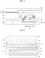
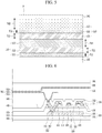
- FIG. 1 is a view schematically showing a display apparatus according to an embodiment of the present invention.
- FIG. 2 is an enlarged view of region P in FIG. 1 .
- the display apparatus may include a device substrate 100.
- the device substrate 100 may include an insulating material.
- the device substrate 100 may include a transparent material.
- the device substrate 100 may be a glass substrate.
- a light-emitting device 500 may be disposed on the device substrate 100.
- the light-emitting device 500 may emit light displaying a specific color.
- the light-emitting device 500 may include a first electrode 510, a light-emitting layer 520 and a second electrode 530, which are sequentially stacked.
- the first electrode 510 may include a conductive material.
- the first electrode 510 may include a transparent material.
- the first electrode 510 may be a transparent electrode formed of a transparent conductive material, such as ITO and IZO.
- An edge of the first electrode 510 may be covered by a bank insulating layer 150.
- the light-emitting layer 520 and the second electrode 530 may be stacked on a portion of the first electrode 510 which is exposed by the bank insulating layer 150.
- the plurality of the light-emitting devices 500 which are disposed on the device substrate 100 may be insulated by the bank insulating layer 150, each other.
- the light-emitting layer 520 may generate light having luminance corresponding to a voltage difference between the first electrode 510 and the second electrode 530.
- the light-emitting layer 520 may include an emission material layer (EML) having an emission material.
- the emission material may be an organic material, an inorganic material or a hybrid material.
- the display apparatus according to the embodiment of the present invention may be an organic light-emitting display apparatus including the light-emitting layer 520 formed of an organic material.
- the light-emitting layer 520 may have a multi-layer structure in order to increase luminous efficacy.
- the light-emitting layer 520 may further include at least one of a hole injection layer (HIL), a hole transporting layer (HTL), an electron transporting layer (ETL) and an electron injection layer (EIL).
- HIL hole injection layer
- HTL hole transporting layer
- ETL electron transporting layer
- EIL electron injection layer
- the second electrode 530 may include a conductive material.
- the second electrode 530 may include a material different from the first electrode 510.
- the second electrode 530 may include a metal having high reflectance, such as aluminum (Al) and silver (Ag).
- Al aluminum
- Ag silver
- a driving circuit may be disposed between the device substrate 100 and the light-emitting device 500.
- the driving circuit may supply a driving current to the light-emitting device 500.
- the driving circuit may include at least one thin film transistor 300 and a storage capacitor.
- the driving circuit may include the thin film transistor 300 which is electrically connected to the first electrode 510 of the light-emitting device 500.
- the thin film transistor 300 may generate the driving current according to a gate signal and a data signal.
- the thin film transistor 300 may include a semiconductor pattern 310, a gate insulating layer 320, a gate electrode 330, an interlayer insulating layer 340, a source electrode 350 and a drain electrode 360.
- the light-emitting device 500 may be connected to the drain electrode 360 of the corresponding thin film transistor 300.
- the semiconductor pattern 310 may be disposed close to the device substrate 100.
- the semiconductor pattern 310 may include a semiconductor material.
- the semiconductor pattern 310 may include amorphous silicon or poly-crystal silicon.
- the semiconductor pattern 310 may be oxide semiconductor.
- the semiconductor pattern 310 may include IGZO.
- the semiconductor pattern 310 may include a source region, a drain region and a channel region.
- the channel region may be disposed between the source region and the drain region.
- the channel region may have the conductivity lower than the source region and the drain region.
- the source region and the drain region may have the concentration of a conductive impurity higher than the channel region.
- the gate insulating layer 320 may be disposed on the semiconductor pattern 310. An upper surface of the semiconductor pattern 310 opposite to the device substrate 100 may be partially covered by the gate insulating layer 320. For example, the gate insulating layer 320 may overlap the channel region of the semiconductor pattern 310. The source region and the drain region of the semiconductor pattern 310 may be exposed by the gate insulating layer 320.
- the gate insulating layer 320 may include an insulating material.
- the gate insulating layer 320 may include silicon oxide and/or silicon nitride.
- the gate insulating layer 320 may include a High-K material.
- the gate insulating layer 320 may include hafnium oxide (HfO) or titanium oxide (TiO).
- the gate insulating layer 320 may have a multi-layer structure.
- the gate electrode 330 may be disposed on the gate insulating layer 320.
- the gate electrode 330 may be insulated from the semiconductor pattern 310 by the gate insulating layer 320.
- the gate electrode 330 may overlap the channel region of the semiconductor pattern 310.
- the gate electrode 330 may include a conductive material.
- the gate electrode 330 may include a metal, such as aluminum (Al), chrome (Cr), molybdenum (Mo) and tungsten (W).
- the interlayer insulating layer 340 may be disposed on the semiconductor pattern 310 and the gate electrode 330.
- the interlayer insulating layer 340 may be extended beyond the semiconductor pattern 310.
- a side surface of the semiconductor pattern 310 and a side surface of the gate electrode 330 may be covered by the interlayer insulating layer 340.
- the interlayer insulating layer 340 may include an insulating material.
- the refractive index of the interlayer insulating layer 340 may be the same as the refractive index of the device substrate 100.
- the interlayer insulating layer 340 may include silicon oxide.
- the source electrode 350 and the drain electrode 360 may be disposed on the interlayer insulating layer 340.
- the source electrode 350 may be electrically connected to the source region of the semiconductor pattern 310.
- the drain electrode 360 may be electrically connected to the drain region of the semiconductor pattern 310.
- the drain electrode 360 may be spaced away from the source electrode 350.
- the interlayer insulating layer 340 may include a contact hole exposing the source region of the semiconductor pattern 310, and a contact hole exposing the drain region of the semiconductor pattern 310.
- the source electrode 350 and the drain electrode 360 may include a conductive material.
- the source electrode 350 and the drain electrode 360 may include a metal, such as aluminum (Al), chrome (Cr), molybdenum (Mo) and tungsten (W).
- the drain electrode 360 may include the same material as the source electrode 350.
- the gate electrode 330 may include a material different from the source electrode 350 and the drain electrode 360.
- the driving circuit may not overlap the portion of the first electrode 510 exposed by the bank insulation layer 150.
- the thin film transistor 300 may overlap the bank insulating layer 150.
- the light emitted from the light-emitting device 500 may be not blocked by the thin film transistor 300.
- a buffer insulating layer may be disposed between the device substrate 100 and the thin film transistor 300.
- the buffer insulating layer may prevent the quality deterioration due to the device substrate 100 in the process of forming the thin film transistor 300 and the process of forming the light-emitting device 500.
- the buffer insulating layer may have a multi-layer structure.
- the buffer insulating layer may include a first buffer insulating layer 110 and a second buffer insulating layer 120, which are sequentially stacked.
- the buffer insulating layer may be disposed on the device substrate 100.
- the buffer insulating layer may prevent the quality deterioration due to the device substrate 100 in subsequent process.
- the buffer insulating layer may have a multi-layer structure.
- the buffer insulating layer may have a stacked structure in which a first buffer insulating layer 110 and a second buffer insulating layer 120 are stacked.
- the first buffer insulating layer 110 may be disposed close to the device substrate 100.
- the first buffer insulating layer 110 may be disposed between the device substrate 100 and the second buffer insulating layer 120.
- the refractive index of the first buffer insulating layer 110 may increase in a direction away from the device substrate 100.
- the first buffer insulating layer 110 may include first buffer layers 111, 112 and 113 having different refractive index.
- the first buffer insulating layer 110 may include a first lowest buffer layer 111, a first intermediate buffer layer 112 and a first highest buffer layer 113, which are sequentially stacked on the device substrate 100.
- the refractive index of the first highest buffer layer 113 may be larger than the refractive index of the first lowest buffer layer 111.
- the refractive index of the first intermediate buffer layer 112 may be between the refractive index of the first lowest buffer layer 111 and the refractive index of the first highest buffer layer 113.
- the refractive index of the first lowest buffer layer 111 may be larger than the refractive index of the device substrate 100.
- the first buffer layers 111, 112 and 113 may include an insulating material. At least one of the first buffer layers 111, 112 and 113 may include a different material.
- the first lowest buffer layer 111 and the first intermediate buffer layer 112 may include silicon oxynitride (SiON), and the first highest buffer layer 113 may include silicon nitride (SiN).
- the first buffer layers 111, 112 and 113 may have the same thickness.
- the thickness TC1 of the first intermediate buffer layer 112 may be the same as the thickness TL1 of the first lowest buffer layer 111.
- the thickness TU1 of the first highest buffer layer 113 may be the same as the thickness TC1 of the first intermediate buffer layer 112.
- the second buffer insulating layer 120 may be disposed on the first buffer insulating layer 110.
- the second buffer insulating layer 120 may be disposed between the first buffer insulating layer 110 and the light-emitting device 500.
- the second buffer insulating layer 120 may be in direct contact with an upper surface of the first buffer insulating layer 110 opposite to the device substrate 100.
- the upper surface of the first buffer insulating layer 110 may be an interface between the first buffer insulating layer 110 and the second buffer insulating layer 120.
- the refractive index of the second buffer insulating layer 120 may decrease in a direction away from the first buffer insulating layer 110. Thus, in the display apparatus according to the embodiment of the present invention, the steep change of the refractive index in a path of the light emitted from the light-emitting device 500 may be prevented.
- the second buffer insulating layer 120 may include second buffer layers 121, 122 and 123 having the different refractive index.
- the second buffer insulating layer 120 may include a second lowest buffer layer 121, a second intermediate buffer layer 122 and a second highest buffer layer 123, which are sequentially stacked on the first buffer insulating layer 110.
- the refractive index of the second highest buffer layer 123 may be smaller than the refractive index of the second lowest buffer layer 121.
- the refractive index of the second intermediate buffer layer 122 may be between the refractive index of the second lowest buffer layer 121 and the refractive index of the second highest buffer layer 123.
- the second buffer layers 121, 122 and 123 may include an insulating material. At least one of the second buffer layers 121, 122 and 123 may include a different material.
- the second lowest buffer layer 121 and the second intermediate buffer layer 122 may include silicon oxynitride (SiON), and the second highest buffer layer 123 may include silicon oxide (SiO).
- the variation of the refractive index between the second buffer layers 121, 122 and 123 may be different from the variation of the refractive index between the first buffer layers 111, 112 and 113 with respect to the interface between the first buffer insulating layer 110 and the second buffer insulating layer 120.
- the refractive index of the second lowest buffer layer 121 may be smaller than the refractive index of the first highest buffer layer 113.
- the refractive index of the second intermediate buffer layer 122 may be smaller than the refractive index of the first intermediate buffer layer 112.
- the refractive index of the second highest buffer layer 123 may be smaller than the refractive index of the first lowest buffer layer 111.
- the first buffer layers 111, 112 and 113 and the second buffer layers 121, 122 and 123 may have the refractive index symmetrical with respect to the first highest buffer layer 113.
- the refractive index of the second lowest buffer layer 121 may be the same as the refractive index of the first intermediate buffer layer 112.
- the thickness TL2 of the second lowest buffer layer 121 may be the same as the thickness TC1 of the first intermediate buffer layer 112.
- the refractive index of the second intermediate buffer layer 122 may be the same as the refractive index of the first lowest buffer layer 111.
- the thickness TC2 of the second intermediate buffer layer 122 may be the same as the thickness TL1 of the first lowest buffer layer 111.
- the refractive index of the second highest buffer layer 123 may be the same as the refractive index of the device substrate 100.
- the thickness TU2 of the second highest buffer layer 123 may be larger than the thickness TC2 of the second intermediate buffer layer 122.
- a light-blocking pattern 200 may be disposed between the device substrate 100 and the first buffer insulating layer 110.
- the light-blocking pattern 200 may block the light incident from the outside.
- the semiconductor pattern 310 of the thin film transistor 300 may overlap the light-blocking pattern 200.
- a horizontal width of the light-blocking pattern 200 may be larger than a horizontal width of the semiconductor pattern 310.
- the light-blocking pattern 200 may have a multi-layer structure.
- the light-blocking pattern 200 may include a low-reflective layer 210 and the light-blocking layer 220, which are sequentially stacked on the device substrate 100.
- the low-reflective layer 210 may include a low-reflective material.
- the low-reflective layer 210 may include a low-reflective metal, such as molybdenum (Mo), chrome (Cr), titanium (Ti) and tantalum (Ta).
- the light-blocking layer 220 may include a conductive material. The reflectance of the light-blocking layer 220 may be larger than the reflectance of the low-reflective layer 210.
- the light-blocking layer 220 may include a metal, such as aluminum (Al) and silver (Ag).
- a metal such as aluminum (Al) and silver (Ag).
- the light-blocking pattern 200 may be electrically connected to the driving circuit.
- the drain electrode 360 of the thin film transistor 300 may be connected to the light-blocking layer 220 of the light-blocking pattern 200.
- the first buffer insulating layer 110 and the second buffer insulating layer 120 may include a contact hole exposing a portion of the light-blocking layer 220.
- a lower passivation layer 130 may be disposed on an upper surface of the thin film transistor 300 opposite to the device substrate 100.
- the lower passivation layer 130 may prevent the damage of the thin film transistor 300 due to the external impact and moisture.
- the lower passivation layer 130 may be extended beyond the source electrode 350 and the drain electrode 360.
- the thin film transistor 300 may be covered by the lower passivation layer 130, substantially.
- the lower passivation layer 130 may include an insulating material.
- the lower passivation layer 130 may be direct contact with the interlayer insulating layer 340 on the outside of the source electrode 350 and the drain electrode 360.
- the lower passivation layer 130 may include the same material as the interlayer insulating layer 340.
- the lower passivation layer 130 may include silicon oxide.
- An over-coat layer 140 may be disposed between the lower passivation layer 130 and the light-emitting device 500, and between the lower passivation layer 130 and the bank insulating layer 150.
- the over-coat layer 140 may remove a thickness difference due to the light-blocking pattern 200 and the thin film transistor 300.
- an upper surface of the over-coat layer 140 opposite to the device substrate 100 may be a flat surface.
- the over-coat layer 140 may include an insulating material.
- the over-coat layer 140 may include a relative fluid material.
- the over-coat layer 140 may include an organic insulating material.
- a color filter 400 may be disposed on the path of the light emitted from the light-emitting device 500.
- the color filter 400 may be disposed between the lower passivation layer 130 and the over-coat layer 140.
- a thickness difference due to the color filter 400 may be removed by the over-coat layer 140.
- the color realized by the light which is emitted from the light-emitting device may be changed by the color filter 400.
- the light which is emitted from the light-emitting device 500 and displays white color may realize blue color, red color or green color by the color filter 400.
- the color filter 400 may overlap the portion of the first electrode 510 exposed by the bank insulating layer 150.
- the color filter 400 may not overlap the thin film transistor 300.
- a horizontal width of the color filter 400 may be larger than a horizontal width of the portion of the first electrode 510 exposed by the bank insulating layer 150.
- An encapsulating layer 600 may be disposed on the second electrode 530 of the light-emitting device 500.
- the encapsulating layer 600 may prevent the damage of the light-emitting device 500 due to the external impact and moisture.
- the encapsulating layer 600 may completely cover the light-emitting devices 500 which are disposed on the device substrate 100.
- the encapsulating layer 600 may include moisture-absorbing beads formed of a moisture-absorbing material.
- the encapsulating layer 600 may have a multi-layer structure.
- the encapsulating layer 600 may include a lower encapsulating layer and an upper encapsulating layer, which are sequentially stacked on the light-emitting device 500.
- the moisture-absorbing beads may be dispersed in the upper encapsulating layer.
- the lower encapsulating layer may be disposed between the light-emitting device 500 and the upper encapsulating layer.
- the stress applied to the light-emitting device 500 due to expansion of the moisture-absorbing beads may be relieved by the lower encapsulating layer.
- the encapsulating layer 600 may include an insulating material.
- the encapsulating layer 600 may include a material which does not need a curing process.
- the encapsulating layer 600 may include an olefin-based material.
- the lower encapsulating layer may include a material different from the upper encapsulating layer.
- the display apparatus is described as having the encapsulating layer 600 in direct contact with the light-emitting device 500.
- the display apparatus according to another embodiment of the present invention may further include an upper passivation layer between the second electrode 530 of the light-emitting device 500 and the encapsulating layer 600.
- the upper passivation layer may prevent the damage of the light-emitting device 500 due to the external impact and moisture.
- the upper passivation layer may include an insulating material.
- the upper passivation layer may have a multi-layer structure.
- the upper passivation layer may include a material different from the encapsulating layer 600.
- the upper passivation layer may have a structure in which an organic insulating layer formed of an organic material is disposed between inorganic insulating layers which are formed of an inorganic material.
- An encapsulation substrate 700 may be disposed on the encapsulating layer 600.
- the encapsulation substrate 700 may be coupled with the device substrate 100 on which the light-emitting device 500 is formed, by the encapsulating layer 600.
- the encapsulation substrate 700 may include a material different from the device substrate 100.
- the encapsulating substrate 700 may dissipate heat generated by the light-emitting device 500 and/or the thin film transistor 300 in the operation of realizing the image.
- the encapsulation substrate 700 may include a metal having a relatively high thermal conductivity, such as aluminum (Al).
- the display apparatus may include the first buffer insulating layer 110 and the second buffer insulating layer 120 which are stacked between the device substrate 100 and the light-emitting device 500.
- the first buffer insulating layer 110 may have the refractive index decreasing in a direction away from the light-emitting device 500.
- the second buffer insulating layer 120 may have the refractive index increasing in the direction away from the light-emitting device 500.
- the steep change of the refractive index between the buffer insulating layer and the peripheral element may be prevented.
- the unintended reflection due to the buffer insulating layer may be prevented.
- FIG. 3 is a graph displaying the spectrum of the light emitted from the light-emitting device 500 according to the distribution of the refractive index in the buffer insulating layer which is disposed between the device substrate 100 and the light-emitting device 500.
- S1 is a graph displaying the spectrum of the display apparatus according to the embodiment of the present invention.
- S2 is a graph displaying the spectrum of the display apparatus including the buffer insulating layer which has the refractive index decreasing in a direction toward the light-emitting device from the device substrate.
- S3 is a graph displaying the spectrum of the display apparatus including the buffer insulating layer which has the refractive index increasing in a direction toward the light-emitting device from the device substrate.
- the graph wiggling of S1 is smaller than the graph wiggling of S2 and S3. That is, the display apparatus according to the embodiment of the present invention may prevent the unintended constructive and destructive interference of the light emitted from the light-emitting device 500 by the stacked structure of the first buffer insulating layer 110 and the second buffer insulating layer 120, which have the refractive index decreasing in a direction away from the interface between the first buffer insulating layer 110 and the second buffer insulating layer 120.
- the characteristics distribution of the light according to the position may be prevented. Therefore, in the display apparatus according to the embodiment of the present invention, the luminous efficacy may be increased, and the variation of color coordinates may be prevented.
- the display apparatus according to the embodiment of the present invention is described under that assumption that the second lowest buffer layer 121 of the second buffer insulating layer 120 has the refractive index smaller than the first highest buffer layer 113 of the first buffer insulating layer 110.
- the variation of the refractive index between the second buffer layers 121, 122 and 123 may be symmetrical with the variation of the refractive index between the first buffer layers 111, 112 and 113 with respect to the interface between the first buffer insulating layer 110 and the second buffer insulating layer 120.
- the refractive index of the second lowest buffer layer 121, the second intermediate buffer layer 122 and the second highest buffer layer 123 of the second buffer insulating layer 120 may be the same as the refractive index of the first highest buffer layer 113, the first intermediate buffer layer 112 and the first lowest buffer layer 111 of the first buffer insulating layer 110, respectively.
- the thickness TU2 of the second highest buffer layer 123 may be the same as the thickness TL1 of the first lowest buffer layer 111
- the thickness TC2 of the second intermediate buffer layer 122 may be the same as the thickness TC1 of the first intermediate buffer layer 112
- the thickness TL2 of the second lowest buffer layer 121 may be the same as the thickness TU1 of the first highest buffer layer 113, as shown in FIG. 4 . Therefore, in the display apparatus according to another embodiment of the present invention, the wiggling of the spectrum may be minimized, and the quality deterioration due to the device substrate 100 may be efficiently prevented.
- the first buffer layers 111, 112 and 113 have different thicknesses. In other, words the thicknesses differ from each other.
- the thickness TL1 of the first lowest buffer layer 111 may be smaller than the thickness TU1 of the first highest buffer layer 113
- the thickness TC1 of the first intermediate buffer layer 112 may be between the thickness TL1 of the first lowest buffer layer 111 and the thickness TU1 of the first highest buffer layer 113, as shown in FIG. 5 .
- the second buffer layers 121, 122 and 123 may have the thickness corresponding to the first buffer layers 111, 112 and 113.
- the degree of freedom in the configuration of the buffer insulating layer may be improved.
- the thin film transistor 300 may include the gate electrode 330, the source electrode 350 and the drain electrode 360 which have a multi-layer structure, as shown in FIG. 6 .
- the gate electrode 330 may include a lower gate layer 331 and an upper gate layer 332
- the source electrode 350 may include a lower source layer 351 and an upper source layer 352
- the drain electrode 360 may include a lower drain layer 361 and an upper drain layer 362.
- the lower gate layer 331, the lower source layer 351 and the lower drain layer 361 may include a low-reflective material.
- the lower gate layer 331, the lower source layer 351 and the lower drain layer 361 may include a low-reflective metal, such as molybdenum (Mo), chrome (Cr), titanium (Ti) and tantalum (Ta).
- the upper gate layer 332, the upper source layer 352 and the upper drain layer 362 may have the conductivity higher than the lower gate layer 331, the lower source layer 351 and the lower drain layer 361, respectively.
- the display apparatus according to the embodiment of the present invention is described under the assumption that the interlayer insulating layer 340 of the thin film transistor 300 is extended between the second buffer insulating layer 120 and the lower passivation layer 130.
- the lower passivation layer 130 may be in direct contact with the second buffer insulating layer 120 between the device substrate 100 and the color filter 400, as shown in FIG. 6 .
- a portion of the interlayer insulating layer 340 may be removed by using a mask in the process of forming the source electrode 350 and the drain electrode 360.
- the degree of freedom in a material of the interlayer insulating layer 340 may be improved.
- the refractive index of the interlayer insulating layer 340 may be very different from the refractive index of the lower passivation layer 130.
- the function of the interlayer insulating layer 340 may be sufficiently performed, and the variation of the color coordinates may be prevented.
- each of the light-emitting devices 500 may include the light-emitting layer 520 separated from adjacent light-emitting devices 500, as shown in FIG. 7 .
- the light-emitting device 500 disposed on a blue sub-pixel may include a blue light-emitting layer 520
- the light-emitting device 500 disposed on a green sub-pixel may include a green light-emitting layer 520
- the light-emitting device 500 disposed on a red sub-pixel may include a red light-emitting layer 520.
- FIG. 8 is a graph displaying the spectrum of the light emitted from the light-emitting device on the blue sub-pixel according to the presence or absence of stacking the first buffer insulating layer and the second buffer insulating layer between the device substrate and the light-emitting device.
- FIG. 9 is a graph displaying the spectrum of the light emitted from the light-emitting device on the green sub-pixel according to the presence or absence of stacking the first buffer insulating layer and the second buffer insulating layer between the device substrate and the light-emitting device.
- FIG. 10 is a graph displaying the spectrum of the light emitted from the light-emitting device on the red sub-pixel according to the presence or absence of stacking the first buffer insulating layer and the second buffer insulating layer between the device substrate and the light-emitting device.
- the display apparatus B1, G1 and R1 including the first buffer insulating layer and the second buffer insulating layer which are stacked between the device substrate and the light-emitting device of the blue, green or red sub-pixel may have the wiggling of the graph smaller than the display apparatus B2, G2 and R2 including the buffer insulating layer having the specific refractive index. That is, in the display apparatus according to another embodiment of the present invention, the luminous efficacy of the light-emitting device having the light-emitting layer separated from adjacent light-emitting device may be increased, and the variation of the color coordinates due to constructive/destructive interference between the reflected lights may be prevented.
- the color coordinates may be optimized by adjusting the stacked structure of the first buffer insulating layer and the second buffer insulating layer of the display apparatus.
- the quality of the realized image may be improved.
- the display apparatus may prevent the steep change of the refractive index due to the buffer insulating layer which is disposed between the device substrate and the light-emitting device.
- the light emitted from the light-emitting device may not reflected by the difference of the refractive index between adjacent insulating layers. That is, in the display apparatus according to the embodiments of the present invention, the unintended constructive and destructive interference of the light may be prevented. Therefore, in the display apparatus according to the embodiments of the present invention, the luminous efficacy may be increased, and the variation of color coordinates may be prevented.
Landscapes
- Engineering & Computer Science (AREA)
- Microelectronics & Electronic Packaging (AREA)
- Physics & Mathematics (AREA)
- Optics & Photonics (AREA)
- Electroluminescent Light Sources (AREA)
- Devices For Indicating Variable Information By Combining Individual Elements (AREA)
Abstract
Description
- This application claims the priority benefit of Korean Patent Application No.
10-2018-0123316, filed on October 16, 2018 - The present invention relates to a display apparatus including insulating layers which are disposed on a path of light generated by a light-emitting device.
- Generally, an electronic appliance, such as a monitor, a TV, a laptop computer and a digital camera, includes a display apparatus to realize an image. For example, the display apparatus may include a light-emitting device which emits light to display a specific color, and a thin film transistor for controlling the light-emitting device.
- The thin film transistor and the light-emitting device may be formed on a device substrate. The device substrate may support the thin film transistor and the light-emitting device. The device substrate may include a transparent material. For example, the light emitted from the light-emitting device may emit outside through the device substrate.
- A buffer insulating layer may be disposed between the device substrate and the thin film transistor, and between the device substrate and the light-emitting device. The buffer insulating layer may prevent the quality deterioration due to the device substrate in the process of forming the light-emitting device.
- However, in the display apparatus, the light emitted from the light-emitting device may be reflected by the difference of the refractive index between the device substrate and the buffer insulating layer, and/or the difference of the refractive index of layers or elements between the device substrate and the light-emitting device, unintentionally. The light unintentionally reflected between the device substrate and the light-emitting device may be re-reflected by an electrode of the light-emitting device and/or an electrode of the thin film transistor. The light re-reflected by the electrode of the light-emitting device and/or the electrode of the thin film transistor may occur the constructive and/or destructive interference with the light which is not reflected between the device substrate and the light-emitting device. Thus, in the display apparatus, the luminance may be decreased or the color coordinates may be changed.
- Accordingly, the present invention is directed to a display apparatus that substantially obviates one or more problems due to limitations and disadvantages of the related art.
- An object of the present invention is to provide a display apparatus capable of preventing the unintended constructive and destructive interference of the light.
- Another object of the present invention is to provide a display apparatus capable of preventing the unintended reflection at the interface between insulating layers which are disposed on the path of the light emitted from the light-emitting device.
- Additional advantages, objects, and features of the invention will be set forth in part in the description which follows and in part will become apparent to those having ordinary skill in the art upon examination of the following or may be learned from practice of the invention. The objectives and other advantages of the invention may be realized and attained by the structure particularly pointed out in the written description and claims hereof as well as the appended drawings.
- To achieve these objects and other advantages and in accordance with the purpose of the invention, as embodied and broadly described herein, there is provided a display apparatus according to claim 1 and a display apparatus according to claim 13. Further embodiments are described in the dependent claims. According to an aspect of the present disclosure, a display apparatus includes a first buffer insulating layer on a device substrate. A second buffer insulating layer is disposed on the first buffer insulating layer. A light-emitting device is disposed on the second buffer insulating layer. The refractive index of the first buffer insulating layer and the refractive index of the second buffer insulating layer decrease in a direction away from an interface between the first buffer insulating layer and the second buffer insulating layer.
- A color filter may be disposed between the second buffer insulating layer and the light-emitting device.
- The first buffer insulating layer may include a first lowest buffer layer disposed close to the device substrate, a first highest buffer layer disposed close to the second buffer insulating layer, and a first intermediate buffer layer between the first lowest buffer layer and the first highest buffer layer. The refractive index of the first intermediate buffer layer may be between the refractive index of the first lowest buffer layer and the refractive index of the first highest buffer layer.
- The refractive index of the first lowest buffer layer may be larger than the refractive index of the device substrate.
- The second buffer insulating layer may include a second lowest buffer layer disposed close to the first buffer insulating layer. The refractive index of the second lowest buffer layer may be smaller than the refractive index of the first highest buffer layer.
- The refractive index of the second lowest buffer layer may be the same as the refractive index of the first intermediate buffer layer.
- The second buffer insulating layer may further include a second highest buffer layer disposed close to the light-emitting device, and a second intermediate buffer layer between the second lowest buffer layer and the second highest buffer layer. The refractive index of the second intermediate buffer layer may be between the refractive index of the second lowest buffer layer and the refractive index of the second highest buffer layer.
- The refractive index of the second intermediate buffer layer may be the same as the refractive index of the first lowest buffer layer.
- The refractive index of the second highest buffer layer may be the same as the refractive index of the device substrate.
- The thickness of the second highest buffer layer may be larger than the thickness of the second intermediate buffer layer.
- In accordance with another aspect of the present disclosure, a display apparatus includes a light-emitting device. The light-emitting device includes a first electrode, a second electrode and a light-emitting layer between the first electrode and the second electrode. A buffer insulating layer is disposed on the first electrode of the light-emitting device. The buffer insulating layer has a stacked structure of a first buffer insulating layer having a refractive index which decreases in a direction away from the light-emitting device, and a second buffer insulating layer having a refractive index which increases in a direction away from the light-emitting device.
- The second buffer insulating layer may be disposed between the light-emitting device and the first buffer insulating layer.
- The first buffer insulating layer may have a stacked structure of first buffer layers. The second buffer insulating layer may have a stacked structure of second buffer layers. The number of the stacked second buffer layers may be the same as the number of the stacked first buffer layers.
- The first buffer layers may have the same thickness.
- The variation of the refractive index between the second buffer layers may symmetrical with the variation of the refractive index between the first buffer layers.
- The accompanying drawings, which are included to provide a further understanding of the invention and are incorporated in and constitute a part of this application, illustrate embodiment(s) of the invention and together with the description serve to explain the principle of the invention. In the drawings:
-
FIG. 1 is a view schematically showing a display apparatus according to an embodiment of the present invention; -
FIG. 2 is an enlarged view of region P inFIG. 1 ; -
FIG. 3 is a graph displaying the spectrum of the light emitted from the light-emitting device according to the distribution of the refractive index in the buffer insulating layer which is disposed between the device substrate and the light-emitting device; -
FIGS. 4 to 7 are views respectively showing the display apparatus according to another embodiment of the present invention; -
FIGS. 8 to 10 are graphs respectively displaying the spectrum of the light emitted from the light-emitting device in the blue, green or red sub-pixel according to the presence or absence of stacking the first buffer insulating layer and the second buffer insulating layer between the device substrate and the light-emitting device. - Hereinafter, details related to the above objects, technical configurations, and operational effects of the embodiments of the present invention will be clearly understood by the following detailed description with reference to the drawings, which illustrate some embodiments of the present invention. Here, the embodiments of the present invention are provided in order to allow the technical sprit of the present invention to be satisfactorily transferred to those skilled in the art, and thus the present invention may be embodied in other forms and is not limited to the embodiments described below.
- In addition, the same or extremely similar elements may be designated by the same reference numerals throughout the specification, and in the drawings, the lengths and thickness of layers and regions may be exaggerated for convenience. It will be understood that, when a first element is referred to as being "on" a second element, although the first element may be disposed on the second element so as to come into contact with the second element, a third element may be interposed between the first element and the second element.
- Here, terms such as, for example, "first" and "second" may be used to distinguish any one element with another element. However, the first element and the second element may be arbitrary named according to the convenience of those skilled in the art without departing the technical sprit of the present invention.
- The terms used in the specification of the present invention are merely used in order to describe particular embodiments, and are not intended to limit the scope of the present invention. For example, an element described in the singular form is intended to include a plurality of elements unless the context clearly indicates otherwise. In addition, in the specification of the present invention, it will be further understood that the terms "comprises" and "includes" specify the presence of stated features, integers, steps, operations, elements, components, and/or combinations thereof, but do not preclude the presence or addition of one or more other features, integers, steps, operations, elements, components, and/or combinations.
- Unless otherwise defined, all terms (including technical and scientific terms) used herein have the same meaning as commonly understood by one of ordinary skill in the art to which example embodiments belong. It will be further understood that terms, such as those defined in commonly used dictionaries, should be interpreted as having a meaning that is consistent with their meaning in the context of the relevant art and should not be interpreted in an idealized or overly formal sense unless expressly so defined herein.
-
FIG. 1 is a view schematically showing a display apparatus according to an embodiment of the present invention.FIG. 2 is an enlarged view of region P inFIG. 1 . - Referring to
FIGS. 1 and 2 , the display apparatus according to the embodiment of the present invention may include adevice substrate 100. Thedevice substrate 100 may include an insulating material. Thedevice substrate 100 may include a transparent material. For example, thedevice substrate 100 may be a glass substrate. - A light-emitting
device 500 may be disposed on thedevice substrate 100. The light-emittingdevice 500 may emit light displaying a specific color. For example, the light-emittingdevice 500 may include afirst electrode 510, a light-emittinglayer 520 and asecond electrode 530, which are sequentially stacked. - The
first electrode 510 may include a conductive material. Thefirst electrode 510 may include a transparent material. For example, thefirst electrode 510 may be a transparent electrode formed of a transparent conductive material, such as ITO and IZO. - An edge of the
first electrode 510 may be covered by abank insulating layer 150. The light-emittinglayer 520 and thesecond electrode 530 may be stacked on a portion of thefirst electrode 510 which is exposed by thebank insulating layer 150. Thus, in the display apparatus according to the embodiment of the present invention, the plurality of the light-emittingdevices 500 which are disposed on thedevice substrate 100 may be insulated by thebank insulating layer 150, each other. - The light-emitting
layer 520 may generate light having luminance corresponding to a voltage difference between thefirst electrode 510 and thesecond electrode 530. For example, the light-emittinglayer 520 may include an emission material layer (EML) having an emission material. The emission material may be an organic material, an inorganic material or a hybrid material. For example, the display apparatus according to the embodiment of the present invention may be an organic light-emitting display apparatus including the light-emittinglayer 520 formed of an organic material. - The light-emitting
layer 520 may have a multi-layer structure in order to increase luminous efficacy. For example, the light-emittinglayer 520 may further include at least one of a hole injection layer (HIL), a hole transporting layer (HTL), an electron transporting layer (ETL) and an electron injection layer (EIL). - The
second electrode 530 may include a conductive material. Thesecond electrode 530 may include a material different from thefirst electrode 510. For example, thesecond electrode 530 may include a metal having high reflectance, such as aluminum (Al) and silver (Ag). Thus, in the display apparatus according to the embodiment of the present invention, the light generated by the light-emittinglayer 520 may be emitted to outside through thefirst electrode 510 and thedevice substrate 100. - A driving circuit may be disposed between the
device substrate 100 and the light-emittingdevice 500. The driving circuit may supply a driving current to the light-emittingdevice 500. The driving circuit may include at least onethin film transistor 300 and a storage capacitor. For example, the driving circuit may include thethin film transistor 300 which is electrically connected to thefirst electrode 510 of the light-emittingdevice 500. - The
thin film transistor 300 may generate the driving current according to a gate signal and a data signal. For example, thethin film transistor 300 may include asemiconductor pattern 310, agate insulating layer 320, agate electrode 330, aninterlayer insulating layer 340, asource electrode 350 and adrain electrode 360. The light-emittingdevice 500 may be connected to thedrain electrode 360 of the correspondingthin film transistor 300. - The
semiconductor pattern 310 may be disposed close to thedevice substrate 100. Thesemiconductor pattern 310 may include a semiconductor material. For example, thesemiconductor pattern 310 may include amorphous silicon or poly-crystal silicon. Thesemiconductor pattern 310 may be oxide semiconductor. For example, thesemiconductor pattern 310 may include IGZO. - The
semiconductor pattern 310 may include a source region, a drain region and a channel region. The channel region may be disposed between the source region and the drain region. The channel region may have the conductivity lower than the source region and the drain region. For example, the source region and the drain region may have the concentration of a conductive impurity higher than the channel region. - The
gate insulating layer 320 may be disposed on thesemiconductor pattern 310. An upper surface of thesemiconductor pattern 310 opposite to thedevice substrate 100 may be partially covered by thegate insulating layer 320. For example, thegate insulating layer 320 may overlap the channel region of thesemiconductor pattern 310. The source region and the drain region of thesemiconductor pattern 310 may be exposed by thegate insulating layer 320. - The
gate insulating layer 320 may include an insulating material. For example, thegate insulating layer 320 may include silicon oxide and/or silicon nitride. Thegate insulating layer 320 may include a High-K material. For example, thegate insulating layer 320 may include hafnium oxide (HfO) or titanium oxide (TiO). Thegate insulating layer 320 may have a multi-layer structure. - The
gate electrode 330 may be disposed on thegate insulating layer 320. Thegate electrode 330 may be insulated from thesemiconductor pattern 310 by thegate insulating layer 320. For example, thegate electrode 330 may overlap the channel region of thesemiconductor pattern 310. - The
gate electrode 330 may include a conductive material. For example, thegate electrode 330 may include a metal, such as aluminum (Al), chrome (Cr), molybdenum (Mo) and tungsten (W). - The interlayer insulating
layer 340 may be disposed on thesemiconductor pattern 310 and thegate electrode 330. The interlayer insulatinglayer 340 may be extended beyond thesemiconductor pattern 310. For example, a side surface of thesemiconductor pattern 310 and a side surface of thegate electrode 330 may be covered by theinterlayer insulating layer 340. - The interlayer insulating
layer 340 may include an insulating material. The refractive index of the interlayer insulatinglayer 340 may be the same as the refractive index of thedevice substrate 100. For example, theinterlayer insulating layer 340 may include silicon oxide. - The
source electrode 350 and thedrain electrode 360 may be disposed on theinterlayer insulating layer 340. Thesource electrode 350 may be electrically connected to the source region of thesemiconductor pattern 310. Thedrain electrode 360 may be electrically connected to the drain region of thesemiconductor pattern 310. Thedrain electrode 360 may be spaced away from thesource electrode 350. For example, theinterlayer insulating layer 340 may include a contact hole exposing the source region of thesemiconductor pattern 310, and a contact hole exposing the drain region of thesemiconductor pattern 310. - The
source electrode 350 and thedrain electrode 360 may include a conductive material. For example, thesource electrode 350 and thedrain electrode 360 may include a metal, such as aluminum (Al), chrome (Cr), molybdenum (Mo) and tungsten (W). Thedrain electrode 360 may include the same material as thesource electrode 350. Thegate electrode 330 may include a material different from thesource electrode 350 and thedrain electrode 360. - The driving circuit may not overlap the portion of the
first electrode 510 exposed by thebank insulation layer 150. For example, thethin film transistor 300 may overlap thebank insulating layer 150. Thus, in the display apparatus according to the embodiment of the present invention, the light emitted from the light-emittingdevice 500 may be not blocked by thethin film transistor 300. - A buffer insulating layer may be disposed between the
device substrate 100 and thethin film transistor 300. The buffer insulating layer may prevent the quality deterioration due to thedevice substrate 100 in the process of forming thethin film transistor 300 and the process of forming the light-emittingdevice 500. The buffer insulating layer may have a multi-layer structure. For example, the buffer insulating layer may include a firstbuffer insulating layer 110 and a secondbuffer insulating layer 120, which are sequentially stacked. - The buffer insulating layer may be disposed on the
device substrate 100. The buffer insulating layer may prevent the quality deterioration due to thedevice substrate 100 in subsequent process. The buffer insulating layer may have a multi-layer structure. For example, the buffer insulating layer may have a stacked structure in which a firstbuffer insulating layer 110 and a secondbuffer insulating layer 120 are stacked. - The first
buffer insulating layer 110 may be disposed close to thedevice substrate 100. For example, the firstbuffer insulating layer 110 may be disposed between thedevice substrate 100 and the secondbuffer insulating layer 120. - The refractive index of the first
buffer insulating layer 110 may increase in a direction away from thedevice substrate 100. The firstbuffer insulating layer 110 may include first buffer layers 111, 112 and 113 having different refractive index. For example, the firstbuffer insulating layer 110 may include a firstlowest buffer layer 111, a firstintermediate buffer layer 112 and a firsthighest buffer layer 113, which are sequentially stacked on thedevice substrate 100. The refractive index of the firsthighest buffer layer 113 may be larger than the refractive index of the firstlowest buffer layer 111. The refractive index of the firstintermediate buffer layer 112 may be between the refractive index of the firstlowest buffer layer 111 and the refractive index of the firsthighest buffer layer 113. Also, the refractive index of the firstlowest buffer layer 111 may be larger than the refractive index of thedevice substrate 100. - The first buffer layers 111, 112 and 113 may include an insulating material. At least one of the first buffer layers 111, 112 and 113 may include a different material. For example, the first
lowest buffer layer 111 and the firstintermediate buffer layer 112 may include silicon oxynitride (SiON), and the firsthighest buffer layer 113 may include silicon nitride (SiN). - The first buffer layers 111, 112 and 113 may have the same thickness. For example, the thickness TC1 of the first
intermediate buffer layer 112 may be the same as the thickness TL1 of the firstlowest buffer layer 111. The thickness TU1 of the firsthighest buffer layer 113 may be the same as the thickness TC1 of the firstintermediate buffer layer 112. - The second
buffer insulating layer 120 may be disposed on the firstbuffer insulating layer 110. For example, the secondbuffer insulating layer 120 may be disposed between the firstbuffer insulating layer 110 and the light-emittingdevice 500. The secondbuffer insulating layer 120 may be in direct contact with an upper surface of the firstbuffer insulating layer 110 opposite to thedevice substrate 100. The upper surface of the firstbuffer insulating layer 110 may be an interface between the firstbuffer insulating layer 110 and the secondbuffer insulating layer 120. - The refractive index of the second
buffer insulating layer 120 may decrease in a direction away from the firstbuffer insulating layer 110. Thus, in the display apparatus according to the embodiment of the present invention, the steep change of the refractive index in a path of the light emitted from the light-emittingdevice 500 may be prevented. The secondbuffer insulating layer 120 may include second buffer layers 121, 122 and 123 having the different refractive index. For example, the secondbuffer insulating layer 120 may include a secondlowest buffer layer 121, a secondintermediate buffer layer 122 and a secondhighest buffer layer 123, which are sequentially stacked on the firstbuffer insulating layer 110. The refractive index of the secondhighest buffer layer 123 may be smaller than the refractive index of the secondlowest buffer layer 121. The refractive index of the secondintermediate buffer layer 122 may be between the refractive index of the secondlowest buffer layer 121 and the refractive index of the secondhighest buffer layer 123. - The second buffer layers 121, 122 and 123 may include an insulating material. At least one of the second buffer layers 121, 122 and 123 may include a different material. For example, the second
lowest buffer layer 121 and the secondintermediate buffer layer 122 may include silicon oxynitride (SiON), and the secondhighest buffer layer 123 may include silicon oxide (SiO). - The variation of the refractive index between the second buffer layers 121, 122 and 123 may be different from the variation of the refractive index between the first buffer layers 111, 112 and 113 with respect to the interface between the first
buffer insulating layer 110 and the secondbuffer insulating layer 120. For example, the refractive index of the secondlowest buffer layer 121 may be smaller than the refractive index of the firsthighest buffer layer 113. The refractive index of the secondintermediate buffer layer 122 may be smaller than the refractive index of the firstintermediate buffer layer 112. The refractive index of the secondhighest buffer layer 123 may be smaller than the refractive index of the firstlowest buffer layer 111. - The first buffer layers 111, 112 and 113 and the second buffer layers 121, 122 and 123 may have the refractive index symmetrical with respect to the first
highest buffer layer 113. For example, the refractive index of the secondlowest buffer layer 121 may be the same as the refractive index of the firstintermediate buffer layer 112. The thickness TL2 of the secondlowest buffer layer 121 may be the same as the thickness TC1 of the firstintermediate buffer layer 112. The refractive index of the secondintermediate buffer layer 122 may be the same as the refractive index of the firstlowest buffer layer 111. The thickness TC2 of the secondintermediate buffer layer 122 may be the same as the thickness TL1 of the firstlowest buffer layer 111. The refractive index of the secondhighest buffer layer 123 may be the same as the refractive index of thedevice substrate 100. The thickness TU2 of the secondhighest buffer layer 123 may be larger than the thickness TC2 of the secondintermediate buffer layer 122. - A light-blocking
pattern 200 may be disposed between thedevice substrate 100 and the firstbuffer insulating layer 110. The light-blockingpattern 200 may block the light incident from the outside. For example, thesemiconductor pattern 310 of thethin film transistor 300 may overlap the light-blockingpattern 200. A horizontal width of the light-blockingpattern 200 may be larger than a horizontal width of thesemiconductor pattern 310. Thus, in the display apparatus according to the embodiment of the present invention, an external light toward the channel region of thesemiconductor pattern 310 may be blocked by the light-blockingpattern 200. Therefore, in the display apparatus according to the embodiment of the present invention, the malfunction of thethin film transistor 300 due to the external light may be prevented. - The light-blocking
pattern 200 may have a multi-layer structure. For example, the light-blockingpattern 200 may include a low-reflective layer 210 and the light-blocking layer 220, which are sequentially stacked on thedevice substrate 100. The low-reflective layer 210 may include a low-reflective material. For example, the low-reflective layer 210 may include a low-reflective metal, such as molybdenum (Mo), chrome (Cr), titanium (Ti) and tantalum (Ta). The light-blocking layer 220 may include a conductive material. The reflectance of the light-blocking layer 220 may be larger than the reflectance of the low-reflective layer 210. For example, the light-blocking layer 220 may include a metal, such as aluminum (Al) and silver (Ag). Thus, in the display apparatus according to the embodiment of the present invention, the visibility deterioration due to the light reflected by the light-blocking layer 220 may be prevented. - The light-blocking
pattern 200 may be electrically connected to the driving circuit. For example, thedrain electrode 360 of thethin film transistor 300 may be connected to the light-blocking layer 220 of the light-blockingpattern 200. The firstbuffer insulating layer 110 and the secondbuffer insulating layer 120 may include a contact hole exposing a portion of the light-blocking layer 220. Thus, in the display apparatus according to the embodiment of the present invention, the parasitic capacitance due to the light-blockingpattern 200 may be prevented. - A
lower passivation layer 130 may be disposed on an upper surface of thethin film transistor 300 opposite to thedevice substrate 100. Thelower passivation layer 130 may prevent the damage of thethin film transistor 300 due to the external impact and moisture. For example, thelower passivation layer 130 may be extended beyond thesource electrode 350 and thedrain electrode 360. Thethin film transistor 300 may be covered by thelower passivation layer 130, substantially. - The
lower passivation layer 130 may include an insulating material. Thelower passivation layer 130 may be direct contact with the interlayer insulatinglayer 340 on the outside of thesource electrode 350 and thedrain electrode 360. Thelower passivation layer 130 may include the same material as theinterlayer insulating layer 340. For example, thelower passivation layer 130 may include silicon oxide. - An
over-coat layer 140 may be disposed between thelower passivation layer 130 and the light-emittingdevice 500, and between thelower passivation layer 130 and thebank insulating layer 150. Theover-coat layer 140 may remove a thickness difference due to the light-blockingpattern 200 and thethin film transistor 300. For example, an upper surface of theover-coat layer 140 opposite to thedevice substrate 100 may be a flat surface. - The
over-coat layer 140 may include an insulating material. Theover-coat layer 140 may include a relative fluid material. For example, theover-coat layer 140 may include an organic insulating material. - A
color filter 400 may be disposed on the path of the light emitted from the light-emittingdevice 500. For example, thecolor filter 400 may be disposed between thelower passivation layer 130 and theover-coat layer 140. A thickness difference due to thecolor filter 400 may be removed by theover-coat layer 140. - The color realized by the light which is emitted from the light-emitting device may be changed by the
color filter 400. For example, the light which is emitted from the light-emittingdevice 500 and displays white color may realize blue color, red color or green color by thecolor filter 400. Thecolor filter 400 may overlap the portion of thefirst electrode 510 exposed by thebank insulating layer 150. Thecolor filter 400 may not overlap thethin film transistor 300. A horizontal width of thecolor filter 400 may be larger than a horizontal width of the portion of thefirst electrode 510 exposed by thebank insulating layer 150. Thus, in the display apparatus according to the embodiment of the present invention, all of the light emitted from the light-emittingdevice 500 may pass through thecolor filter 400. Therefore, in the display apparatus according to the embodiment of the present invention, the light leakage may be prevented. - An
encapsulating layer 600 may be disposed on thesecond electrode 530 of the light-emittingdevice 500. Theencapsulating layer 600 may prevent the damage of the light-emittingdevice 500 due to the external impact and moisture. For example, theencapsulating layer 600 may completely cover the light-emittingdevices 500 which are disposed on thedevice substrate 100. Theencapsulating layer 600 may include moisture-absorbing beads formed of a moisture-absorbing material. Theencapsulating layer 600 may have a multi-layer structure. For example, theencapsulating layer 600 may include a lower encapsulating layer and an upper encapsulating layer, which are sequentially stacked on the light-emittingdevice 500. The moisture-absorbing beads may be dispersed in the upper encapsulating layer. The lower encapsulating layer may be disposed between the light-emittingdevice 500 and the upper encapsulating layer. Thus, in the display apparatus according to the embodiment of the present invention, the stress applied to the light-emittingdevice 500 due to expansion of the moisture-absorbing beads may be relieved by the lower encapsulating layer. - The
encapsulating layer 600 may include an insulating material. Theencapsulating layer 600 may include a material which does not need a curing process. For example, theencapsulating layer 600 may include an olefin-based material. Thus, in the display apparatus according to the embodiment of the present invention, the deterioration of the light-emittingdevice 500 due to the process of forming theencapsulating layer 600 may be prevented. The lower encapsulating layer may include a material different from the upper encapsulating layer. - The display apparatus according to the embodiment of the present invention is described as having the
encapsulating layer 600 in direct contact with the light-emittingdevice 500. However, the display apparatus according to another embodiment of the present invention may further include an upper passivation layer between thesecond electrode 530 of the light-emittingdevice 500 and theencapsulating layer 600. The upper passivation layer may prevent the damage of the light-emittingdevice 500 due to the external impact and moisture. The upper passivation layer may include an insulating material. The upper passivation layer may have a multi-layer structure. The upper passivation layer may include a material different from theencapsulating layer 600. For example, the upper passivation layer may have a structure in which an organic insulating layer formed of an organic material is disposed between inorganic insulating layers which are formed of an inorganic material. Thus, in the display apparatus according to another embodiment of the present invention, the damage of the light-emittingdevice 500 due to the external impact and moisture may be efficiently prevented. - An
encapsulation substrate 700 may be disposed on theencapsulating layer 600. Theencapsulation substrate 700 may be coupled with thedevice substrate 100 on which the light-emittingdevice 500 is formed, by theencapsulating layer 600. Theencapsulation substrate 700 may include a material different from thedevice substrate 100. The encapsulatingsubstrate 700 may dissipate heat generated by the light-emittingdevice 500 and/or thethin film transistor 300 in the operation of realizing the image. For example, theencapsulation substrate 700 may include a metal having a relatively high thermal conductivity, such as aluminum (Al). - Accordingly, the display apparatus according to the embodiment of the present invention may include the first
buffer insulating layer 110 and the secondbuffer insulating layer 120 which are stacked between thedevice substrate 100 and the light-emittingdevice 500. The firstbuffer insulating layer 110 may have the refractive index decreasing in a direction away from the light-emittingdevice 500. The secondbuffer insulating layer 120 may have the refractive index increasing in the direction away from the light-emittingdevice 500. Thus, in the display apparatus according to the embodiment of the present invention, the difference of the refractive index between insulating layers which are stacked on the path of the light emitted to the outside through thedevice substrate 100 may be minimized. Therefore, in the display apparatus according to the embodiment of the present invent, the steep change of the refractive index between the buffer insulating layer and the peripheral element may be prevented. Thereby, in the display apparatus according to the embodiment of the present invention, the unintended reflection due to the buffer insulating layer may be prevented. -
FIG. 3 is a graph displaying the spectrum of the light emitted from the light-emittingdevice 500 according to the distribution of the refractive index in the buffer insulating layer which is disposed between thedevice substrate 100 and the light-emittingdevice 500. Herein, S1 is a graph displaying the spectrum of the display apparatus according to the embodiment of the present invention. S2 is a graph displaying the spectrum of the display apparatus including the buffer insulating layer which has the refractive index decreasing in a direction toward the light-emitting device from the device substrate. S3 is a graph displaying the spectrum of the display apparatus including the buffer insulating layer which has the refractive index increasing in a direction toward the light-emitting device from the device substrate. - Referring to
FIG. 3 , the graph wiggling of S1 is smaller than the graph wiggling of S2 and S3. That is, the display apparatus according to the embodiment of the present invention may prevent the unintended constructive and destructive interference of the light emitted from the light-emittingdevice 500 by the stacked structure of the firstbuffer insulating layer 110 and the secondbuffer insulating layer 120, which have the refractive index decreasing in a direction away from the interface between the firstbuffer insulating layer 110 and the secondbuffer insulating layer 120. Thus, in the display apparatus according to the embodiment of the present invention, the characteristics distribution of the light according to the position may be prevented. Therefore, in the display apparatus according to the embodiment of the present invention, the luminous efficacy may be increased, and the variation of color coordinates may be prevented. - The display apparatus according to the embodiment of the present invention is described under that assumption that the second
lowest buffer layer 121 of the secondbuffer insulating layer 120 has the refractive index smaller than the firsthighest buffer layer 113 of the firstbuffer insulating layer 110. However, in the display apparatus according to another embodiment of the present invention, the variation of the refractive index between the second buffer layers 121, 122 and 123 may be symmetrical with the variation of the refractive index between the first buffer layers 111, 112 and 113 with respect to the interface between the firstbuffer insulating layer 110 and the secondbuffer insulating layer 120. For example, in the display apparatus according to another embodiment of the present invention, the refractive index of the secondlowest buffer layer 121, the secondintermediate buffer layer 122 and the secondhighest buffer layer 123 of the secondbuffer insulating layer 120 may be the same as the refractive index of the firsthighest buffer layer 113, the firstintermediate buffer layer 112 and the firstlowest buffer layer 111 of the firstbuffer insulating layer 110, respectively. Thus, in the display apparatus according to another embodiment of the present invention, the thickness TU2 of the secondhighest buffer layer 123 may be the same as the thickness TL1 of the firstlowest buffer layer 111, the thickness TC2 of the secondintermediate buffer layer 122 may be the same as the thickness TC1 of the firstintermediate buffer layer 112, and the thickness TL2 of the secondlowest buffer layer 121 may be the same as the thickness TU1 of the firsthighest buffer layer 113, as shown inFIG. 4 . Therefore, in the display apparatus according to another embodiment of the present invention, the wiggling of the spectrum may be minimized, and the quality deterioration due to thedevice substrate 100 may be efficiently prevented. - The display apparatus according to the embodiment of the present invention is described under the assumption that the first buffer layers 111, 112 and 113 have the same thickness (TL1=TC1=TU1). However, in the display apparatus according to another embodiment of the present invention, the first buffer layers 111, 112 and 113 have different thicknesses. In other, words the thicknesses differ from each other. For example, in the display apparatus according to another embodiment of the present invention, the thickness TL1 of the first
lowest buffer layer 111 may be smaller than the thickness TU1 of the firsthighest buffer layer 113, the thickness TC1 of the firstintermediate buffer layer 112 may be between the thickness TL1 of the firstlowest buffer layer 111 and the thickness TU1 of the firsthighest buffer layer 113, as shown inFIG. 5 . Also, in the display apparatus according to another embodiment of the present invention, the second buffer layers 121, 122 and 123 may have the thickness corresponding to the first buffer layers 111, 112 and 113. Thus, in the display apparatus according to another embodiment of the present invention, the degree of freedom in the configuration of the buffer insulating layer may be improved. - The display apparatus according to the embodiment of the present invention is described under the assumption that the
gate electrode 330, thesource electrode 350 and thedrain electrode 360 of thethin film transistor 300 have a single layer structure. However, in the display apparatus according to another embodiment of the present invention, thethin film transistor 300 may include thegate electrode 330, thesource electrode 350 and thedrain electrode 360 which have a multi-layer structure, as shown inFIG. 6 . For example, thegate electrode 330 may include alower gate layer 331 and anupper gate layer 332, thesource electrode 350 may include alower source layer 351 and anupper source layer 352, and thedrain electrode 360 may include alower drain layer 361 and anupper drain layer 362. Thelower gate layer 331, thelower source layer 351 and thelower drain layer 361 may include a low-reflective material. For example, thelower gate layer 331, thelower source layer 351 and thelower drain layer 361 may include a low-reflective metal, such as molybdenum (Mo), chrome (Cr), titanium (Ti) and tantalum (Ta). Theupper gate layer 332, theupper source layer 352 and theupper drain layer 362 may have the conductivity higher than thelower gate layer 331, thelower source layer 351 and thelower drain layer 361, respectively. - The display apparatus according to the embodiment of the present invention is described under the assumption that the interlayer insulating
layer 340 of thethin film transistor 300 is extended between the secondbuffer insulating layer 120 and thelower passivation layer 130. However, in the display apparatus according to another embodiment of the present invention, thelower passivation layer 130 may be in direct contact with the secondbuffer insulating layer 120 between thedevice substrate 100 and thecolor filter 400, as shown inFIG. 6 . For example, in the display apparatus according to another embodiment of the present invention, a portion of the interlayer insulatinglayer 340 may be removed by using a mask in the process of forming thesource electrode 350 and thedrain electrode 360. Thus, in the display apparatus according to another embodiment of the present invention, the degree of freedom in a material of the interlayer insulatinglayer 340 may be improved. For example, in the display apparatus according to another embodiment of the present invention, the refractive index of the interlayer insulatinglayer 340 may be very different from the refractive index of thelower passivation layer 130. Thus, in the display apparatus according to another embodiment of the present invention, the function of the interlayer insulatinglayer 340 may be sufficiently performed, and the variation of the color coordinates may be prevented. - The display apparatus according to the embodiment of the present invention is described under the assumption that the light-emitting
layer 520 and thesecond electrode 530 of the light-emittingdevice 500 may be extended onto thebank insulating layer 150. That is, in the display apparatus according to the embodiment of the present invention, the light-emittinglayer 520 of each light-emittingdevice 500 may be connected to the light-emittinglayer 520 of adjacent light-emittingdevice 500. However, in the display apparatus according to another embodiment of the present invention, each of the light-emittingdevices 500 may include the light-emittinglayer 520 separated from adjacent light-emittingdevices 500, as shown inFIG. 7 . For example, in the display apparatus according to another embodiment of the present invention, the light-emittingdevice 500 disposed on a blue sub-pixel may include a blue light-emittinglayer 520, the light-emittingdevice 500 disposed on a green sub-pixel may include a green light-emittinglayer 520, and the light-emittingdevice 500 disposed on a red sub-pixel may include a red light-emittinglayer 520. -
FIG. 8 is a graph displaying the spectrum of the light emitted from the light-emitting device on the blue sub-pixel according to the presence or absence of stacking the first buffer insulating layer and the second buffer insulating layer between the device substrate and the light-emitting device.FIG. 9 is a graph displaying the spectrum of the light emitted from the light-emitting device on the green sub-pixel according to the presence or absence of stacking the first buffer insulating layer and the second buffer insulating layer between the device substrate and the light-emitting device.FIG. 10 is a graph displaying the spectrum of the light emitted from the light-emitting device on the red sub-pixel according to the presence or absence of stacking the first buffer insulating layer and the second buffer insulating layer between the device substrate and the light-emitting device. - Referring to
FIGS. 9-10 , the display apparatus B1, G1 and R1 including the first buffer insulating layer and the second buffer insulating layer which are stacked between the device substrate and the light-emitting device of the blue, green or red sub-pixel may have the wiggling of the graph smaller than the display apparatus B2, G2 and R2 including the buffer insulating layer having the specific refractive index. That is, in the display apparatus according to another embodiment of the present invention, the luminous efficacy of the light-emitting device having the light-emitting layer separated from adjacent light-emitting device may be increased, and the variation of the color coordinates due to constructive/destructive interference between the reflected lights may be prevented. For example, in the display apparatus according to another embodiment of the present invention, the color coordinates may be optimized by adjusting the stacked structure of the first buffer insulating layer and the second buffer insulating layer of the display apparatus. Thus, in the display apparatus according to another embodiment of the present invention, the quality of the realized image may be improved. - In the result, the display apparatus according to the embodiments of the present invention may prevent the steep change of the refractive index due to the buffer insulating layer which is disposed between the device substrate and the light-emitting device. Thus, in the display apparatus according to the embodiments of the present invention, the light emitted from the light-emitting device may not reflected by the difference of the refractive index between adjacent insulating layers. That is, in the display apparatus according to the embodiments of the present invention, the unintended constructive and destructive interference of the light may be prevented. Therefore, in the display apparatus according to the embodiments of the present invention, the luminous efficacy may be increased, and the variation of color coordinates may be prevented.
Claims (15)
- A display apparatus comprising:a device substrate (100);a first buffer insulating layer (110) on the device substrate (100);a second buffer insulating layer (120) on the first buffer insulating layer (110); anda light-emitting device (500) on the second buffer insulating layer (120),wherein the refractive index of the first buffer insulating layer (110) and the refractive index of the second buffer insulating layer (120) decrease in a direction away from the interface between the first buffer insulating layer (110) and the second buffer insulating layer (120).
- The display apparatus according to claim 1, wherein the first buffer insulating layer (110) includes a first lowest buffer layer (111) disposed on the device substrate (100), a first intermediate buffer layer (112) disposed on the first lowest buffer layer (111), and a first highest buffer layer (113) disposed on the first intermediate buffer layer (112),
wherein the refractive index of the first intermediate buffer layer (112) is between the refractive index of the first lowest buffer layer (111) and the refractive index of the first highest buffer layer (113). - The display apparatus according to claim 2, wherein the refractive index of the first lowest buffer layer (111) is larger than the refractive index of the device substrate (100) .
- The display apparatus according to claim 2 or 3, wherein the first lowest buffer layer (111), the first intermediate buffer layer (112) and the first highest buffer layer (113) have the same thickness.
- The display apparatus according to any one of claims 2 to 4, wherein the second buffer insulating layer (120) includes a second lowest buffer layer (121) disposed on the first buffer insulating layer (110), and
wherein the refractive index of the second lowest buffer layer (121) is smaller than the refractive index of the first highest buffer layer (113). - The display apparatus according to claim 5, wherein the refractive index of the second lowest buffer layer (121) is the same as the refractive index of the first intermediate buffer layer (112).
- The display apparatus according to claim 5 or 6, wherein the second buffer insulating layer (120) further includes a second intermediate buffer layer (122) disposed on the second lowest buffer layer (121), and a second highest buffer layer (123) disposed on the second intermediate buffer layer (122),
wherein the refractive index of the second intermediate buffer layer (122) is between the refractive index of the second lowest buffer layer (121) and the refractive index of the second highest buffer layer (123). - The display apparatus according to claim 7, wherein the refractive index of the second intermediate buffer layer (122) is the same as the refractive index of the first lowest buffer layer (111).
- The display apparatus according to claim 7 or 8, wherein the refractive index of the second highest buffer layer (123) is the same as the refractive index of the device substrate (100).
- The display apparatus according to claim 7, wherein the refractive index of the device substrate (100) is the same as the refractive index of the second highest buffer layer (123), the refractive index of the first lowest buffer layer (111) is the same as the refractive index of the second intermediate buffer layer (122), and the refractive index of the first intermediate buffer layer (112) is the same as the refractive index of the second lowest buffer layer (121), wherein, preferably, the thickness of the device substrate (100) is the same as the thickness (TU2) of the second highest buffer layer (123), the thickness (TL1) of the first lowest buffer layer (111) is the same as the thickness (TC2) of the second intermediate buffer layer (122), and the thickness (TC1) of the first intermediate buffer layer (112) is the same as the thickness (TL2) of the second lowest buffer layer (121).
- The display apparatus according to claim 7, wherein the refractive index of the first lowest buffer layer (111) is the same as the refractive index of the second highest buffer layer (123), the refractive index of the first intermediate buffer layer (112) is the same as the refractive index of the second intermediate buffer layer (122), and the refractive index of the first highest buffer layer (113) is the same as the refractive index of the second lowest buffer layer (121), wherein, preferably, the thickness (TL1) of the first lowest buffer layer (111) is the same as the thickness (TU2) of the second highest buffer layer (123), the thickness (TC1) of the first intermediate buffer layer (112) is the same as the thickness (TC2) of the second intermediate buffer layer (122), and the thickness (TU1) of the first highest buffer layer (113) is the same as the thickness (TL2) of the second lowest buffer layer (121).
- The display apparatus according to claim 7, wherein the thickness (TU2) of the second highest buffer layer (123) is larger than the thickness (TC2) of the second intermediate buffer layer (122).
- A display apparatus comprising:a light-emitting device including a first electrode, a second electrode and a light-emitting layer between the first electrode and the second electrode; anda buffer insulating layer on the first electrode of the light-emitting device,wherein the buffer insulating layer has a stacked structure of a first buffer insulating layer having a refractive index which decreases in a direction away from the light-emitting device, and a second buffer insulating layer having a refractive index which increases in a direction away from the light-emitting device.
- The display apparatus according to claim 13, wherein the second buffer insulating layer is disposed between the light-emitting device and the first buffer insulating layer.
- The display apparatus according to claim 13 or 14, wherein the first buffer insulating layer has a stacked structure of first buffer layers, and the second buffer insulating layer has a stacked structure of second buffer layers, and
wherein the number of the stacked second buffer layers is the same as the number of the stacked first buffer layers, wherein, preferably, the first buffer layers have the same thickness and/or the variation of the refractive index between the second buffer layers is symmetrical with the variation of the refractive index between the first buffer layers.
Applications Claiming Priority (1)
| Application Number | Priority Date | Filing Date | Title |
|---|---|---|---|
| KR1020180123316A KR102555411B1 (en) | 2018-10-16 | 2018-10-16 | Display apparatus having a light-emitting device |
Publications (2)
| Publication Number | Publication Date |
|---|---|
| EP3640992A1 true EP3640992A1 (en) | 2020-04-22 |
| EP3640992B1 EP3640992B1 (en) | 2023-07-26 |
Family
ID=68158920
Family Applications (1)
| Application Number | Title | Priority Date | Filing Date |
|---|---|---|---|
| EP19201442.1A Active EP3640992B1 (en) | 2018-10-16 | 2019-10-04 | Display apparatus having a light-emitting device |
Country Status (4)
| Country | Link |
|---|---|
| US (1) | US11309526B2 (en) |
| EP (1) | EP3640992B1 (en) |
| KR (1) | KR102555411B1 (en) |
| CN (1) | CN111063819B (en) |
Families Citing this family (6)
| Publication number | Priority date | Publication date | Assignee | Title |
|---|---|---|---|---|
| CN111610661B (en) * | 2020-06-30 | 2022-07-08 | 上海天马微电子有限公司 | Display device and preparation method thereof |
| CN114023902B (en) * | 2021-10-28 | 2022-11-25 | 武汉华星光电半导体显示技术有限公司 | Display panel |
| KR20230152412A (en) * | 2022-04-27 | 2023-11-03 | 엘지이노텍 주식회사 | Light route control member and display having the same |
| JP2024031102A (en) * | 2022-08-25 | 2024-03-07 | 株式会社ジャパンディスプレイ | display device |
| DE112023000069T5 (en) * | 2023-09-19 | 2025-05-08 | Wuhan China Star Optoelectronics Semiconductor Display Technology Co., Ltd. | ARRAY SUBSTRATE, DISPLAY PANEL AND DISPLAY DEVICE |
| CN117452689A (en) * | 2023-09-19 | 2024-01-26 | 武汉华星光电技术有限公司 | Array substrate, display panel and display device |
Citations (4)
| Publication number | Priority date | Publication date | Assignee | Title |
|---|---|---|---|---|
| US20120098008A1 (en) * | 2010-10-22 | 2012-04-26 | Song Jung-Bae | Organic light emitting diode device and method of manufacturing the same |
| US20120097957A1 (en) * | 2010-10-22 | 2012-04-26 | Sung-Ho Kim | Organic light-emitting display device and method of manufacturing the same |
| EP3261148A1 (en) * | 2015-01-27 | 2017-12-27 | BOE Technology Group Co., Ltd. | Bottom emitting organic light-emitting device, manufacturing method and display apparatus thereof |
| KR20180123316A (en) | 2017-05-08 | 2018-11-16 | 주식회사 휴비스 | Extraction type conjugated high hollow fiber and method manufacturing thereof |
Family Cites Families (9)
| Publication number | Priority date | Publication date | Assignee | Title |
|---|---|---|---|---|
| KR101217659B1 (en) * | 2004-09-03 | 2013-01-02 | 스탠리 일렉트릭 컴퍼니, 리미티드 | Electroluminescence element |
| KR100912802B1 (en) * | 2005-02-28 | 2009-08-18 | 삼성모바일디스플레이주식회사 | Electroluminescent display device |
| CN101764146A (en) * | 2009-12-31 | 2010-06-30 | 四川虹视显示技术有限公司 | AMOLED display device |
| KR101782557B1 (en) * | 2010-10-25 | 2017-09-28 | 삼성디스플레이 주식회사 | Organic light emitting display device and manufacturing method of the same |
| US9000665B2 (en) * | 2012-03-20 | 2015-04-07 | Lg Display Co., Ltd. | Organic light emitting diode display device and method of manufacturing the same |
| KR101808715B1 (en) * | 2015-09-23 | 2017-12-14 | 엘지디스플레이 주식회사 | Organic light emitting display device |
| KR102383323B1 (en) * | 2015-10-30 | 2022-04-05 | 엘지디스플레이 주식회사 | Flexible organic light emitting display device |
| KR102485707B1 (en) * | 2016-01-29 | 2023-01-09 | 삼성디스플레이 주식회사 | Organic light emitting display device |
| KR102769205B1 (en) * | 2016-12-16 | 2025-02-20 | 엘지디스플레이 주식회사 | Organic light emitting display |
-
2018
- 2018-10-16 KR KR1020180123316A patent/KR102555411B1/en active Active
-
2019
- 2019-08-23 CN CN201910783075.4A patent/CN111063819B/en active Active
- 2019-10-04 EP EP19201442.1A patent/EP3640992B1/en active Active
- 2019-10-04 US US16/593,031 patent/US11309526B2/en active Active
Patent Citations (4)
| Publication number | Priority date | Publication date | Assignee | Title |
|---|---|---|---|---|
| US20120098008A1 (en) * | 2010-10-22 | 2012-04-26 | Song Jung-Bae | Organic light emitting diode device and method of manufacturing the same |
| US20120097957A1 (en) * | 2010-10-22 | 2012-04-26 | Sung-Ho Kim | Organic light-emitting display device and method of manufacturing the same |
| EP3261148A1 (en) * | 2015-01-27 | 2017-12-27 | BOE Technology Group Co., Ltd. | Bottom emitting organic light-emitting device, manufacturing method and display apparatus thereof |
| KR20180123316A (en) | 2017-05-08 | 2018-11-16 | 주식회사 휴비스 | Extraction type conjugated high hollow fiber and method manufacturing thereof |
Also Published As
| Publication number | Publication date |
|---|---|
| US20200119311A1 (en) | 2020-04-16 |
| CN111063819A (en) | 2020-04-24 |
| KR102555411B1 (en) | 2023-07-13 |
| KR20200042752A (en) | 2020-04-24 |
| US11309526B2 (en) | 2022-04-19 |
| EP3640992B1 (en) | 2023-07-26 |
| CN111063819B (en) | 2022-07-22 |
Similar Documents
| Publication | Publication Date | Title |
|---|---|---|
| EP3640992B1 (en) | Display apparatus having a light-emitting device | |
| US11188162B2 (en) | Display apparatus having a touch electrode on an encapsulating element | |
| TWI755961B (en) | Touch display apparatus having a light-emitting device and a touch structure | |
| KR102448068B1 (en) | Organic light emitting diode display including a black bank insulating layer | |
| US11437407B2 (en) | Display apparatus having an oxide semiconductor pattern | |
| US11211591B2 (en) | Organic light-emitting display device having an encapsulating substrate of high thermal conductivity | |
| TWI545741B (en) | Organic light emitting display device | |
| US11462710B2 (en) | Display device having a reflective electrode | |
| US11171191B2 (en) | Display apparatus having a light-emitting device on an over-coat layer, and method of forming the same | |
| US10629848B2 (en) | Organic light-emitting display device having an encapsulating layer | |
| US11894506B2 (en) | Display apparatus having a pad spaced away from an encapsulating element and a black matrix on the encapsulating element | |
| KR102511044B1 (en) | Display device having a black matrix | |
| US10916177B2 (en) | Display apparatus having a unit pixel composed of four sub-pixels | |
| US11164912B2 (en) | Display apparatus having color filters and a light-shielding element | |
| KR20210086344A (en) | Display apparatus having a semiconductor pattern consisting of metal oxide | |
| US12120908B2 (en) | Display apparatus having a light-emitting device and a bank insulating layer | |
| US11239284B2 (en) | Display device having a color filter | |
| US12419172B2 (en) | Display apparatus having a storage capacitor | |
| KR102675915B1 (en) | Display device having light-emitting structures | |
| US10475875B2 (en) | Display device having a flexible circuit film |
Legal Events
| Date | Code | Title | Description |
|---|---|---|---|
| PUAI | Public reference made under article 153(3) epc to a published international application that has entered the european phase |
Free format text: ORIGINAL CODE: 0009012 |
|
| STAA | Information on the status of an ep patent application or granted ep patent |
Free format text: STATUS: REQUEST FOR EXAMINATION WAS MADE |
|
| 17P | Request for examination filed |
Effective date: 20191004 |
|
| AK | Designated contracting states |
Kind code of ref document: A1 Designated state(s): AL AT BE BG CH CY CZ DE DK EE ES FI FR GB GR HR HU IE IS IT LI LT LU LV MC MK MT NL NO PL PT RO RS SE SI SK SM TR |
|
| AX | Request for extension of the european patent |
Extension state: BA ME |
|
| RBV | Designated contracting states (corrected) |
Designated state(s): AL AT BE BG CH CY CZ DE DK EE ES FI FR GB GR HR HU IE IS IT LI LT LU LV MC MK MT NL NO PL PT RO RS SE SI SK SM TR |
|
| STAA | Information on the status of an ep patent application or granted ep patent |
Free format text: STATUS: EXAMINATION IS IN PROGRESS |
|
| 17Q | First examination report despatched |
Effective date: 20220201 |
|
| REG | Reference to a national code |
Free format text: PREVIOUS MAIN CLASS: H01L0027320000 Ref country code: DE Ref legal event code: R079 Ref document number: 602019033422 Country of ref document: DE Free format text: PREVIOUS MAIN CLASS: H01L0027320000 Ipc: H10K0050858000 |
|
| GRAP | Despatch of communication of intention to grant a patent |
Free format text: ORIGINAL CODE: EPIDOSNIGR1 |
|
| STAA | Information on the status of an ep patent application or granted ep patent |
Free format text: STATUS: GRANT OF PATENT IS INTENDED |
|
| RIC1 | Information provided on ipc code assigned before grant |
Ipc: H10K 59/124 20230101ALI20230414BHEP Ipc: H10K 50/858 20230101AFI20230414BHEP |
|
| INTG | Intention to grant announced |
Effective date: 20230508 |
|
| RIN1 | Information on inventor provided before grant (corrected) |
Inventor name: LEE, MIN-GYU Inventor name: KIM, SUN-MAN Inventor name: LIM, JUNG-SHIK |
|
| GRAS | Grant fee paid |
Free format text: ORIGINAL CODE: EPIDOSNIGR3 |
|
| GRAA | (expected) grant |
Free format text: ORIGINAL CODE: 0009210 |
|
| STAA | Information on the status of an ep patent application or granted ep patent |
Free format text: STATUS: THE PATENT HAS BEEN GRANTED |
|
| AK | Designated contracting states |
Kind code of ref document: B1 Designated state(s): AL AT BE BG CH CY CZ DE DK EE ES FI FR GB GR HR HU IE IS IT LI LT LU LV MC MK MT NL NO PL PT RO RS SE SI SK SM TR |
|
| REG | Reference to a national code |
Ref country code: CH Ref legal event code: EP |
|
| REG | Reference to a national code |
Ref country code: IE Ref legal event code: FG4D |
|
| REG | Reference to a national code |
Ref country code: DE Ref legal event code: R096 Ref document number: 602019033422 Country of ref document: DE |
|
| REG | Reference to a national code |
Ref country code: LT Ref legal event code: MG9D |
|
| REG | Reference to a national code |
Ref country code: NL Ref legal event code: MP Effective date: 20230726 |
|
| REG | Reference to a national code |
Ref country code: AT Ref legal event code: MK05 Ref document number: 1593496 Country of ref document: AT Kind code of ref document: T Effective date: 20230726 |
|
| PG25 | Lapsed in a contracting state [announced via postgrant information from national office to epo] |
Ref country code: NL Free format text: LAPSE BECAUSE OF FAILURE TO SUBMIT A TRANSLATION OF THE DESCRIPTION OR TO PAY THE FEE WITHIN THE PRESCRIBED TIME-LIMIT Effective date: 20230726 |
|
| PG25 | Lapsed in a contracting state [announced via postgrant information from national office to epo] |
Ref country code: GR Free format text: LAPSE BECAUSE OF FAILURE TO SUBMIT A TRANSLATION OF THE DESCRIPTION OR TO PAY THE FEE WITHIN THE PRESCRIBED TIME-LIMIT Effective date: 20231027 |
|
| PG25 | Lapsed in a contracting state [announced via postgrant information from national office to epo] |
Ref country code: IS Free format text: LAPSE BECAUSE OF FAILURE TO SUBMIT A TRANSLATION OF THE DESCRIPTION OR TO PAY THE FEE WITHIN THE PRESCRIBED TIME-LIMIT Effective date: 20231126 |
|
| PG25 | Lapsed in a contracting state [announced via postgrant information from national office to epo] |
Ref country code: SE Free format text: LAPSE BECAUSE OF FAILURE TO SUBMIT A TRANSLATION OF THE DESCRIPTION OR TO PAY THE FEE WITHIN THE PRESCRIBED TIME-LIMIT Effective date: 20230726 Ref country code: RS Free format text: LAPSE BECAUSE OF FAILURE TO SUBMIT A TRANSLATION OF THE DESCRIPTION OR TO PAY THE FEE WITHIN THE PRESCRIBED TIME-LIMIT Effective date: 20230726 Ref country code: PT Free format text: LAPSE BECAUSE OF FAILURE TO SUBMIT A TRANSLATION OF THE DESCRIPTION OR TO PAY THE FEE WITHIN THE PRESCRIBED TIME-LIMIT Effective date: 20231127 Ref country code: NO Free format text: LAPSE BECAUSE OF FAILURE TO SUBMIT A TRANSLATION OF THE DESCRIPTION OR TO PAY THE FEE WITHIN THE PRESCRIBED TIME-LIMIT Effective date: 20231026 Ref country code: LV Free format text: LAPSE BECAUSE OF FAILURE TO SUBMIT A TRANSLATION OF THE DESCRIPTION OR TO PAY THE FEE WITHIN THE PRESCRIBED TIME-LIMIT Effective date: 20230726 Ref country code: LT Free format text: LAPSE BECAUSE OF FAILURE TO SUBMIT A TRANSLATION OF THE DESCRIPTION OR TO PAY THE FEE WITHIN THE PRESCRIBED TIME-LIMIT Effective date: 20230726 Ref country code: IS Free format text: LAPSE BECAUSE OF FAILURE TO SUBMIT A TRANSLATION OF THE DESCRIPTION OR TO PAY THE FEE WITHIN THE PRESCRIBED TIME-LIMIT Effective date: 20231126 Ref country code: HR Free format text: LAPSE BECAUSE OF FAILURE TO SUBMIT A TRANSLATION OF THE DESCRIPTION OR TO PAY THE FEE WITHIN THE PRESCRIBED TIME-LIMIT Effective date: 20230726 Ref country code: GR Free format text: LAPSE BECAUSE OF FAILURE TO SUBMIT A TRANSLATION OF THE DESCRIPTION OR TO PAY THE FEE WITHIN THE PRESCRIBED TIME-LIMIT Effective date: 20231027 Ref country code: FI Free format text: LAPSE BECAUSE OF FAILURE TO SUBMIT A TRANSLATION OF THE DESCRIPTION OR TO PAY THE FEE WITHIN THE PRESCRIBED TIME-LIMIT Effective date: 20230726 Ref country code: AT Free format text: LAPSE BECAUSE OF FAILURE TO SUBMIT A TRANSLATION OF THE DESCRIPTION OR TO PAY THE FEE WITHIN THE PRESCRIBED TIME-LIMIT Effective date: 20230726 |
|
| PG25 | Lapsed in a contracting state [announced via postgrant information from national office to epo] |
Ref country code: PL Free format text: LAPSE BECAUSE OF FAILURE TO SUBMIT A TRANSLATION OF THE DESCRIPTION OR TO PAY THE FEE WITHIN THE PRESCRIBED TIME-LIMIT Effective date: 20230726 |
|
| PG25 | Lapsed in a contracting state [announced via postgrant information from national office to epo] |
Ref country code: ES Free format text: LAPSE BECAUSE OF FAILURE TO SUBMIT A TRANSLATION OF THE DESCRIPTION OR TO PAY THE FEE WITHIN THE PRESCRIBED TIME-LIMIT Effective date: 20230726 |
|
| REG | Reference to a national code |
Ref country code: DE Ref legal event code: R097 Ref document number: 602019033422 Country of ref document: DE |
|
| PG25 | Lapsed in a contracting state [announced via postgrant information from national office to epo] |
Ref country code: SM Free format text: LAPSE BECAUSE OF FAILURE TO SUBMIT A TRANSLATION OF THE DESCRIPTION OR TO PAY THE FEE WITHIN THE PRESCRIBED TIME-LIMIT Effective date: 20230726 Ref country code: RO Free format text: LAPSE BECAUSE OF FAILURE TO SUBMIT A TRANSLATION OF THE DESCRIPTION OR TO PAY THE FEE WITHIN THE PRESCRIBED TIME-LIMIT Effective date: 20230726 Ref country code: ES Free format text: LAPSE BECAUSE OF FAILURE TO SUBMIT A TRANSLATION OF THE DESCRIPTION OR TO PAY THE FEE WITHIN THE PRESCRIBED TIME-LIMIT Effective date: 20230726 Ref country code: EE Free format text: LAPSE BECAUSE OF FAILURE TO SUBMIT A TRANSLATION OF THE DESCRIPTION OR TO PAY THE FEE WITHIN THE PRESCRIBED TIME-LIMIT Effective date: 20230726 Ref country code: DK Free format text: LAPSE BECAUSE OF FAILURE TO SUBMIT A TRANSLATION OF THE DESCRIPTION OR TO PAY THE FEE WITHIN THE PRESCRIBED TIME-LIMIT Effective date: 20230726 Ref country code: CZ Free format text: LAPSE BECAUSE OF FAILURE TO SUBMIT A TRANSLATION OF THE DESCRIPTION OR TO PAY THE FEE WITHIN THE PRESCRIBED TIME-LIMIT Effective date: 20230726 Ref country code: SK Free format text: LAPSE BECAUSE OF FAILURE TO SUBMIT A TRANSLATION OF THE DESCRIPTION OR TO PAY THE FEE WITHIN THE PRESCRIBED TIME-LIMIT Effective date: 20230726 |
|
| PG25 | Lapsed in a contracting state [announced via postgrant information from national office to epo] |
Ref country code: IT Free format text: LAPSE BECAUSE OF FAILURE TO SUBMIT A TRANSLATION OF THE DESCRIPTION OR TO PAY THE FEE WITHIN THE PRESCRIBED TIME-LIMIT Effective date: 20230726 Ref country code: MC Free format text: LAPSE BECAUSE OF FAILURE TO SUBMIT A TRANSLATION OF THE DESCRIPTION OR TO PAY THE FEE WITHIN THE PRESCRIBED TIME-LIMIT Effective date: 20230726 |
|
| PLBE | No opposition filed within time limit |
Free format text: ORIGINAL CODE: 0009261 |
|
| REG | Reference to a national code |
Ref country code: CH Ref legal event code: PL |
|
| STAA | Information on the status of an ep patent application or granted ep patent |
Free format text: STATUS: NO OPPOSITION FILED WITHIN TIME LIMIT |
|
| REG | Reference to a national code |
Ref country code: BE Ref legal event code: MM Effective date: 20231031 |
|
| PG25 | Lapsed in a contracting state [announced via postgrant information from national office to epo] |
Ref country code: LU Free format text: LAPSE BECAUSE OF NON-PAYMENT OF DUE FEES Effective date: 20231004 |
|
| PG25 | Lapsed in a contracting state [announced via postgrant information from national office to epo] |
Ref country code: LU Free format text: LAPSE BECAUSE OF NON-PAYMENT OF DUE FEES Effective date: 20231004 |
|
| 26N | No opposition filed |
Effective date: 20240429 |
|
| PG25 | Lapsed in a contracting state [announced via postgrant information from national office to epo] |
Ref country code: CH Free format text: LAPSE BECAUSE OF NON-PAYMENT OF DUE FEES Effective date: 20231031 |
|
| PG25 | Lapsed in a contracting state [announced via postgrant information from national office to epo] |
Ref country code: CH Free format text: LAPSE BECAUSE OF NON-PAYMENT OF DUE FEES Effective date: 20231031 Ref country code: SI Free format text: LAPSE BECAUSE OF FAILURE TO SUBMIT A TRANSLATION OF THE DESCRIPTION OR TO PAY THE FEE WITHIN THE PRESCRIBED TIME-LIMIT Effective date: 20230726 |
|
| PG25 | Lapsed in a contracting state [announced via postgrant information from national office to epo] |
Ref country code: BE Free format text: LAPSE BECAUSE OF NON-PAYMENT OF DUE FEES Effective date: 20231031 |
|
| PG25 | Lapsed in a contracting state [announced via postgrant information from national office to epo] |
Ref country code: IE Free format text: LAPSE BECAUSE OF NON-PAYMENT OF DUE FEES Effective date: 20231004 |
|
| PG25 | Lapsed in a contracting state [announced via postgrant information from national office to epo] |
Ref country code: IE Free format text: LAPSE BECAUSE OF NON-PAYMENT OF DUE FEES Effective date: 20231004 |
|
| PG25 | Lapsed in a contracting state [announced via postgrant information from national office to epo] |
Ref country code: BG Free format text: LAPSE BECAUSE OF FAILURE TO SUBMIT A TRANSLATION OF THE DESCRIPTION OR TO PAY THE FEE WITHIN THE PRESCRIBED TIME-LIMIT Effective date: 20230726 |
|
| PG25 | Lapsed in a contracting state [announced via postgrant information from national office to epo] |
Ref country code: BG Free format text: LAPSE BECAUSE OF FAILURE TO SUBMIT A TRANSLATION OF THE DESCRIPTION OR TO PAY THE FEE WITHIN THE PRESCRIBED TIME-LIMIT Effective date: 20230726 |
|
| PG25 | Lapsed in a contracting state [announced via postgrant information from national office to epo] |
Ref country code: CY Free format text: LAPSE BECAUSE OF FAILURE TO SUBMIT A TRANSLATION OF THE DESCRIPTION OR TO PAY THE FEE WITHIN THE PRESCRIBED TIME-LIMIT; INVALID AB INITIO Effective date: 20191004 |
|
| PG25 | Lapsed in a contracting state [announced via postgrant information from national office to epo] |
Ref country code: HU Free format text: LAPSE BECAUSE OF FAILURE TO SUBMIT A TRANSLATION OF THE DESCRIPTION OR TO PAY THE FEE WITHIN THE PRESCRIBED TIME-LIMIT; INVALID AB INITIO Effective date: 20191004 |
|
| PGFP | Annual fee paid to national office [announced via postgrant information from national office to epo] |
Ref country code: GB Payment date: 20250820 Year of fee payment: 7 |
|
| PGFP | Annual fee paid to national office [announced via postgrant information from national office to epo] |
Ref country code: FR Payment date: 20250821 Year of fee payment: 7 |
|
| PG25 | Lapsed in a contracting state [announced via postgrant information from national office to epo] |
Ref country code: TR Free format text: LAPSE BECAUSE OF FAILURE TO SUBMIT A TRANSLATION OF THE DESCRIPTION OR TO PAY THE FEE WITHIN THE PRESCRIBED TIME-LIMIT Effective date: 20230726 |
|
| PGFP | Annual fee paid to national office [announced via postgrant information from national office to epo] |
Ref country code: DE Payment date: 20250820 Year of fee payment: 7 |