EP3637406A1 - Data transmission method, data transmission circuit, display apparatus and storage medium - Google Patents
Data transmission method, data transmission circuit, display apparatus and storage medium Download PDFInfo
- Publication number
- EP3637406A1 EP3637406A1 EP18812733.6A EP18812733A EP3637406A1 EP 3637406 A1 EP3637406 A1 EP 3637406A1 EP 18812733 A EP18812733 A EP 18812733A EP 3637406 A1 EP3637406 A1 EP 3637406A1
- Authority
- EP
- European Patent Office
- Prior art keywords
- data
- source driver
- link stability
- stability check
- identification
- Prior art date
- Legal status (The legal status is an assumption and is not a legal conclusion. Google has not performed a legal analysis and makes no representation as to the accuracy of the status listed.)
- Ceased
Links
Images




Classifications
-
- G—PHYSICS
- G09—EDUCATION; CRYPTOGRAPHY; DISPLAY; ADVERTISING; SEALS
- G09G—ARRANGEMENTS OR CIRCUITS FOR CONTROL OF INDICATING DEVICES USING STATIC MEANS TO PRESENT VARIABLE INFORMATION
- G09G3/00—Control arrangements or circuits, of interest only in connection with visual indicators other than cathode-ray tubes
- G09G3/20—Control arrangements or circuits, of interest only in connection with visual indicators other than cathode-ray tubes for presentation of an assembly of a number of characters, e.g. a page, by composing the assembly by combination of individual elements arranged in a matrix no fixed position being assigned to or needed to be assigned to the individual characters or partial characters
- G09G3/34—Control arrangements or circuits, of interest only in connection with visual indicators other than cathode-ray tubes for presentation of an assembly of a number of characters, e.g. a page, by composing the assembly by combination of individual elements arranged in a matrix no fixed position being assigned to or needed to be assigned to the individual characters or partial characters by control of light from an independent source
- G09G3/36—Control arrangements or circuits, of interest only in connection with visual indicators other than cathode-ray tubes for presentation of an assembly of a number of characters, e.g. a page, by composing the assembly by combination of individual elements arranged in a matrix no fixed position being assigned to or needed to be assigned to the individual characters or partial characters by control of light from an independent source using liquid crystals
- G09G3/3611—Control of matrices with row and column drivers
-
- G—PHYSICS
- G09—EDUCATION; CRYPTOGRAPHY; DISPLAY; ADVERTISING; SEALS
- G09G—ARRANGEMENTS OR CIRCUITS FOR CONTROL OF INDICATING DEVICES USING STATIC MEANS TO PRESENT VARIABLE INFORMATION
- G09G3/00—Control arrangements or circuits, of interest only in connection with visual indicators other than cathode-ray tubes
- G09G3/20—Control arrangements or circuits, of interest only in connection with visual indicators other than cathode-ray tubes for presentation of an assembly of a number of characters, e.g. a page, by composing the assembly by combination of individual elements arranged in a matrix no fixed position being assigned to or needed to be assigned to the individual characters or partial characters
- G09G3/34—Control arrangements or circuits, of interest only in connection with visual indicators other than cathode-ray tubes for presentation of an assembly of a number of characters, e.g. a page, by composing the assembly by combination of individual elements arranged in a matrix no fixed position being assigned to or needed to be assigned to the individual characters or partial characters by control of light from an independent source
- G09G3/36—Control arrangements or circuits, of interest only in connection with visual indicators other than cathode-ray tubes for presentation of an assembly of a number of characters, e.g. a page, by composing the assembly by combination of individual elements arranged in a matrix no fixed position being assigned to or needed to be assigned to the individual characters or partial characters by control of light from an independent source using liquid crystals
-
- G—PHYSICS
- G09—EDUCATION; CRYPTOGRAPHY; DISPLAY; ADVERTISING; SEALS
- G09G—ARRANGEMENTS OR CIRCUITS FOR CONTROL OF INDICATING DEVICES USING STATIC MEANS TO PRESENT VARIABLE INFORMATION
- G09G3/00—Control arrangements or circuits, of interest only in connection with visual indicators other than cathode-ray tubes
- G09G3/20—Control arrangements or circuits, of interest only in connection with visual indicators other than cathode-ray tubes for presentation of an assembly of a number of characters, e.g. a page, by composing the assembly by combination of individual elements arranged in a matrix no fixed position being assigned to or needed to be assigned to the individual characters or partial characters
- G09G3/34—Control arrangements or circuits, of interest only in connection with visual indicators other than cathode-ray tubes for presentation of an assembly of a number of characters, e.g. a page, by composing the assembly by combination of individual elements arranged in a matrix no fixed position being assigned to or needed to be assigned to the individual characters or partial characters by control of light from an independent source
- G09G3/36—Control arrangements or circuits, of interest only in connection with visual indicators other than cathode-ray tubes for presentation of an assembly of a number of characters, e.g. a page, by composing the assembly by combination of individual elements arranged in a matrix no fixed position being assigned to or needed to be assigned to the individual characters or partial characters by control of light from an independent source using liquid crystals
- G09G3/3611—Control of matrices with row and column drivers
- G09G3/3685—Details of drivers for data electrodes
- G09G3/3688—Details of drivers for data electrodes suitable for active matrices only
-
- G—PHYSICS
- G09—EDUCATION; CRYPTOGRAPHY; DISPLAY; ADVERTISING; SEALS
- G09G—ARRANGEMENTS OR CIRCUITS FOR CONTROL OF INDICATING DEVICES USING STATIC MEANS TO PRESENT VARIABLE INFORMATION
- G09G3/00—Control arrangements or circuits, of interest only in connection with visual indicators other than cathode-ray tubes
- G09G3/20—Control arrangements or circuits, of interest only in connection with visual indicators other than cathode-ray tubes for presentation of an assembly of a number of characters, e.g. a page, by composing the assembly by combination of individual elements arranged in a matrix no fixed position being assigned to or needed to be assigned to the individual characters or partial characters
-
- G—PHYSICS
- G09—EDUCATION; CRYPTOGRAPHY; DISPLAY; ADVERTISING; SEALS
- G09G—ARRANGEMENTS OR CIRCUITS FOR CONTROL OF INDICATING DEVICES USING STATIC MEANS TO PRESENT VARIABLE INFORMATION
- G09G3/00—Control arrangements or circuits, of interest only in connection with visual indicators other than cathode-ray tubes
- G09G3/20—Control arrangements or circuits, of interest only in connection with visual indicators other than cathode-ray tubes for presentation of an assembly of a number of characters, e.g. a page, by composing the assembly by combination of individual elements arranged in a matrix no fixed position being assigned to or needed to be assigned to the individual characters or partial characters
- G09G3/2092—Details of a display terminals using a flat panel, the details relating to the control arrangement of the display terminal and to the interfaces thereto
- G09G3/2096—Details of the interface to the display terminal specific for a flat panel
-
- G—PHYSICS
- G09—EDUCATION; CRYPTOGRAPHY; DISPLAY; ADVERTISING; SEALS
- G09G—ARRANGEMENTS OR CIRCUITS FOR CONTROL OF INDICATING DEVICES USING STATIC MEANS TO PRESENT VARIABLE INFORMATION
- G09G2310/00—Command of the display device
- G09G2310/08—Details of timing specific for flat panels, other than clock recovery
-
- G—PHYSICS
- G09—EDUCATION; CRYPTOGRAPHY; DISPLAY; ADVERTISING; SEALS
- G09G—ARRANGEMENTS OR CIRCUITS FOR CONTROL OF INDICATING DEVICES USING STATIC MEANS TO PRESENT VARIABLE INFORMATION
- G09G2330/00—Aspects of power supply; Aspects of display protection and defect management
- G09G2330/12—Test circuits or failure detection circuits included in a display system, as permanent part thereof
-
- G—PHYSICS
- G09—EDUCATION; CRYPTOGRAPHY; DISPLAY; ADVERTISING; SEALS
- G09G—ARRANGEMENTS OR CIRCUITS FOR CONTROL OF INDICATING DEVICES USING STATIC MEANS TO PRESENT VARIABLE INFORMATION
- G09G2370/00—Aspects of data communication
- G09G2370/04—Exchange of auxiliary data, i.e. other than image data, between monitor and graphics controller
-
- G—PHYSICS
- G09—EDUCATION; CRYPTOGRAPHY; DISPLAY; ADVERTISING; SEALS
- G09G—ARRANGEMENTS OR CIRCUITS FOR CONTROL OF INDICATING DEVICES USING STATIC MEANS TO PRESENT VARIABLE INFORMATION
- G09G2370/00—Aspects of data communication
- G09G2370/04—Exchange of auxiliary data, i.e. other than image data, between monitor and graphics controller
- G09G2370/045—Exchange of auxiliary data, i.e. other than image data, between monitor and graphics controller using multiple communication channels, e.g. parallel and serial
-
- G—PHYSICS
- G09—EDUCATION; CRYPTOGRAPHY; DISPLAY; ADVERTISING; SEALS
- G09G—ARRANGEMENTS OR CIRCUITS FOR CONTROL OF INDICATING DEVICES USING STATIC MEANS TO PRESENT VARIABLE INFORMATION
- G09G2370/00—Aspects of data communication
- G09G2370/08—Details of image data interface between the display device controller and the data line driver circuit
-
- G—PHYSICS
- G09—EDUCATION; CRYPTOGRAPHY; DISPLAY; ADVERTISING; SEALS
- G09G—ARRANGEMENTS OR CIRCUITS FOR CONTROL OF INDICATING DEVICES USING STATIC MEANS TO PRESENT VARIABLE INFORMATION
- G09G2370/00—Aspects of data communication
- G09G2370/14—Use of low voltage differential signaling [LVDS] for display data communication
Definitions
- This application relates to the field of display manufacturing, and in particular, to a data transmission method, a data transmission circuit, a display device and a storage medium.
- a point-to-point (P2P for short) interface is a high speed serial interface applied between a timing controller (T-CON for short) and a source driver (SD for short) inside a display panel of a liquid crystal display. Transmission of data such as display data and configuration data, etc. may be accomplished through the P2P interface.
- Embodiments of the disclosure provide a data transmission method, a data transmission circuit, a display device and a storage medium.
- the technical solutions are as follows.
- a data transmission method for a timing controller including: sending preset link stability check data to a source driver after clock calibration; receiving feedback information sent by the source driver, wherein the feedback information is generated by the source driver when judging that the received link stability check data is correct; and sending target data to the source driver based on the feedback information.
- the sending preset link stability check data to a source driver includes: sending the link stability check data to the source driver when the timing controller is to enter a low power consumption wake-up state, wherein the low power consumption wake-up state is a transitional state in which the timing controller reenters a data transmission state from a low power consumption state with no need for data transmission.
- the link stability check data is obtained by encoding a multiple byte data code adopting an 8b/10b encoding approach
- the multiple byte data code includes a start identification and data digits
- the start identification is used for indicating start of data transmission
- the data digits carry verification data
- a scrambling identification is arranged in the data digits
- a position of the scrambling identification is used for indicating a port of the source driver and an initialization time point of a linear feedback shift register LFSR corresponding to the port
- the LFSR is used for scrambling of the target data.
- the multiple byte data code is a data code of 40 bytes
- the start identification is a K2 code of 4 bytes
- the scrambling identification is a K3 code of 4 bytes
- the verification data carried by the data digits includes 8 data units, each of the data units includes a data code of 4 bytes, and there exists at least a data code of 4 bytes between the start identification and the scrambling identification.
- the sending preset link stability check data to a source driver includes: sending for a duration of 1 microsecond the link stability check data to the source driver n times, n being greater than or equal to 5.
- the method further includes: generating link stability check data containing an interruption identification in response to receiving a transmission interruption instruction; and sending the link stability check data containing the interruption identification to the source driver, to instruct the source driver to stop receiving link stability check data.
- the interruption identification is a K1 code or a K4 code.
- the target data is display data or configuration data.
- a data transmission method for a source driver including: receiving preset link stability check data sent by a timing controller after clock calibration; judging whether the received link stability check data is correct; and generating feedback information in response to the received link stability check data being correct, and sending the feedback information to the timing controller, such that the timing controller sends target data to the source driver based on the feedback information.
- the link stability check data is obtained by encoding a multiple byte data code adopting an 8b/10b encoding approach
- the multiple byte data code includes a start identification and data digits
- the start identification is used for indicating start of data transmission
- the data digits carry verification data
- a scrambling identification is arranged in the data digits
- a position of the scrambling identification is used for indicating a port of the source driver and an initialization time point of a linear feedback shift register LFSR corresponding to the port
- the LFSR is used for scrambling of the target data.
- the multiple byte data code is a data code of 40 bytes
- the start identification is a K2 code of 4 bytes
- the scrambling identification is a K3 code of 4 bytes
- the verification data carried by the data digits includes 8 data units, each of the data units includes a data code of 4 bytes, and there exists at least a data code of 4 bytes between the start identification and the scrambling identification.
- the receiving preset link stability check data sent by a timing controller after clock calibration includes: receiving for a duration of 1 microsecond the link stability check data sent n times by the timing controller, n being greater than or equal to 5.
- the method further includes: stopping receiving link stability check data in response to receiving link stability check data containing an interruption identification sent by the timing controller, the link stability check data containing an interruption identification being generated by the timing controller when receiving a transmission interruption instruction.
- the method further includes: repeatedly performing a phase calibration operation in response to the received link stability check data being incorrect, until correct link stability check data is received.
- the judging whether the received link stability check data is correct includes: decoding the received link stability check data to obtain decoded data, wherein the decoded data includes the scrambling identification; judging whether the decoded data is the same as the multiple byte data code; determining that the received link stability check data is correct in response to the decoded data being the same as the multiple byte data code; and determining that the received link stability check data is incorrect in response to the decoded data being different from the multiple byte data code.
- the method further includes: determining the port of the source driver and the initialization time point of the linear feedback shift register LFSR corresponding to the port according to the position of the scrambling identification in the decoded data; and initializing the LFSR for the port according to the initialization time point.
- a data transmission circuit for a timing controller including: a first sender for sending preset link stability check data to a source driver after clock calibration; a receiver for receiving feedback information sent by the source driver, wherein the feedback information is generated by the source driver when judging that the received link stability check data is correct; and a second sender for sending target data to the source driver based on the feedback information.
- the first sender is specifically used for: sending the link stability check data to the source driver when the timing controller is to enter a low power consumption wake-up state, wherein the low power consumption wake-up state is a transitional state in which the timing controller reenters a data transmission state from a low power consumption state with no need for data transmission.
- the link stability check data is obtained by encoding a multiple byte data code adopting an 8b/10b encoding approach
- the multiple byte data code includes a start identification and data digits
- the start identification is used for indicating start of data transmission
- the data digits carry verification data
- a scrambling identification is arranged in the data digits
- a position of the scrambling identification is used for indicating a port of the source driver and an initialization time point of a linear feedback shift register LFSR corresponding to the port
- the LFSR is used for scrambling of the target data.
- the multiple byte data code is a data code of 40 bytes
- the start identification is a K2 code of 4 bytes
- the scrambling identification is a K3 code of 4 bytes
- the verification data carried by the data digits includes 8 data units, each of the data units includes a data code of 4 bytes, and there exists at least a data code of 4 bytes between the start identification and the scrambling identification.
- the first sender is specifically used for: sending for a duration of 1 microsecond the link stability check data to the source driver n times, n being greater than or equal to 5.
- the data transmission circuit further includes: a generator for generating link stability check data containing an interruption identification when a transmission interruption instruction is received; and a third sender for sending the link stability check data containing the interruption identification to the source driver, to instruct the source driver to stop receiving link stability check data.
- the interruption identification is a K1 code or a K4 code.
- the target data is display data or configuration data.
- a data transmission circuit for a source driver including: a receiver for receiving preset link stability check data sent by a timing controller after clock calibration; a judger for judging whether the received link stability check data is correct; and a generator for generating feedback information when the received link stability check data is correct, and sending the feedback information to the timing controller, such that the timing controller sends target data to the source driver based on the feedback information.
- the data transmission circuit further includes: a first processor for stopping receiving link stability check data when link stability check data containing an interruption identification sent by the timing controller is received, the link stability check data containing an interruption identification being generated by the timing controller when receiving a transmission interruption instruction.
- the data transmission circuit further includes: a second processor for repeatedly performing a phase calibration operation when the received link stability check data is incorrect, until correct link stability check data is received.
- the judger is specifically used for: decoding the received link stability check data to obtain decoded data, wherein the decoded data includes the scrambling identification; judging whether the decoded data is the same as the multiple byte data code; determining that the received link stability check data is correct in response to the decoded data being the same as the multiple byte data code; and determining that the received link stability check data is incorrect in response to the decoded data being different from the multiple byte data code; wherein the link stability check data is obtained by encoding a multiple byte data code adopting an 8b/10b encoding approach, the multiple byte data code includes a start identification and data digits, the start identification is used for indicating start of data transmission, the data digits carry verification data, the scrambling identification is arranged in the data digits, a position of the scrambling identification is used for indicating a port of the source driver and an initialization time point of a linear feedback shift register LFSR corresponding to the port, and the LFSR is used
- the judger is further used for: determining the port of the source driver and the initialization time point of the linear feedback shift register LFSR corresponding to the port according to the position of the scrambling identification in the decoded data; and initializing the LFSR for the port according to the initialization time point.
- a display device including a timing controller and a source driver
- the timing controller includes a data transmission circuit as described in the third aspect
- the source driver includes a data transmission circuit as described in the fourth aspect.
- a computer readable storage medium storing an instruction therein which, when running on a computer, causes the computer to perform any of the described data transmission methods in the first aspect.
- a computer readable storage medium storing an instruction therein which, when running on a computer, causes the computer to perform any of the described data transmission methods in the second aspect.
- Fig. 1 shows a schematic diagram of an application environment of a data transmission method provided by an embodiment of the disclosure.
- the data transmission method is applied in a display device, which includes a timing controller 100 and a plurality of source drivers 200.
- a plurality of high speed signal lines H of the timing controller 100 are coupled to the plurality of source drivers 200 in a one to one correspondence.
- the timing controller 100 is also coupled to a low speed signal line L, and the plurality of source drivers 200 are connected in parallel and coupled to the low speed signal line L.
- a P2P interface is a high speed serial interface between the timing controller 100 and a source driver 200, and transmission of data such as display data, configuration data, etc. may be accomplished by the P2P interface.
- clock calibration is an important part of the P2P interface technology.
- the timing controller 100 directly sends data after the clock calibration operation is completed, the source driver 200 also directly receives data after the clock calibration operation is completed, a data transmission state of a link between the timing controller and the source driver (also called a P2P interface link) is not detected in advance in the whole procedure, and in a case in which the data transmission state of the link is poor, the timing controller 100 will also send data to the source driver 200, and finally, the source driver 200 is apt to receive erroneous data.
- the timing controller 100 and the source driver 200 will detect the data transmission state of the link, and when the data transmission state of the link is good, the timing controller 100 then sends data such as display data and configuration data, etc. to the source driver 200.
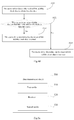
- An embodiment of the disclosure provides a data transmission method for the timing controller 100 in the application environment as shown in Fig. 1 . As shown in Fig. 2 , the method includes the following steps.
- preset link stability check data is sent to a source driver after clock calibration.
- the source driver may be any of the source drivers in the application environment as shown in Fig. 1 .
- step 102 feedback information sent by the source driver is received, wherein the feedback information is generated by the source driver when judging that the received link stability check data is correct.
- target data is sent to the source driver based on the feedback information.
- the timing controller can send link stability check data to the source driver, and when the link stability mode data received by the source driver is correct, which indicates that the data transmission state of the link is good, the source driver sends feedback information to the timing controller, such that the timing controller can send data to the source driver in a case in which the data transmission state of the link is good, the reliability and stability of data transmission is improved.
- An embodiment of the disclosure provides another data transmission method for any of the source drivers 200 in the application environment as shown in Fig. 1 .
- the method includes:
- the source driver receives link stability check data sent by the timing controller after clock calibration, and when the link stability mode data received by the source driver is correct, which indicates that the data transmission state of the link is good, the source driver sends feedback information to the timing controller, such that the timing controller can send data to the source driver in a case in which the data transmission state of the link is good, so the reliability and stability of data transmission is improved.
- An embodiment of the disclosure provides still another data transmission method for the application environment as shown in Fig. 1 .
- the method includes the following steps.
- a timing controller sends preset link stability check data to a source driver after clock calibration. Step 302 is to be performed.
- the source driver is any of the source drivers in the application environment as shown in Fig. 1 .
- the timing controller sends preset link stability check data to the source driver after the clock calibration.
- the timing controller and the source driver first perform a clock calibration operation, and then, the timing controller sends link stability check data to the source driver, to detect a data transmission state of a link between the timing controller and the source driver.
- the timing controller sends link stability check data to the source driver, which low power consumption wake-up state is a transitional state in which the timing controller reenters a data transmission state from a low power consumption state with no need for data transmission.
- the timing controller when the timing controller and the source driver do not need to transmit data, the timing controller enters a low power consumption state.
- the timing controller and the source driver need to transmit data again, the timing controller needs to enter a low power consumption wake-up state, to be recovered to a normal working state.
- the timing controller may send link stability check data to the source driver, to detect a data transmission state of a link between the timing controller and the source driver. This method may cause the timing controller to be recovered to the normal working state from the low power consumption wake-up state rapidly.
- the timing controller and the source driver when the timing controller and the source driver need to transmit data again, the timing controller and the source driver may be recovered to the normal working state without the need for a clock calibration operation.
- the step of sending link stability check data in the embodiment of the disclosure may also be performed when the timing controller is to enter other states, in addition to that this step may be performed when the timing controller is to enter the low power consumption wake-up state.
- the timing controller may send link stability check data to the source driver to detect the data transmission state of the link between the timing controller and the source driver.
- the timing controller may send an identity identification of the source driver to the source driver while the timing controller sends the preset link stability check data to the source driver.
- the source driver may detect whether the identity identification sent by the timing controller is the same as its own identity identification. When the identity identification sent by the timing controller is the same as its own identity identification, the source driver performs corresponding operations, with reference to steps 302 to 304 and step 306, etc.
- the link stability check data is obtained by encoding a multiple byte data code adopting an 8b/10b (namely, encoding 8-bit data into 10-bit data) encoding approach, and the multiple byte data code includes a start identification and data digits.
- the start identification is used for indicating start of data transmission
- the data digits carry verification data
- a scrambling identification is arranged in the data digits
- a position of the scrambling identification is used for indicating a port of the source driver and an initialization time point of a linear feedback shift register (LFSR for short) corresponding to the port
- LFSR linear feedback shift register
- the multiple byte data code may be obtained by adopting the 8b/10b encoding approach in the related art.
- encoding adopting the 8b/10b encoding approach it is to encode the verification data carried by the data digits in the multiple byte data code, and there is no need for encoding the special codes (e.g., the start identification, the scrambling identification, etc.).
- a set of consecutive 8-bit data is divided into two parts, 5B/6B (namely, encoding 5-bit data into 6-bit data) encoding is performed on the first 5 digits thereof, and 3B/4B (namely, encoding 3-bit data into 4-bit data) encoding is performed on the last 3 digits thereof.
- the boundary between every two sets of 10-bit data is blurry, and a transmission error easily appears.
- the byte to be encoded is the first byte of the verification data
- a tenth digit of data for indicating that the 9-bit data has not undergone an inversion operation is added behind the 9-bit data to obtain 10-bit data.
- the 8-bit data is encoded into 9-bit data first, then a tenth digit is added to obtain 10-bit data, a jumping edge is arranged between every two adjacent 10-bit data, and the tenth digit of data is used for indicating whether the 9-bit data has undergone an inversion operation, which can effectively ensure that the data to be transmitted is correctly restored at the receiving end, and the jumping edge may effectively reduce transmission errors.
- the multiple byte data code is a data code of 40 bytes, wherein the start identification is a K2 code of 4 bytes, the scrambling identification is a K3 code of 4 bytes, the verification data carried by the data digits includes 8 data units, and each of the data units includes a data code of 4 bytes.
- the start identification is a K2 code of 4 bytes
- the scrambling identification is a K3 code of 4 bytes
- the verification data carried by the data digits includes 8 data units
- each of the data units includes a data code of 4 bytes.
- the timing controller is coupled to a plurality of source drivers, each port of each of the source drivers may adopt a descrambling approach for received data, and this descrambling approach corresponds to a scrambling approach adopted by the timing controller for data to be sent. That is, a different port of each of the source drivers adopts a different descrambling approach. Nevertheless, for scrambling the target data, a port of each of the source drivers corresponds to an LFSR. The position of the scrambling identification in the data digits is used for indicating a port of the source driver and an initialization time point of an LFSR corresponding to the port.
- the source driver when the scrambling identification is a K3 code, after the source driver receives and decodes the link stability check data sent by the timing controller, the source driver will determine a time point for initializing an LFSR of a certain port according to the position of the K3 code in the data digits. If the time point at which the source driver initializes the LFSR for the port is different, the result after descrambling will be different.
- each of the 8 data units included in the verification data may include successively arranged 0xea, 0xeb, 0xec and 0xed, wherein data starting with 0x represents hexadecimal data, and in hexadecimal data, a represents decimal 10, b represents decimal 11, c represents decimal 12, d represents decimal 13, and e represents decimal 14.
- the source driver achieves the purpose of checking data according to the verification data. When what the source driver receives is correct verification data, it indicates that the data transmission state of the link is good.
- Fig. 4b shows a schematic diagram of a 40-byte data code sent to a port 01
- Fig. 4c shows a schematic diagram of a 40-byte data code sent to a port 02.
- the positions of the K3 codes in Fig. 4b and Fig. 4c are different. Assume that the initialization time point of the LFSR corresponding to the port 01 is t1, and the initialization time point of the LFSR corresponding to the port 01 is t2, and then t2 is different from t1.
- the step 301 may include: sending for a duration of 1 microsecond the link stability check data to the source driver n times, that is, the total duration in which the timing controller sends the link stability check data to the source driver n times being 1 microsecond, wherein n is greater than or equal to 5.
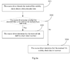
- step 302 the source driver judges whether the received link stability check data is correct. When the received link stability check data is correct, step 303 is to be performed; and when the received link stability check data is incorrect, step 306 is to be performed.
- the step 302 may include the following steps.
- the source driver decodes the received link stability check data to obtain decoded data.
- the decoded data includes the scrambling identification, and exemplarily, the decoded data includes a K3 code.
- the source driver judges whether the decoded data is the same as the multiple byte data code.
- step 3023 is to be performed; and when the decoded data is different from the multiple byte data code, step 3024 is to be performed.
- the source driver compares the decoded data with the multiple byte data code before the encoding, to judge whether the two are the same.
- the source driver determines that the received link stability check data is correct.
- the source driver judges whether the decoded data is the same as the multiple byte data code before the encoding, and when the decoded data is the same as the multiple byte data code, the source driver determines that the received link stability check data is correct.
- the method may further include: 1) The source driver determines the port of the source driver and the initialization time point of the LFSR corresponding to the port according to the position of the scrambling identification in the decoded data.
- the source driver determines the port of the source driver and the initialization time point of the LFSR corresponding to the port according to the position of the scrambling identification (e.g., the K3 code) in the decoded data.
- the source driver may determine a port of the source driver and the initialization time point of an LFSR corresponding to the port according to a preset correspondence relationship.
- the correspondence relationship is used for recording a correspondence relationship of a position of a scrambling identification in decoded data, a port of the source driver and an initialization time point of an LFSR.
- the correspondence relationship may be as shown in table 1.
- the source driver needs to initialize the LFSR corresponding to the port P01 for the port P01 at the time point T1.
- Table 1 Position of the scrambling identification in the decoded data Port of the source driver Initialization time point ofLFSR L1 P01 T1 L2 P02 T2 2) The source driver initializes the LFSR for the port according to the initialization time point.
- the source driver may initialize the LFSR according to the initialization time point, to facilitate scrambling and descrambling of subsequently transmitted data.
- the source driver determines that the received link stability check data is incorrect.
- the source driver determines that the received link stability check data is incorrect, which indicates that the data transmission state of the link between the timing controller and the source driver is poor, and at this point, it is unsuitable to transmit display data, configuration data, etc.
- Step 303 when the received link stability check data is correct, the source driver generates feedback information. Step 304 is to be performed.
- the source driver may generate feedback information, and send the feedback information to the timing controller, so as to inform the timing controller that the data transmission state of the current link is good and adapted for transmitting display data, configuration data, etc.
- Step 304 the source driver sends the feedback information to the timing controller. Step 305 is to be performed.
- the source driver sends the generated feedback information to the timing controller and informs the timing controller that the data transmission state of the current link is good, and then the timing controller sends target data to the source driver.
- the timing controller sends target data to the source driver based on the feedback information.
- the target data is display data or configuration data.
- the source driver repeatedly performs a phase calibration operation when the received link stability check data is incorrect, until correct link stability check data is received.
- the source driver may repeatedly perform a phase calibration operation to implement phase shift, until correct link stability check data is received, and in turn the data transmission state of the link is made good and more suitable for transmitting the target data. Then, the steps 303 to 305 are performed again, to complete transmission of the target data.
- the timing controller sends the target data to the source driver only when the source driver has received correct link stability check data, which improves the reliability and stability of data transmission.
- the source driver may stop receiving the link stability check data.
- the source driver may stop receiving the link stability check data.
- the timing controller After generating the link stability check data containing the interruption identification, the timing controller sends the link stability check data to the source driver, such that the source driver stops receiving link stability check data based on the interruption identification. 3. The source driver stops receiving link stability check data.
- the source driver When the source driver receives the link stability check data containing the interruption identification (e.g., K1 code or K4 code) sent by the timing controller, the source driver stops receiving link stability check data.
- the interruption identification e.g., K1 code or K4 code
- a data transmission method provided by an embodiment of the disclosure is adapted for the P2P interface protocol, this method is adapted for any product or component with the display function adopting the P2P interface protocol, and this method may cause the link between a sending end and a receiving end of a P2P interface to be more stable.
- the timing controller can send link stability check data to the source driver, and when the link stability mode data received by the source driver is correct, which indicates that the data transmission state of the link is good, the source driver sends feedback information to the timing controller, such that the timing controller can only send data to the source driver in a case in which the data transmission state of the link is good.
- This method causes the link to be more stable, and can cause the timing controller to be rapidly recovered to a normal working state from a low power consumption wake-up state. This method improves the reliability and stability of data transmission.
- An embodiment of the disclosure provides a data transmission circuit for the timing controller 100 in the application environment as shown in Fig. 1 , as shown in Fig. 5a , the data transmission circuit 500 including:
- the timing controller can send link stability check data to the source driver, and when the link stability mode data received by the source driver is correct, which indicates that the data transmission state of the link is good, the source driver sends feedback information to the timing controller, such that the timing controller can send data to the source driver in a case in which the data transmission state of the link is good, the reliability and stability of data transmission is improved.
- the first sender 510 is specifically used for: sending the link stability check data to the source driver when the timing controller is to enter a low power consumption wake-up state, wherein the low power consumption wake-up state is a transitional state in which the timing controller reenters a data transmission state from a low power consumption state with no need for data transmission.
- the link stability check data is obtained by encoding a multiple byte data code adopting an 8b/10b encoding approach, the multiple byte data code includes a start identification and data digits.
- the start identification is used for indicating start of data transmission
- the data digits carry verification data
- a scrambling identification is arranged in the data digits
- a position of the scrambling identification is used for indicating a port of the source driver and an initialization time point of an LFSR corresponding to the port
- the LFSR is used for scrambling of the target data.
- the multiple byte data code is a data code of 40 bytes
- the start identification is a K2 code of 4 bytes
- the scrambling identification is a K3 code of 4 bytes
- the verification data carried by the data digits includes 8 data units, each of the data units includes a data code of 4 bytes, and there exists at least a data code of 4 bytes between the start identification and the scrambling identification.
- the first sender 510 is specifically used for: sending for a duration of 1 microsecond the link stability check data to the source driver n times, n being greater than or equal to 5.
- the data transmission circuit 500 may further include: a generator 540 for generating link stability check data containing an interruption identification when a transmission interruption instruction is received; and a third sender 550 for sending the link stability check data containing the interruption identification to the source driver, to cause the source driver to stop receiving link stability check data.
- the interruption identification is a K1 code or a K4 code.
- the target data is display data or configuration data.
- the timing controller can send link stability check data to the source driver, and when the link stability mode data received by the source driver is correct, which indicates that the data transmission state of the link is good, the source driver sends feedback information to the timing controller, such that the timing controller can send data to the source driver in a case in which the data transmission state of the link is good, the reliability and stability of data transmission is improved.
- An embodiment of the disclosure provides another data transmission circuit for any of the source drivers 200 in the application environment as shown in Fig. 1 , as shown in Fig. 6a , the data transmission circuit 600 including:
- the source driver receives preset link stability check data sent by the timing controller after clock calibration, and when the link stability mode data received by the source driver is correct, which indicates that the data transmission state of the link is good, the source driver sends feedback information to the timing controller, such that the timing controller can send data to the source driver in a case in which the data transmission state of the link is good, so the reliability and stability of data transmission is improved.
- the link stability check data is obtained by encoding a multiple byte data code adopting an 8b/10b encoding approach
- the multiple byte data code includes a start identification and data digits
- the start identification is used for indicating start of data transmission
- the data digits carry verification data
- a scrambling identification is arranged in the data digits
- a position of the scrambling identification is used for indicating a port of the source driver and an initialization time point of an LFSR corresponding to the port
- the LFSR is used for scrambling of the target data.
- the multiple byte data code is a data code of 40 bytes
- the start identification is a K2 code of 4 bytes
- the scrambling identification is a K3 code of 4 bytes
- the verification data carried by the data digits includes 8 data units, each of the data units includes a data code of 4 bytes, and there exists at least a data code of 4 bytes between the start identification and the scrambling identification.
- the receiver 610 is specifically used for: receiving for a duration of 1 microsecond the link stability check data sent n times by the timing controller, n being greater than or equal to 5.
- the data transmission circuit 600 may further include: a first processor 640 for stopping receiving link stability check data when link stability check data containing an interruption identification sent by the timing controller is received, the link stability check data containing an interruption identification being generated by the timing controller when receiving a transmission interruption instruction.
- the data transmission circuit 600 may further include: a second processor 650 for repeatedly performing a phase calibration operation when the received link stability check data is incorrect, until correct link stability check data is received.
- the judger 620 is specifically used for: decoding the received link stability check data to obtain decoded data, wherein the decoded data includes the scrambling identification; judging whether the decoded data is the same as the multiple byte data code; determining that the received link stability check data is correct when the decoded data is the same as the multiple byte data code; and determining that the received link stability check data is incorrect when the decoded data is different from the multiple byte data code.
- the judger 620 is further used for: determining the port of the source driver and the initialization time point of the LFSR corresponding to the port according to the position of the scrambling identification in the decoded data; and initializing the LFSR for the port according to the initialization time point.
- the source driver receives preset link stability check data sent by the timing controller after clock calibration, and when the link stability mode data received by the source driver is correct, which indicates that the data transmission state of the link is good, the source driver sends feedback information to the timing controller, such that the timing controller can send data to the source driver in a case in which the data transmission state of the link is good, so the reliability and stability of data transmission is improved.
- An embodiment of the disclosure further provides a display device including a timing controller and a source driver.
- the timing controller includes a data transmission circuit as shown in Fig. 5a or Fig. 5b
- the source driver includes a data transmission circuit as shown in the Fig. 6a or Fig. 6b .
- the display device may be any product or component with the display function, such as a liquid crystal panel, an electronic paper, an organic light emitting diode (OLED for short) panel, a mobile phone, a tablet computer, a television, a display, a notebook computer, a digital photo frame, a navigator, etc.
- a liquid crystal panel an electronic paper
- OLED organic light emitting diode
- An embodiment of the disclosure further provides a computer readable storage medium storing an instruction therein, which, when running on a computer, causes the computer to perform a data transmission method as shown in Fig. 2 or Fig. 4a .
- An embodiment of the disclosure further provides a computer readable storage medium storing an instruction therein, which, when running on a computer, causes the computer to perform a data transmission method as shown in Fig. 3 or Fig. 4a .
Landscapes
- Engineering & Computer Science (AREA)
- Physics & Mathematics (AREA)
- Computer Hardware Design (AREA)
- General Physics & Mathematics (AREA)
- Theoretical Computer Science (AREA)
- Chemical & Material Sciences (AREA)
- Crystallography & Structural Chemistry (AREA)
- Control Of Indicators Other Than Cathode Ray Tubes (AREA)
- Communication Control (AREA)
Abstract
Description
- This application claims the priority of the Chinese patent application No.
201710433373.10 filed on June 9, 2017 - This application relates to the field of display manufacturing, and in particular, to a data transmission method, a data transmission circuit, a display device and a storage medium.
- A point-to-point (P2P for short) interface is a high speed serial interface applied between a timing controller (T-CON for short) and a source driver (SD for short) inside a display panel of a liquid crystal display. Transmission of data such as display data and configuration data, etc. may be accomplished through the P2P interface.
- In the related art, there is a data transmission method in which the timing controller and the source driver perform a clock calibration operation first, and then the timing controller sends data needing to be transmitted to the source driver.
- Embodiments of the disclosure provide a data transmission method, a data transmission circuit, a display device and a storage medium. The technical solutions are as follows.
- In a first aspect, there is provided a data transmission method for a timing controller, the method including: sending preset link stability check data to a source driver after clock calibration; receiving feedback information sent by the source driver, wherein the feedback information is generated by the source driver when judging that the received link stability check data is correct; and sending target data to the source driver based on the feedback information.
- Exemplarily, the sending preset link stability check data to a source driver includes: sending the link stability check data to the source driver when the timing controller is to enter a low power consumption wake-up state, wherein the low power consumption wake-up state is a transitional state in which the timing controller reenters a data transmission state from a low power consumption state with no need for data transmission.
- Exemplarily, the link stability check data is obtained by encoding a multiple byte data code adopting an 8b/10b encoding approach, the multiple byte data code includes a start identification and data digits, the start identification is used for indicating start of data transmission, the data digits carry verification data, a scrambling identification is arranged in the data digits, a position of the scrambling identification is used for indicating a port of the source driver and an initialization time point of a linear feedback shift register LFSR corresponding to the port, and the LFSR is used for scrambling of the target data.
- Exemplarily, the multiple byte data code is a data code of 40 bytes, the start identification is a K2 code of 4 bytes, the scrambling identification is a K3 code of 4 bytes, the verification data carried by the data digits includes 8 data units, each of the data units includes a data code of 4 bytes, and there exists at least a data code of 4 bytes between the start identification and the scrambling identification.
- Exemplarily, the sending preset link stability check data to a source driver includes: sending for a duration of 1 microsecond the link stability check data to the source driver n times, n being greater than or equal to 5.
- Exemplarily, after the sending preset link stability check data to a source driver, the method further includes: generating link stability check data containing an interruption identification in response to receiving a transmission interruption instruction; and sending the link stability check data containing the interruption identification to the source driver, to instruct the source driver to stop receiving link stability check data.
- Exemplarily, the interruption identification is a K1 code or a K4 code.
- Exemplarily, the target data is display data or configuration data.
- In a second aspect, there is provided a data transmission method for a source driver, the method including:
receiving preset link stability check data sent by a timing controller after clock calibration; judging whether the received link stability check data is correct; and generating feedback information in response to the received link stability check data being correct, and sending the feedback information to the timing controller, such that the timing controller sends target data to the source driver based on the feedback information. - Exemplarily, the link stability check data is obtained by encoding a multiple byte data code adopting an 8b/10b encoding approach, the multiple byte data code includes a start identification and data digits, the start identification is used for indicating start of data transmission, the data digits carry verification data, a scrambling identification is arranged in the data digits, a position of the scrambling identification is used for indicating a port of the source driver and an initialization time point of a linear feedback shift register LFSR corresponding to the port, and the LFSR is used for scrambling of the target data.
- Exemplarily, the multiple byte data code is a data code of 40 bytes, the start identification is a K2 code of 4 bytes, the scrambling identification is a K3 code of 4 bytes, the verification data carried by the data digits includes 8 data units, each of the data units includes a data code of 4 bytes, and there exists at least a data code of 4 bytes between the start identification and the scrambling identification.
- Exemplarily, the receiving preset link stability check data sent by a timing controller after clock calibration includes: receiving for a duration of 1 microsecond the link stability check data sent n times by the timing controller, n being greater than or equal to 5.
- Exemplarily, after the receiving preset link stability check data sent by a timing controller after clock calibration, the method further includes: stopping receiving link stability check data in response to receiving link stability check data containing an interruption identification sent by the timing controller, the link stability check data containing an interruption identification being generated by the timing controller when receiving a transmission interruption instruction.
- Exemplarily, after the judging whether the received link stability check data is correct, the method further includes: repeatedly performing a phase calibration operation in response to the received link stability check data being incorrect, until correct link stability check data is received.
- Exemplarily, the judging whether the received link stability check data is correct includes: decoding the received link stability check data to obtain decoded data, wherein the decoded data includes the scrambling identification; judging whether the decoded data is the same as the multiple byte data code; determining that the received link stability check data is correct in response to the decoded data being the same as the multiple byte data code; and determining that the received link stability check data is incorrect in response to the decoded data being different from the multiple byte data code.
- Exemplarily, after the determining that the received link stability check data is correct, the method further includes: determining the port of the source driver and the initialization time point of the linear feedback shift register LFSR corresponding to the port according to the position of the scrambling identification in the decoded data; and initializing the LFSR for the port according to the initialization time point.
- In a third aspect, there is provided a data transmission circuit for a timing controller, the data transmission circuit including: a first sender for sending preset link stability check data to a source driver after clock calibration; a receiver for receiving feedback information sent by the source driver, wherein the feedback information is generated by the source driver when judging that the received link stability check data is correct; and a second sender for sending target data to the source driver based on the feedback information.
- Exemplarily, the first sender is specifically used for: sending the link stability check data to the source driver when the timing controller is to enter a low power consumption wake-up state, wherein the low power consumption wake-up state is a transitional state in which the timing controller reenters a data transmission state from a low power consumption state with no need for data transmission.
- Exemplarily, the link stability check data is obtained by encoding a multiple byte data code adopting an 8b/10b encoding approach, the multiple byte data code includes a start identification and data digits,
the start identification is used for indicating start of data transmission, the data digits carry verification data, a scrambling identification is arranged in the data digits, a position of the scrambling identification is used for indicating a port of the source driver and an initialization time point of a linear feedback shift register LFSR corresponding to the port, and the LFSR is used for scrambling of the target data. - Exemplarily, the multiple byte data code is a data code of 40 bytes, the start identification is a K2 code of 4 bytes, the scrambling identification is a K3 code of 4 bytes, the verification data carried by the data digits includes 8 data units, each of the data units includes a data code of 4 bytes, and there exists at least a data code of 4 bytes between the start identification and the scrambling identification.
- Exemplarily, the first sender is specifically used for: sending for a duration of 1 microsecond the link stability check data to the source driver n times, n being greater than or equal to 5.
- Exemplarily, the data transmission circuit further includes: a generator for generating link stability check data containing an interruption identification when a transmission interruption instruction is received; and a third sender for sending the link stability check data containing the interruption identification to the source driver, to instruct the source driver to stop receiving link stability check data.
- Exemplarily, the interruption identification is a K1 code or a K4 code.
- Exemplarily, the target data is display data or configuration data.
- In a fourth aspect, there is provided a data transmission circuit for a source driver, the data transmission circuit including: a receiver for receiving preset link stability check data sent by a timing controller after clock calibration; a judger for judging whether the received link stability check data is correct; and a generator for generating feedback information when the received link stability check data is correct, and sending the feedback information to the timing controller, such that the timing controller sends target data to the source driver based on the feedback information.
- Exemplarily, the data transmission circuit further includes: a first processor for stopping receiving link stability check data when link stability check data containing an interruption identification sent by the timing controller is received, the link stability check data containing an interruption identification being generated by the timing controller when receiving a transmission interruption instruction.
- Exemplarily, the data transmission circuit further includes: a second processor for repeatedly performing a phase calibration operation when the received link stability check data is incorrect, until correct link stability check data is received.
- Exemplarily, the judger is specifically used for: decoding the received link stability check data to obtain decoded data, wherein the decoded data includes the scrambling identification; judging whether the decoded data is the same as the multiple byte data code; determining that the received link stability check data is correct in response to the decoded data being the same as the multiple byte data code; and determining that the received link stability check data is incorrect in response to the decoded data being different from the multiple byte data code; wherein the link stability check data is obtained by encoding a multiple byte data code adopting an 8b/10b encoding approach, the multiple byte data code includes a start identification and data digits, the start identification is used for indicating start of data transmission, the data digits carry verification data, the scrambling identification is arranged in the data digits, a position of the scrambling identification is used for indicating a port of the source driver and an initialization time point of a linear feedback shift register LFSR corresponding to the port, and the LFSR is used for scrambling of the target data.
- Exemplarily, the judger is further used for: determining the port of the source driver and the initialization time point of the linear feedback shift register LFSR corresponding to the port according to the position of the scrambling identification in the decoded data; and initializing the LFSR for the port according to the initialization time point.
- In a fifth aspect, there is provided a display device including a timing controller and a source driver, the timing controller includes a data transmission circuit as described in the third aspect, and the source driver includes a data transmission circuit as described in the fourth aspect.
- In a sixth aspect, there is provided a computer readable storage medium storing an instruction therein which, when running on a computer, causes the computer to perform any of the described data transmission methods in the first aspect.
- In a seventh aspect, there is provided a computer readable storage medium storing an instruction therein which, when running on a computer, causes the computer to perform any of the described data transmission methods in the second aspect.
- In order to more clearly illustrate the technical solutions in the embodiments of the disclosure, the appended drawings needing to be used in the description of the embodiments will be introduced briefly in the following. Obviously, the drawings in the following description are only some embodiments of this application, and for the person having ordinary skills in the art, other drawings may also be obtained according to these drawings under the premise of not paying out undue experimentation.
-
Fig. 1 is a schematic diagram of an application environment of a data transmission method provided by an embodiment of the disclosure. -
Fig. 2 is a flow chart of a data transmission method provided by an embodiment of the disclosure. -
Fig. 3 is a flow chart of another data transmission method provided by an embodiment of the disclosure. -
Fig. 4a is a flow chart of still another data transmission method provided by an embodiment of the disclosure. -
Fig. 4b is a schematic diagram of a 40-byte data code sent to a port provided by an embodiment of the disclosure. -
Fig. 4c is a schematic diagram of a 40-byte data code sent to another port provided by an embodiment of the disclosure. -
Fig. 4d is a flow chart of judging whether link stability check data is correct provided by an embodiment of the disclosure. -
Fig. 5a is a structure diagram of a data transmission circuit provided by an embodiment of the disclosure. -
Fig. 5b is a structure diagram of another data transmission circuit provided by an embodiment of the disclosure. -
Fig. 6a is a structure diagram of still another data transmission circuit provided by an embodiment of the disclosure. -
Fig. 6b is a structure diagram of yet still another data transmission circuit provided by an embodiment of the disclosure. - To make the objects, technical solutions and advantages of this application clearer, in the following, the implementations of this application will be further described in detail in conjunction with the drawings.
-
Fig. 1 shows a schematic diagram of an application environment of a data transmission method provided by an embodiment of the disclosure. As shown inFig. 1 , the data transmission method is applied in a display device, which includes atiming controller 100 and a plurality ofsource drivers 200. A plurality of high speed signal lines H of thetiming controller 100 are coupled to the plurality ofsource drivers 200 in a one to one correspondence. Thetiming controller 100 is also coupled to a low speed signal line L, and the plurality ofsource drivers 200 are connected in parallel and coupled to the low speed signal line L. A P2P interface is a high speed serial interface between thetiming controller 100 and asource driver 200, and transmission of data such as display data, configuration data, etc. may be accomplished by the P2P interface. Therein, clock calibration is an important part of the P2P interface technology. In the related art, thetiming controller 100 directly sends data after the clock calibration operation is completed, thesource driver 200 also directly receives data after the clock calibration operation is completed, a data transmission state of a link between the timing controller and the source driver (also called a P2P interface link) is not detected in advance in the whole procedure, and in a case in which the data transmission state of the link is poor, thetiming controller 100 will also send data to thesource driver 200, and finally, thesource driver 200 is apt to receive erroneous data. - Yet in embodiments of the disclosure, the
timing controller 100 and thesource driver 200 will detect the data transmission state of the link, and when the data transmission state of the link is good, thetiming controller 100 then sends data such as display data and configuration data, etc. to thesource driver 200. - An embodiment of the disclosure provides a data transmission method for the
timing controller 100 in the application environment as shown inFig. 1 . As shown inFig. 2 , the method includes the following steps. - At
step 101, preset link stability check data is sent to a source driver after clock calibration. - The source driver may be any of the source drivers in the application environment as shown in
Fig. 1 . - At
step 102, feedback information sent by the source driver is received, wherein the feedback information is generated by the source driver when judging that the received link stability check data is correct. - At
step 103, target data is sent to the source driver based on the feedback information. - From the above, in the data transmission method provided by the embodiment of the disclosure, since the timing controller can send link stability check data to the source driver, and when the link stability mode data received by the source driver is correct, which indicates that the data transmission state of the link is good, the source driver sends feedback information to the timing controller, such that the timing controller can send data to the source driver in a case in which the data transmission state of the link is good, the reliability and stability of data transmission is improved.
- An embodiment of the disclosure provides another data transmission method for any of the
source drivers 200 in the application environment as shown inFig. 1 . As shown inFig. 3 , the method includes: -
step 201, receiving preset link stability check data sent by a timing controller after clock calibration; -
step 202, judging whether the received link stability check data is correct; and -
step 203, generating feedback information when the received link stability check data is correct, and sending the feedback information to the timing controller, such that the timing controller sends target data to the source driver based on the feedback information. - From the above, in the data transmission method provided by the embodiment of the disclosure, the source driver receives link stability check data sent by the timing controller after clock calibration, and when the link stability mode data received by the source driver is correct, which indicates that the data transmission state of the link is good, the source driver sends feedback information to the timing controller, such that the timing controller can send data to the source driver in a case in which the data transmission state of the link is good, so the reliability and stability of data transmission is improved.
- An embodiment of the disclosure provides still another data transmission method for the application environment as shown in
Fig. 1 . As shown inFig. 4a , the method includes the following steps. - At
step 301, a timing controller sends preset link stability check data to a source driver after clock calibration. Step 302 is to be performed. - The source driver is any of the source drivers in the application environment as shown in
Fig. 1 . - On one hand, the timing controller sends preset link stability check data to the source driver after the clock calibration.
- In the embodiment of the disclosure, the timing controller and the source driver first perform a clock calibration operation, and then, the timing controller sends link stability check data to the source driver, to detect a data transmission state of a link between the timing controller and the source driver.
- On the other hand, after the clock calibration and when the timing controller is to enter a low power consumption wake-up state, the timing controller sends link stability check data to the source driver, which low power consumption wake-up state is a transitional state in which the timing controller reenters a data transmission state from a low power consumption state with no need for data transmission.
- In the embodiment of the disclosure, when the timing controller and the source driver do not need to transmit data, the timing controller enters a low power consumption state. When the timing controller and the source driver need to transmit data again, the timing controller needs to enter a low power consumption wake-up state, to be recovered to a normal working state. When the timing controller is to enter the low power consumption wake-up state, the timing controller may send link stability check data to the source driver, to detect a data transmission state of a link between the timing controller and the source driver. This method may cause the timing controller to be recovered to the normal working state from the low power consumption wake-up state rapidly.
- In the embodiment of the disclosure, when the timing controller and the source driver need to transmit data again, the timing controller and the source driver may be recovered to the normal working state without the need for a clock calibration operation.
- It needs to be added that, the step of sending link stability check data in the embodiment of the disclosure may also be performed when the timing controller is to enter other states, in addition to that this step may be performed when the timing controller is to enter the low power consumption wake-up state. As long as it is to return to the normal working state, the timing controller may send link stability check data to the source driver to detect the data transmission state of the link between the timing controller and the source driver.
- In an embodiment of the disclosure, the timing controller may send an identity identification of the source driver to the source driver while the timing controller sends the preset link stability check data to the source driver. The source driver may detect whether the identity identification sent by the timing controller is the same as its own identity identification. When the identity identification sent by the timing controller is the same as its own identity identification, the source driver performs corresponding operations, with reference to steps 302 to 304 and step 306, etc.
- Exemplarily, the link stability check data is obtained by encoding a multiple byte data code adopting an 8b/10b (namely, encoding 8-bit data into 10-bit data) encoding approach, and the multiple byte data code includes a start identification and data digits.
- Therein, the start identification is used for indicating start of data transmission, the data digits carry verification data, a scrambling identification is arranged in the data digits, a position of the scrambling identification is used for indicating a port of the source driver and an initialization time point of a linear feedback shift register (LFSR for short) corresponding to the port, and the LFSR is used for scrambling of target data. Using some special codes such as the start identification, the scrambling identification, etc., it may be possible to assist a receiving end in restoration, and find out a data code transmission error early, and thereby inhibiting errors from continuing to occur.
- Therein, the multiple byte data code may be obtained by adopting the 8b/10b encoding approach in the related art. When encoding adopting the 8b/10b encoding approach, it is to encode the verification data carried by the data digits in the multiple byte data code, and there is no need for encoding the special codes (e.g., the start identification, the scrambling identification, etc.).
- When encoding adopting the 8b/10b encoding approach, it may be such that the numbers of "0s" and "1s" keep basically consistent, and consecutive "0s" and "1s" do not exceed 5 digits, that is, one digit of "0" must be inserted behind every 5 consecutive "Is", and one digit of "1" must be inserted behind every 5 consecutive "0s", thereby guaranteeing signal DC (direct current) balance.
- When encoding the verification data adopting the 8b/10b encoding approach in the related art, in particular, a set of consecutive 8-bit data is divided into two parts, 5B/6B (namely, encoding 5-bit data into 6-bit data) encoding is performed on the first 5 digits thereof, and 3B/4B (namely, encoding 3-bit data into 4-bit data) encoding is performed on the last 3 digits thereof.
- However, in the data obtained by encoding adopting the 8b/10b encoding approach in the related art, the boundary between every two sets of 10-bit data is blurry, and a transmission error easily appears. Hence, to ensure that data to be transmitted can be correctly restored at a receiving end, in an embodiment of the disclosure, when encoding the verification data, it may be possible to first encode 8-bit data corresponding to a byte to be encoded of the verification data into 9-bit data, and when the byte to be encoded is not the first byte of the verification data, detect the first digit of data of the 9-bit data and a previous digit of data adjacent to the first digit of data; when the numerical value of the first digit of data is the same as that of the previous digit of data, invert the 9-bit data and then add a tenth digit of data for indicating that the 9-bit data has undergone an inversion operation behind the 9-bit data to obtain 10-bit data; and when the numerical value of the first digit of data is different from that of the previous digit of data, add a tenth digit of data for indicating that the 9-bit data has not undergone an inversion operation behind the 9-bit data to obtain 10-bit data; wherein the 10-bit data is binary data. When the byte to be encoded is the first byte of the verification data, a tenth digit of data for indicating that the 9-bit data has not undergone an inversion operation is added behind the 9-bit data to obtain 10-bit data. In the encoding procedure, the 8-bit data is encoded into 9-bit data first, then a tenth digit is added to obtain 10-bit data, a jumping edge is arranged between every two adjacent 10-bit data, and the tenth digit of data is used for indicating whether the 9-bit data has undergone an inversion operation, which can effectively ensure that the data to be transmitted is correctly restored at the receiving end, and the jumping edge may effectively reduce transmission errors.
- Exemplarily, the multiple byte data code is a data code of 40 bytes, wherein the start identification is a K2 code of 4 bytes, the scrambling identification is a K3 code of 4 bytes, the verification data carried by the data digits includes 8 data units, and each of the data units includes a data code of 4 bytes. To accomplish data check for at least one time, there exists at least a data code of 4 bytes between the start identification and the scrambling identification.
- In an embodiment of the disclosure, the timing controller is coupled to a plurality of source drivers, each port of each of the source drivers may adopt a descrambling approach for received data, and this descrambling approach corresponds to a scrambling approach adopted by the timing controller for data to be sent. That is, a different port of each of the source drivers adopts a different descrambling approach. Nevertheless, for scrambling the target data, a port of each of the source drivers corresponds to an LFSR. The position of the scrambling identification in the data digits is used for indicating a port of the source driver and an initialization time point of an LFSR corresponding to the port. Exemplarily, when the scrambling identification is a K3 code, after the source driver receives and decodes the link stability check data sent by the timing controller, the source driver will determine a time point for initializing an LFSR of a certain port according to the position of the K3 code in the data digits. If the time point at which the source driver initializes the LFSR for the port is different, the result after descrambling will be different.
- Exemplarily, each of the 8 data units included in the verification data may include successively arranged 0xea, 0xeb, 0xec and 0xed, wherein data starting with 0x represents hexadecimal data, and in hexadecimal data, a represents decimal 10, b represents decimal 11, c represents decimal 12, d represents decimal 13, and e represents decimal 14. The source driver achieves the purpose of checking data according to the verification data. When what the source driver receives is correct verification data, it indicates that the data transmission state of the link is good.
- Exemplarily,
Fig. 4b shows a schematic diagram of a 40-byte data code sent to aport 01, andFig. 4c shows a schematic diagram of a 40-byte data code sent to aport 02. The positions of the K3 codes inFig. 4b and Fig. 4c are different. Assume that the initialization time point of the LFSR corresponding to theport 01 is t1, and the initialization time point of the LFSR corresponding to theport 01 is t2, and then t2 is different from t1. - Further, for performing multiple time check and initializing the LFSR to reduce the probability of a subsequent error, the
step 301 may include: sending for a duration of 1 microsecond the link stability check data to the source driver n times, that is, the total duration in which the timing controller sends the link stability check data to the source driver n times being 1 microsecond, wherein n is greater than or equal to 5. - At step 302, the source driver judges whether the received link stability check data is correct. When the received link stability check data is correct, step 303 is to be performed; and when the received link stability check data is incorrect,
step 306 is to be performed. - In particular, as shown in
Fig. 4d , the step 302 may include the following steps. - At
step 3021, the source driver decodes the received link stability check data to obtain decoded data. - The decoded data includes the scrambling identification, and exemplarily, the decoded data includes a K3 code.
- At
step 3022, the source driver judges whether the decoded data is the same as the multiple byte data code. When the decoded data is the same as the multiple byte data code,step 3023 is to be performed; and when the decoded data is different from the multiple byte data code,step 3024 is to be performed. - The source driver compares the decoded data with the multiple byte data code before the encoding, to judge whether the two are the same.
- At the
step 3023, the source driver determines that the received link stability check data is correct. - Based on the
step 3022, the source driver judges whether the decoded data is the same as the multiple byte data code before the encoding, and when the decoded data is the same as the multiple byte data code, the source driver determines that the received link stability check data is correct. - Further, after the
step 3023, the method may further include:
1) The source driver determines the port of the source driver and the initialization time point of the LFSR corresponding to the port according to the position of the scrambling identification in the decoded data.
When the decoded data is the same as the multiple byte data code, the source driver determines the port of the source driver and the initialization time point of the LFSR corresponding to the port according to the position of the scrambling identification (e.g., the K3 code) in the decoded data. As described above, if the time point at which the source driver initializes the LFSR for the port is different, the result after descrambling will be different, and therefore, the source driver needs to obtain the initialization time point of the LFSR corresponding to the port according to the position of the scrambling identification in the decoded data.
Exemplarily, the source driver may determine a port of the source driver and the initialization time point of an LFSR corresponding to the port according to a preset correspondence relationship. The correspondence relationship is used for recording a correspondence relationship of a position of a scrambling identification in decoded data, a port of the source driver and an initialization time point of an LFSR. Exemplarily, the correspondence relationship may be as shown in table 1. For example, when the position of the scrambling identification in the decoded data is L1, it may be determined that the port of the source driver is PO1, and the initialization time point of the LFSR corresponding to the port P01 is T1. That is, the source driver needs to initialize the LFSR corresponding to the port P01 for the port P01 at the time point T1.Table 1 Position of the scrambling identification in the decoded data Port of the source driver Initialization time point ofLFSR L1 P01 T1 L2 P02 T2
2) The source driver initializes the LFSR for the port according to the initialization time point. - After obtaining the initialization time point of the LFSR corresponding to the port, the source driver may initialize the LFSR according to the initialization time point, to facilitate scrambling and descrambling of subsequently transmitted data.
- At the
step 3024, the source driver determines that the received link stability check data is incorrect. - When the decoded data is different from the multiple byte data code before the encoding, the source driver determines that the received link stability check data is incorrect, which indicates that the data transmission state of the link between the timing controller and the source driver is poor, and at this point, it is unsuitable to transmit display data, configuration data, etc.
- At the step 303, when the received link stability check data is correct, the source driver generates feedback information. Step 304 is to be performed.
- When the link stability check data received by the source driver is correct, the source driver may generate feedback information, and send the feedback information to the timing controller, so as to inform the timing controller that the data transmission state of the current link is good and adapted for transmitting display data, configuration data, etc.
- At the
step 304, the source driver sends the feedback information to the timing controller. Step 305 is to be performed. - The source driver sends the generated feedback information to the timing controller and informs the timing controller that the data transmission state of the current link is good, and then the timing controller sends target data to the source driver.
- At the step 305, the timing controller sends target data to the source driver based on the feedback information.
- Exemplarily, the target data is display data or configuration data.
- At the
step 306, the source driver repeatedly performs a phase calibration operation when the received link stability check data is incorrect, until correct link stability check data is received. - Exemplarily, when the link stability check data received by the source driver is incorrect, the source driver may repeatedly perform a phase calibration operation to implement phase shift, until correct link stability check data is received, and in turn the data transmission state of the link is made good and more suitable for transmitting the target data. Then, the steps 303 to 305 are performed again, to complete transmission of the target data.
- In an embodiment of the disclosure, the timing controller sends the target data to the source driver only when the source driver has received correct link stability check data, which improves the reliability and stability of data transmission.
- Further, in an embodiment of the disclosure, in the procedure of transmitting the link stability check data, when a user needs to interrupt transmission of the link stability check data, or when an anomaly occurs in the display device, the source driver may stop receiving the link stability check data. In particular, there may be included the following steps.
- 1. The timing controller generates link stability check data containing an interruption identification when receiving a transmission interruption instruction.
The transmission interruption instruction may be triggered by the user, or may also be triggered when an anomaly occurs to the display device. When the user needs to interrupt transmission of link stability check data, the user may trigger a transmission interruption instruction, and the timing controller generates link stability check data containing an interruption identification when receiving the transmission interruption instruction. When an anomaly occurs to the display device, a transmission interruption instruction will also be triggered, and the timing controller will also generate link stability check data containing an interruption identification when receiving the transmission interruption instruction, so that the source driver stops receiving link stability check data based on the interruption identification.
Exemplarily, the interruption identification is a K1 code or a K4 code. That is, when the source driver receives the K1 code or K4 code, it will stop receiving link stability check data. - 2. The timing controller sends the link stability check data containing the interruption identification to the source driver.
- After generating the link stability check data containing the interruption identification, the timing controller sends the link stability check data to the source driver, such that the source driver stops receiving link stability check data based on the interruption identification. 3. The source driver stops receiving link stability check data.
- When the source driver receives the link stability check data containing the interruption identification (e.g., K1 code or K4 code) sent by the timing controller, the source driver stops receiving link stability check data.
- It needs to be added that, a data transmission method provided by an embodiment of the disclosure is adapted for the P2P interface protocol, this method is adapted for any product or component with the display function adopting the P2P interface protocol, and this method may cause the link between a sending end and a receiving end of a P2P interface to be more stable.
- From the above, in the data transmission method provided by the embodiments of the disclosure, the timing controller can send link stability check data to the source driver, and when the link stability mode data received by the source driver is correct, which indicates that the data transmission state of the link is good, the source driver sends feedback information to the timing controller, such that the timing controller can only send data to the source driver in a case in which the data transmission state of the link is good. This method causes the link to be more stable, and can cause the timing controller to be rapidly recovered to a normal working state from a low power consumption wake-up state. This method improves the reliability and stability of data transmission.
- An embodiment of the disclosure provides a data transmission circuit for the
timing controller 100 in the application environment as shown inFig. 1 , as shown inFig. 5a , thedata transmission circuit 500 including: - a
first sender 510 for sending preset link stability check data to a source driver after clock calibration; - a
receiver 520 for receiving feedback information sent by the source driver, wherein the feedback information is generated by the source driver when judging that the received link stability check data is correct; and - a
second sender 530 for sending target data to the source driver based on the feedback information. - From the above, in the data transmission circuit provided by the embodiment of the disclosure, since the timing controller can send link stability check data to the source driver, and when the link stability mode data received by the source driver is correct, which indicates that the data transmission state of the link is good, the source driver sends feedback information to the timing controller, such that the timing controller can send data to the source driver in a case in which the data transmission state of the link is good, the reliability and stability of data transmission is improved.
- Exemplarily, the
first sender 510 is specifically used for:
sending the link stability check data to the source driver when the timing controller is to enter a low power consumption wake-up state, wherein the low power consumption wake-up state is a transitional state in which the timing controller reenters a data transmission state from a low power consumption state with no need for data transmission. - Exemplarily, the link stability check data is obtained by encoding a multiple byte data code adopting an 8b/10b encoding approach, the multiple byte data code includes a start identification and data digits.
- Therein, the start identification is used for indicating start of data transmission, the data digits carry verification data, a scrambling identification is arranged in the data digits, a position of the scrambling identification is used for indicating a port of the source driver and an initialization time point of an LFSR corresponding to the port, and the LFSR is used for scrambling of the target data.
- Exemplarily, the multiple byte data code is a data code of 40 bytes, the start identification is a K2 code of 4 bytes, the scrambling identification is a K3 code of 4 bytes, the verification data carried by the data digits includes 8 data units, each of the data units includes a data code of 4 bytes, and there exists at least a data code of 4 bytes between the start identification and the scrambling identification.
- Exemplarily, the
first sender 510 is specifically used for: sending for a duration of 1 microsecond the link stability check data to the source driver n times, n being greater than or equal to 5. - Further, as shown in
Fig. 5b , thedata transmission circuit 500 may further include: agenerator 540 for generating link stability check data containing an interruption identification when a transmission interruption instruction is received; and
athird sender 550 for sending the link stability check data containing the interruption identification to the source driver, to cause the source driver to stop receiving link stability check data. - Exemplarily, the interruption identification is a K1 code or a K4 code.
- Exemplarily, the target data is display data or configuration data.
- From the above, in the data transmission circuit provided by the embodiment of the disclosure, since the timing controller can send link stability check data to the source driver, and when the link stability mode data received by the source driver is correct, which indicates that the data transmission state of the link is good, the source driver sends feedback information to the timing controller, such that the timing controller can send data to the source driver in a case in which the data transmission state of the link is good, the reliability and stability of data transmission is improved.
- An embodiment of the disclosure provides another data transmission circuit for any of the
source drivers 200 in the application environment as shown inFig. 1 , as shown inFig. 6a , thedata transmission circuit 600 including: - a
receiver 610 for receiving preset link stability check data sent by a timing controller after clock calibration; - a
judger 620 for judging whether the received link stability check data is correct; and - a
generator 630 for generating feedback information when the received link stability check data is correct, and sending the feedback information to the timing controller, such that the timing controller sends target data to the source driver based on the feedback information. - From the above, in the data transmission circuit provided by the embodiment of the disclosure, the source driver receives preset link stability check data sent by the timing controller after clock calibration, and when the link stability mode data received by the source driver is correct, which indicates that the data transmission state of the link is good, the source driver sends feedback information to the timing controller, such that the timing controller can send data to the source driver in a case in which the data transmission state of the link is good, so the reliability and stability of data transmission is improved.
- Exemplarily, the link stability check data is obtained by encoding a multiple byte data code adopting an 8b/10b encoding approach, the multiple byte data code includes a start identification and data digits, the start identification is used for indicating start of data transmission, the data digits carry verification data, a scrambling identification is arranged in the data digits, a position of the scrambling identification is used for indicating a port of the source driver and an initialization time point of an LFSR corresponding to the port, and the LFSR is used for scrambling of the target data.
- Exemplarily, the multiple byte data code is a data code of 40 bytes, the start identification is a K2 code of 4 bytes, the scrambling identification is a K3 code of 4 bytes, the verification data carried by the data digits includes 8 data units, each of the data units includes a data code of 4 bytes, and there exists at least a data code of 4 bytes between the start identification and the scrambling identification.
- Exemplarily, the
receiver 610 is specifically used for: receiving for a duration of 1 microsecond the link stability check data sent n times by the timing controller, n being greater than or equal to 5. - Further, as shown in
Fig. 6b , thedata transmission circuit 600 may further include: afirst processor 640 for stopping receiving link stability check data when link stability check data containing an interruption identification sent by the timing controller is received, the link stability check data containing an interruption identification being generated by the timing controller when receiving a transmission interruption instruction. - Further, as shown in
Fig. 6b , thedata transmission circuit 600 may further include: asecond processor 650 for repeatedly performing a phase calibration operation when the received link stability check data is incorrect, until correct link stability check data is received. - Exemplarily, the
judger 620 is specifically used for: decoding the received link stability check data to obtain decoded data, wherein the decoded data includes the scrambling identification; judging whether the decoded data is the same as the multiple byte data code; determining that the received link stability check data is correct when the decoded data is the same as the multiple byte data code; and determining that the received link stability check data is incorrect when the decoded data is different from the multiple byte data code. - Exemplarily, the
judger 620 is further used for: determining the port of the source driver and the initialization time point of the LFSR corresponding to the port according to the position of the scrambling identification in the decoded data; and initializing the LFSR for the port according to the initialization time point. - From the above, in the data transmission circuit provided by the embodiment of the disclosure, the source driver receives preset link stability check data sent by the timing controller after clock calibration, and when the link stability mode data received by the source driver is correct, which indicates that the data transmission state of the link is good, the source driver sends feedback information to the timing controller, such that the timing controller can send data to the source driver in a case in which the data transmission state of the link is good, so the reliability and stability of data transmission is improved.
- An embodiment of the disclosure further provides a display device including a timing controller and a source driver.
- Therein, the timing controller includes a data transmission circuit as shown in
Fig. 5a orFig. 5b , and the source driver includes a data transmission circuit as shown in theFig. 6a orFig. 6b . - The display device may be any product or component with the display function, such as a liquid crystal panel, an electronic paper, an organic light emitting diode (OLED for short) panel, a mobile phone, a tablet computer, a television, a display, a notebook computer, a digital photo frame, a navigator, etc.
- An embodiment of the disclosure further provides a computer readable storage medium storing an instruction therein, which, when running on a computer, causes the computer to perform a data transmission method as shown in
Fig. 2 orFig. 4a . - An embodiment of the disclosure further provides a computer readable storage medium storing an instruction therein, which, when running on a computer, causes the computer to perform a data transmission method as shown in
Fig. 3 or Fig. 4a . - It may be clearly understood by the person having skills in the art that, for convenience and brevity of description, specific working procedures of the devices and components described above may be referred to corresponding procedures in the above method embodiments, which will not be repeated here any longer.
- Other implementation schemes of this application will easily occur to the person having skills in the art after considering the specification and practicing the invention disclosed herein. This application aims at covering any variations, uses or adaptations of this application, and these variations, uses or adaptations follow the general principles of this application and include common sense or common technical means in the art which is not disclosed by this application. The specification and the embodiments are simply deemed as exemplary, and the true scope and spirit of this application are pointed out by the claims.
- It should be understood that, this application is not limited to the precise structures described above and shown in the drawings, and various modifications and changes may be made without departing from its scope. The scope of this application is only limited by the appended claims.
Claims (32)
- A data transmission method for a timing controller, the method comprising:Sending preset link stability check data to a source driver after clock calibration,Receiving feedback information sent by the source driver, wherein the feedback information is generated by the source driver when judging that the received link stability check data is correct, andSending target data to the source driver based on the feedback information.
- The method as claimed in claim 1, wherein the sending the preset link stability check data to a source driver comprises:
sending the link stability check data to the source driver when the timing controller is to enter a low power consumption wake-up state, wherein the low power consumption wake-up state is a transitional state in which the timing controller reenters a data transmission state from the low power consumption state with no need for data transmission. - The method as claimed in claim 1, wherein
the link stability check data is obtained by encoding a multiple byte data code adopting an 8b/10b encoding approach, the multiple byte data code comprises a start identification and data digits,
the start identification is used for indicating start of data transmission, the data digits carry verification data, a scrambling identification is arranged in the data digits, a position of the scrambling identification is used for indicating a port of the source driver and an initialization time point of a linear feedback shift register LFSR corresponding to the port, and the LFSR is used for scrambling of the target data. - The method as claimed in claim 3, wherein the multiple byte data code is a data code of 40 bytes,
the start identification is a K2 code of 4 bytes,
the scrambling identification is a K3 code of 4 bytes,
the verification data carried by the data digits comprises 8 data units, each of the data units comprises a data code of 4 bytes, and there exists at least a data code of 4 bytes between the start identification and the scrambling identification. - The method as claimed in claim 1, wherein the sending preset link stability check data to a source driver includes:
sending for a duration of 1 microsecond the link stability check data to the source driver n times, n being greater than or equal to 5. - The method as claimed in claim 1, wherein after the sending the preset link stability check data to a source driver, the method further comprises:generating link stability check data containing an interruption identification in response to receiving a transmission interruption instruction, andsending the link stability check data containing the interruption identification to the source driver, to instruct the source driver to stop receiving link stability check data.
- The method as claimed in claim 6, wherein
the interruption identification is a K1 code or a K4 code. - The method as claimed in claim 1, wherein
the target data is display data or configuration data. - A data transmission method for a source driver, the method including:Receiving preset link stability check data sent by a timing controller after clock calibration,judging whether the received link stability check data is correct, andgenerating feedback information in response to the received link stability check data being correct, and sending the feedback information to the timing controller, such that the timing controller sends target data to the source driver based on the feedback information.
- The method as claimed in claim 9, wherein
the link stability check data is obtained by encoding a multiple byte data code adopting an 8b/10b encoding approach, the multiple byte data code comprises a start identification and data digits,
the start identification is used for indicating start of data transmission, the data digits carry verification data, a scrambling identification is arranged in the data digits, a position of the scrambling identification is used for indicating a port of the source driver and an initialization time point of a linear feedback shift register LFSR corresponding to the port, and the LFSR is used for scrambling of the target data. - The method as claimed in claim 10, wherein the multiple byte data code is a data code of 40 bytes,
the start identification is a K2 code of 4 bytes,
the scrambling identification is a K3 code of 4 bytes,
the verification data carried by the data digits comprises 8 data units, each of the data units comprises a data code of 4 bytes, and there exists at least a data code of 4 bytes between the start identification and the scrambling identification. - The method as claimed in claim 9, wherein the receiving preset link stability check data sent by a timing controller after clock calibration includes:
receiving for a duration of 1 microsecond the link stability check data sent n times by the timing controller, n being greater than or equal to 5. - The method as claimed in claim 9, wherein after the receiving the preset link stability check data sent by a timing controller after clock calibration, the method further comprises:
stopping receiving link stability check data in response to receiving link stability check data containing an interruption identification sent by the timing controller, the link stability check data containing an interruption identification being generated by the timing controller when receiving a transmission interruption instruction. - The method as claimed in claim 9, wherein after the judging whether the received link stability check data is correct, the method further includes:
repeatedly performing a phase calibration operation in response to the received link stability check data being incorrect, until correct link stability check data is received. - The method as claimed in claim 10, wherein the judging whether the received link stability check data is correct comprises:decoding the received link stability check data to obtain decoded data, wherein the decoded data comprises the scrambling identification,judging whether the decoded data is the same as the multiple byte data code,determining that the received link stability check data is correct in response to the decoded data being the same as the multiple byte data code, anddetermining that the received link stability check data is incorrect in response to the decoded data being different from the multiple byte data code.
- The method as claimed in claim 15, wherein after the determining that the received link stability check data is correct, the method further comprises:determining the port of the source driver and the initialization time point of the linear feedback shift register LFSR corresponding to the port according to the position of the scrambling identification in the decoded data, andinitializing the LFSR for the port according to the initialization time point.
- A data transmission circuit for a timing controller, the data transmission circuit comprising:a first sender for sending the preset link stability check data to a source driver after clock calibration,a receiver for receiving feedback information sent by the source driver, wherein the feedback information is generated by the source driver when judging that the received link stability check data is correct, anda second sender for sending target data to the source driver based on the feedback information.
- The data transmission circuit as claimed in claim 17, wherein the first sender is specifically used for:
sending the link stability check data to the source driver when the timing controller is to enter a low power consumption wake-up state, which state is a transitional state in which the timing controller reenters a data transmission state from a low power consumption state with no need for data transmission. - The data transmission circuit as claimed in claim 17, wherein
the link stability check data is obtained by encoding a multiple byte data code adopting an 8b/10b encoding approach, the multiple byte data code includes a start identification and data digits,
the start identification is used for indicating start of data transmission, the data digits carry verification data, a scrambling identification is arranged in the data digits, a position of the scrambling identification is used for indicating a port of the source driver and an initialization time point of a linear feedback shift register LFSR corresponding to the port, and the LFSR is used for scrambling of the target data. - The data transmission circuit as claimed in claim 19, wherein the multiple byte data code is a data code of 40 bytes,
the start identification is a K2 code of 4 bytes,
the scrambling identification is a K3 code of 4 bytes,
the verification data carried by the data digits includes 8 data units, each of the data units includes a data code of 4 bytes, and there exists at least a data code of 4 bytes between the start identification and the scrambling identification. - The data transmission circuit as claimed in claim 17, wherein the first sender is specifically used for:
sending for a duration of 1 microsecond the link stability check data to the source driver n times, n being greater than or equal to 5. - The data transmission circuit as claimed in claim 17, wherein the data transmission circuit further includes:a generator for generating link stability check data containing an interruption identification when a transmission interruption instruction is received, anda third sender for sending the link stability check data containing the interruption identification to the source driver, to instruct the source driver to stop receiving link stability check data.
- The data transmission circuit as claimed in claim 22, wherein
the interruption identification is a K1 code or a K4 code. - The data transmission circuit as claimed in claim 17, wherein
the target data is display data or configuration data. - A data transmission circuit for a source driver, the data transmission circuit including:a receiver for receiving the preset link stability check data sent by a timing controller after clock calibration,a judger for judging whether the received link stability check data is correct, anda generator for generating feedback information in response to the judgment that the received link stability check data is correct, and sending the feedback information to the timing controller, such that the timing controller sends target data to the source driver based on the feedback information.
- The data transmission circuit as claimed in claim 25, wherein the data transmission circuit further includes:
a first processor for stopping receiving link stability check data when link stability check data containing an interruption identification sent by the timing controller is received, the link stability check data containing an interruption identification being generated by the timing controller when receiving a transmission interruption instruction. - The data transmission circuit as claimed in claim 25, wherein the data transmission circuit further includes:
a second processor for repeatedly performing a phase calibration operation when the received link stability check data is incorrect, until correct link stability check data is received. - The data transmission circuit as claimed in claim 25, wherein the judger is specifically used for:decoding the received link stability check data to obtain decoded data, which decoded data includes an scrambling identification,judging whether the decoded data is the same as the multiple byte data code,determining that the received link stability check data is correct in response to the decoded data being the same as the multiple byte data code, anddetermining that the received link stability check data is incorrect in response to the decoded data being different from the multiple byte data code, whereinthe link stability check data is obtained by encoding a multiple byte data code adopting an 8b/10b encoding approach, the multiple byte data code includes a start identification and data digits,the start identification is used for indicating start of data transmission, the data digits carry verification data, the scrambling identification is arranged in the data digits, a position of the scrambling identification is used for indicating a port of the source driver and an initialization time point of a linear feedback shift register LFSR corresponding to the port, and the LFSR is used for scrambling of the target data.
- The data transmission circuit as claimed in claim 28, wherein the judger is further used for:determining the port of the source driver and the initialization time point of the linear feedback shift register LFSR corresponding to the port according to the position of the scrambling identification in the decoded data, andinitializing the LFSR for the port according to the initialization time point.
- A display device comprising a timing controller and a source driver,
the timing controller comprising a data transmission circuit as claimed in any of claims 17-24, and
the source driver comprises a data transmission circuit as claimed in any of claims 25-32. - A computer readable storage medium storing an instruction therein which, when running on a computer, causes the computer to perform a data transmission method as claimed in any of claims 1-8.
- A computer readable storage medium storing an instruction therein which, when running on a computer, causes the computer to perform a data transmission method as claimed in any of claims 9-16.
Applications Claiming Priority (2)
| Application Number | Priority Date | Filing Date | Title |
|---|---|---|---|
| CN201710433373.1A CN108694917B (en) | 2017-06-09 | 2017-06-09 | Data transmission method, component and display device |
| PCT/CN2018/089744 WO2018223915A1 (en) | 2017-06-09 | 2018-06-04 | Data transmission method, data transmission circuit, display apparatus and storage medium |
Publications (2)
| Publication Number | Publication Date |
|---|---|
| EP3637406A1 true EP3637406A1 (en) | 2020-04-15 |
| EP3637406A4 EP3637406A4 (en) | 2021-03-03 |
Family
ID=63843665
Family Applications (1)
| Application Number | Title | Priority Date | Filing Date |
|---|---|---|---|
| EP18812733.6A Ceased EP3637406A4 (en) | 2017-06-09 | 2018-06-04 | DATA TRANSFER METHOD, DATA TRANSFER CIRCUIT, DISPLAY DEVICE AND STORAGE MEDIUM |
Country Status (4)
| Country | Link |
|---|---|
| US (1) | US11107433B2 (en) |
| EP (1) | EP3637406A4 (en) |
| CN (1) | CN108694917B (en) |
| WO (1) | WO2018223915A1 (en) |
Families Citing this family (12)
| Publication number | Priority date | Publication date | Assignee | Title |
|---|---|---|---|---|
| JP2020180996A (en) * | 2019-04-23 | 2020-11-05 | セイコーエプソン株式会社 | Control circuits, drive circuits, electro-optic devices, electronic devices including electro-optical devices, moving objects including electronic devices, and error detection methods. |
| CN111477158B (en) * | 2020-05-25 | 2024-01-09 | 京东方科技集团股份有限公司 | Data transmission method, components and display device thereof |
| KR102727849B1 (en) * | 2020-06-25 | 2024-11-08 | 주식회사 엘엑스세미콘 | Method and system for data transmission and reception of display device |
| CN112187225B (en) * | 2020-10-09 | 2023-11-03 | 京东方科技集团股份有限公司 | Clock calibration method and device |
| TWM613252U (en) * | 2021-02-26 | 2021-06-11 | 聯詠科技股份有限公司 | Display device and driver integrated circuit |
| CN113806259B (en) * | 2021-08-23 | 2024-06-14 | 宁波奥克斯电气股份有限公司 | Method, device and microcontroller for simulating dedicated communication port |
| CN115248788B (en) | 2022-05-30 | 2024-09-17 | 北京奕斯伟计算技术股份有限公司 | Data transmission method, device, time sequence controller and storage medium |
| CN115223488B (en) * | 2022-05-30 | 2024-05-10 | 北京奕斯伟计算技术股份有限公司 | Data transmission method, device, timing controller and storage medium |
| CN115203104B (en) * | 2022-05-30 | 2023-11-28 | 北京奕斯伟计算技术股份有限公司 | Data transmission method, time schedule controller, source electrode driving chip and system |
| CN115454916A (en) * | 2022-09-26 | 2022-12-09 | 合肥京东方卓印科技有限公司 | Operation data checking method and device, storage medium and electronic equipment |
| CN115967752B (en) * | 2022-12-08 | 2025-07-22 | 深圳市紫光同创电子股份有限公司 | Communication protocol implementation method and communication system |
| CN118314842B (en) * | 2024-06-11 | 2024-08-20 | 合肥为国半导体有限公司 | Light driving circuit, backlight module, dimming method, display and electronic equipment |
Family Cites Families (17)
| Publication number | Priority date | Publication date | Assignee | Title |
|---|---|---|---|---|
| US8421722B2 (en) | 2006-12-04 | 2013-04-16 | Himax Technologies Limited | Method of transmitting data from timing controller to source driving device in LCD |
| KR20120024267A (en) | 2010-09-06 | 2012-03-14 | 삼성전기주식회사 | Organic light emitting diode driver |
| KR20120065840A (en) * | 2010-12-13 | 2012-06-21 | 삼성전자주식회사 | Display driver circuit, operating method thereof, and user device including that |
| US8963937B2 (en) | 2011-02-10 | 2015-02-24 | Novatek Microelectronics Corp. | Display controller driver and testing method thereof |
| TW201234335A (en) * | 2011-02-10 | 2012-08-16 | Novatek Microelectronics Corp | Display controller driver and testing method therefor |
| US9053673B2 (en) * | 2011-03-23 | 2015-06-09 | Parade Technologies, Ltd. | Scalable intra-panel interface |
| CN102930808A (en) * | 2011-08-08 | 2013-02-13 | 联咏科技股份有限公司 | Display panel driving device, operation method thereof and source driver thereof |
| KR20130051182A (en) * | 2011-11-09 | 2013-05-20 | 삼성전자주식회사 | Method of transferring display data |
| TWI485678B (en) * | 2012-09-17 | 2015-05-21 | Novatek Microelectronics Corp | Panel display apparatus |
| CN103218966B (en) | 2013-04-02 | 2015-09-23 | 硅谷数模半导体(北京)有限公司 | The data transmission method of display panel internal interface and device |
| KR102154186B1 (en) * | 2013-12-03 | 2020-09-10 | 삼성전자 주식회사 | Timing Controller, Source Driver, Display Driving Circuit improving test efficiency and Operating Method thereof |
| TWI521491B (en) | 2014-04-07 | 2016-02-11 | 友達光電股份有限公司 | Data transmission system and operating method of display |
| CN104052577B (en) | 2014-06-23 | 2017-11-24 | 硅谷数模半导体(北京)有限公司 | The treating method and apparatus of signal transmission and the transmission method and system of video data |
| KR102237026B1 (en) | 2014-11-05 | 2021-04-06 | 주식회사 실리콘웍스 | Display device |
| US9583070B2 (en) * | 2015-03-26 | 2017-02-28 | Himax Technologies Limited | Signal transmitting and receiving system and associated timing controller of display |
| CN105719587B (en) | 2016-04-19 | 2019-03-12 | 深圳市华星光电技术有限公司 | Liquid crystal panel inspection system and method |
| US10593285B2 (en) * | 2017-03-28 | 2020-03-17 | Novatek Microelectronics Corp. | Method and apparatus of handling signal transmission applicable to display system |
-
2017
- 2017-06-09 CN CN201710433373.1A patent/CN108694917B/en active Active
-
2018
- 2018-06-04 US US16/619,033 patent/US11107433B2/en active Active
- 2018-06-04 EP EP18812733.6A patent/EP3637406A4/en not_active Ceased
- 2018-06-04 WO PCT/CN2018/089744 patent/WO2018223915A1/en not_active Ceased
Also Published As
| Publication number | Publication date |
|---|---|
| WO2018223915A1 (en) | 2018-12-13 |
| CN108694917A (en) | 2018-10-23 |
| US20200090618A1 (en) | 2020-03-19 |
| US11107433B2 (en) | 2021-08-31 |
| CN108694917B (en) | 2021-10-22 |
| EP3637406A4 (en) | 2021-03-03 |
Similar Documents
| Publication | Publication Date | Title |
|---|---|---|
| EP3637406A1 (en) | Data transmission method, data transmission circuit, display apparatus and storage medium | |
| EP3637652B1 (en) | Encoding method and device | |
| US8418046B2 (en) | Data signal handling circuitry and methods with error analysis capabilities | |
| EP3637409B1 (en) | Configuration information setting method, assembly and display apparatus | |
| US20100172651A1 (en) | Light emitting device, light receiving device, data transmission system and data transmission method using the same | |
| US11270614B2 (en) | Data transmission method, timing controller, source driver and display device | |
| JP6878300B2 (en) | Improved virtual GPIO with multi-mode modulation | |
| EP3761296B1 (en) | Drive control method, component and display apparatus | |
| US11302281B2 (en) | Register value transmission method and transmitter, display device and computer readable storage medium | |
| US8799545B2 (en) | Restoring stability to an unstable bus | |
| CN108696288B (en) | Signal transmission method, transmitting unit, receiving unit and display device | |
| CN100489821C (en) | Communication system for use between electronic devices and method thereof | |
| US11468864B2 (en) | Method for data transmission between transmitting end and receiving end, and device, system, display device associated therewith | |
| US10140244B2 (en) | Optical module and transmitting data in optical module | |
| TWI238305B (en) | Circuit for generating clock signal and decoding data signal for use in contactless integrated circuit card | |
| KR102786102B1 (en) | Data processing device, data driving device and system for driving display device | |
| US9710420B2 (en) | System and method for improving the efficiency of a serial interface protocol | |
| CA2612978C (en) | Synchronous one-bit interface protocol or data structure | |
| WO2022260813A1 (en) | Transmission configuration indication, error detection and recovery by temporal signal interpretation | |
| US20250203439A1 (en) | Augmented messages for backscatter devices | |
| KR20240174831A (en) | Method and apparatus for generating error correction codes with transition encoding | |
| TW202544787A (en) | Apparatus and method for transmitting and receiving data | |
| WO2025128630A1 (en) | Augmented messages for backscatter devices | |
| CN116781891A (en) | Data transmission processing method and device, electronic equipment and readable storage medium | |
| CN112969036A (en) | VBO signal processing method and device and display panel |
Legal Events
| Date | Code | Title | Description |
|---|---|---|---|
| STAA | Information on the status of an ep patent application or granted ep patent |
Free format text: STATUS: THE INTERNATIONAL PUBLICATION HAS BEEN MADE |
|
| PUAI | Public reference made under article 153(3) epc to a published international application that has entered the european phase |
Free format text: ORIGINAL CODE: 0009012 |
|
| STAA | Information on the status of an ep patent application or granted ep patent |
Free format text: STATUS: REQUEST FOR EXAMINATION WAS MADE |
|
| 17P | Request for examination filed |
Effective date: 20191204 |
|
| AK | Designated contracting states |
Kind code of ref document: A1 Designated state(s): AL AT BE BG CH CY CZ DE DK EE ES FI FR GB GR HR HU IE IS IT LI LT LU LV MC MK MT NL NO PL PT RO RS SE SI SK SM TR |
|
| AX | Request for extension of the european patent |
Extension state: BA ME |
|
| DAV | Request for validation of the european patent (deleted) | ||
| DAX | Request for extension of the european patent (deleted) | ||
| A4 | Supplementary search report drawn up and despatched |
Effective date: 20210129 |
|
| RIC1 | Information provided on ipc code assigned before grant |
Ipc: G09G 3/36 20060101AFI20210125BHEP Ipc: G09G 3/20 20060101ALI20210125BHEP |
|
| STAA | Information on the status of an ep patent application or granted ep patent |
Free format text: STATUS: EXAMINATION IS IN PROGRESS |
|
| 17Q | First examination report despatched |
Effective date: 20220704 |
|
| REG | Reference to a national code |
Ref country code: DE Ref legal event code: R003 |
|
| STAA | Information on the status of an ep patent application or granted ep patent |
Free format text: STATUS: THE APPLICATION HAS BEEN REFUSED |
|
| 18R | Application refused |
Effective date: 20250311 |